

Page 1

1 of 11 092299
FEATURES
§ Attenuates clock and data jitter present in T1
or CEPT lines
§ Meets the jitter attenuation templates
outlined in TR62411, TR-TSY-000170,
G.735, and G.742
§ Only one external component required; either
a 6.176 MHz (T1) or 8.192 MHz (CEPT)
crystal
§ Selectable buffer size of 128 or 32 bits
§ Jitter attenuation is easily disabled
§ Single +5V supply; low-power CMOS
technology
§ Available in 16-pin DIP and 16-pin SOIC
(DS2188S)
§ Companion to the DS2186 Transmit Line
and DS2187 Receive Line Interface
PIN ASSIGNMENT
DESCRIPTION
The DS2188 T1/CEPT Jitter Attenuator Chip contains a 128 X 2-bit buffer which, in conjunction with an
external 4X crystal, is used to attenuate the incoming jitter present in clock and data. The device meets all
of the latest applicable specifications including those outlined in TR 62411 (Accunet* T1.5 Service
Description and Interface Specifications, December 1990), TR-TSY-000170 (Digital Cross-Connect
System Requirements and Objectives, November 1985), and the CCITT Recommendations G.735 and
G.742. The DS2188 is compatible with the DS2180A T1/ISDN Primary Rate Transceiver and DS2181A
CEPT Transceiver and is the companion to the DS2187 T1/CEPT Receive Line Interface and DS2186
T1/CEPT Transmit Line Interface. It can also be used in conjunction with the DS2190 T1 Network
Interface Unit.
OVERVIEW
The RCLK input is fed to a 128 x 2-bit FIFO where it drives the write pointer for the positive (RPOS) and
negative (RNEG) data. The read pointer of the FIFO and RRCLK is generated by dividing the frequency
of the crystal connected to XTAL1 and XTAL2 by four. The frequency of the crystal is adjusted by a
DPLL to the long-term average frequency of RCLK. As long as the jitter present at RCLK is less than
120 unit intervals peak-to-peak (UIpp), then the FIFO buffer will be able to absorb the incoming jitter and
it will be attenuated in accordance with TR 62411 (December 1990). In this situation, the BL (Buffer
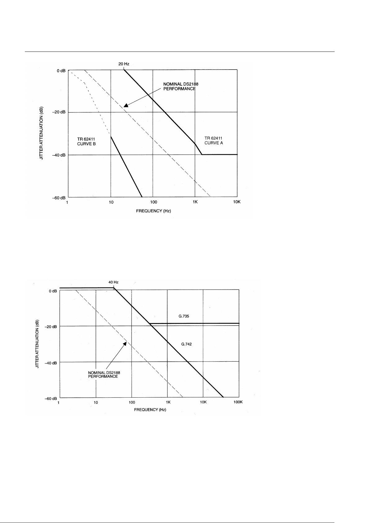
Limit) pin will remain low. Figures 1 and 2 illustrate the DS2188 Jitter Attenuator performance.
DS2188
T1/CEPT Jitter Attenuator
www.dalsemi.com
DJA 1 16 VDD
RPOS 2 15 RRPOS
RNEG 3 14 RRNEG
RCLK 4 13 RRCLK
BDS 5 12 RST
TEST 6 11 BL
XTAL OUT 7 10 XTAL2
VSS 8 9 XTAL1
16-Pin DIP/SOIC
Page 2

DS2188
2 of 11
If the incoming jitter has excursions greater than 120 UIpp, then the crystal is adjusted to track the shortterm frequency variations of the incoming signal so that there is no loss of data. This adjustment is
accomplished by dividing the 4X crystal by either 3 ½ or 4 ½ instead of 4. When the incoming jitter is
greater than 120 UIpp, the BL pin will transition high. When the incoming jitter returns to less than 120
UIpp, the BL pin will return low.
The jitter attenuator in the DS2188 can be disabled by tying the DJA pin high. When the jitter attenuator
is disabled, the FIFO is bypassed and jitter received at RCLK, RPOS and RNEG is passed through the
DS2188 to RRCLK, RRPOS, and RRNEG. In this situation, the BL pin has no significance and XTAL
OUT will not be coherent with RRCLK.
How to use the DS2188 with Dallas Semiconductor’s other T1 and CEPT line interface parts is illustrated
in Figures 3 through 5. Figure 3 illustrates how to use the DS2188 in the receive path along with a
DS2187 Receive Line Interface. Figure 4 illustrates how to use the DS2188 in the transmit path with the
DS2186 Transmit Line Interface. Also, see DS2188 Application Note, “Operation at Speeds Greater than
E1” for additional information.
BUFFER DEPTH SELECT
The buffer size on the DS2188 can be configured to either 128 or 32 bits via the BDS pin. If BDS is tied
low, then the buffer depth will be 128 bits and hence can handle input jitter up to 120 UIpp without losing
its full attenuation capabilities as is described above in the Over-view. If BDS is tied high, then the
buffer depth is shortened to 32 bits. In this configuration, the DS2188 can handle input jitter up to 28
UIpp without losing its full jitter attenuation capabilities. The user may wish to limit the buffer size to 32
bits in applications where through-put delay is critical or into existing applications that al-ready have 32
bits of buffer space.
RESET
The buffer on the DS2188 is automatically centered on power-up. The user can recenter the 128-bit (or
32-bit) buffer on demand via the RST pin. The RST pin on the DS2188 is negative-edge triggered. When
this pin transitions from high-to-low, the buffer is recentered. The RST pin can be held either high or low
during operation of the DS2188; only a negative going signal will initiate a recentering. In most cases, a
reset of the DS2188 will corrupt data that is currently passing through the buffer.
Page 3
DS2188
3 of 11
DS2188 TI JITTER ATTENUATION PERFORMANCE Figure 1
DS2188 CEPT JITTER ATTENUATION PERFORMANCE Figure 2
Page 4

DS2188
4 of 11
DS2188 IN THE RECEIVE PATH Figure 3
DS2188 IN THE TRANSMIT PATH Figure 4
Page 5

DS2188
5 of 11
PIN DESCRIPTION Table 1
PIN SYMBOL TYPE DESCRIPTION
1 DJA I
Disable Jitter Attenuation. When high, jittered data and clock at
RPOS, RNEG, and RCLK are passed directly to RRPOS,
RRNEG, and RRCLK.
2 RPOS I
Receive Positive Data Input. Jittered data input. Sampled on the
falling edge of RCLK.
3 RNEG I
Receive Negative Data Input. Jittered data input. Sampled on
the falling edge of RCLK.
4 RCLK I
Receive Clock Input. Jittered input 1.544 MHz or 2.048 MHz
clock.
5 BDS I
Buffer Depth Select.
0 = 128 bits
1 = 32 bits
6 TEST I
Test Input. In normal applications, this pin should be tied low.
When tied high, used to verify free running frequency of XTAL.
7 XTAL OUT O
Crystal Frequency Output. Buffered output of the 4X crystal connected
to XTAL1 and XTAL2.
8 V
SS
- Ground. 0.0 volts.
9
10
XTAL1
XTAL2
I
O
Crystal Connections. In T1 environments, connect a 6.176 MHz
crystal to these pins. In CEPT environments, connect a 8.192 MHz
crystal to these pins.
11 BL O
Buffer Limit. Transitions high when the buffer fills or empties to
within either 4 bits (BDS=0) or 2 bits (BDS=1) of its capacity. Indicates
that the jitter at RCLK is greater than 120 UIpp (BDS=0) or
28 UIpp (BDS=1).
12
RST
I
Reset. Negative-edge triggered; a high-low transition will recenter
the buffer. Activation of this pin may corrupt data through the
DS2188.
13 RRCLK O
Receive Reference Clock. Dejittered 1.544 MHz or 2.048 MHz
clock.
14 RRNEG O
Receive Reference Negative Data Output. Dejittered data output.
Updated on the rising edge of RRCLK.
15 RRPOS O
Receive Reference Positive Data Output. Dejittered data output.
Updated on the rising edge of RRCLK.
16 V
DD
- Positive Supply. 5.0 volts.
Page 6
DS2188
6 of 11
CRYSTAL REQUIREMENTS
The DS2188 must have a crystal connected to the XTAL1 and XTAL2 pins. For T1 environments, the
frequency of this crystal should be 6.176 MHz. For CEPT environments, the frequency of this crystal
should be 8.192 MHz. Table 2 lists some suggested crystal manufacturers that are recommended for use
with the DS2188. Also, see DS2188 Application Note, “Operation at Speeds Greater than E1” for
additional information.
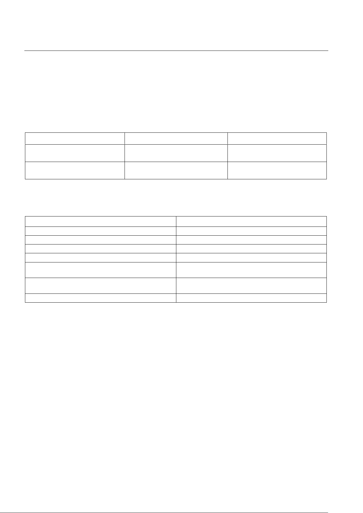
CRYSTAL MANUFACTURERS Table 2
MANUFACTURER PART #
FREQUENCY
JAN Crystal 6323-00, JC6A14
6323-00, JC8A14
6.176 MHz
8.192 MHz
M-TRON 4575-002
4575-001
6.176 MHz
8.192 MHz
CRYSTAL SELECTION GUIDELINES FOR THE DS2188
PARAMETER SPECIFICATION
Parallel resonant frequency 6.176 MHz (T1) or 8.192 MHz (CEPT)
Mode Fundamental
Load capacitance 14 to 20 pF (16 pF preferred)
Tolerance ±50 ppm over 0 to 70°C
Pullability
CL = 10 pF, delta_f = +175 to +250 ppm
CL = 45 pF, delta_f = -175 to -250 ppm
Effective series resistance
40 ohms maximum for 6.176 MHz
30 ohms maximum for 8.192 MHz
Crystal cut AT
Page 7
DS2188
7 of 11
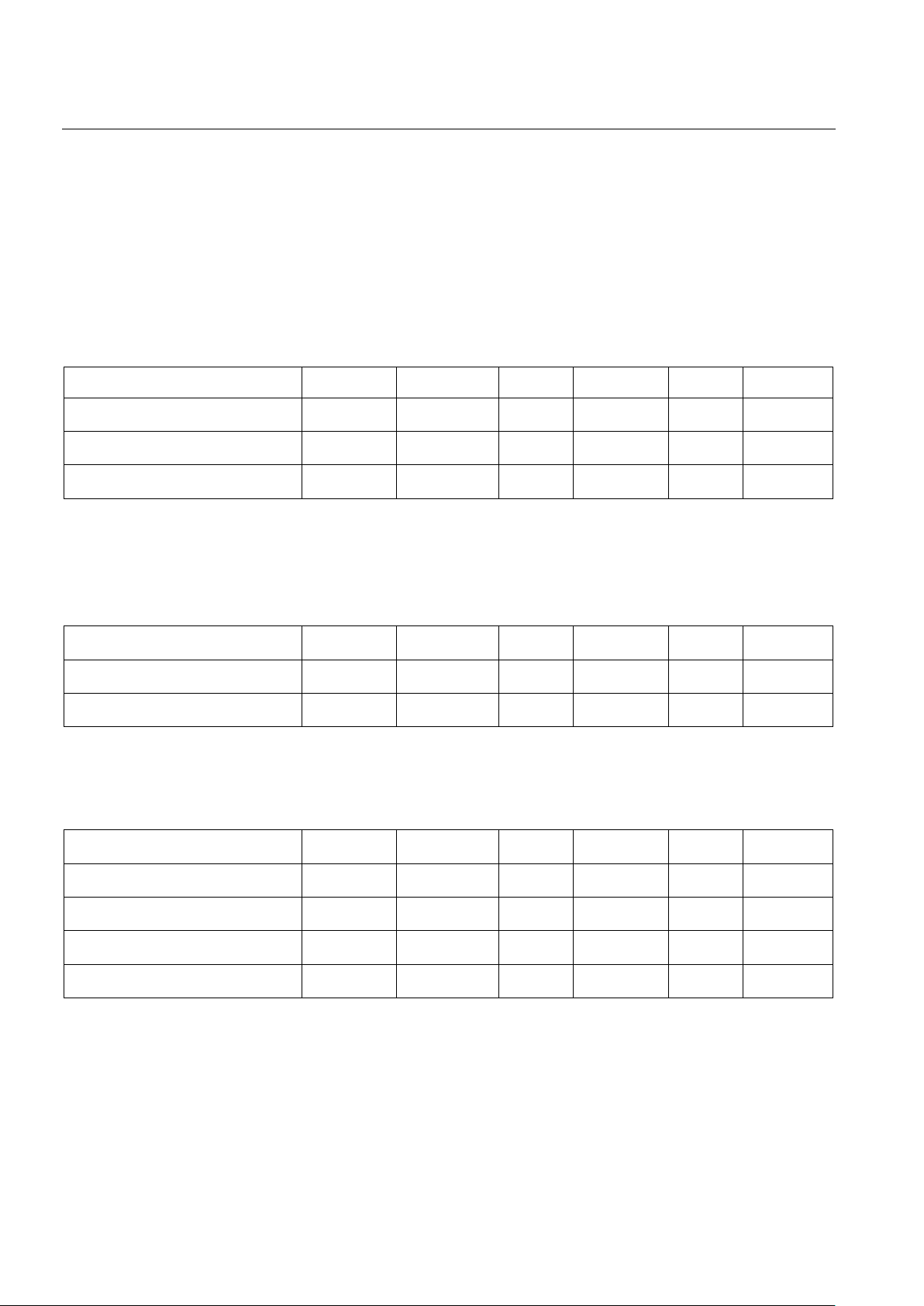
ABSOLUTE MAXIMUM RATINGS*
Voltage on Any Pin Relative to Ground -0.1V to +7.0V
Operating Temperature 0° to 70°C
Storage Temperature -55°C to +125°C
Soldering Temperature 260°C for 10 seconds
* This is a stress rating only and functional operation of the device at these or any other conditions above
those indicated in the operation sections of this specification is not implied. Exposure to absolute
maximum rating conditions for extended periods of time may affect reliability.
RECOMMENDED DC OPERATING CONDITIONS (0°C to 70°C)
PARAMETER SYMBOL MIN TYP MAX UNITS NOTES
Input Logic 1 V
IH
2.0 VCC+0.3 V 1
Input Logic 0 V
IL
-0.3 +0.8 V 1
Supply V
DD
4.50 5.50 V
NOTE:
1. Does not apply to XTAL1.
CAPACITANCE (tA=25°C)
PARAMETER SYMBOL MIN TYP MAX UNITS NOTES
Input Capacitance C
IN
5 pF
Output C
OUT
10 pF
DC ELECTRICAL CHARACTERISTICS (0°C to 70°C; VDD = 5.0V ± 10%)
PARAMETER SYMBOL MIN TYP MAX UNITS NOTES
Supply Current I
DD
7 12 mA 1
Input Leakage I
L
-1.0 +1.0 µA 2, 3
Output Current (2.4V) I
OH
-1.0 mA 3
Output Current (0.4V) I
OL
+4.0 mA 3
NOTES:
1. RCLK = 1.544 MHz; VDD = 5.50; outputs open.
2. VSS < VIN < VDD: XTAL1 = XTAL2 = VDD.
3. Does not apply to XTAL1 or XTAL2.
Page 8

DS2188
8 of 11
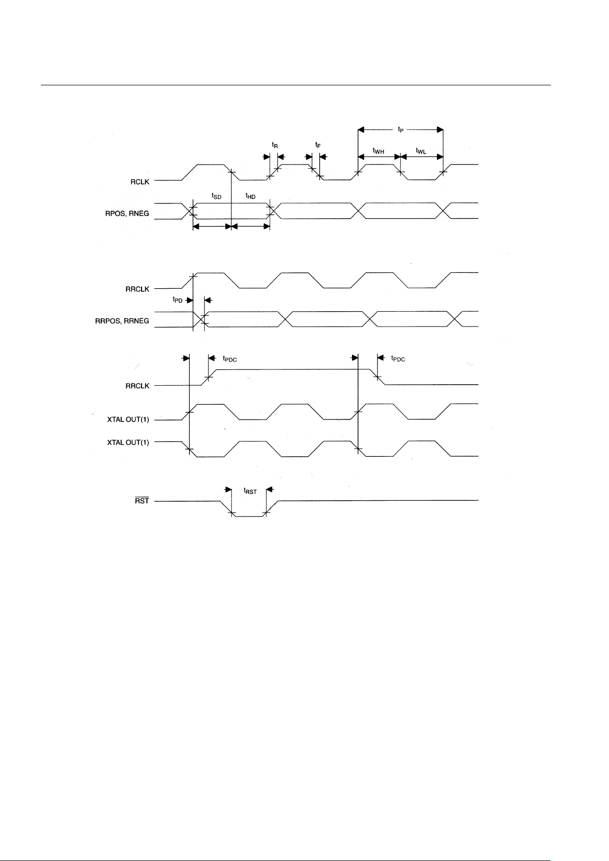
AC ELECTRICAL CHARACTERISTICS (0°C to 70°C; VDD = 5.0V ± 10%)
PARAMETER SYMBOL MIN TYP MAX UNITS NOTES
RCLK Period -200 +200 ppm 1
RCLK Pulse Width 100 ns
RCLK Rise and Fall Times 50 ns
RPOS, RNEG Setup to RCLK 50 ns
RPOS, RNEG Hold for
RCLK
50 ns
Propagation delay from
RRCLK to RPOS, RRNEG
Valid
50 ns
Propagation delay from
XTAL OUT to RRCLK
50 ns 2
RST Pulse Width
1 µA
NOTES:
1. The average period of RCLK must be within ±200 ppm of the fundamental frequency of the crystal
divided by four.
2. Only valid when the incoming jitter is less than 120 Ulpp (BDS=0) or 28 Ulpp (BDS=1).
Page 9
DS2188
9 of 11
AC TIMING DIAGRAM Figure 5
NOTE:
1. The phase relationship between XTAL OUT and RRCLK can be of either form.
Page 10
DS2188
10 of 11
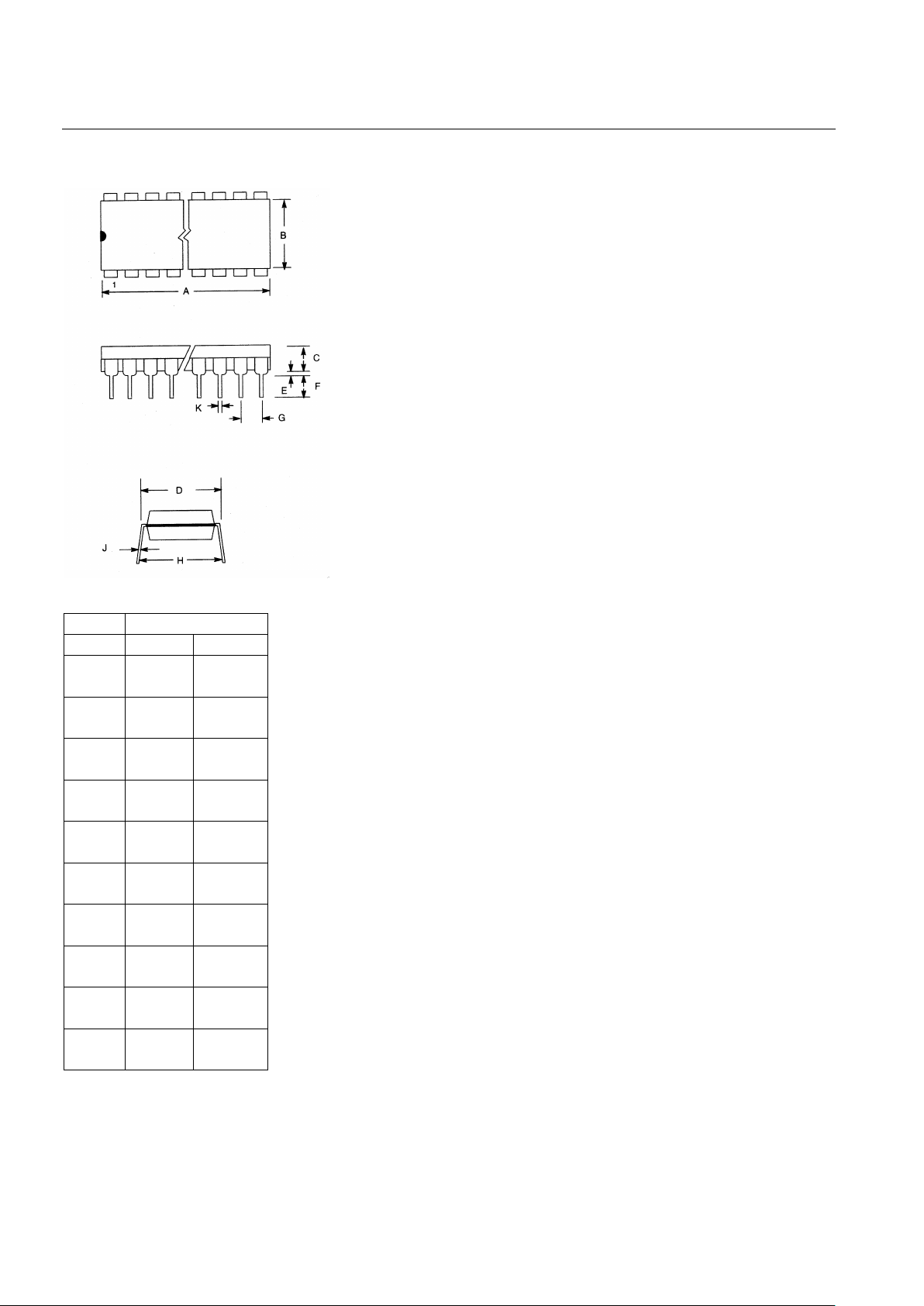
DS1288 T1/CEPT JITTER ATTENTUATOR 16-PIN DIP
PKG 16-PIN
DIM MIN MAX
AIN
MM
0.740
18.80
0.780
19.81
B IN
MM
0.240
6.10
0.260
6.60
C IN
MM
0.120
3.05
0.140
3.56
D IN
MM
0.300
7.62
0.325
8.26
E IN
MM
0.015
0.38
0.040
1.02
F IN
MM
0.120
3.04
0.140
1.02
G IN
MM
0.090
2.29
0.110
2.79
H IN
MM
0.320
8.13
0.370
9.40
J IN
MM
0.008
0.20
0.012
0.30
K IN
MM
0.015
0.38
0.021
0.53
Page 11
DS2188
11 of 11
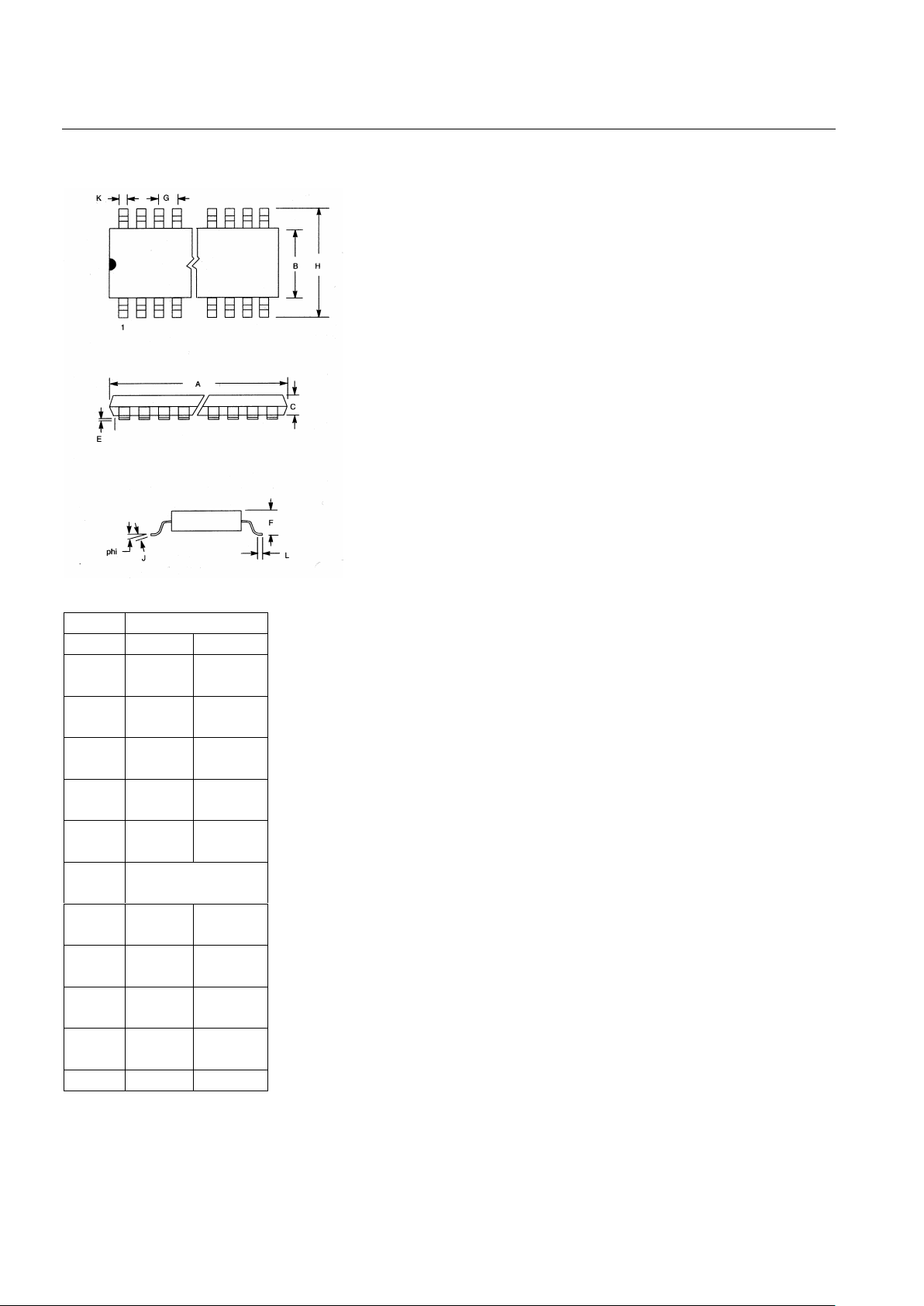
DS1288S T1/CEPT JITTER ATTENTUATOR 16-PIN SOIC
PKG 16-PIN
DIM MIN MAX
AIN
MM
0.402
10.21
0.412
10.46
B IN
MM
0.290
7.37
0.300
7.65
C IN
MM
0.089
2.26
0.095
2.41
E IN
MM
0.004
0.102
0.012
0.30
F IN
MM
0.094
2.38
0.105
2.68
G IN
MM
0.050 BSC
1.27 BSC
H IN
MM
0.398
10.11
0.416
10.57
J IN
MM
0.009
0.229
0.013
0.33
K IN
MM
0.013
0.33
0.019
0.48
L IN
MM
0.016
0.40
0.40
1.02
phi 0° 8°
 Loading...