

Page 1
查询DS2148供应商
www.maxim-ic.com
DS2148/DS21Q48
5V E1/T1/J1 Line Interface
FEATURES
§ Complete E1, T1, or J1 line interface unit
(LIU)
§ Supports both long- and short-haul trunks
§ Internal software-selectable receive-side
termination for 75Ω/100Ω/120W
§ 5V power supply
§ 32-bit or 128-bit crystal-less jitter attenuator
requires only a 2.048MHz master clock for
both E1 and T1 with option to use 1.544MHz
for T1
§ Generates the appropriate line build outs,
with and without return loss, for E1 and
DSX-1 and CSU line build outs for T1
§ AMI, HDB3, and B8ZS, encoding/decoding
§ 16.384MHz, 8.192MHz, 4.096MHz, or
2.048MHz clock output synthesized to
recovered clock
§ Programmable monitor mode for receiver
§ Loopbacks and PRBS pattern generation/
detection with output for received errors
§ Generates/detects in-band loop codes, 1 to 16
bits including CSU loop codes
§ 8-bit parallel or serial interface with optional
hardware mode
§ Multiplexed and nonmultiplexed parallel bus
supports Intel or Motorola
§ Detects/generates blue (AIS) alarms
§ NRZ/bipolar interface for TX/RX data I/O
§ Transmit open-circuit detection
§ Receive Carrier Loss (RCL) indication
(G.775)
§ High-Z State for TTIP and TRING
§ 50mA (rms) current limiter
PIN DESCRIPTION
44
1
44 TQFP
7mm
CABGA
ORDERING INFORMATION
Single-Channel Devices:
DS2148TN 44-Pin TQFP (-40°C to +85°C)
DS2148T 44-Pin TQFP (0o C to +70o C)
DS2148GN 7mm CABGA (-40°C to +85°C)
DS2148G 7mm CABGA (0
Four-Channel Devices:
DS21Q48N (Quad) BGA (-40°C to +85°C)
DS21Q48 (Quad) BGA (0o C to +70oC)
o
C to +70o C)
1 of 75 REV: 082504
Page 2

DS2148/Q48
DESCRIPTION
The DS2148 is a complete selectable E1 or T1 Line Interface Unit (LIU) for short- and long-haul
applications. Throughout the data sheet, J1 is represented wherever T1 exists. Receive sensitivity adjusts
automatically to the incoming signal and can be programmed for 0dB to 12dB or 0dB to 43dB for E1
applications and 0dB to 30dB or 0dB to 36dB for T1 applications. The device can generate the necessary
G.703 E1 waveshapes in 75Ω or 120Ω applications and DSX-1 line build outs or CSU line build outs of
0dB, -7.5dB, -15dB, and -22.5dB for T1 applications. The crystal-less onboard jitter attenuator requires
only a 2.048MHz MCLK for both E1 and T1 applications (with the option of using a 1.544MHz MCLK
in T1 applications). The jitter attenuator FIFO is selectable to either 32 bits or 128 bits in depth and can
be placed in either the transmit or receive data paths. An X 2.048MHz output clock synthesized to RCLK
is available for use as a backplane system clock (where n = 1, 2, 4, or 8). The DS2148 has diagnostic
capabilities such as loopbacks and PRBS pattern generation/detection. 16-bit loop-up and loop-down
codes can be generated and detected. The device can be controlled via an 8-bit parallel muxed or
nonmuxed port, serial port or used in hardware mode. The device fully meets all of the latest E1 and T1
specifications including ANSI T1.403-1999, ANSI T1.408, AT&T TR 62411, ITU G.703, G.704, G.706,
G.736, G.775, G.823, I.431, O.151, O.161, ETSI ETS 300 166, JTG.703, JTI.431, JJ-20.1, TBR12,
TBR13, and CTR4.
2 of 75
Page 3

DS2148/Q48
TABLE OF CONTENTS
1. LIST OF FIGURES............................................................................................................................... 4
2. LIST OF TABLES ................................................................................................................................ 5
3. INTRODUCTION................................................................................................................................. 6
3.1 DOCUMENT REVISION HISTORY ............................................................................................6
4. PIN DESCRIPTION ............................................................................................................................. 9
5. HARDWARE MODE ......................................................................................................................... 22
5.1 REGISTER MAP .......................................................................................................................... 23
5.2 PARALLEL PORT OPERATION................................................................................................ 24
5.3 SERIAL PORT OPERATION ...................................................................................................... 24
6. CONTROL REGISTERS.................................................................................................................... 28
6.1 DEVICE POWER-UP AND RESET ............................................................................................ 31
7 STATUS REGISTERS ....................................................................................................................... 34
8. DIAGNOSTICS .................................................................................................................................. 39
8.1 IN-BAND LOOP CODE GENERATION AND DETECTION ...................................................39
8.2 LOOPBACKS ............................................................................................................................... 43
8.2.1 Remote Loopback (RLB)......................................................................................................... 43
8.2.2 Local Loopback (LLB)............................................................................................................ 43
8.2.3 Analog Loopback (LLB) ......................................................................................................... 44
8.2.4 Dual Loopback (DLB) ............................................................................................................ 44
8.3 PRBS GENERATION AND DETECTION ................................................................................. 44
8.4 ERROR COUNTER...................................................................................................................... 44
8.4.1 Error Counter Update ............................................................................................................45
8.5 ERROR INSERTION.................................................................................................................... 45
9. ANALOG INTERFACE .....................................................................................................................46
9.1 RECEIVER .................................................................................................................................... 46
9.2 TRANSMITTER ........................................................................................................................... 47
9.3 JITTER ATTENUATOR ..............................................................................................................47
9.4 G.703 SYNCHRONIZATION SIGNAL ......................................................................................48
10. DS21Q48 QUAD LIU......................................................................................................................... 56
11. DC CHARACTERISTICS.................................................................................................................. 60
12. AC CHARACTERISTICS.................................................................................................................. 62
13. MECHANICAL DIMENSIONS......................................................................................................... 71
13.1 MECHANICAL DIMENSIONS—QUAD VERSION................................................................. 73
3 of 75
Page 4

DS2148/Q48
1. LIST OF FIGURES
Figure 3-1 DS2148 BLOCK DIAGRAM..................................................................................................... 7
Figure 3-2 RECEIVE LOGIC ...................................................................................................................... 8
Figure 3-3 TRANSMIT LOGIC................................................................................................................... 9
Figure 4-1 PARALLEL PORT MODE PINOUT (BIS1 = 0, BIS0 = 1 or 0) ............................................ 21
Figure 4-2 SERIAL PORT MODE PINOUT (BIS1 = 1, BIS0 = 0) .......................................................... 21
Figure 4-3 HARDWARE MODE PINOUT (BIS1 = 1, BIS0 = 1) ............................................................ 22
Figure 5-1 SERIAL PORT OPERATION FOR READ ACCESS (R=1) MODE 1.................................. 25
Figure 5-2 SERIAL PORT OPERATION FOR READ ACCESS MODE 2 ............................................. 25
Figure 5-3 SERIAL PORT OPERATION FOR READ ACCESS MODE 3 ............................................. 26
Figure 5-4 SERIAL PORT OPERATION FOR READ ACCESS MODE 4 ............................................. 26
Figure 5-5 SERIAL PORT OPERATION FOR WRITE ACCESS (R=0) MODES 1&2 ...……………27
Figure 5-6 SERIAL PORT OPERATION FOR WRITE ACCESS MODES 3&4 …………...…………27
Figure 9-1 BASIC INTERFACE ………………………………………………………………………..50
Figure 9-2 PROTECTED INTERFACE USING INTERNAL RECEIVE TERMINATION.................... 51
Figure 9-3 PROTECTED INTERFACE USING EXTERNAL RECEIVE TERMINATION .................. 52
Figure 9-4 E1 TRANSMIT PULSE TEMPLATE...................................................................................... 53
Figure 9-5 T1 TRANSMIT PULSE TEMPLATE...................................................................................... 54
Figure 9-6 JITTER TOLERANCE............................................................................................................. 55
Figure 9-7 JITTER ATTENUATION ........................................................................................................ 55
Figure 10-1 BGA 12 x 12 PIN LAYOUT .................................................................................................. 59
Figure 12-1 INTEL BUS READ TIMING (PBTS = 0, BIS1 = 0, BIS0 = 0) ............................................ 63
Figure 12-2 INTEL BUS WRITE TIMING (PBTS = 0, BIS1 = 0, BIS0 = 0)........................................... 63
Figure 12-3 MOTOROLA BUS TIMING (PBTS = 1, BIS1 = 0, BIS0 = 0) ............................................ 64
Figure 12-4 INTEL BUS READ TIMING (PBTS = 0, BIS1 = 0, BIS0 = 1) ............................................ 66
Figure 12-5 INTEL BUS WRITE TIMING (PBTS = 0, BIS1 = 0, BIS0 = 1)........................................... 66
Figure 12-6 MOTOROLA BUS READ TIMING (PBTS = 1, BIS1 = 0, BIS0 = 1) ................................. 67
Figure 12-7 MOTOROLA BUS WRITE TIMING (PBTS = 1, BIS1 = 0, BIS0 = 1)................................ 67
Figure 12-8 SERIAL BUS TIMING (BIS1 = 1, BIS0 = 0)........................................................................ 68
Figure 12-9 RECEIVE SIDE TIMING ...................................................................................................... 69
Figure 12-10 TRANSMIT SIDE TIMING................................................................................................. 70
4 of 75
Page 5

DS2148/Q48
2. LIST OF TABLES
Table 4-1 BUS INTERFACE SELECTION ................................................................................................ 9
Table 4-2a PIN ASSIGNMENT ................................................................................................................. 10
Table 4-2b PIN DESCRIPTIONS (Sorted by Pin Name, DS2148T Pin Numbering) ............................... 11
Table 4-3a PIN ASSIGNMENT IN SERIAL PORT MODE..................................................................... 13
Table 4-3b PIN DESCRIPTIONS IN SERIAL PORT MODE (Sorted by Pin Name, DS2148T Pin
Numbering) .......................................................................................................................................... 14
Table 4-4a PIN ASSIGNMENT IN HARDWARE MODE....................................................................... 16
Table 4-4b PIN DESCRIPTIONS IN HARDWARE MODE (Sorted by Pin Name, DS2148T Pin
Numbering) .......................................................................................................................................... 16
Table 4-5 LOOPBACK CONTROL IN HARDWARE MODE ................................................................ 20
Table 4-6 TRANSMIT DATA CONTROL IN HARDWARE MODE ..................................................... 20
Table 4-7 RECEIVE SENSITIVITY SETTINGS...................................................................................... 20
Table 4-8 MONITOR GAIN SETTINGS .................................................................................................. 20
Table 4-9 INTERNAL RX TERMINATION SELECT............................................................................. 20
Table 4-10 MCLK SELECTION................................................................................................................ 20
Table 5-1 REGISTER MAP ....................................................................................................................... 23
Table 6-1 MCLK SELECTION.................................................................................................................. 29
Table 6-2 RECEIVE SENSITIVITY SETTINGS...................................................................................... 31
Table 6-3 BACK PLANE CLOCK SELECT............................................................................................. 32
Table 6-4 MONITOR GAIN SETTINGS .................................................................................................. 32
Table 6-5 INTERNAL RX TERMINATION SELECT............................................................................. 33
Table 7-1 RECEIVED ALARM CRITERIA ............................................................................................. 35
Table 7-2 RECEIVE LEVEL INDICATION............................................................................................. 38
Table 8-1 TRANSMIT CODE LENGTH................................................................................................... 40
Table 8-2 RECEIVE CODE LENGTH ...................................................................................................... 40
Table 8-3 DEFINITION OF RECEIVED ERRORS.................................................................................. 44
Table 8-4 FUNCTION OF ECRS BITS AND RNEG PIN........................................................................ 45
Table 9-1 LINE BUILD OUT SELECT FOR E1 IN REGISTER CCR4 (ETS = 0) ................................. 48
Table 9-2 LINE BUILD OUT SELECT FOR T1 IN REGISTER CCR4 (ETS = 1) ................................. 48
Table 9-3 TRANSFORMER SPECIFICATIONS FOR 5V OPERATION ............................................... 49
Table 10-1 DS21Q48 PIN ASSIGNMENT................................................................................................ 56
5 of 75
Page 6

DS2148/Q48
3. INTRODUCTION
The analog AMI/HDB3 waveform off the E1 line or the AMI/B8ZS waveform off the T1 line is
transformer coupled into the RTIP and RRING pins of the DS2148. The user has the option to use
internal software-selectable receive-side termination for 75Ω/100Ω/120W applications or external
termination. The device recovers clock and data from the analog signal and passes it through the jitter
attenuation MUX outputting the received line clock at RCLK and bipolar or NRZ data at RPOS and
RNEG. The DS2148 contains an active filter that reconstructs the analog-received signal for the nonlinear
losses that occur in transmission. The receive circuitry also is configurable for various monitor
applications. The device has a usable receive sensitivity of 0dB to -43dB (E1) and 0dB to -36dB (T1),
which allows the device to operate on 0.63mm (22AWG) cables up to 2.5km (E1) and 6k feet (T1) in
length. Data input at TPOS and TNEG is sent via the jitter attenuation MUX to the waveshaping circuitry
and line driver. The DS2148 will drive the E1 or T1 line from the TTIP and TRING pins via a coupling
transformer. The line driver can handle both CEPT 30/ISDN-PRI lines for E1 and long-haul (CSU) or
short-haul (DSX-1) lines for T1.
3.1 DOCUMENT REVISION HISTORY
1) 100W/60W termination reversed in Internal Rx Termination Select tables, 091799.
2) Add DS21Q48 pinout, 092899.
3) Correct VSM pin number in Q48 (12 x 12 BGA) from G5 to G4, 120699.
4) Add timing diagram for Status Register (write access mode); Add mechanical dimensions for the
quad version, 032900.
5) Timing diagram for Status Register (write access mode) added; elaboration on burst mode bit; add
mechanical dimensions for the quad version, 050300.
6) Changes to datasheet to indicate 5V only part, 011801.
7) Added supply current measurement; added thermal characteristics of quad package, 092001.
8) Corrected typos and removed instances of 3V operation, 082504.
6 of 75
Page 7
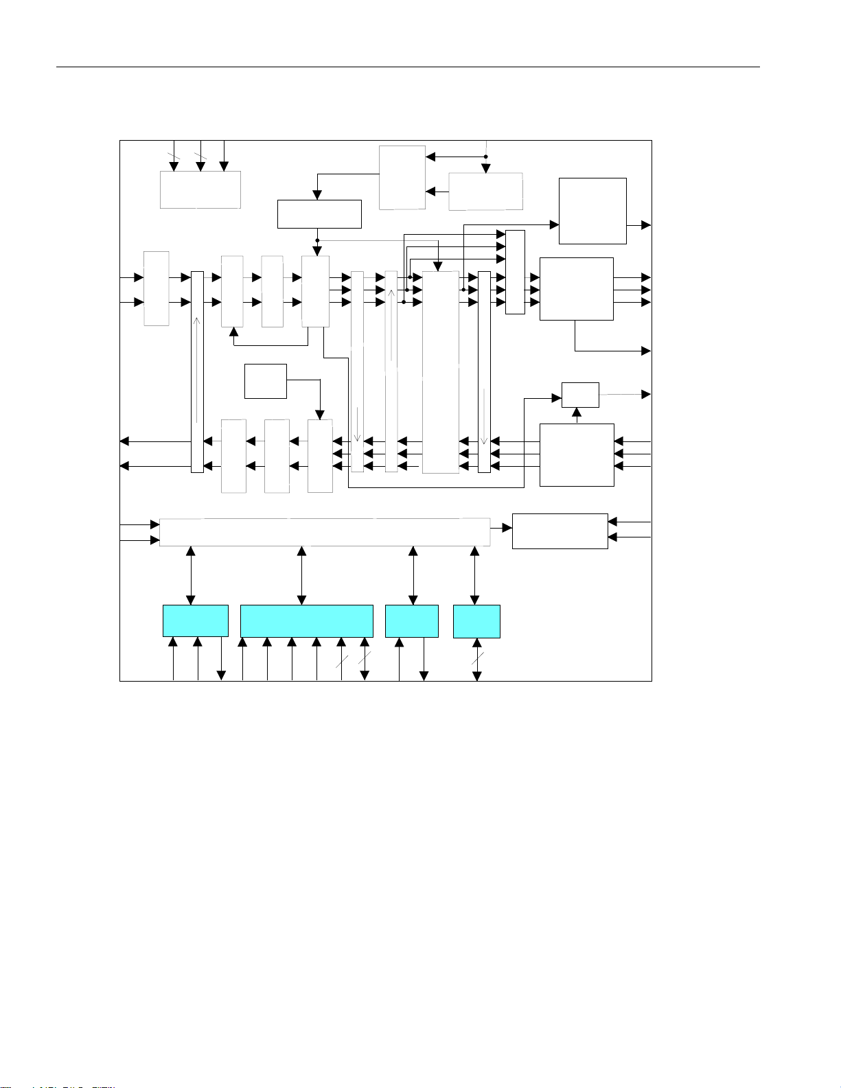
DS2148 BLOCK DIAGRAM Figure 3-1
S
D
S
D
V
2
w
e
o
P
R
N
R
G
I
R
T
P
I
T
N
R
G
I
T
T
P
I
Optional
Termination
VSM
V
2
s
n
o
i
t
c
e
n
n
C
o
r
t
c
e
t
r
e
e
t
D
l
i
k
F
a
e
P
k
c
a
b
p
o
o
L
g
o
l
a
n
A
Unframed
All Ones
Insertion
s
r
e
v
i
r
D
e
n
i
L
s
r
e
t
l
i
F
U
S
C
JACLK
L
L
P
C
/
O
V
a
t
y
a
r
e
D
v
/
o
k
c
c
e
o
l
R
C
g
n
i
p
a
h
S
e
v
a
W
Remote Loopback (Dual Mode)
Jitter
Attenuator
MUX
DS2148/Q48
K
L
C
M
2.048MHz to
1.544MHz PLL
)
h
t
a
p
e
v
i
e
c
e
r
r
o
t
n
i
o
i
t
m
s
a
n
u
a
n
r
t
e
t
t
r
e
A
h
r
k
c
a
b
p
o
o
L
l
a
c
o
L
t
i
e
t
e
t
i
n
J
i
d
e
c
a
l
p
e
b
n
a
c
(
MUX
k
c
a
b
p
o
o
L
e
t
o
m
e
R
16.384MHz or
8.1 92MHz or
4.0 96MHz or
2.048MHz
Synthesizer
See Figure 3-2
MUX RCL/LOTC
See Figure 3-3
BPCLK
RPOS
RCLK
RNEG
PBEO
TPOS
TCLK
TNEG
S
I
B
1
S
I
B
0
U
X
M
r
e
t
r
e
n
I
i
S
l
a
I
K
D
L
S
C
S
l
a
r
e
i
S
e
h
t
(
e
c
a
f
O
S
D
T
S
B
P
n
a
,
l
e
l
l
a
P
,
r
a
r
a
a
P
)
*
W
/
R
(
*
R
W
e
r
H
a
r
w
a
d
d
c
e
l
l
e
r
e
t
a
n
f
I
l
)
)
*
S
S
A
D
(
(
E
*
L
D
A
R
s
r
e
c
t
n
I
5
4
A
o
t
0
A
r
a
f
a
h
s
e
e
C
o
n
I
8
7
/
D
7
A
D
o
o
t
t
0
0
D
D
A
)
i
s
n
v
c
e
d
p
i
e
r
H
a
r
w
a
d
r
t
n
l
o
d
n
a
r
e
t
r
t
p
u
*
*
T
S
N
C
I
e
r
e
c
t
a
n
f
I
e
1
2
r
t
n
l
C
o
o
a
t
d
e
t
u
o
(
r
r
s
o
t
P
t
T
d
e
n
s
c
o
)
k
l
b
l
l
a
o
HRST*
TEST
7 of 75
Page 8
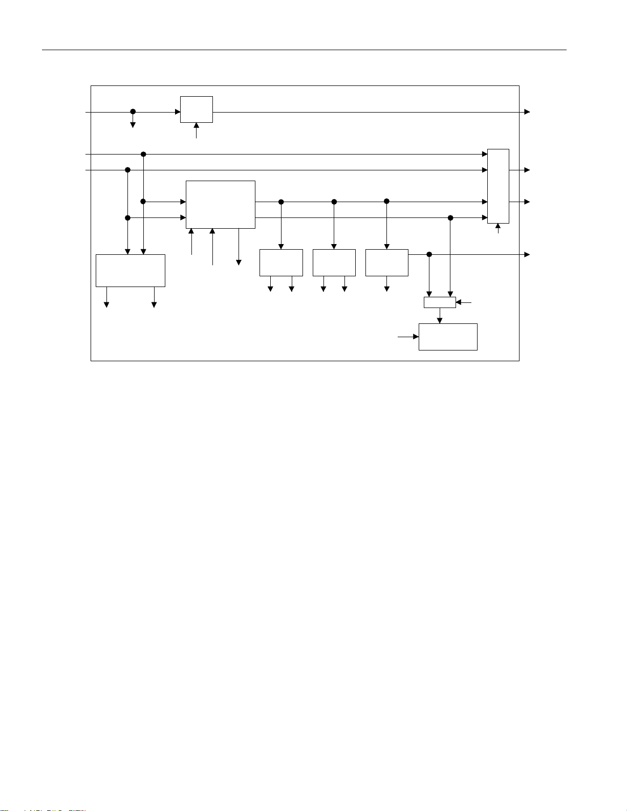
RECEIVE LOGIC Figure 3-2
DS2148/Q48
From
Remote
Loopback
Routed to
All Blocks
4 or 8 Zero Detect
16 Zero Detect
RIR1.7 RIR1.6
Clock
Invert
CCR2.0
CCR2.3
CCR6.2/
CCR6.0/
CCR6.1
B8ZS/HDB3
Decoder
RIR1.5
All Ones
Detector
NRZ Data
BPV/CV/EXZ
Loop Code
Detector
SR.6 SR.7SR.4 RIR1.3
PRBS
Detector
SR.0
CCR1.4
mux
16-Bit Error
Counter (ECR)
RCLK
RPOS
mux
RNEG
CCR1.6
PBEO
CCR6.0
rx bd
8 of 75
Page 9
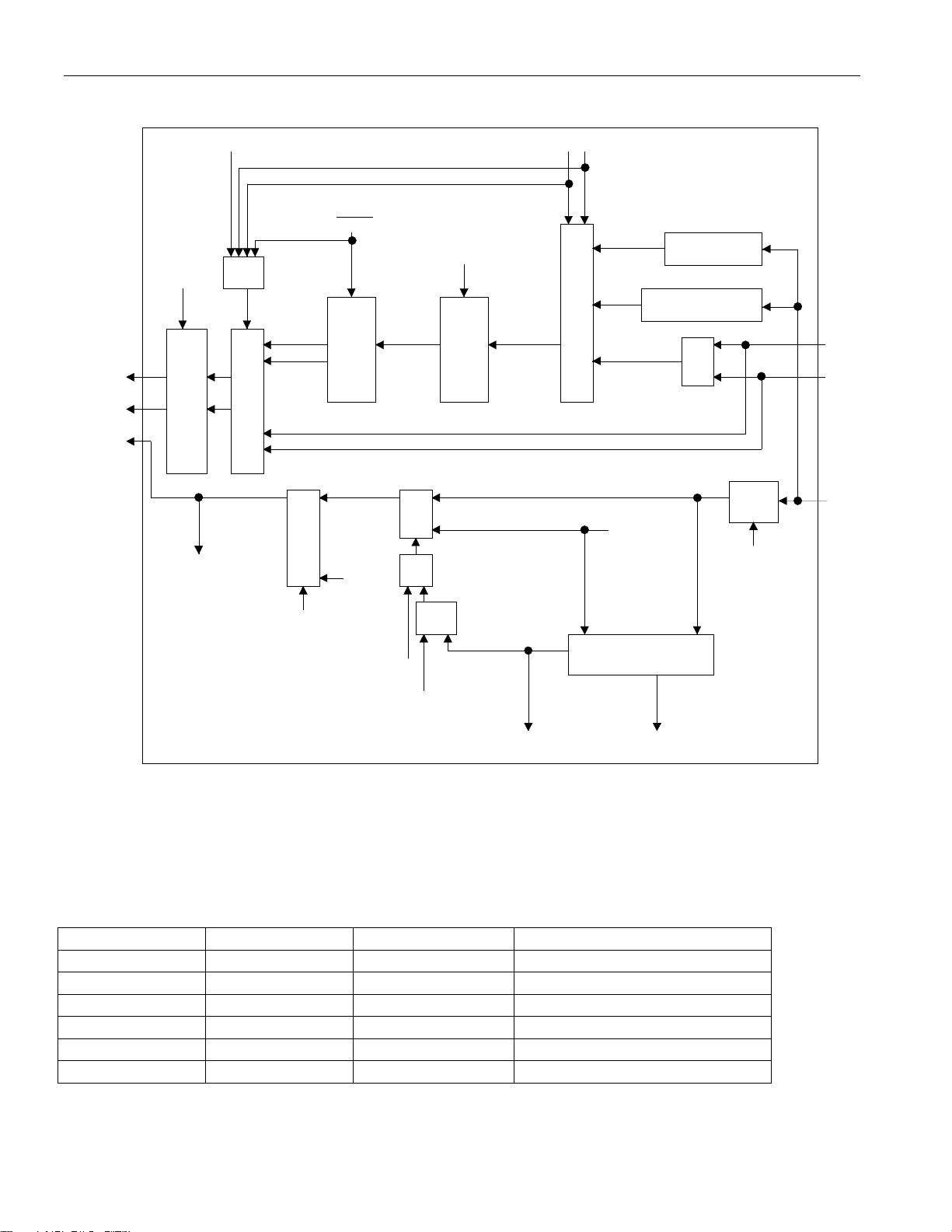
TRANSMIT LOGIC Figure 3-3
CCR1.6
CCR2.2
OR
Gate
mux
1
0
mux
B8ZS/
HDB3
Coder
0
1
RCLK
To
Remote
Loopback
CCR3.1
BPV
Insert
Routed to
All Blocks
mux
OR
Gate
CCR3.0
Logic
Error
Insert
0
1
CCR3.3
mux
CCR3.4
PRBS Generator
Loop Code Generator
JACLK
(derived
from
MCLK)
OR
Gate
Clock
Invert
CCR2.1
DS2148/Q48
TPOS
TNEG
TCLK
CCR1.1
CCR1.2
AND
Gate
CCR1.0
To LOTC Output Pin
Loss Of Transmit
Clock Detect
tx bd
SR.5
4. PIN DESCRIPTION
The DS2148 can be controlled in a parallel port mode, a serial port mode, or a hardware mode (Table 4-1,
4-2, and 4-3). The parallel and serial port modes are described in Section 3, and the hardware mode is
described below.
BUS INTERFACE SELECTION Table 4-1
BIS1 BIS0 PBTS BUS INTERFACE TYPE
0 0 0 Muxed Intel
0 0 1 Muxed Motorola
0 1 0 Nonmuxed Intel
0 1 1 Nonmuxed Motorola
1 0 - Serial Port
1 1 - Hardware
9 of 75
Page 10
PIN ASSIGNMENT IN PARALLEL PORT MODE Table 4-2a
DS2148T
PIN #
1
2 C2 I RD*(DS*)
3 B1 I WR*(R/W*)
4 D2 I ALE(AS)
5 C1 I NA
6 D3 I NA
7 D1 I/O A4
8 E1 I A3
9 F2 I A2
10 F1 I A1
11 G1 I A0
12 E3 I/O D7/AD7
13 F3 I/O D6/AD6
14 G2 I/O D5/AD5
15 F4 I/O D4/AD4
16 G3 I/O D3/AD3
17 E4 I/O D2/AD2
18 G4 I/O D1/AD1
19 F5 I/O D0/AD0
20 G5 I VSM
21 F6 - VDD
22 G6 - VSS
23 E5 I/O INT*
24 E6 O PBEO
25 F7 O RCL/LOTC
26 D6 I TEST
27 D5 I RTIP
28 D7 I RRING
29 C6 I HRST*
30 C7 I MCLK
31 B6 O BPCLK
32 B7 I BIS0
33 A7 I BIS1
34 C5 O TTIP
35 B5 - VSS
36 A6 - VDD
37 B4 O TRING
38 C4 O RPOS
39 A4 O RNEG
40 B3 O RCLK
41 A3 I TPOS
42 B2 I TNEG
43 A2 I TCLK
44 A1 I PBTS
DS2148G
PIN#
I/O Parallel
Port Mode
C3 I CS*
DS2148/Q48
10 of 75
Page 11

DS2148/Q48
PIN DESCRIPTIONS IN PARALLEL PORT MODE (Sorted by Pin Name,
DS2148T Pin Numbering) Table 4-2b
ACRONYM PIN I/O DESCRIPTION
A0
To
A4
ALE
(AS)
BIS0/
BIS1
BPCLK 31 O Back Plane Clock. A 16.384MHz, 8.192MHz, 4.096MHz, or
CS* 1 I Chip Select. Must be low to read or write to the device. CS* is an
D0 / AD0
To
D7 / AD7
HRST* 29 I Hardware Reset. Bringing HRST* low will reset the DS2148
INT* 23 O Interrupt [INT*] pin 23. Flags host controller during conditions
MCLK 30 I Master Clock. A 2.048MHz (±50ppm) clock source with TTL
NA
PBEO 24 O PRBS Bit Error Output. The receiver will constantly search for a
PBTS 44 I Parallel Bus Type Select. When using the parallel port (BIS1 = 0),
11
to
7
4 I Address Latch Enable (Address Strobe). When using the parallel
32/
33
19
to
12
- I Not Assigned. Should be tied low.
I Address Bus. In nonmultiplexed bus operation (BIS1 = 0, BIS0 =
1), serves as the address bus. In multiplexed bus operation (BIS1 =
0, BIS0 = 0), these pins are not used and should be tied low.
port (BIS1 = 0) in multiplexed bus mode (BIS0 = 0), serves to
demultiplex the bus on a positive-going edge. In nonmultiplexed bus
mode (BIS0 = 1), should be tied low.
I Bus Interface Select Bits 0 & 1. Used to select bus interface option.
See Table 4-1 for details.
2.048MHz clock output that is referenced to RCLK selectable via
CCR5.7 and CCR5.6. In hardware mode, defaults to 16.384MHz
output.
active low signal.
I/O Data Bus/Address/Data Bus. In non-multiplexed bus operation
(BIS1 = 0, BIS0 = 1), serves as the data bus. In multiplexed bus
operation (BIS1 = 0, BIS0 = 0), serves as an 8-bit multiplexed
address/data bus.
setting all control bits to their default state of all zeros.
and change of conditions defined in the Status Register. Active low,
open drain output.
levels is applied at this pin. This clock is used internally for both
clock/data recovery and for jitter attenuation. Use of a T1 1.544MHz
clock source is optional.
See Note 1 on clock accuracy at the end of this table.
215-1 or a 220-1 PRBS depending on the ETS bit setting (CCR1.7).
Remains high if out of synchronization with the PRBS pattern. Goes
low when synchronized to the PRBS pattern. Any errors in the
received pattern after synchronization will cause a positive going
pulse (with same period as E1 or T1 clock) synchronous with
RCLK. PRBS bit errors can also be reported to the ECR1 and ECR2
registers by setting CCR6.2 to a logic 1.
set high to select Motorola bus timing, set low to select Intel bus
timing. This pin controls the function of the RD*(DS*), ALE(AS),
and WR*(R/W*) pins. If PBTS = 1 and BIS1 = 0, then these pins
assume the Motorola function listed in parenthesis (). In serial port
mode, this pin should be tied low.
11 of 75
Page 12

DS2148/Q48
ACRONYM PIN I/O DESCRIPTION
RCLK
40 O Receive Clock. Buffered recovered clock from the line.
Synchronous to MCLK in absence of signal at RTIP and RRING.
RD*
(DS*)
2 I Read Input (Data Strobe). RD* and DS* are active low signals.
DS active low when in nonmultiplexed, Motorola mode. See the Bus
Timing Diagrams in Section 12.
RCL/
LOTC
25 O Receive Carrier Loss/Loss of Transmit Clock. An output which
will toggle high during a receive carrier loss (CCR2.7 = 0) or will
toggle high if the TCLK pin has not been toggled for 5msec ± 2msec
(CCR2.7 = 1). CCR2.7 defaults to logic 0 when in hardware mode.
RNEG
39 O Receive Negative Data. Updated on the rising edge (CCR2.0 = 0)
or the falling edge (CCR2.0 = 1) of RCLK with the bipolar data out
of the line interface. Set NRZE (CCR1.6) to a one for NRZ
applications. In NRZ mode, data will be output on RPOS while a
received error will cause a positive-going pulse synchronous with
RCLK at RNEG. See Section 8.4 for details.
RPOS 38 O Receive Positive Data. Updated on the rising edge (CCR2.0 = 0) or
the falling edge (CCR2.0 = 1) of RCLK with bipolar data out of the
line interface. Set NRZE (CCR1.6) to a one for NRZ applications. In
NRZ mode, data will be output on RPOS while a received error will
cause a positive-going pulse synchronous with RCLK at RNEG. See
Section 8.4 for details.
RTIP/
RRING
27/
28
I Receive Tip and Ring. Analog inputs for clock recovery circuitry.
These pins connect via a 1:1 transformer to the line. See Section 7
for details.
TCLK 43 I Transmit Clock. A 2.048MHz or 1.544MHz primary clock. Used to
clock data through the transmit side formatter. Can be sourced
internally by MCLK or RCLK. See Common Control Register 1 and
Figure 3-3.
TEST 26 I 3-state Control. Set high to 3-state all outputs and I/O pins
(including the parallel control port). Set low for normal operation.
Useful in board level testing.
TNEG 42 I Transmit Negative Data. Sampled on the falling edge (CCR2.1 =
0) or the rising edge (CCR2.1 = 1) of TCLK for data to be
transmitted out onto the line.
TPOS 41 I Transmit Positive Data. Sampled on the falling edge (CCR2.1 = 0)
or the rising edge (CCR2.1 = 1) of TCLK for data to be transmitted
out onto the line.
TTIP/
TRING
34/
37
O Transmit Tip and Ring [TTIP & TRING]. Analog line driver
outputs. These pins connect via a step-up transformer to the line. See
Section 7 for details.
VDD
21/
- Positive Supply. 5.0V ±5%
36
VSM 20 I Voltage Supply Mode. Should be tied high for 5V operation
VSS 22/
35
WR*
3 I Write Input (Read/Write). WR* is an active low signal. See the
(R/W*)
-
Signal Ground.
Bus Timing Diagrams in Section 12.
12 of 75
Page 13
PIN ASSIGNMENT IN SERIAL PORT MODE Table 4-3a
DS2148T
PIN #
1
2 C2 I NA
3 B1 I NA
4 D2 I NA
5 C1 I SCLK
6 D3 I SDI
7 D1 I/O SDO
8 E1 I ICES
9 F2 I OCES
10 F1 I NA
11 G1 I NA
12 E3 I/O NA
13 F3 I/O NA
14 G2 I/O NA
15 F4 I/O NA
16 G3 I/O NA
17 E4 I/O NA
18 G4 I/O NA
19 F5 I/O NA
20 G5 I VSM
21 F6 - VDD
22 G6 - VSS
23 E5 I/O INT*
24 E6 O PBEO
25 F7 O RCL/LOTC
26 D6 I TEST
27 D5 I RTIP
28 D7 I RRING
29 C6 I HRST*
30 C7 I MCLK
31 B6 O BPCLK
32 B7 I BIS0
33 A7 I BIS1
34 C5 O TTIP
35 B5 - VSS
36 A6 - VDD
37 B4 O TRING
38 C4 O RPOS
39 A4 O RNEG
40 B3 O RCLK
41 A3 I TPOS
42 B2 I TNEG
43 A2 I TCLK
44 A1 I NA
DS2148G
PIN#
I/O Serial
Port Mode
C3 I CS*
DS2148/Q48
13 of 75
Page 14

DS2148/Q48
PIN DESCRIPTIONS IN SERIAL PORT MODE (Sorted by Pin Name, DS2148T
Pin Numbering) Table 4-3b
ACRONYM PIN I/O DESCRIPTION
BIS0/
BIS1
BPCLK 31 O Back Plane Clock. A 16.384MHz, 8.192MHz, 4.096MHz, or
CS* 1 I Chip Select. Must be low to read or write to the device. CS* is an
HRST* 29 I Hardware Reset. Bringing HRST* low will reset the DS2148
ICES
INT* 23 O Interrupt [INT*] pin 23. Flags host controller during conditions
MCLK 30 I Master Clock. A 2.048MHz (±50ppm) clock source with TTL
NA
OCES 9 I Output Clock Edge Select. Selects whether the serial port data
PBEO 24 O PRBS Bit Error Output. The receiver will constantly search for a
RCLK
RCL/
LOTC
32/
33
8 I Input Clock Edge Select. Selects whether the serial port data input
- I Not Assigned. Should be tied low.
40 O Receive Clock. Buffered recovered clock from the line.
25 O Receive Carrier Loss / Loss of Transmit Clock. An output which
I Bus Interface Select Bits 0 & 1. Used to select bus interface option.
See Table 4-1 for details.
2.048MHz clock output that is referenced to RCLK selectable via
CCR5.7 and CCR5.6. In hardware mode, defaults to 16.384MHz
output.
active low signal.
setting all control bits to their default state of all zeros.
(SDI) is sampled on rising (ICES =0) or falling edge (ICES = 1) of
SCLK.
and change of conditions defined in the Status Register. Active low,
open drain output.
levels is applied at this pin. This clock is used internally for both
clock/data recovery and for jitter attenuation. Use of a T1 1.544MHz
clock source is optional.
See Note 1 on clock accuracy at the end of this table.
output (SDO) is valid on the rising (OCES = 1) or falling edge
(OCES = 0) of SCLK.
215-1 or a 220-1 PRBS depending on the ETS bit setting (CCR1.7).
Remains high if out of synchronization with the PRBS pattern.
Goes low when synchronized to the PRBS pattern. Any errors in the
received pattern after synchronization will cause a positive going
pulse (with same period as E1 or T1 clock) synchronous with
RCLK. PRBS bit errors can also be reported to the ECR1 and
ECR2 registers by setting CCR6.2 to a logic 1.
Synchronous to MCLK in absence of signal at RTIP and RRING.
will toggle high during a receive carrier loss (CCR2.7 = 0) or will
toggle high if the TCLK pin has not been toggled for 5 msec ± 2
msec (CCR2.7 = 1). CCR2.7 defaults to logic 0 when in hardware
mode.
14 of 75
Page 15

DS2148/Q48
ACRONYM PIN I/O DESCRIPTION
RNEG
39 O Receive Negative Data. Updated on the rising edge (CCR2.0 = 0)
or the falling edge (CCR2.0 = 1) of RCLK with the bipolar data out
of the line interface. Set NRZE (CCR1.6) to a one for NRZ
applications. In NRZ mode, data will be output on RPOS while a
received error will cause a positive-going pulse synchronous with
RCLK at RNEG. See section 8.4 for details.
RPOS 38 O Receive Positive Data. Updated on the rising edge (CCR2.0 = 0) or
the falling edge (CCR2.0 = 1) of RCLK with bipolar data out of the
line interface. Set NRZE (CCR1.6) to a one for NRZ applications. In
NRZ mode, data will be output on RPOS while a received error will
cause a positive-going pulse synchronous with RCLK at RNEG. See
section 8.4 for details.
RTIP/
RRING
27/
28
I Receive Tip and Ring. Analog inputs for clock recovery circuitry.
These pins connect via a 1:1 transformer to the line. See Section 7
for details.
SCLK
5 I Serial Clock. Serial bus clock input.
SDI 6 I Serial Data Input. Sampled on rising edge (ICES = 0) or the falling
edge (ICES = 1) of SCLK.
SDO 7 O Serial Data Output. Valid on the falling edge (OCES = 0) or the
rising edge (OCES = 1) of SCLK.
TCLK 43 I Transmit Clock. A 2.048 MHz or 1.544 MHz primary clock. Used
to clock data through the transmit side formatter. Can be sourced
internally by MCLK or RCLK. See Common Control Register 1 and
Figure 3-3.
TEST 26 I 3-State Control. Set high to 3-state all outputs and I/O pins
(including the parallel control port). Set low for normal operation.
Useful in board level testing.
TNEG 42 I Transmit Negative Data. Sampled on the falling edge (CCR2.1 =
0) or the rising edge (CCR2.1 = 1) of TCLK for data to be
transmitted out onto the line.
TPOS 41 I Transmit Positive Data. Sampled on the falling edge (CCR2.1 = 0)
or the rising edge (CCR2.1 = 1) of TCLK for data to be transmitted
out onto the line.
TTIP/
TRING
34/
37
O Transmit Tip and Ring [TTIP & TRING]. Analog line driver
outputs. These pins connect via a step-up transformer to the line. See
Section 7 for details.
VDD
21/
- Positive Supply. 5.0V ±5%
36
VSM 20 I Voltage Supply Mode. Should be tied high for 5V operation
VSS 22/
35
-
Signal Ground.
15 of 75
Page 16
PIN ASSIGNMENT IN HARDWARE MODE Table 4-4a
DS2148T
PIN #
1
2 C2 I ETS
3 B1 I NRZE
4 D2 I SCLKE
5 C1 I L2
6 D3 I L1
7 D1 I/O L0
8 E1 I DJA
9 F2 I JAMUX
10 F1 I JAS
11 G1 I HBE
12 E3 I/O CES
13 F3 I/O TPD
14 G2 I/O TX0
15 F4 I/O TX1
16 G3 I/O LOOP0
17 E4 I/O LOOP1
18 G4 I/O MM0
19 F5 I/O MM1
20 G5 I VSM
21 F6 - VDD
22 G6 - VSS
23 E5 I/O RT1
24 E6 O PBEO
25 F7 O RCL
26 D6 I TEST
27 D5 I RTIP
28 D7 I RRING
29 C6 I HRST*
30 C7 I MCLK
31 B6 O BPCLK
32 B7 I BIS0
33 A7 I BIS1
34 C5 O TTIP
35 B5 - VSS
36 A6 - VDD
37 B4 O TRING
38 C4 O RPOS
39 A4 O RNEG
40 B3 O RCLK
41 A3 I TPOS
42 B2 I TNEG
43 A2 I TCLK
44 A1 I RT0
DS2148G
PIN#
I/O Hardware
Mode
C3 I EGL
DS2148/Q48
16 of 75
Page 17

DS2148/Q48
PIN DESCRIPTIONS IN HARDWARE MODE (Sorted by Pin Name, DS2148T Pin
Numbering) Table 4-4b
ACRONYM PIN I/O DESCRIPTION
BIS0/
BIS1
BPCLK 31 O Back Plane Clock. 16.384 MHz output.
CES
DJA 8 I
EGL
ETS 2 I
HBE 11 I
HRST* 29 I Hardware Reset. Bringing HRST* low will reset the DS2148.
JAMUX 9 I Jitter Attenuator MUX. Controls the source for JACLK. See
JAS
L0/L1/L2 7/
LOOP0/
LOOP1
32/
33
12 I Receive & Transmit Clock Edge Select. Selects which RCLK
1 I Receive Equalizer Gain Limit. This pin controls the sensitivity of
10 I
6/
5
16/
17
I Bus Interface Select Bits 0 & 1. Used to select bus interface option.
BIS0 = 1 and BIS1 = 1 selects hardware mode.
edge to update RPOS and RNEG and which TCLK edge to sample
TPOS and TNEG.
0 = update RNEG/RPOS on rising edge of RCLK; sample
TPOS/TNEG on falling edge of TCLK
1 = update RNEG/RPOS on falling edge of RCLK; sample
TPOS/TNEG on rising edge of TCLK
Disable Jitter Attenuator.
0 = jitter attenuator enabled
1 = jitter attenuator disabled
the receive equalizer.
EGL E1 (ETS = 0)
0 = -12dB (short haul)
1 = -43dB (long haul)
EGL T1 (ETS = 1)
0 = -36dB (long haul)
1 = -30dB (limited long haul)
E1/T1 Select.
0 = E1
1 = T1
Receive & Transmit HDB3/B8ZS Enable.
0 = enable HDB3 (E1)/B8ZS (T1)
1 = disable HDB3 (E1)/B8ZS (T1)
Figure 3-1 and Table 4-10.
E1 (ETS = 0) JAMUX
MCLK = 2.048 MHz 0
T1 (ETS = 1)
MCLK = 2.048 MHz 1
MCLK = 1.544 MHz 0
Jitter Attenuator Select.
0 = place the jitter attenuator on the receive side
1 = place the jitter attenuator on the transmit side
I Transmit LIU Waveshape Select Bits 0 & 1 [H/W Mode]. These
inputs determine the waveshape of the transmitter. See Table 9-1
and Table 9-2.
I Loopback Select Bits 0 & 1 [H/W Mode]. These inputs determine
the active loopback mode (if any). See Table 4-5.
17 of 75
Page 18

DS2148/Q48
ACRONYM PIN I/O DESCRIPTION
MCLK 30 I Master Clock. A 2.048MHz (±50ppm) clock source with TTL
levels is applied at this pin. This clock is used internally for both
clock/data recovery and for jitter attenuation. Use of a T1 1.544MHz
clock source is optional. G.703 requires an accuracy of ±50ppm for
both T1 and E1. TR62411 and ANSI specs require an accuracy of
±32ppm for T1 interfaces.
MM0/
MM1
18/
19
I Monitor Mode Select Bits 0 & 1 [H/W Mode]. These inputs
determine if the receive equalizer is in a monitor mode.
See Table 4-8.
NA
NRZE
- I Not Assigned. Should be tied low.
3 I
NRZ Enable [H/W Mode].
0 = Bipolar data at RPOS/RNEG and TPOS/TNEG
1 = NRZ data at RPOS and TPOS or TNEG; RNEG outputs a
positive going pulse when device receives a BPV, CV, or EXZ.
PBEO 24 O PRBS Bit Error Output. The receiver will constantly search for a
QRSS (T1) or a 215-1 (E1) PRBS depending on whether T1 or E1
mode is selected. Remains high if out of synchronization with the
PRBS pattern. Goes low when synchronized to the PRBS pattern.
Any errors in the received pattern after synchronization will cause a
positive going pulse (with same period as E1 or T1 clock)
synchronous with RCLK.
RCLK
40 O Receive Clock. Buffered recovered clock from the line.
Synchronous to MCLK in absence of signal at RTIP and RRING.
RCL 25 O Receive Carrier Loss. An output which will toggle high during a
receive carrier loss.
RNEG
39 O Receive Negative Data. Updated on the rising edge (CES = 0) or
the falling edge (CES = 1) of RCLK with the bipolar data out of the
line interface. Set NRZE to a one for NRZ applications. In NRZ
mode, data will be output on RPOS while a received error will cause
a positive-going pulse synchronous with RCLK at RNEG. See
Section 8.4 for details.
RPOS 38 O Receive Positive Data. Updated on the rising edge (CES = 0) or the
falling edge (CES = 1) of RCLK with bipolar data out of the line
interface. Set NRZE pin to a one for NRZ applications. In NRZ
mode, data will be output on RPOS while a received error will cause
a positive-going pulse synchronous with RCLK at RNEG. See
Section 8.4 for details.
RT0/
RT1
RTIP/
RRING
44/
23
27/
28
I Receive LIU Termination Select Bits 0 & 1 [H/W Mode]. These
inputs determine the receive termination. See Table 4-9.
I Receive Tip and Ring. Analog inputs for clock recovery circuitry.
These pins connect via a 1:1 transformer to the line. See Section 7
for details.
SCLKE
4 I
Receive & Transmit Synchronization Clock Enable.
0 = disable 2.048 MHz synchronization transmit and receive mode
1 = enable 2.048 MHz synchronization transmit and receive mode
18 of 75
Page 19

DS2148/Q48
ACRONYM PIN I/O DESCRIPTION
TCLK 43 I Transmit Clock. A 2.048 MHz or 1.544 MHz primary clock. Used
to clock data through the transmit side formatter.
TEST 26 I 3-State Control. Set high to 3-state all outputs and I/O pins
(including the parallel control port). Set low for normal operation.
Useful in board level testing.
TNEG 42 I Transmit Negative Data. Sampled on the falling edge (CES = 0) or
the rising edge (CES = 1) of TCLK for data to be transmitted out
onto the line.
TPD
13 I
Transmit Power-Down.
0 = normal transmitter operation
1 = powers down the transmitter and 3-states the TTIP and TRING
pins
TPOS 41 I Transmit Positive Data. Sampled on the falling edge (CES = 0) or
the rising edge (CES = 1) of TCLK for data to be transmitted out
onto the line.
TTIP/
TRING
34/
37
O Transmit Tip and Ring [TTIP & TRING]. Analog line driver
outputs. These pins connect via a step-up transformer to the line. See
Section 7 for details.
TX0/
TX1
VDD
14/
15
21/
I Transmit Data Source Select Bits 0 & 1 [H/W Mode]. These
inputs determine the source of the transmit data. See Table 4-6.
- Positive Supply. 5.0V ±5%
36
VSM 20 I Voltage Supply Mode. Should be tied high for 5V operation
VSS 22/
35
-
Signal Ground.
NOTES:
1) G.703 requires an accuracy of ±50ppm for both T1 and E1. TR62411 and ANSI specs require an
accuracy of ±32ppm for T1 interfaces.
2) * Denotes active low.
19 of 75
Page 20
DS2148/Q48
LOOP BACK CONTROL IN HARDWARE MODE Table 4-5
LOOPBACK SYMBOL CONTROL BIT LOOP1 LOOP0
Remote Loop Back RLB CCR6.6 1 1
Local Loop Back LLB CCR6.7 1 0
Analog Loop Back ALB CCR6.4 0 1
No Loop Back – – 0 0
TRANSMIT DATA CONTROL IN HARDWARE MODE Table 4-6
TRANSMIT DATA SYMBOL CONTROL BIT TX1 TX0
Transmit Unframed All Ones TUA1 CCR3.7 1 1
Transmit Alternating Ones and
TAOZ CCR3.5 1 0
Zeros
Transmit PRBS
TPRBSE
CCR3.4
0 1
TPOS and TNEG – – 0 0
RECEIVE SENSITIVITY SETTINGS Table 4-7
EGL
(CCR4.4)
0 0 (E1) -12dB (short haul)
1 0 (E1) -43dB (long haul)
1 1 (T1) -30dB (limited long haul)
0 1 (T1) -36dB (long haul)
ETS
(CCR1.7)
RECEIVE SENSITIVITY
MONITOR GAIN SETTINGS Table 4-8
MM1
(CCR5.5)
0 0 Normal operation (no boost)
0 1 20
1 0 26
1 1 32
MM0
(CCR5.4)
INTERNAL LINEAR GAIN
BOOST (dB)
INTERNAL RX TERMINATION SELECT Table 4-9
RT1
(CCR5.1)
0 0 Internal receive-side termination disabled
0 1
1 0
1 1
RT0
(CCR5.0)
INTERNAL RECEIVE
TERMINATION CONFIGURATION
Internal receive-side 120W enabled
Internal receive-side 100W enabled
Internal receive-side 75W enabled
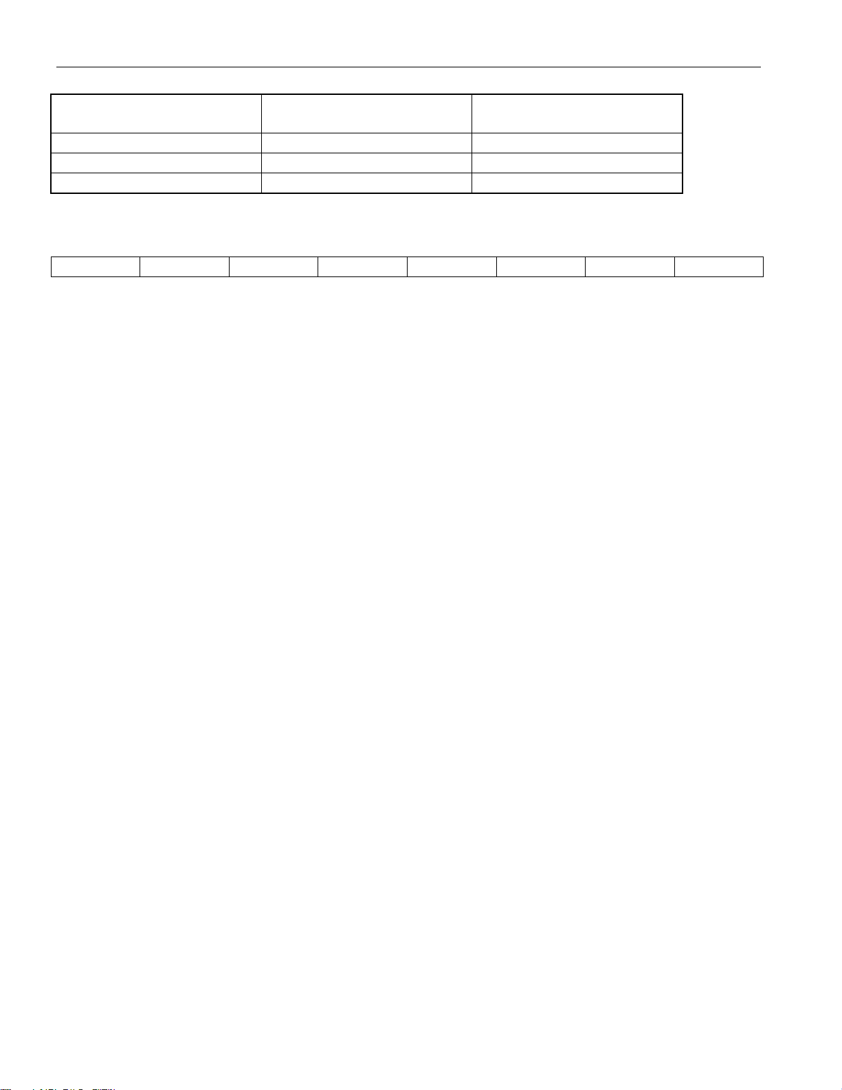
MCLK SELECTION Table 4-10
MCLK JAMUX
(CCR1.3)
2.048MHz 0 0
2.048MHz 1 1
1.544MHz 0 1
ETS
(CCR1.7)
20 of 75
Page 21

PARALLEL PORT MODE PINOUT (BIS1 = 0, BIS0 = 1 or 0) Figure 4-1
36 VDD
37 TRING
38 RPOS
39 RNEG
40 RCLK
41 TPOS
42 TNEG
43 TCLK
44 PBTS
34 TTIP
35 VSS
DS2148/Q48
1 CS*
2 RD (DS)
3 WR* (R/W*)
4 ALE (AS)
5 NA
6 NA
7 A4
8 A3
9 A2
10 A1
11 A0
AD7/D7 12
DS2148
Parallel Port
Operation
(Note: tie all NA pins low)
AD4/D4 15
AD5/D5 14
AD6/D6 13
AD3/D3 16
AD2/D2 17
AD1/D1 18
AD0/D0 19
VSM 20
VDD 21
t
i
e
h
i
g
h
BIS1 33
BIS0 32
BPCLK 31
MCLK 30
HRST* 29
RRING 28
RTIP 27
TEST 26
RCL/LOTC 25
PBEO 24
INT* 23
VSS 22
tie low
tie low (MUX) or high (non-MUX)
SERIAL PORT MODE PINOUT (BIS1 = 1, BIS0 = 0) Figure 4-2
t
i
e
l
o
w
34 TTIP
35 VSS
36 VDD
37 TRING
38 RPOS
39 RNEG
40 RCLK
41 TPOS
42 TNEG
43 TCLK
44 PBTS
1 CS*
2 NA
3 NA
4 NA
5 SCLK
6 SDI
7 SDO
8 ICES
9 OCES
10 NA
11 NA
BIS1 33
BIS0 32
BPCLK 31
MCLK 30
DS2148
Serial Port
Operation
(Note: tie all NA pins low)
VSM 20
NA 19
NA 18
NA 17
NA 16
NA 15
NA 14
NA 13
NA 12
t
i
e
h
i
g
h
RCL/LOTC 25
VDD 21
VSS 22
HRST* 29
RRING 28
RTIP 27
TEST 26
PBEO 24
INT* 23
tie high
tie low
21 of 75
Page 22

HARDWARE MODE PINOUT (BIS1 = 1, BIS0 = 1) Figure 4-3
44 RT0
43 TCLK
42 TNEG
40 RCLK
41 TPOS
38 RPOS
39 RNEG
36 VDD
37 TRING
34 TTIP
35 VSS
DS2148/Q48
1 EGL
2 ETS
3 NRZE
4 SCLKE
5 L2
6 L1
7 L0
8 DJA
9 JAMUX
10 JAS
11 HBE
DS2148
Hardware
Operation
LOOP1 17
LOOP0 16
CES 12
TPD 13
TX1 15
TX0 14
MM0 18
MM1 19
VSM 20
VDD 21
t
i
e
h
i
g
h
BIS1 33
BIS0 32
BPCLK 31
MCLK 30
HRST* 29
RRING 28
RTIP 27
TEST 26
RCL 25
PBEO 24
RT1 23
VSS 22
tie high
tie high
5. HARDWARE MODE
In hardware mode (BIS1 = 1, BIS0 = 1), pins 1-19, 23, 25, 31, and 44 are redefined to be used for
initializing the DS2148. BPCLK (pin 31) defaults to a 16.384MHz output when in hardware mode. The
RCL/LOTC (pin 25) is designated to RCL when in hardware mode. JABDS (CCR4.2) defaults to logic
0. The RHBE (CCR2.3) and THBE (CCR2.2) control bits are combined and controlled by HBE at pin 11
while the RSCLKE (CCR5.3) and TSCLKE (CCR5.2) bits are combined and controlled by SCLKE at
pin 4. TCES (CCR2.1) and RCES (CCR2.0) are combined and controlled by CES at pin 12. The
transmitter functions are combined and controlled by TX1 (pin 15) and TX0 (pin 14). LOOP1 (pin 17)
and LOOP0 (pin 16) control the loopback functions. All other control bits default to the logic 0 setting.
22 of 75
Page 23

DS2148/Q48
5.1 Register Map
REGISTER MAP Table 5-1
ACRONYM REGISTER NAME R/W PARALLEL
PORT MODE
CCR1 Common Control Register 1 R/W 00h B000 000A
CCR2 Common Control Register 2 R/W 01h B000 001A
CCR3 Common Control Register 3 R/W 02h B000 010A
CCR4 Common Control Register 4 R/W 03h B000 011A
CCR5 Common Control Register 5 R/W 04h B000 100A
CCR6 Common Control Register 6 R/W 05h B000 101A
SR Status Register R 06h B000 110A
IMR Interrupt Mask Register R/W 07h B000 111A
RIR1 Receive Information Register 1 R 08h B001 000A
RIR2 Receive Information Register 2 R 09h B001 001A
IBCC In-Band Code Control Register R/W 0Ah B001 010A
TCD1 Transmit Code Definition
R/W 0Bh B001 011A
Register 1
TCD2 Transmit Code Definition
R/W 0Ch B001 100A
Register 2
RUPCD1 Receive Up Code Definition
R/W 0Dh B001 101A
Register 1
RUPCD2 Receive Up Code Definition
R/W 0Eh B001 110A
Register 2
RDNCD1 Receive Down Code Definition
R/W 0Fh B001 111A
Register 1
RDNCD2 Receive Down Code Definition
R/W 10h B010 000A
Register 2
ECR1 Error Count Register 1 R 11h B010 001A
ECR2 Error Count Register 2 R 12h B010 010A
TEST1 Test 1 R/W 13h B010 011A
TEST2 Test 2 R/W 14h B010 100A
TEST3 Test 3 R/W 15h B010 101A
– – – Note 1 –
SERIAL
PORT MODE
See Notes 2–5
(msb) (lsb)
NOTES:
1) Register addresses 16h to 1Fh do not exist.
2) In the Serial Port Mode, the LSB is on the right hand side.
3) In the Serial Port Mode, data is read and written LSB first.
4) In the Serial Port Mode, the A bit (the LSB) determines whether the access is a read (A = 1) or a write
(A = 0).
5) In the Serial Port Mode, the B bit (the MSB) determines whether the access is a burst access (B = 1)
or a single register access (B = 0).
23 of 75
Page 24

DS2148/Q48
5.2 Parallel Port Operation
When using the parallel interface on the DS2148 (BIS1 = 0) the user has the option for either multiplexed
bus operation (BIS1 = 0, BIS0 = 0) or nonmultiplexed bus operation (BIS1 = 0, BIS0 = 1). The DS2148
can operate with either Intel or Motorola bus timing configurations. If the PBTS pin is tied low, Intel
timing will be selected; if tied high, Motorola timing will be selected. All Motorola bus signals are listed
in parenthesis (). See the timing diagrams in Section 12 for more details.
5.3 Serial Port Operation
Setting BIS1 = 1 and BIS0 = 0 enables the serial bus interface on the DS2148. Port read/write timing is
unrelated to the system transmit and receive timing, allowing asynchronous reads or writes by the host.
See Section 12 for the AC timing of the serial port. All serial port accesses are LSB first. See Figure 5-1,
Figure 5-2, Figure 5-3, and Figure 5-4 for more details.
Reading or writing to the internal registers requires writing one address/command byte prior to
transferring register data. The first bit written (LSB) of the address/command byte specifies whether the
access is a read (1) or a write (0). The next 5 bits identify the register address. Bit 7 is reserved and must
be set to 0 for proper operation.
The last bit (MSB) of the address/command byte is the burst mode bit. When the burst bit is enabled
(B = 1) and a READ operation is performed, addresses 0 through 15h are read sequentially, starting at
address 0h. And when the burst bit is enabled and a WRITE operation is performed, addresses 0 through
16h are written sequentially, starting at address 0h. Burst operation is stopped once address 15h is read.
See Figure 5-5 and Figure 5-6 for more details.
All data transfers are initiated by driving the CS* input low. When input clock-edge select (ICES) is low,
input data is latched on the rising edge of SCLK and when ICES is high, input data is latched on the
falling edge of SCLK. When output clock-edge select (OCES) is low, data is output on the falling edge of
SCLK and when OCES is high, data is output on the rising edge of SCLK. Data is held until the next
falling or rising edge. All data transfers are terminated if the CS* input transitions high. Port control logic
is disabled and SDO is 3-stated when CS* is high.
24 of 75
Page 25
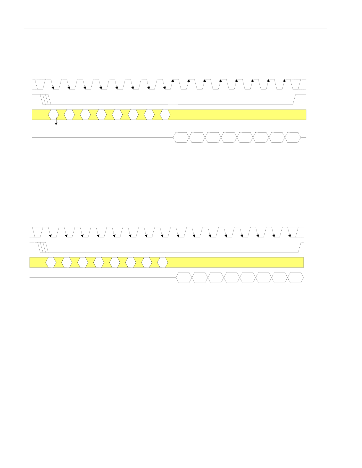
DS2148/Q48
K
SERIAL PORT OPERATION FOR READ ACCESS (R=1) MODE 1 Figure 5-1
ICES = 1 (sample SDI on the falling edge of SCLK)
OCES = 1 (update SDO on rising edge of SCLK)
SCL
123456 789
CS*
SDI
(lsb) (msb)
SDO
A0 A1 A2 A3 A4
1
READ ACCESS ENABLED
0B
10 11 12 13 14 15 16
D1 D2 D3 D4 D5 D6
D0
(lsb)
D7
(msb)
SERIAL PORT OPERATION FOR READ ACCESS MODE 2 Figure 5-2
ICES = 1 (sample SDI on the falling edge of SCLK)
OCES = 0 (update SDO on falling edge of SCLK)
SCLK
123456 789
10 11 12 13 14 15 16
CS*
SDI
SDO
A0 A1 A2 A3 A4
1
(lsb) (msb)
0B
D1 D2 D3 D4 D5 D6
D0
(lsb)
D7
(msb)
25 of 75
Page 26
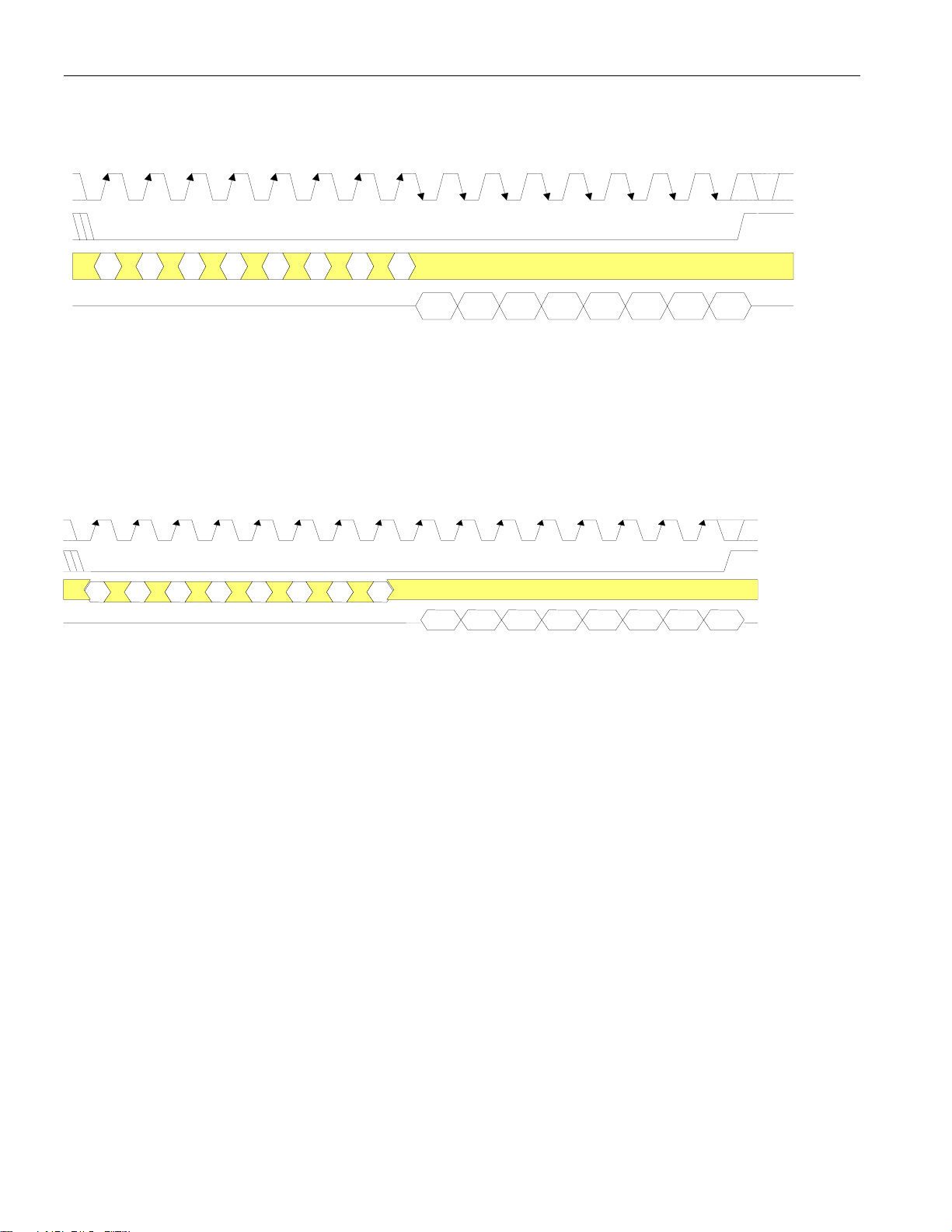
SERIAL PORT OPERATION FOR READ ACCESS MODE 3 Figure 5-3
K
A
K
ICES = 0 (sample SDI on the rising edge of SCLK)
OCES = 0 (update SDO on falling edge of SCLK)
SCL
123456 789
10 11 12 13 14 15 16
CS*
SDI
A0 A1 A2 A3 A4
1
(lsb) (msb)
SDO
0B
D1 D2 D3 D4 D5 D6
D0
(lsb)
D7
(msb)
SERIAL PORT OPERATION FOR READ ACCESS MODE 4 Figure 5-4
ICES = 0 (sample SDI on the rising edge of SCLK)
OCES = 1 (update SDO on rising edge of SCLK)
SCL
CS*
SDI
SDO
12345678 9
A0 A1 A2 A3
1
(lsb) (msb)
4
B
0
10 11 12 13 14 15 16
D1 D2 D3 D4 D5 D6D0 D7
(lsb)
(msb)
DS2148/Q48
D0D0D0D0D0D0D0D0D0D0D0D0D0D0D0D0D0D0D0D0D0D0D0D0D0D0D0D0D0D0D0D0D0D0
D0D0D0D0D0D0
D0
26 of 75
Page 27
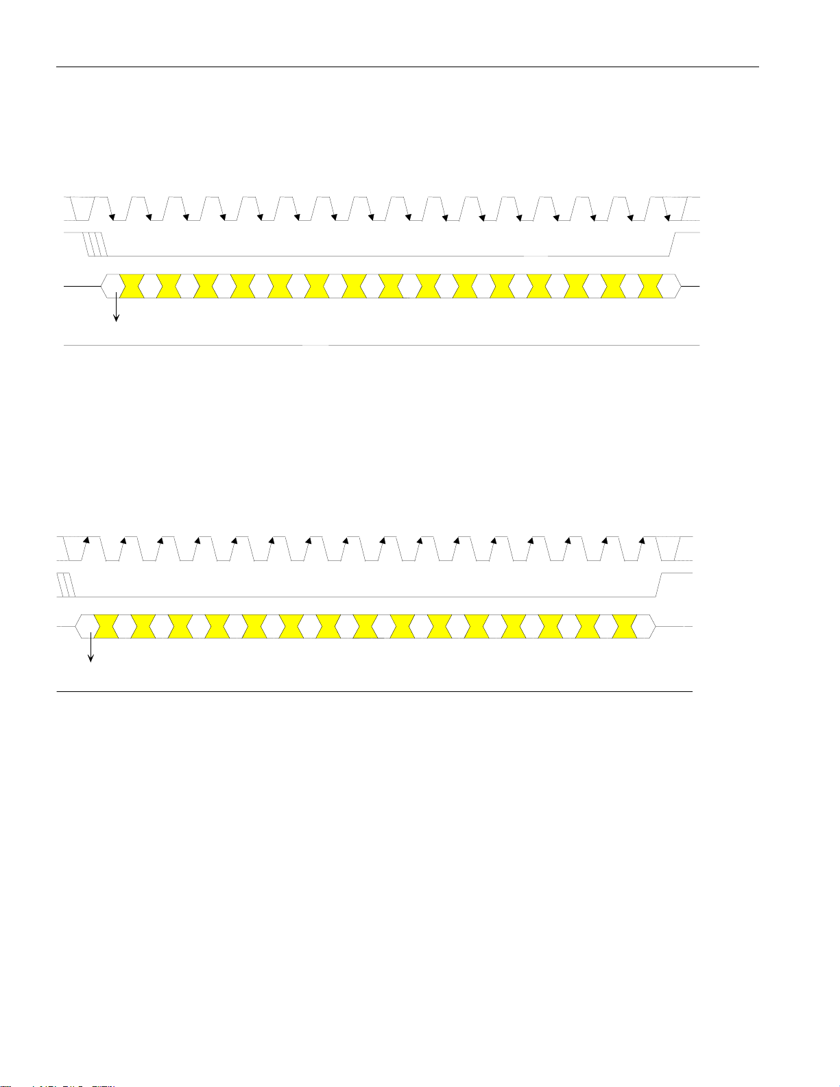
SERIAL PORT OPERATION FOR WRITE ACCESS (R=0) Figure 5-5
A
MODES 1 and 2
ICES = 1 (sample SDI on the falling edge of SCLK)
SCLK
CS*
1234 56789
10 11 12 13 14 15 16
SDI
(lsb)
WRITE ACCESS ENABLED
SDO
A0 A1 A2 A3 A4
0
0B
(msb)
DO
D1 D2 D3 D4 D5 D7
(lsb) (msb)
D6
SERIAL PORT OPERATION FOR WRITE ACCESS (R=0) Figure 5-6
DS2148/Q48
MODES 3 and 4
ICES = 0 (sample SDI on the rising edge of SCLK)
123456789
CS*
SDI
0
(lsb)
WRITE ACCESS EN ABLED
SDO
0A1A2A3A4
0B
(msb)
DO
(lsb) (msb)
10 11 12 13 14 15 16SCLK
D1 D2 D3 D4 D5 D7
D6
27 of 75
Page 28

DS2148/Q48
6. CONTROL REGISTERS
CCR1 (00H): COMMON CONTROL REGISTER 1
(MSB)
ETS NRZE RCLA ECUE JAMUX TTOJ TTOR LOTCMC
SYMBOL POSITION DESCRIPTION
ETS CCR1.7
NRZE CCR1.6
RCLA CCR1.5
ECUE CCR1.4 Error Counter Update Enable. A 0 to 1-transition forces the
JAMUX CCR1.3 Jitter Attenuator MUX. Controls the source for JACLK. See
TTOJ CCR1.2 TCLK to JACLK. Internally connects TCLK to JACLK. See
TTOR CCR1.1 TCLK to RCLK. Internally connects TCLK to RCLK. See
LOTCMC CCR1.0 Loss Of Transmit Clock Mux Control. Determines whether
(LSB)
E1/T1 Select.
0 = E1
1 = T1
NRZ Enable.
0 = Bipolar data at RPOS/RNEG and TPOS/TNEG
1 = NRZ data at RPOS and TPOS or TNEG; RNEG outputs a
positive going pulse when device receives a BPV, CV, or EXZ.
See figure 3-2 and figure 3-3.
Receive Carrier Loss Alternate Criteria.
0 = RCL declared upon 255 (E1) or 192 (T1) consecutive zeros
1 = RCL declared upon 2048 (E1) or 1544 (T1) consecutive
zeros
next clock cycle to load the error counter registers with the
latest counts and reset the counters. The user must wait a
minimum of two clocks cycles (976ns for E1 and 1296ns for
T1) before reading the error count registers to allow for a proper
update. See Section 6 and figure 3-2 for details.
Figure 3-1.
0 = JACLK sourced from MCLK (2.048MHz or 1.544MHz at
MCLK)
1 = JACLK sourced from internal PLL (2.048MHz at MCLK)
figure 3-3.
0 = disabled
1 = enabled
figure 3-3.
0 = disabled
1 = enabled
the transmit logic should switch to JACLK if the TCLK input
should fail to transition. See figure 3-3.
0 = do not switch to JACLK if TCLK stops
1 = switch to JACLK if TCLK stops
28 of 75
Page 29
DS2148/Q48
MCLK SELECTION Table 6-1
MCLK JAMUX
(CCR1.3)
2.048MHz 0 0
2.048MHz 1 1
1.544MHz 0 1
ETS
(CCR1.7)
CCR2 (01H): COMMON CONTROL REGISTER 2
(MSB)
P25S N/A SCLD CLDS RHBE THBE TCES RCES
SYMBOL POSITION DESCRIPTION
P25S CCR2.7 Pin 25 Select. Forced to logic 0 in hardware mode.
- CCR2.6
SCLD CCR2.5 Short Circuit Limit Disable (ETS = 0). Controls the 50mA
CLDS CCR2.4 Custom Line Driver Select. Setting this bit to a one will
RHBE CCR2.3 Receive HDB3/B8ZS Enable. See figure 3-2.
THBE CCR2.2 Transmit HDB3/B8ZS Enable. See figure 3-3.
TCES CCR2.1 Transmit Clock Edge Select. Selects which TCLK edge to
RCES CCR2.0 Receive Clock Edge Select. Selects which RCLK edge to
0 = toggles high during a Receive Carrier Loss condition
1 = toggles high if TCLK does not transition for at least 5ms.
Not Assigned. Should be set to zero when written to.
(rms) current limiter.
0 = enable 50mA current limiter
1 = disable 50mA current limiter
redefine the operation of the transmit line driver. When this bit
is set to a one and CCR4.5 = CCR4.6 = CCR4.7 = 0, then the
device will generate a square wave at the TTIP and TRING
outputs instead of a normal waveform. When this bit is set to a
one and CCR4.5 = CCR4.6 = CCR4.7 ¹ 0, then the device will
force TTIP and TRING outputs to become open drain drivers
instead of their normal push-pull operation. This bit should be
set to zero for normal operation of the device. Contact the
factory for more details on how to use this bit.
0 = enable HDB3 (E1)/B8ZS (T1)
1 = disable HDB3 (E1)/B8ZS (T1)
0 = enable HDB3 (E1)/B8ZS (T1)
1 = disable HDB3 (E1)/B8ZS (T1)
sample TPOS and TNEG. See figure 3-3.
0 = sample TPOS and TNEG on falling edge of TCLK
1 = sample TPOS and TNEG on rising edge of TCLK
update RPOS and RNEG. See figure 3-2.
0 = update RPOS and RNEG on rising edge of RCLK
1 = update RPOS and RNEG on falling edge of RCLK
(LSB)
29 of 75
Page 30

DS2148/Q48
CCR3 (02H): COMMON CONTROL REGISTER 3
(MSB)
TUA1 ATUA1 TAOZ TPRBSE TLCE LIRST IBPV IBE
SYMBOL POSITION DESCRIPTION
TUA1 CCR3.7 Transmit Unframed All Ones. The polarity of this bit is set
ATUA1 CCR3.6 Automatic Transmit Unframed All Ones. Automatically
TAOZ CCR3.5 Transmit Alternate Ones and Zeros. Transmit a …101010…
TPRBSE CCR3.4 Transmit PRBS Enable. Transmit a 215 - 1 (E1) or a 220 - 1
TLCE CCR3.3 Transmit Loop Code Enable. Enables the transmit side to
LIRST CCR3.2 Line Interface Reset. Setting this bit from a zero to a one will
IBPV CCR3.1 Insert BPV. A 0 to 1 transition on this bit will cause a single
IBE CCR3.0 Insert Bit Error. A 0 to 1 transition on this bit will cause a
(LSB)
such that the device will transmit an all ones pattern on powerup or device reset. This bit must be set to a one to allow the
device to transmit data. The transmission of this data pattern is
always timed off of the JACLK (See Figure 3-1).
0 = transmit all ones at TTIP and TRING
1 = transmit data normally
transmit an unframed all ones pattern at TTIP and TRING
during a receive carrier loss (RCL) condition or a receive all
ones condition.
0 = disabled
1 = enabled
pattern at TTIP and TRING. The transmission of this data
pattern is always timed off of TCLK (Figure 3-1).
0 = disabled
1 = enabled
(T1) PRBS at TTIP and TRING. See figure 3-3.
0 = disabled
1 = enabled
transmit the loop up code in the Transmit Code Definition
registers (TCD1 and TCD2). See Section 6 and figure 3-3 for
details.
0 = disabled
1 = enabled
initiate an internal reset that resets the clock recovery state
machine and re-centers the jitter attenuator. Normally this bit is
only toggled on power-up. Must be cleared and set again for a
subsequent reset.
BiPolar Violation (BPV) to be inserted into the transmit data
stream. Once this bit has been toggled from a 0 to a 1, the
device waits for the next occurrence of three consecutive ones
to insert the BPV. This bit must be cleared and set again for a
subsequent error to be inserted. See figure 3-3.
single logic error to be inserted into the transmit data stream.
This bit must be cleared and set again for a subsequent error to
be inserted. See Figure 3-3.
30 of 75
Page 31
DS2148/Q48
6.1 Device Power-Up And Reset
The DS2148 will reset itself upon power-up, setting all writeable registers to 00h and clearing the status
and information registers. CCR3.7 (TUA1) = 0 results in the LIU transmitting unframed all ones. After
the power supplies have settled following power-up, initialize all control registers to the desired settings,
then toggle the LIRST bit (CCR3.2). The DS2148 can be reset at anytime to the default settings by
bringing HRST* (pin 29) low (level triggered) or by powering down and powering up again.
CCR4 (03H): COMMON CONTROL REGISTER 4
(MSB)
L2 L1 L0 EGL JAS JABDS DJA TPD
SYMBOL POSITION DESCRIPTION
L2 CCR4.7 Line Build Out Select Bit 2. Sets the transmitter build out
L1 CCR4.6 Line Build Out Select Bit 1. Sets the transmitter build out
L0 CCR4.5 Line Build Out Select Bit 0. Sets the transmitter build out
EGL CCR4.4 Receive Equalizer Gain Limit. This bit controls the sensitivity
JAS CCR4.3
JABDS CCR4.2
DJA CCR4.1
TPD CCR4.0
(Table 9-1 for E1 and Table 9-2 for T1)
(Table 9-1 for E1 and Table 9-2 for T1)
(Table 9-1 for E1 and Table 9-2 for T1)
of the receive equalizer (Table 6-2)
Jitter Attenuator Select.
0 = place the jitter attenuator on the receive side
1 = place the jitter attenuator on the transmit side
Jitter Attenuator Buffer Depth Select.
0 = 128 bits
1 = 32 bits (use for delay sensitive applications)
Disable Jitter Attenuator.
0 = jitter attenuator enabled
1 = jitter attenuator disabled
Transmit Power-Down.
0 = normal transmitter operation
1 = powers down the transmitter and 3-states the TTIP and
TRING pins
(LSB)
RECEIVE SENSITIVITY SETTINGS Table 6-2
EGL
(CCR4.4)
0 0 (E1) -12dB (short haul)
1 0 (E1) -43dB (long haul)
1 1 (T1) -30dB (limited long haul)
0 1 (T1) -36dB (long haul)
ETS
(CCR1.7)
RECEIVE SENSITIVITY
31 of 75
Page 32
DS2148/Q48
CCR5 (04H): COMMON CONTROL REGISTER 5
(MSB)
BPCS1 BPCS0 MM1 MM0 RSCLKE TSCLKE RT1 RT0
SYMBOL POSITION DESCRIPTION
BPCS1 CCR5.7 Back Plane Clock Select 1. See Table 6-3 for details.
BPCS0 CCR5.6 Back Plane Clock Select 0. See Table 6-3 for details.
MM1 CCR5.5 Monitor Mode 1. See Table 6-4.
MM0 CCR5.4 Monitor Mode 0. See Table 6-4.
RSCLKE CCR5.3
TSCLKE CCR5.2
RT1 CCR5.1 Receive Termination 1. See Table 6-5 for details.
RT0 CCR5.0 Receive Termination 0. See Table 6-5 for details.
Receive Synchronization Clock Enable.
This control bit determines whether the line receiver should
handle normal T1/E1 signals or a synchronized signal.
E1 mode:
0 = receive normal E1 signal (Section 6 of G.703)
1 = receive 2.048 MHz synchronization signal (section 10 of
G.703)
T1 mode:
0 = receive normal T1 signal
1 = receive 1.544 MHz synchronization signal
Transmit Synchronization Clock Enable.
This control bit determines whether the transmitter should
transmit normal T1/E1 signals or a synchronized signal.
E1 mode:
0 = transmit normal E1 signal (section 6 of G.703)
1 = transmit 2.048 MHz synchronization signal (section 10 of
G.703)
T1 mode:
0 = transmit normal T1 signal
1 = transmit 1.544 MHz synchronization signal
(LSB)
BACK PLANE CLOCK SELECT Table 6-3
BPCS1
(CCR5.7)
0 0 16.384MHz
0 1 8.192MHz
1 0 4.096MHz
1 1 2.048MHz
BPCS0
(CCR5.6)
BPCLK FREQUENCY
MONITOR GAIN SETTINGS Table 6-4
32 of 75
Page 33

DS2148/Q48
MM1
(CCR5.5)
MM0
(CCR5.4)
INTERNAL LINEAR
GAIN BOOST (dB)
0 0 Normal operation (no boost)
0 1 20
1 0 26
1 1 32
33 of 75
Page 34
DS2148/Q48
INTERNAL RX TERMINATION SELECT Table 6-5
RT1
(CCR5.1)
0 0 Internal receive-side termination disabled
0 1
1 0
1 1
RT0
(CCR5.0)
INTERNAL RECEIVE
TERMINATION CONFIGURATION
Internal receive-side 120W enabled
Internal receive-side 100W enabled
Internal receive-side 75W enabled
CCR6 (05H): COMMON CONTROL REGISTER 6
(MSB)
LLB RLB ARLBE ALB RJAB ECRS2 ECRS1 ECRS0
SYMBOL POSITION DESCRIPTION
LLB CCR6.7 Local Loopback. In Local Loopback (LLB), transmit data will
RLB CCR6.6 Remote Loopback. In Remote Loopback (RLB), data output
ARLBE CCR6.5 Automatic Remote Loopback Enable and Reset. When this
ALB CCR6.4 Analog Loopback. In analog loopback (ALB), signals at TTIP
34 of 76
be looped back to the receive path passing through the jitter
attenuator if it is enabled. Data in the transmit path will act as
normal. See Figure 3-1 (DS2148 BLOCK DIAGRAM Figure
3-1 and section 8-2.2 for details.
0 = loopback disabled
1 = loopback enabled
from the clock/data recovery circuitry will be looped back to the
transmit path passing through the jitter attenuator if it is
enabled. Data in the receive path will act as normal while data
presented at TPOS and TNEG will be ignored. See Figure 3-1
(DS2148 BLOCK DIAGRAM Figure 3-1 and section 8-2.1 for
details.
0 = loopback disabled
1 = loopback enabled
bit is set high, the device will automatically go into remote
loopback when it detects loop-up code programmed into the
receive loop-up code definition registers (RUPCD1 and
RUPCD2) for a minimum of 5 seconds and it will also set the
RIR2.1 status bit. Once in a RLB state, it will remain in this
state until it has detected the loop code programmed into the
receive loop-down code definition registers (RDNCD1 and
RDNCD2) for a minimum of 5 seconds at which point it will
force the device out of RLB and clear RIR2.1. Toggling this bit
from a 1 to a 0 can reset the automatic RLB circuitry. The
action of the automatic remote loopback circuitry is logically
OR’ed with the RLB (CCR6.6) control bit (i.e., either one can
cause a RLB to occur).
and TRING will be internally connected to RTIP and RRING.
The incoming signals, from the line, at RTIP and RRING will
be ignored. The signals at TTIP and TRING will be transmitted
as normal. See Figure 3-1 (DS2148 BLOCK DIAGRAM
(LSB)
Page 35

DS2148/Q48
SYMBOL POSITION DESCRIPTION
Figure 3-1 and section 8-2.3 for more details.
0 = loopback disabled
1 = loopback enabled
RJAB CCR6.3 RCLK Jitter Attenuator Bypass. This control bit allows the
recovered received clock and data to bypass the jitter
attenuation while still allowing the BPCLK output to use the
jitter attenuator. See Figure 3-1 and section 9-1 for details.
0 = disabled
1 = enabled
ECRS2 CCR6.2 Error Count Register Select 2. See Section 8.4 for details.
ECRS1 CCR6.1 Error Count Register Select 1. See Section 8.4 for details.
ECRS0 CCR6.0 Error Count Register Select 0. See Section 8.4 for details.
7. STATUS REGISTERS
There are three registers that contain information on the current real-time status of the device, status
register (SR), and receive information registers 1 and 2 (RIR1/RIR2). When a particular event has
occurred (or is occurring), the appropriate bit in one of these three registers will be set to a one. Some of
the bits in SR, RIR1, and RIR2 are latched bits and some are real-time bits. The register descriptions
below list which status bits are latched and which are real-time bits. For latched status bits, when an event
or an alarm occurs the bit is set to a one and will remain set until the user reads that bit. The bit will be
cleared when it is read and it will not be set again until the event has occurred again. Two of the latched
status bits (RUA1 & RCL) will remain set after reading if the alarm is still present.
The user will always precede a read of any of the three status registers with a write. The byte written to
the register will inform the DS2148 which bits the user wishes to read and have cleared. The user will
write a byte to one of these registers with a one in the bit positions to be read and a zero in the other bit
positions. When a one is written to a bit location, that location will be updated with the latest information.
When a zero is written to a bit position, that bit position will not be updated and the previous value will
be held. A write to the status and information registers will be immediately followed by a read of the
same register. The read result should be logically AND’ed with the mask byte that was just written and
this value should be written back into the same register to ensure that bit does indeed clear. This second
write step is necessary because the alarms and events in the status registers occur asynchronously with
respect to their access via the parallel port. This write-read-write scheme allows an external
microcontroller or microprocessor to individually poll certain bits without disturbing the other bits in the
register. This operation is key in controlling the DS2148 with higher-order software languages.
The bits in the SR register have the unique ability to initiate a hardware interrupt via the INT* output pin.
Each of the alarms and events in the SR can be either masked or unmasked from the interrupt pin via the
interrupt mask register (IMR). The interrupts caused by the RCL, RUA1, and LOTC bits in SR act
differently than the interrupts caused by the other status bits in SR. The RCL, RUA1 and LOTC bits will
force the INT* pin low whenever they change state (i.e., go active or inactive). The INT* pin will be
allowed to return high (if no other interrupts are present) when the user reads the alarm bit that caused the
interrupt to occur even if the alarm is still present. The other status bits in SR can force the INT* pin low
when they are set. The INT* pin will be allowed to return high (if no other interrupts are present) when
the user reads the event bit that caused the interrupt to occur.
35 of 76
Page 36
DS2148/Q48
RECEIVED ALARM CRITERIA Table 7-1
ALARM E1/T1 SET CRITERIA CLEAR CRITERIA
RUA1 E1 Less than two zeros in two
frames (512 bits)
RUA1 T1 Over a 3ms window, five or less
zeros are received
1
RCL
E1 255 (or 2048)2 consecutive zeros
received
More than two zeros in two
frames (512 bits)
Over a 3ms window, six or more
zeros are received
In 255 bit times, at least 32 ones
are received
(G.775)
1
RCL
T1 192 (or 1544)2 consecutive zeros
are received
14 or more ones out of 112
possible bit positions are
received starting with the first
one received
NOTES:
1) Receive carrier loss (RCL) is also known as loss-of-signal (LOS) or Red Alarm in T1.
2) See CCR1.5 for details.
SR (06H): STATUS REGISTER
(MSB)
LUP LDN LOTC RUA1 RCL TCLE TOCD PRBSD
SYMBOL POSITION DESCRIPTION
LUP
(latched)
LDN
(latched)
LOTC
(real time)
RUA1
(latched)
RCL
(latched)
TCLE
(real time)
TOCD
(real time)
PRBSD
(real time)
(LSB)
SR.7 Loop Up Code Detected. Set when the loop up code defined in
registers RUPCD1 and RUPCD2 is being received. See Section
6 for details.
SR.6 Loop Down Code Detected. Set when the loop down code
defined in registers RDNCD1 and RDNCD2 is being received.
See Section 6 for details.
SR.5 Loss of Transmit Clock. Set when the TCLK pin has not
transitioned for 5msec (±2msec). Will force the LOTC pin high.
SR.4 Receive Unframed All Ones. Set when an unframed all ones
code is received at RRING and RTIP. See Table 7-1for details.
SR.3 Receive Carrier Loss. Set when a receive carrier loss condition
exists at RRING and RTIP. See Table 7-1for details.
SR.2 Transmit Current Limit Exceeded. Set when the 50mA (rms)
current limiter is activated whether the current limiter is enabled
or not.
SR.1 Transmit Open Circuit Detect. Set when the device detects
that the TTIP and TRING outputs are open circuited.
SR.0 PRBS Detect. Set when the receive-side detects a 215-1 (E1) or
20
-1 (T1) Pseudo Random Bit Sequence (PRBS).
a 2
36 of 75
Page 37

DS2148/Q48
IMR (07H): INTERRUPT MASK REGISTER
(MSB)
LUP LDN LOTC RUA1 RCL TCLE TOCD PRBSD
SYMBOL POSITION DESCRIPTION
LUP IMR.7
LDN IMR.6
LOTC IMR.5
RUA1 IMR.4
RCL IMR.3
TCLE IMR.2
TOCD IMR.1
PRBSD IMR.0
(LSB)
Loop Up Code Detected.
0 = interrupt masked
1 = interrupt enabled
Loop Down Code Detected.
0 = interrupt masked
1 = interrupt enabled
Loss of Transmit Clock.
0 = interrupt masked
1 = interrupt enabled
Receive Unframed All Ones.
0 = interrupt masked
1 = interrupt enabled
Receive Carrier Loss.
0 = interrupt masked
1 = interrupt enabled
Transmit Current Limiter Exceeded.
0 = interrupt masked
1 = interrupt enabled
Transmit Open Circuit Detect.
0 = interrupt masked
1 = interrupt enabled
PRBS Detection.
0 = interrupt masked
1 = interrupt enabled
37 of 75
Page 38

DS2148/Q48
RIR1 (08H): RECEIVE INFORMATION REGISTER 1
(MSB)
ZD 16ZD HBD RCLC RUA1C JALT N/A N/A
SYMBOL POSITION DESCRIPTION
ZD
(latched)
16ZD
(latched)
HBD
(latched)
RCLC
(latched)
RUA1C
(latched)
JALT
(latched)
N/A RIR1.1 Not Assigned. Could be any value when read.
N/A RIR1.0 Not Assigned. Could be any value when read.
(LSB)
RIR1.7 Zero Detect. Set when a string of at least four (ETS = 0) or
eight (ETS = 1) consecutive zeros (regardless of the length of
the string) have been received. Will be cleared when read.
RIR1.6 Sixteen Zero Detect. Set when at least 16 consecutive zeros
(regardless of the length of the string) have been received. Will
be cleared when read.
RIR1.5 HDB3/B8ZS Word Detect. Set when an HDB3 (ETS = 0) or
B8ZS (ETS = 1) code word is detected independent of whether
the receive HDB3/B8ZS mode (CCR4.6) is enabled. Will be
cleared when read. Useful for automatically setting the line
coding.
RIR1.4 Receive Carrier Loss Clear. Set when the RCL alarm has met
the clear criteria defined in Table 7-1. Will be cleared when
read.
RIR1.3 Receive Unframed All Ones Clear. Set when the unframed all
ones signal is no longer detected. Will be cleared when read.
See Table 7-1.
RIR1.2 Jitter Attenuator Limit Trip. Set when the jitter attenuator
FIFO reaches to within 4 bits of its useful limit. Will be cleared
when read. Useful for debugging jitter attenuation operation.
38 of 75
Page 39
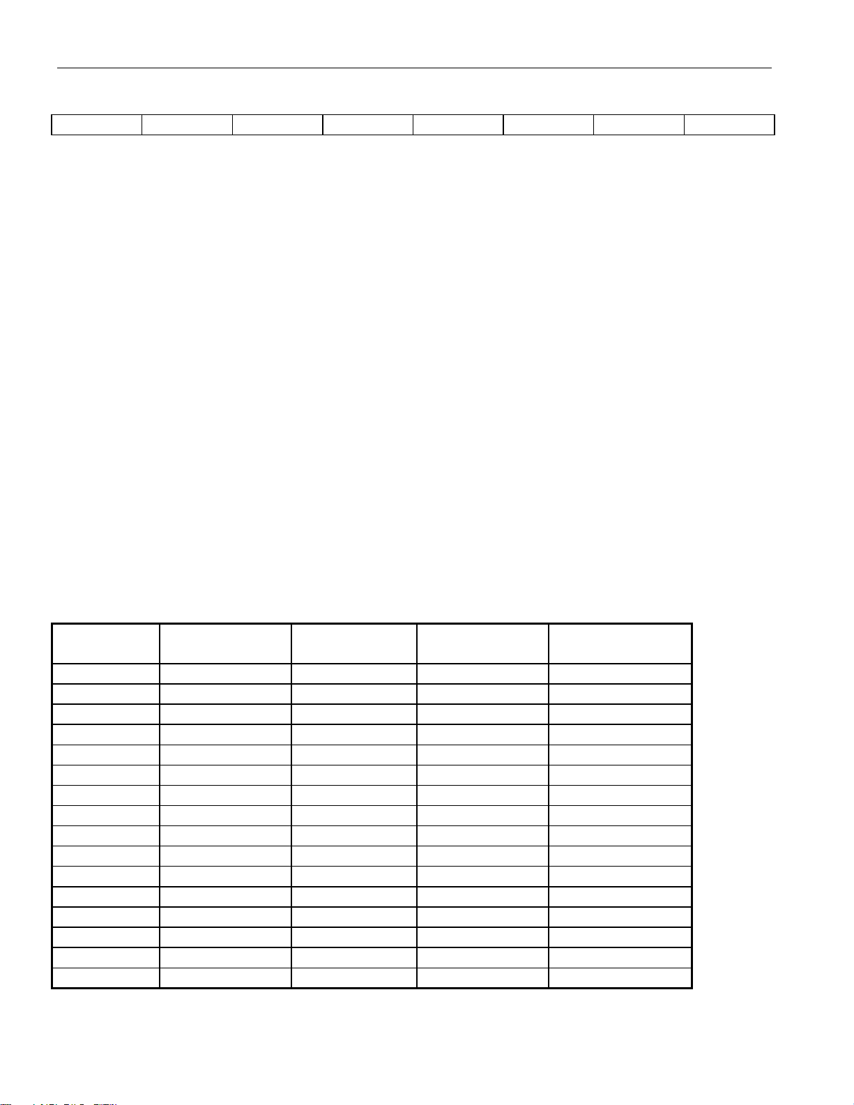
DS2148/Q48
RIR2 (09H): RECEIVE INFORMATION REGISTER 2
(MSB)
RL3 RL2 RL1 RL0 N/A N/A ARLB SEC
SYMBOL POSITION DESCRIPTION
RL3
(real time)
RL2
(real time)
RL1
(real time)
RL0
(real time)
N/A RIR2.3 Not Assigned. Could be any value when read.
N/A RIR2.2 Not Assigned. Could be any value when read.
ARLB
(real time)
SEC
(latched)
RIR2.7 Receive Level Bit 3. See Table 7-2.
RIR2.6 Receive Level Bit 2. See Table 7-2.
RIR2.5 Receive Level Bit 1. See Table 7-2.
RIR2.4 Receive Level Bit 0. See Table 7-2.
RIR2.1 Automatic Remote Loopback Detected. This bit will be set to
a one when the automatic Remote Loopback (RLB) circuitry
has detected the presence of a loop up code for 5 seconds. It
will remain set until the automatic RLB circuitry has detected
the loop down code for 5 seconds. See Section 6 for more
details. This bit will be forced low when the automatic RLB
circuitry is disabled (CCR6.5 = 0).
RIR2.0 One-Second Timer. This bit will be set to a one on one-second
boundaries as timed by the device based on the RCLK. It will
be cleared when read.
(LSB)
RECEIVE LEVEL INDICATION Table 7-2
RL3 RL2 RL1 RL0 Receive Level
(dB)
0 0 0 0 < -2.5
0 0 0 1 -2.5 to -5.0
0 0 1 0 -5.0 to -7.5
0 0 1 1 -7.5 to -10.0
0 1 0 0 -10.0 to -12.5
0 1 0 1 -12.5 to -15.0
0 1 1 0 -15.0 to -17.5
0 1 1 1 -17.5 to -20.0
1 0 0 0 -20.0 to -22.5
1 0 0 1 -22.5 to -25.0
1 0 1 0 -25.0 to -27.5
1 0 1 1 -27.5 to -30.0
1 1 0 0 -30.0 to -32.5
1 1 0 1 -32.5 to -35.0
1 1 1 0 -35.0 to -37.5
1 1 1 1 > -37.5
39 of 75
Page 40

DS2148/Q48
8. DIAGNOSTICS
8.1 In-Band Loop Code Generation and Detection
The DS2148 has the ability to generate and detect a repeating bit pattern that is from one to eight or
sixteen bits in length. To transmit a pattern, the user will load the pattern to be sent into the Transmit
Code Definition (TCD1 and TCD2) registers and select the proper length of the pattern by setting the
TC0 and TC1 bits in the In-Band Code Control (IBCC) register. When generating a 1, 2, 4, 8, or 16 bit
pattern both the transmit code registers (TCD1 and TCD2) must be filled with the proper code.
Generation of a 1, 3, 5, or 7-bit pattern only requires TCD1 to be filled. Once this is accomplished, the
pattern will be transmitted as long as the TLCE control bit (CCR3.3) is enabled. As an example, if the
user wished to transmit the standard “loop up” code for Channel Service Units which is a repeating
pattern of ...10000100001... then 80h would be loaded into TCD1 and the length would set using TC1 and
TC0 in the IBCC register to 5 bits.
The DS2148 can detect two separate repeating patterns to allow for both a loop-up code and a loop-down
code to be detected. The user will program the codes to be detected in the Receive Up Code Definition
(RUPCD1 and RUPCD2) registers and the Receive Down Code Definition (RDNCD1 and RDNCD2)
registers and the length of each pattern will be selected via the IBCC register. The DS2148 will detect
repeating pattern codes with bit error rates as high as 1x10⁻². The code detector has a nominal integration
period of 48ms, hence, after about 48ms of receiving either code, the proper status bit (LUP at SR.7 and
LDN at SR.6) will be set to a one. Normally codes are sent for a period of 5 seconds. It is recommended
that the software poll the DS2148 every 100ms to 1000ms until 5 seconds has elapsed to ensure that the
code is continuously present.
IBCC (0AH): IN–BAND CODE CONTROL REGISTER
(MSB)
TC1 TC0 RUP2 RUP1 RUP0 RDN2 RDN1 RDN0
SYMBOL POSITION DESCRIPTION
TC1 IBCC.7 Transmit Code Length Definition Bit 1. See Table 8-1
TC0 IBCC.6 Transmit Code Length Definition Bit 0. See Table 8-1
RUP2 IBCC.5 Receive Up Code Length Definition Bit 2. See Table 8-2
RUP1 IBCC.4 Receive Up Code Length Definition Bit 1. See Table 8-2
RUP0 IBCC.3 Receive Up Code Length Definition Bit 0. See Table 8-2
RDN2 IBCC.2 Receive Down Code Length Definition Bit 2. See Table 8-2
RDN1 IBCC.1 Receive Down Code Length Definition Bit 1. See Table 8-2
RDN0 IBCC.0 Receive Down Code Length Definition Bit 0. See Table 8-2
(LSB)
40 of 75
Page 41
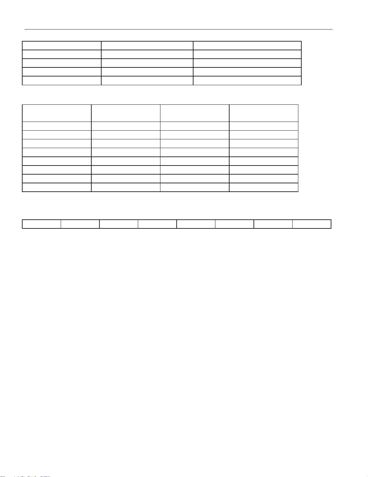
DS2148/Q48
TRANSMIT CODE LENGTH Table 8-1
TC1 TC0 LENGTH SELECTED
0 0 5 bits
0 1 6 bits / 3 bits
1 0 7 bits
1 1 16 bits / 8 bits/4 bits / 2 bits / 1 bits
RECEIVE CODE LENGTH Table 8-2
RUP2/ RDN2 RUP1/ RDN1 RUP0/ RDN0 LENGTH
SELECTED
0 0 0 1 bits
0 0 1 2 bits
0 1 0 3 bits
0 1 1 4 bits
1 0 0 5 bits
1 0 1 6 bits
1 1 0 7 bits
1 1 1 16 bits/8 bits
TCD1 (0BH): TRANSMIT CODE DEFINITION REGISTER 1
(MSB)
C7 C6 C5 C4 C3 C2 C1 C0
SYMBOL POSITION DESCRIPTION
C7 TCD1.7 Transmit Code Definition Bit 7. First bit of the repeating
C6 TCD1.6
C5 TCD1.5
C4 TCD1.4
C3 TCD1.3
C2 TCD1.2 Transmit Code Definition Bit 2. A Don’t Care if a 5-bit
C1 TCD1.1 Transmit Code Definition Bit 1. A Don’t Care if a 5 or 6 bit
C0 TCD1.0 Transmit Code Definition Bit 0. A Don’t Care if a 5, 6 or 7
pattern.
Transmit Code Definition Bit 6.
Transmit Code Definition Bit 5.
Transmit Code Definition Bit 4.
Transmit Code Definition Bit 3.
length is selected.
length is selected.
bit length is selected.
(LSB)
41 of 75
Page 42
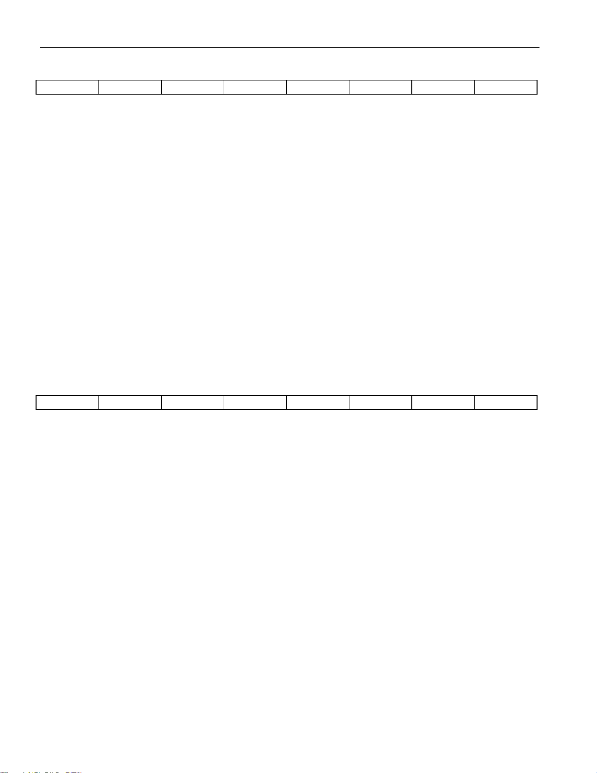
DS2148/Q48
TCD2 (0CH): TRANSMIT CODE DEFINITION REGISTER 2
(MSB)
C15 C14 C13 C12 C11 C10 C9 C8
SYMBOL POSITION DESCRIPTION
C15 TCD2.7
C14 TCD2.6
C13 TCD2.5
C12 TCD2.4
C11 TCD2.3
C10 TCD2.2
C9 TCD2.1
C8 TCD2.0
Transmit Code Definition Bit 15
Transmit Code Definition Bit 14
Transmit Code Definition Bit 13
Transmit Code Definition Bit 12
Transmit Code Definition Bit 11
Transmit Code Definition Bit 10
Transmit Code Definition Bit 9
Transmit Code Definition Bit 8
(LSB)
RUPCD1 (0DH): RECEIVE UP CODE DEFINITION REGISTER 1
(MSB)
C7 C6 C5 C4 C3 C2 C1 C0
SYMBOL POSITION DESCRIPTION
C7 RUPCD1.7 Receive Up Code Definition Bit 7. First bit of the repeating
C6 RUPCD1.6 Receive Up Code Definition Bit 6. A Don’t Care if a 1-bit
C5 RUPCD1.5 Receive Up Code Definition Bit 5. A Don’t Care if a 1 or 2
C4 RUPCD1.4 Receive Up Code Definition Bit 4. A Don’t Care if a 1 to 3
C3 RUPCD1.3 Receive Up Code Definition Bit 3. A Don’t Care if a 1 to 4
C2 RUPCD1.2 Receive Up Code Definition Bit 2. A Don’t Care if a 1 to 5
C1 RUPCD1.1 Receive Up Code Definition Bit 1. A Don’t Care if a 1 to 6
C0 RUPCD1.0 Receive Up Code Definition Bit 0. A Don’t Care if a 1 to 7
pattern.
length is selected.
bit length is selected.
bit length is selected.
bit length is selected.
bit length is selected.
bit length is selected.
bit length is selected.
(LSB)
42 of 75
Page 43
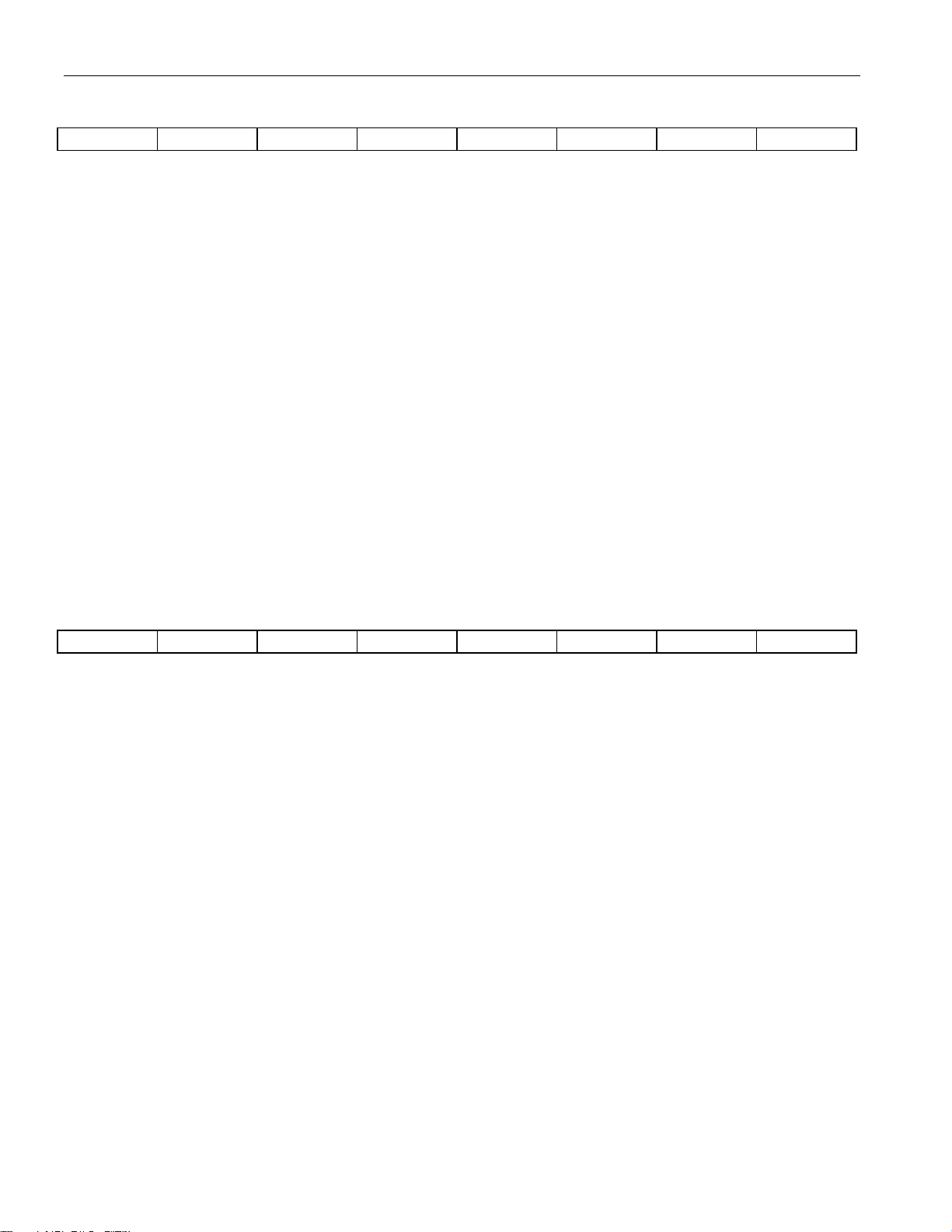
DS2148/Q48
RUPCD2 (0EH): RECEIVE UP CODE DEFINITION REGISTER 2
(MSB)
C15 C14 C13 C12 C11 C10 C9 C8
SYMBOL POSITION DESCRIPTION
C15 RUPCD2.7
C14 RUPCD2.6
C13 RUPCD2.5
C12 RUPCD2.4
C11 RUPCD2.3
C10 RUPCD2.2
C9 RUPCD2.1
C8 RUPCD2.0
Receive Up Code Definition Bit 15
Receive Up Code Definition Bit 14
Receive Up Code Definition Bit 13
Receive Up Code Definition Bit 12
Receive Up Code Definition Bit 11
Receive Up Code Definition Bit 10
Receive Up Code Definition Bit 9
Receive Up Code Definition Bit 8
(LSB)
RDNCD1 (0FH): RECEIVE DOWN CODE DEFINITION REGISTER 1
(MSB)
C7 C6 C5 C4 C3 C2 C1 C0
SYMBOL POSITION DESCRIPTION
C7 RDNCD1.7 Receive Down Code Definition Bit 7. First bit of the
C6 RDNCD1.6 Receive Down Code Definition Bit 6. A Don’t Care if a 1-bit
C5 RDNCD1.5 Receive Down Code Definition Bit 5. A Don’t Care if a 1 or
C4 RDNCD1.4 Receive Down Code Definition Bit 4. A Don’t Care if a 1 to 3
C3 RDNCD1.3 Receive Down Code Definition Bit 3. A Don’t Care if a 1 to 4
C2 RDNCD1.2 Receive Down Code Definition Bit 2. A Don’t Care if a 1 to 5
C1 RDNCD1.1 Receive Down Code Definition Bit 1. A Don’t Care if a 1 to 6
C0 RDNCD1.0 Receive Down Code Definition Bit 0. A Don’t Care if a 1 to 7
repeating pattern.
length is selected.
2 bit length is selected.
bit length is selected.
bit length is selected.
bit length is selected.
bit length is selected.
bit length is selected.
(LSB)
43 of 75
Page 44

DS2148/Q48
RDNCD2 (10H): RECEIVE DOWN CODE DEFINITION REGISTER 2
(MSB)
C15 C14 C13 C12 C11 C10 C9 C8
SYMBOL POSITION DESCRIPTION
C15 RDNCD2.7
C14 RDNCD2.6
C13 RDNCD2.5
C12 RDNCD2.4
C11 RDNCD2.3
C10 RDNCD2.2
C9 RDNCD2.1
C8 RDNCD2.0
(LSB)
Receive Down Code Definition Bit 15
Receive Down Code Definition Bit 14
Receive Down Code Definition Bit 13
Receive Down Code Definition Bit 12
Receive Down Code Definition Bit 11
Receive Down Code Definition Bit 10
Receive Down Code Definition Bit 9
Receive Down Code Definition Bit 8
8.2 Loopbacks
8.2.1 Remote Loopback (RLB)
When RLB (CCR6.6) is enabled, the DS2148 is placed into remote loopback. In this loopback, data from
the clock/data recovery state machine will be looped back to the transmit path passing through the jitter
attenuator if it is enabled. The data at the RPOS and RNEG pins will be valid while data presented at
TPOS and TNEG will be ignored (Figure 3-1).
If the Automatic Remote Loop Back Enable (CCR6.5) is set to a one, the DS2148 will automatically go
into remote loop back when it detects the loop up code programmed in the Receive Up Code Definition
Registers (RUPCD1 and RUPCD2) for a minimum of 5 seconds. When the DS2148 detects the loop
down code programmed in the Receive Loop Down Code Definition registers (RDNCD1 and RDNCD2)
for a minimum of 5 seconds, the DS2148 will come out of remote loop back. Setting ARLBE to a zero
also can disable the ARLB.
8.2.2 Local Loopback (LLB)
When LLB (CCR6.7) is set to a one, the DS2148 is placed into local loopback. In this loopback, data on
the transmit-side will continue to be transmitted as normal. TCLK and TPOS/TNEG will pass through the
jitter attenuator (if enabled) and be output at RCLK and RPOS/RNEG. Incoming data from the line at
RTIP and RRING will be ignored. If Transmit Unframed All Ones (CCR3.7) is set to a one while in LLB,
TTIP and TRING will transmit all ones while TCLK and TPOS/TNEG will be looped back to RCLK and
RPOS/RNEG (Figure 3-1).
44 of 75
Page 45
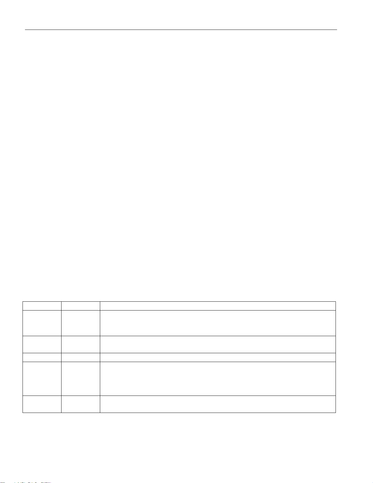
DS2148/Q48
8.2.3 Analog Loopback (ALB)
Setting ALB (CCR6.4) to a one puts the DS2148 in Analog Loop Back. Signals at TTIP and TRING will
be internally connected to RTIP and RRING. The incoming signals at RTIP and RRING will be ignored.
The signals at TTIP and TRING will be transmitted as normal. (See Figure 3-1.)
8.2.4 Dual Loopback (DLB)
Setting both CCR6.7 and CCR6.6 to a one, LLB and RLB respectively, puts the DS2148 into dual
loopback operation. The TCLK and TPOS/TNEG signals will be looped back through the jitter
attenuator (if enabled) and output at RCLK and RPOS/RNEG. Clock and data recovered from RTIP and
RRING will be looped back to the transmit-side and output at TTIP and TRING. This mode of operation
is not available when implementing hardware operation. (See Figure 3-1.)
8.3 PRBS Generation and Detection
Setting TPRBSE (CCR3.4) = 1 enables the DS2148 to transmit a 215-1 (E1) or a 220-1 (T1) Pseudo
Random Bit Sequence (PRBS) depending on the ETS bit setting in CCR1.7. The receive-side of the
DS2148 will always search for these PRBS patterns independent of CCR3.4. The PRBS Bit Error Output
(PBEO) will remain high until the receiver has synchronized to one of the two patterns (64 bits received
without an error) at which time PBEO will go low and the PRBSD bit in the status register (SR) will be
set. Once synchronized, any bit errors received will cause a positive going pulse at PBEO, synchronous
with RCLK. This output can be used with external circuitry to keep track of bit error rates during the
PRBS testing. Setting CCR6.0 (ECRS) = 1 will allow the PRBS errors to be accumulated in the 16-bit
counter in registers ECR1 and ECR2. The PRBS synchronizer will remain in sync until it experiences 6
bit errors or more within a 64 bit span. Both PRBS patterns comply with the ITU-T O.151 specifications.
8.4 Error Counter
Error Count Register 1 (ECR1) is the most significant word and ECR2 is the least significant word of a
user-selectable 16-bit counter that records incoming errors including BiPolar Violations (BPV), Code
Violations (CV), Excessive Zero violations (EXZ) and/or PRBS Errors. See Table 8-3 and Table 8-4 and
Figure 3-2 for details.
DEFINITION OF RECEIVED ERRORS Table 8-3
ERROR E1 OR T1 DEFINITION OF RECEIVED ERRORS
BPV E1/T1 Two consecutive marks with the same polarity. Will ignore BPVs due to
HDB3 and B8ZS zero suppression when CCR2.3 = 0. Typically used with
AMI coding (CCR2.3 = 1). ITU-T O.161.
CV E1 When HDB3 is enabled (CCR2.3 = 0) and the receiver detects two
consecutive BPVs with the same polarity. ITU-T O.161.
EXZ E1 When four or more consecutive zeros are detected.
EXZ T1 When receiving AMI coded signals (CCR2.3 = 1), detection of 16 or more
zeros or a BPV. ANSI T1.403 1999.
When receiving B8ZS coded signals (CCR2.3 = 0), detection of 8 or more
zeros or a BPV. ANSI T1.403 1999.
PRBS E1/T1 A bit error in a received PRBS pattern. See Section 8.3 for details.
ITU-T O.151.
45 of 75
Page 46
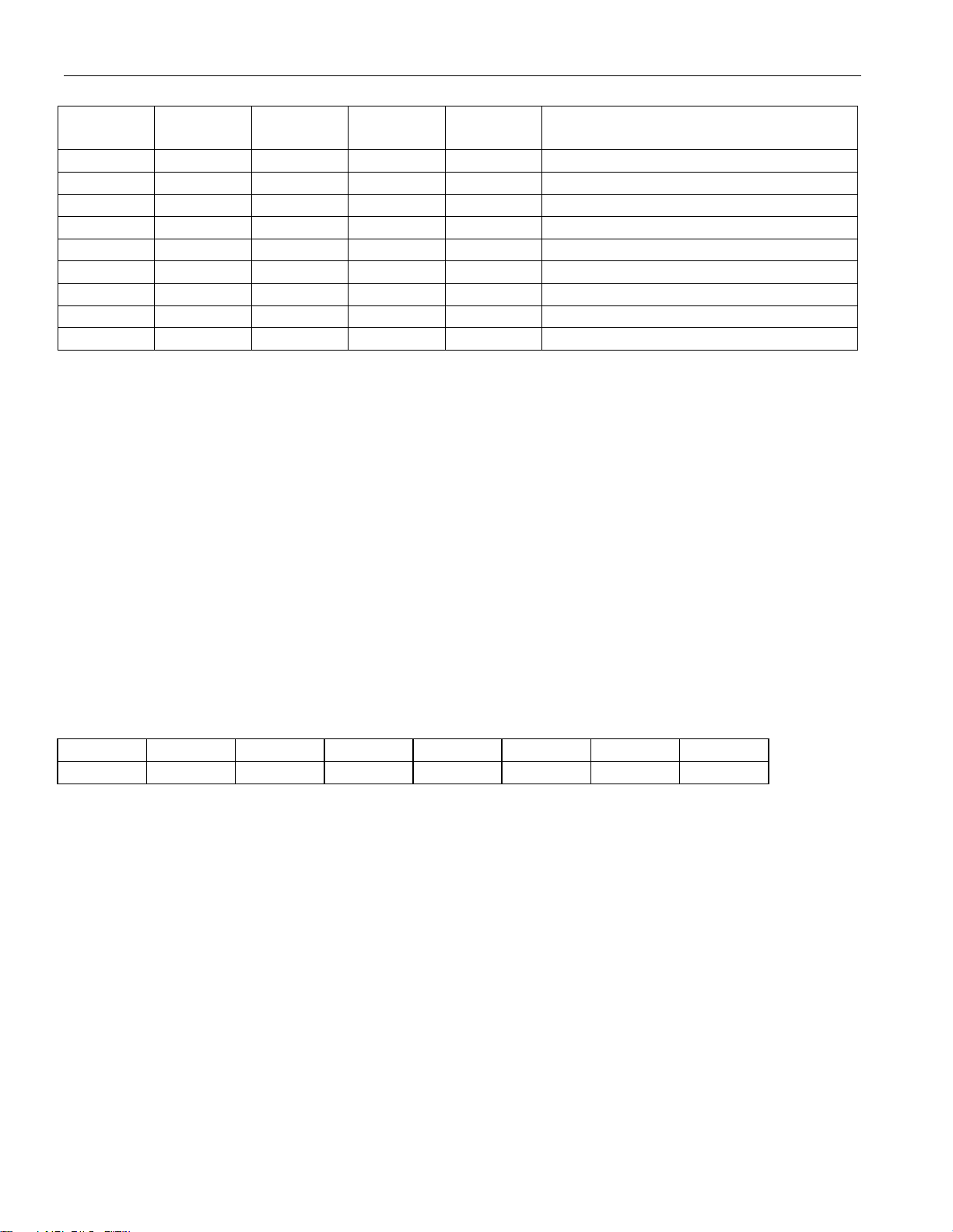
DS2148/Q48
FUNCTION OF ECRS BITS AND RNEG PIN Table 8-4
E1 or T1
(CCR1.7)
0 0 0 0 X CVs
0 0 0 1 X BPVs (HDB3 code words not counted)
0 0 1 0 X CVs + EXZs
0 0 1 1 X BPVs + EXZs
1 0 X 0 0 BPVs (B8ZS code words not counted)
1 0 X 1 0 BPVs + 8 EXZs
1 0 X 0 1 BPVs
1 0 X 1 1 BPVs + 16 EXZs
X 1 X X X PRBS Errors
ECRS2
(CCR6.2)
ECRS1
(CCR6.1)
ECRS0
(CCR6.0)
RHBE
(CCR2.3)
FUNCTION OF ECR
COUNTERS/RNEG1
2
NOTES:
1) RNEG outputs error data only when in NRZ mode (CCR1.6 = 1).
2) PRBS errors will always be output at PBEO independent of ECR control bits and NRZ mode and will
not be present at RNEG.
8.4.1 Error Counter Update
A transition of the ECUE (CCR1.4) control bit from 0 to 1 will update the ECR registers with the current
values and reset the counters. ECUE must be set back to zero and another 0 to 1 transition must occur for
subsequent reads/resets of the ECR registers. Note that the DS2148 can report errors at RNEG when in
NRZ mode (CCR1.6 = 1) by outputting a pulse for each error occurrence. The counter saturates at 65,535
and will not rollover.
ECR1 (11H): UPPER ERROR COUNT REGISTER 1
ECR2 (12H): LOWER ERROR COUNT REGISTER 2
(MSB)
E15 E14 E13 E12 E11 E10 E9 E8 ECR1
E7 E6 E5 E4 E3 E2 E1 E0 ECR2
SYMBOL POSITION DESCRIPTION
E15 ECR1.7
E0 ECR2.0
MSB of the 16-bit error count
LSB of the 16-bit error count
(LSB)
8.5 Error Insertion
When IBPV (CCR3.1) is transitioned from a zero to a one, the device waits for the next occurrence of
three consecutive ones to insert a BPV. IBPV must be cleared and set again for another BPV error
insertion. See figure 3-3 for details on the insertion of the BPV into the datastream.
When IBE (CCR3.0) is transitioned from a zero to a one, the device will insert a logic error. IBE must be
cleared and set again for another logic error insertion. See figure 3-3 for details on the insertion of the
logic error into the datastream.
46 of 75
Page 47

DS2148/Q48
9. ANALOG INTERFACE
9.1 Receiver
The DS2148 contains a digital clock recovery system. The DS2148 couples to the receive E1 or T1
twisted pair (or coaxial cable in 75Ω E1 applications) via a 1:1 transformer. See Table 9-3 or transformer
details. Figure 9-1, Figure 9-2, and Figure 9-3 along with Table 9-1 and Table
termination requirements. The DS2148 has the option of using internal termination resistors.
The DS2148 is designed to be fully software-selectable for E1 and T1 without the need to change any
external resistors for the receive-side. The receive-side will allow the user to configure the DS2148 for
75Ω, 100Ω, or 120Ω receive termination by setting the RT1 (CCR5.1) and RT0 (CCR5.0) bits. When
using the internal termination feature, the Rr resistors should be 60Ω each (Figure 9-1). If external
termination is required, RT1 and RT0 should be set to 0 and both Rr resistors in Figure 9-1 will need to
be 37.5Ω, 50Ω, or 60Ω each depending on the line impedance.
The resultant E1 or T1 clock derived from the 2.048/1.544 PLL (JACLK in Figure 3-1) is internally
multiplied by 16 via another internal PLL and fed to the clock recovery system. The clock recovery
system uses the clock from the PLL circuit to form a 16 times oversampler, which is used to recover the
clock and data. This oversampling technique offers outstanding performance to meet jitter tolerance
specifications shown in Figure 9-6.
Normally, the clock that is output at the RCLK pin is the recovered clock from the E1 AMI/HDB3 or T1
AMI/B8ZS waveform presented at the RTIP and RRING inputs. When no signal is present at RTIP and
RRING, a Receive Carrier Loss (RCL) condition will occur and the RCLK will be derived from the
JACLK source (Figure 3-1). If the jitter attenuator is placed in the receive path (as is the case in most
applications), the jitter attenuator restores the RCLK to an approximate 50% duty cycle. If the jitter
attenuator is either placed in the transmit path or is disabled, the RCLK output can exhibit slightly shorter
high cycles of the clock. This is due to the highly oversampled digital clock recovery circuitry. See the
Receive AC Timing Characteristics in Section 12 for more details.
The receive-side circuitry also contains a clock synthesizer which outputs a user configurable clock (up to
16.384MHz) synthesized to RCLK at BPCLK (pin 31). See Table 6-3 for details on output clock
frequencies at BPCLK. In hardware mode, BPCLK defaults to a 16.384MHz output.
The DS2148 has a bypass mode for the receive side clock and data. This allows the BPCLK to be
derived from RCLK after the jitter attenuator while the clock and data presented at RCLK, RPOS, and
RNEG go unaltered. This is intended for applications where the receive side jitter attenuation will be
done after the LIU. Setting RJAB (CCR6.3) to a logic 1 will enable the bypass. Be sure that the jitter
attenuator is in the receive path (CCR4.3 = 0). See Figure 3-1 for details.
The DS2148 will report the signal strength at RTIP and RRING in 2.5dB increments via RL3-RL0
located in the Receive Information Register 2. This feature is helpful when trouble shooting line
performance problems. See Table 7-2 for details.
Monitor applications in both E1 and T1 require various flat gain settings for the receive-side circuitry.
The DS2148 can be programmed to support these applications via the Monitor Mode control bits MM1
and MM0. When the monitor modes are enabled, the receiver will tolerate normal line loss up to –6dB.
See Table 6-4 for details.
9-2 show the receive
47 of 75
Page 48

DS2148/Q48
9.2 Transmitter
The DS2148 uses a set of laser-trimmed delay lines along with a precision digital-to-analog converter
(DAC) to create the waveforms that are transmitted onto the E1 or T1 line. The waveforms created by
the DS2148 meet the latest ETSI, ITU, ANSI, and AT&T specifications. The user will select which
waveform is to be generated by setting the ETS bit (CCR1.7) for E1 or T1 operation, then programming
the L2/L1/L0 bits in Common Control Register 4 for the appropriate application. See Table 9-1 and
Table 9-2 for the proper L2/L1/L0 settings.
A 2.048MHz or 1.544MHz TTL clock is required at TCLK for transmitting data at TPOS and TNEG.
ITU specification G.703 requires an accuracy of ±50ppm for both T1 and E1. TR62411 and ANSI specs
require an accuracy of ±32ppm for T1 interfaces. The clock can be sourced internally by RCLK or
JACLK. See CCR1.2, CCR1.1, CCR1.0, and Figure 3.3 for details. Because of the nature of the DS2148
transmitter design, very little jitter (less than 0.005 UIpp broadband from 10Hz to 100kHz) is added to the
jitter present on TCLK. Also, the waveforms created are independent of the duty cycle of TCLK. The
transmitter in the DS2148 couples to the E1 or T1 transmit twisted pair (or coaxial cable in some E1
applications) via a 1:1.36 step-up transformer. In order for the device to create the proper waveforms, the
transformer used must meet the specifications listed in Table 9-3.
The DS2148 has automatic short-circuit limiter that limits the source current to 50mA (rms) into a 1Ω
load. This feature can be disabled by setting the SCLD bit (CCR2.5) = 1. When the current limiter is
activated, TCLE (SR.2) will be set even if short circuit limiter is disabled. The TPD bit (CCR4.0) will
power-down the transmit line driver and 3-state the TTIP and TRING pins. The DS2148 also can detect
when the TTIP or TRING outputs are open-circuited. When an open circuit is detected, TOCD (SR.1)
will be set.
9.3 Jitter Attenuator
The DS2148 contains an onboard jitter attenuator that can be set to a depth of either 32 bits or 128 bits via
the JABDS bit (CCR4.2). In hardware mode the depth is 128 bits and cannot be changed. The 128-bit
mode is used in applications where large excursions of wander are expected. The 32-bit mode is used in
delay sensitive applications. The characteristics of the attenuation are shown in figure 9-7. The jitter
attenuator can be placed in either the receive path or the transmit path by appropriately setting or clearing
the JAS bit (CCR4.3). Also, the jitter attenuator can be disabled (in effect, removed) by setting the DJA
bit (CCR4.1). In order for the jitter attenuator to operate properly, a 2.048MHz or 1.544MHz clock must
be applied at MCLK. ITU specification G.703 requires an accuracy of ±50ppm for both T1 and E1.
TR62411 and ANSI specs require an accuracy of ±32ppm for T1 interfaces. There is an onboard PLL for
the jitter attenuator, which will convert the 2.048MHz clock to a 1.544MHz rate for T1 applications.
Setting JAMUX (CCR1.3) to a logic 0 bypasses this PLL. Onboard circuitry adjusts either the recovered
clock from the clock/data recovery block or the clock applied at the TCLK pin to create a smooth jitter
free clock which is used to clock data out of the jitter attenuator FIFO. It is acceptable to provide a
gapped/bursty clock at the TCLK pin if the jitter attenuator is placed on the transmit side. If the incoming
jitter exceeds either 120 UIpp (buffer depth is 128 bits) or 28 UIpp (buffer depth is 32 bits), then the
DS2148 will divide the internal nominal 32.768MHz (E1) or 24.704MHz (T1) clock by either 15 or 17
instead of the normal 16 to keep the buffer from overflowing. When the device divides by either 15 or 17,
it also sets the jitter attenuator limit trip (JALT) bit in the receive information register 1 (RIR1).
48 of 75
Page 49
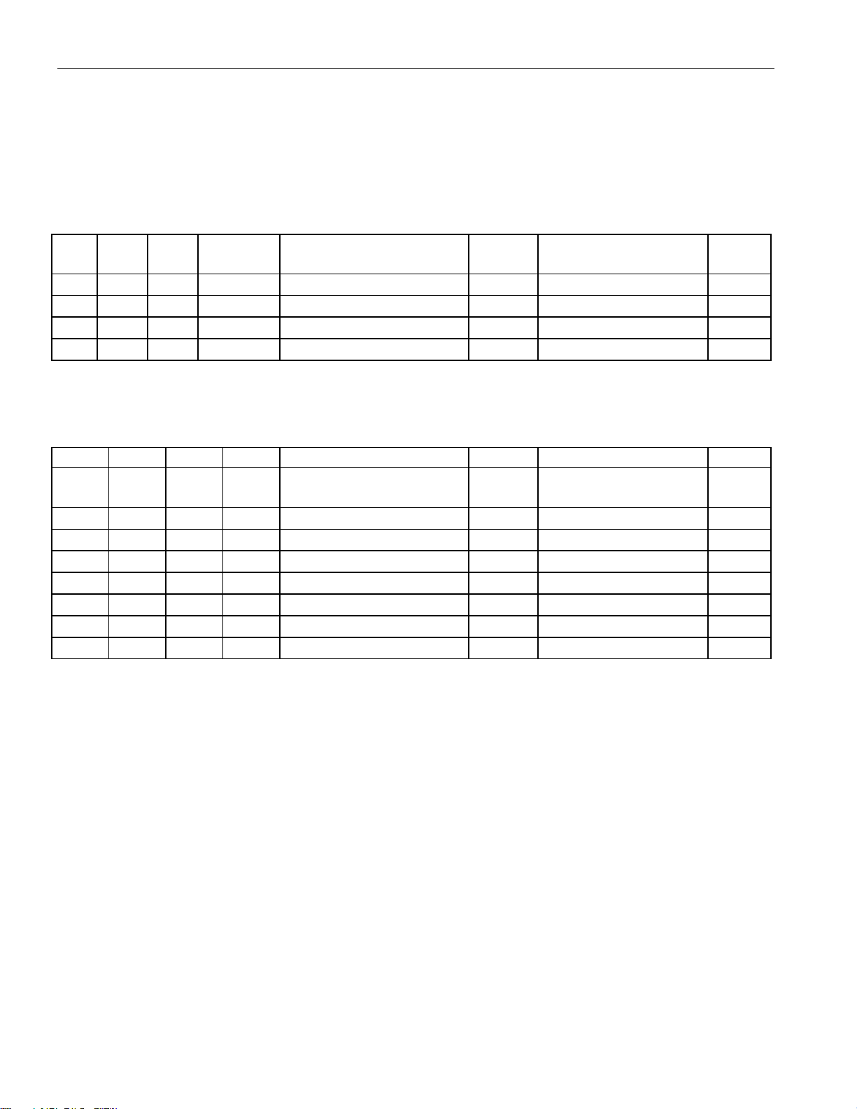
DS2148/Q48
9.4 G.703 Synchronization Signal
The DS2148 is capable of receiving a 2.048MHz square-wave synchronization clock as specified in
section 13 of ITU G.703 (10/98). To use the DS2148 in this mode, set the receive synchronization clock
enable (CCR5.3) = 1. The DS2148 can also transmit the 2.048MHz square-wave synchronization clock as
specified in Section 10 of G.703. To transmit the 2.048MHz clock, set the transmit synchronization clock
enable (CCR5.2) = 1.
LINE BUILD OUT SELECT FOR E1 IN REGISTER CCR4 (ETS = 0) Table 9-1
L2 L1 L0 VDD APPLICATION N RETURN LOSS Rt
0 0 0 5V
0 0 1 5V
1 0 0 5V
1 0 1 5V
75W normal
120W normal
75W w/ high return loss
120W w/ high return loss
1:1.36 NM
1:1.36 NM
1:1.36 21 dB
1:1.36 21 dB
0W
0W
18W
27W
Note: See Figure 9-1, Figure 9-2, and Figure 9-3.
LINE BUILD OUT SELECT FOR T1 IN REGISTER CCR4 (ETS = 1) Table 9-2
L2 L1 L0 VDD APPLICATION N RETURN LOSS Rt
0 0 0 5V DSX-1 (0 to 133 feet) /
0 DB CSU
0 0 1 5V DSX-1 (133 to 266 feet) 1:1.36 NM
0 1 0 5V DSX-1 (266 to 399 feet) 1:1.36 NM
0 1 1 5V DSX-1 (399 to 533 feet) 1:1.36 NM
1 0 0 5V DSX-1 (533 to 655 feet) 1:1.36 NM
1 0 1 5V -7.5dB CSU 1:1.36 NM
1 1 0 5V -15dB CSU 1:1.36 NM
1 1 1 5V -22.5dB CSU 1:1.36 NM
Note: See Figure 9-1, Figure 9-2, and Figure 9-3.
1:1.36 NM
0W
0W
0W
0W
0W
0W
0W
0W
49 of 75
Page 50
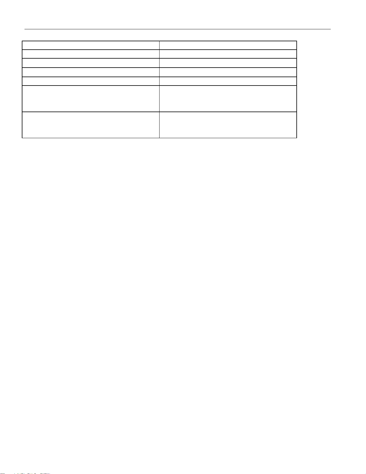
TRANSFORMER SPECIFICATIONS FOR 5V OPERATION Table 9-3
SPECIFICATION RECOMMENDED VALUE
Turns Ratio 5V Applications 1:1(receive) and 1:1.36(transmit) ±2%
Primary Inductance
Leakage Inductance
Interwinding Capacitance 40pF maximum
Transmit Transformer DC Resistance
Primary (Device Side)
Secondary
Receive Transformer DC Resistance
Primary (Device Side)
Secondary
600mH minimum
1.0mH maximum
1.2W maximum
1.2W maximum
1.2W maximum
1.2W maximum
DS2148/Q48
50 of 75
Page 51
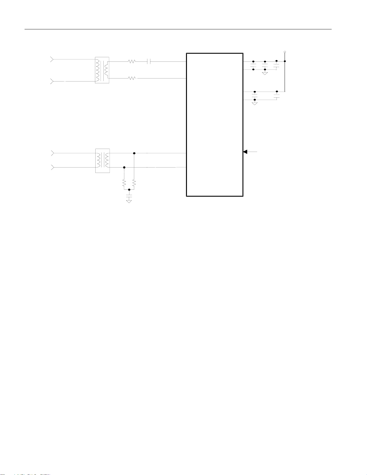
DS2148/Q48
rRrRt
t
BASIC INTERFACE Figure 9-1
Transmi
Line
Receive
Line
N:1
(larger winding
toward the network)
1:1
R
0.1µF
Rt
0.47µF
(non
polarized)
TTIP
TRING
RTIP
RRING
DS2148
VDD(21)
V
SS
VDD (36)
V
SS
MCLK
(22)
(35)
0.1µF
0.01µF
0.1µF
2.048MHz
(this clock can also
be 1.544MHz for T1
only applications)
10µF
10µF
+V
DD
NOTES:
1) All resistor values are ±1%.
2) In E1 applications, the Rt resistors are used to increase the transmitter return loss (Table 9-1). No
return loss is required for T1 applications.
3) The Rr resistors should be set to 60W each if the internal receive-side termination feature is enabled.
When this feature is disabled, Rr = 37.5W for 75W, 60W for 120W E1 systems, or 50W for 100W
T1 lines.
4) See Table 9-1 and Table 9-2 for the appropriate transmit transformer turns ratio (N).
51 of 75
Page 52
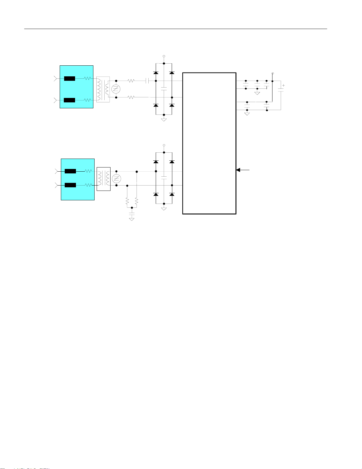
DS2148/Q48
-
t
PROTECTED INTERFACE USING INTERNAL RECEIVE TERMINATION
Figure 9-2
Transmi
Line
Receive
Line
(optional)
Fuse
Fuse
Fuse
Fuse
(optional)
Rp
Rp
N:1
(larger winding
toward the network)
Rp
Rp
1:1
Rt
S
polarized)
Rt
S
60 60
0.1uF
D1
0.47uF
(non
D3 D4
D5
D7
+VDD
C1
+VDD
C2
D6
D8
D2
TTIP
TRING
RTIP
RRING
DS2148
VDD (21)
VSS (22)
VDD (36)
VSS (35)
MCLK
0.1uF
0.01uF
10uF
0.1uF
10uF
2.048MHz
(this clock can also
be 1.544MHz for T1
only applications)
+VDD
68uF
NOTES:
1) All resistor values are ±1%.
2) C1 = C2 = 0.1µF.
3) S is a 6V transient suppresser.
4) D1 to D8 are Schottky diodes.
5) The fuses are optional to prevent AC power line crosses from compromising the transformers.
6) Rp resistors exist to keep the Fuses from opening during a surge. If they are used, then the 60W
receive termination resistance must be adjusted to match the line impedance.
7) The Rt resistors are used to increase the transmitter return loss (Table 9-1). No return loss is required
for T1 applications.
8) The transmit transformer turns ratio (N) would be 1:1.36 for 5V operation.
9) The 68mF is used to keep the local power plane potential within tolerance during a surge.
52 of 75
Page 53
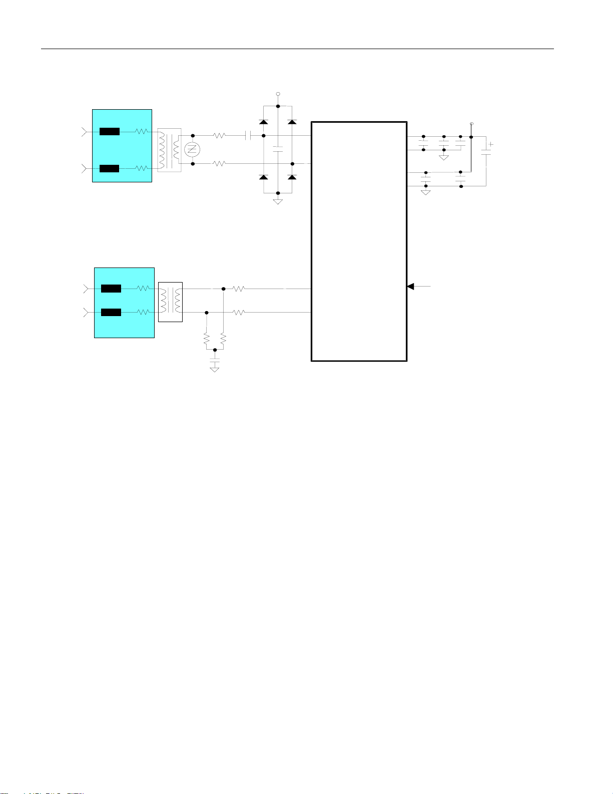
DS2148/Q48
rRr
t
PROTECTED INTERFACE USING EXTERNAL RECEIVE TERMINATION
Figure 9-3
Transmi
Line
Receive
Line
(optional)
Fuse
Fuse
Fuse
Fuse
(optional)
Rp
Rp
N:1
(larger winding
toward the network)
Rp
Rp
1:1
R
0.1µF
D1
Rt
Rt
0.47µF
(non-
polarized)
D3 D4
470
470
S
C1
+V
DD
D2
TTIP
TRING
RTIP
RRING
DS2148
VDD(21)
V
SS
V
DD
V
SS
MCLK
(22)
(36)
(35)
0.1µF
0.01µF
10µF
0.1µF
10µF
2.048MHz
(this clock can also
be 1.544MHz for T1
only applications)
+V
DD
68µF
NOTES:
1) All resistor values are ±1%.
2) C1 = 0.1µF.
3) S is a 6V transient suppresser.
4) D1 to D4 are Schottky diodes.
5) The fuses are optional to prevent AC power line crosses from compromising the transformers.
6) Rp resistors exist to keep the Fuses from opening during a surge. If they are used, then Rr must be
adjusted to match the line impedance.
7) Rr = 37.5W for 75W, 60W for 120W E1 systems, or 50W for 100W T1 lines.
8) The Rt resistors are used to increase the transmitter return loss (Table 9-1). No return loss is required
for T1 applications.
9) The transmit transformer turns ratio (N) would be 1:1.36 for 5V operation.
10) The 68mF is used to keep the local power plane potential within tolerance during a surge.
53 of 75
Page 54
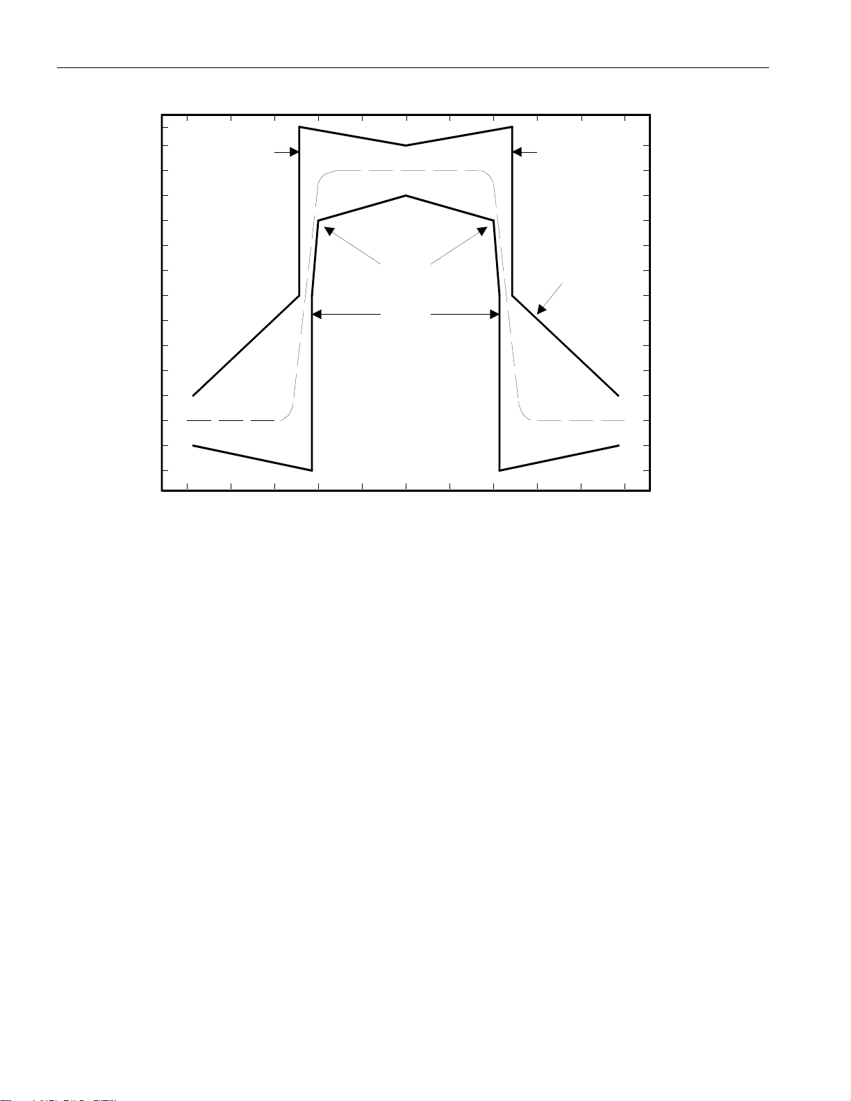
E1 TRANSMIT PULSE TEMPLATE Figure 9-4
1.2
DS2148/Q48
SCALED AMPLITUDE
1.1
1.0
0.9
0.8
0.7
0.6
0.5
0.4
0.3
0.2
0.1
0
(in 75 ohm systems, 1.0 on the scale = 2.37Vpeak
in 120 ohm systems, 1.0 on the scale = 3.00Vpeak)
-0.1
-0.2
194ns
219ns
0
TIME (ns)
50 100 150 200 250-50-100-150-200-250
269ns
G.703
Template
54 of 75
Page 55
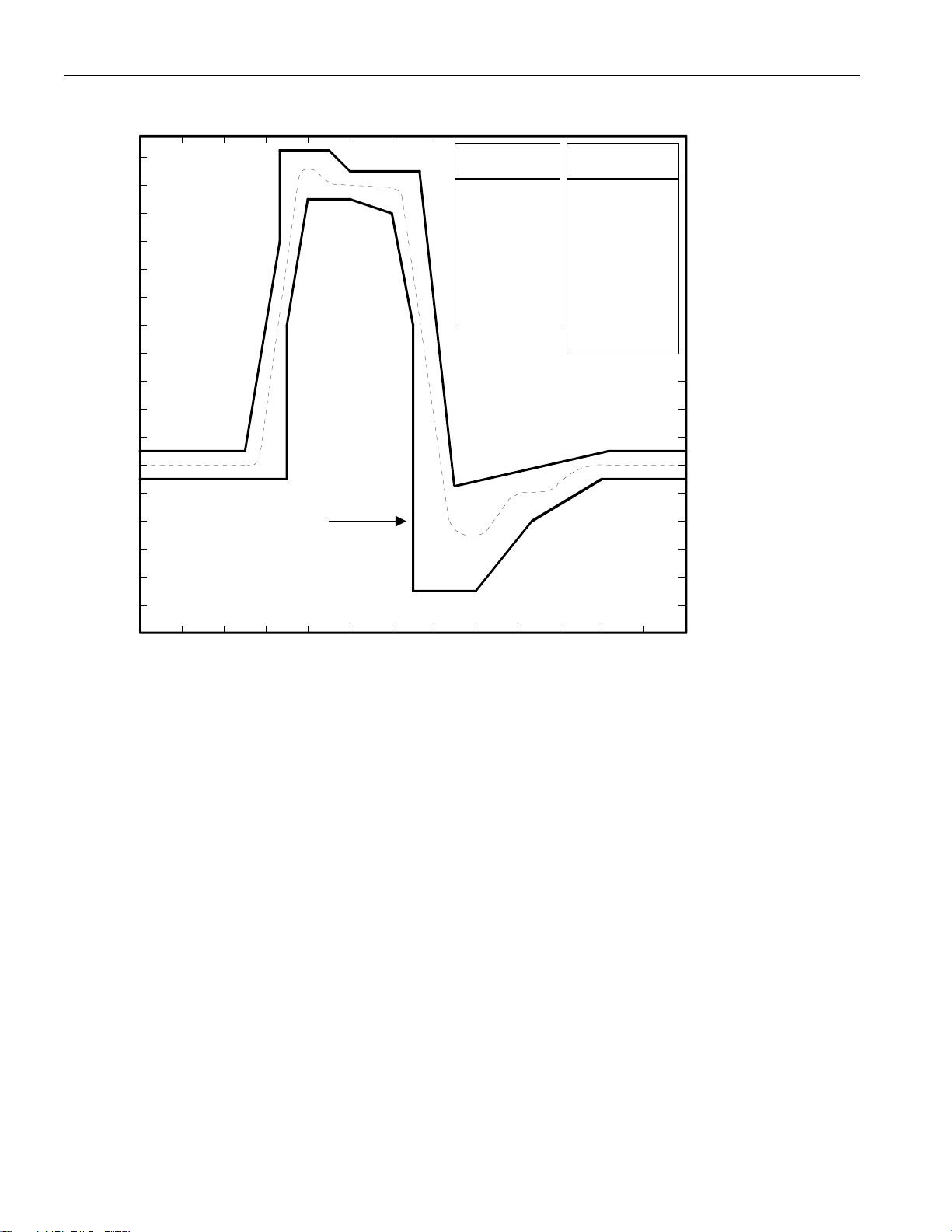
T1 TRANSMIT PULSE TEMPLATE Figure 9-5
1.2
1.1
1.0
0.9
0.8
0.7
0.6
0.5
0.4
0.3
0.2
0.1
NORMALIZED AMPLITUDE
-0.1
-0.2
-0.3
0
T1.102/87, T1.403,
CB 119 (Oct. 79), &
I.431 Template
MAXIMUM CURVE
UI Time Amp.
-500
-0.77
-255
-0.39
-175
-0.27
-175
-0.27
-75
-0.12
0
0.00
175
0.27
225
0.35
600
0.93
750
1.16
0.05
0.05
0.80
1.15
1.15
1.05
1.05
-0.07
0.05
0.05
MINIMUM CURVE
UI Time Amp.
-0.05
-500
-0.77
-0.23
-0.23
-0.15
0.00
0.15
0.23
0.23
0.46
0.66
0.93
1.16
-150
-150
-100
0
100
150
150
300
430
600
750
-0.05
0.50
0.95
0.95
0.90
0.50
-0.45
-0.45
-0.20
-0.05
-0.05
DS2148/Q48
-0.4
-0.5
-400 -200 200 400 600100
-500 -300 -100 0 300 500 700
TIME (ns)
55 of 75
Page 56
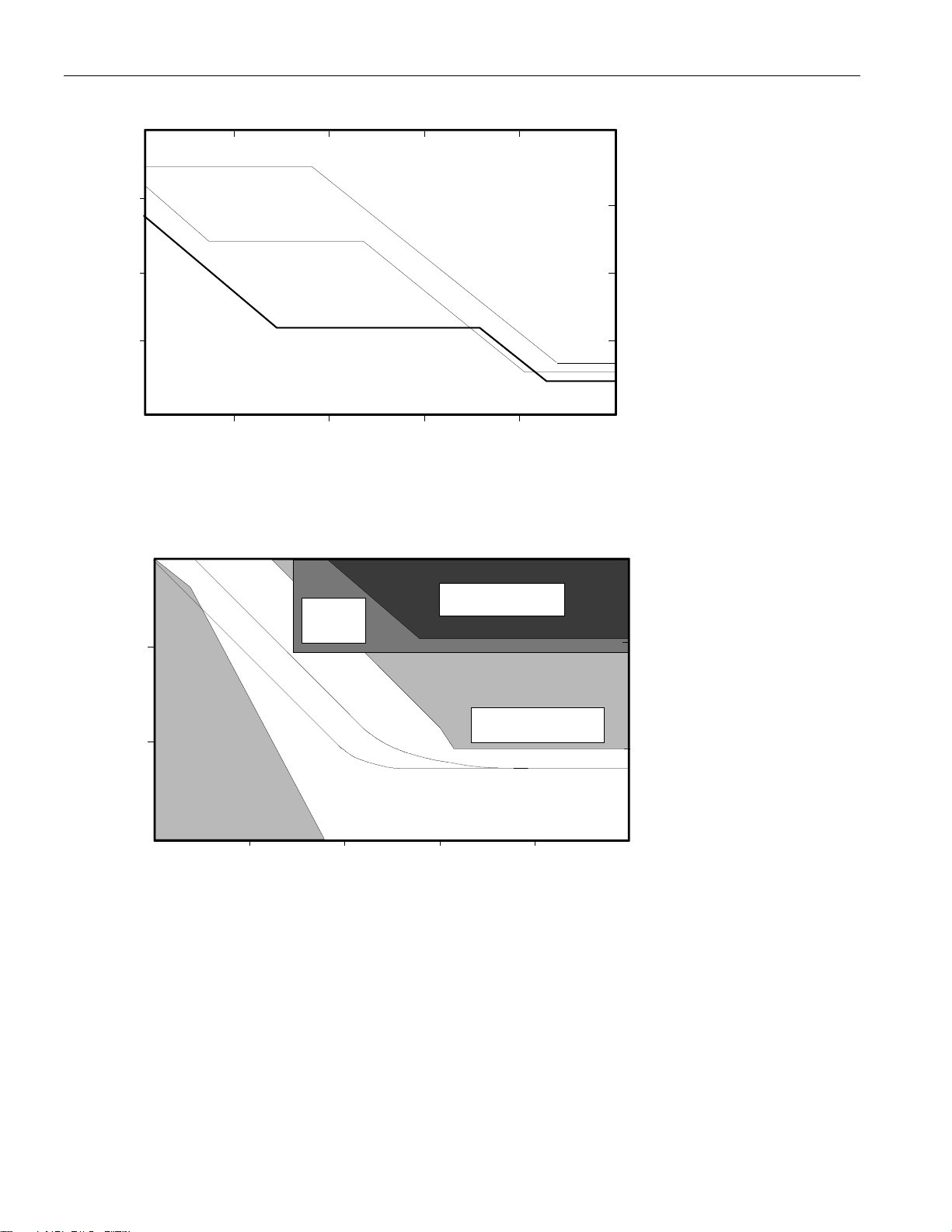
JITTER TOLERANCE Figure 9-6
1K
DS2148/Q48
100
TR 62411 (Dec. 90)
10
ITU-T G.823
UNIT INTERVALS (UIpp)
1
0.1
1
10 100 1K 10K 100K
FREQUENCY (Hz)
JITTER ATTENUATION Figure 9-7
0dB
TBR12
Prohibited
Area
-20dB
-40dB
JITTER ATTENUATION (dB)
C
u
r
v
e
B
C
ur
ve
A
T1E1
DS2148
Tolerance
ITU G.7XX
Prohibited Area
TR 62411 (Dec. 90)
Prohibited Area
-60dB
1 10 100 1K 10K
FREQUENCY (Hz)
56 of 75
100K
Page 57
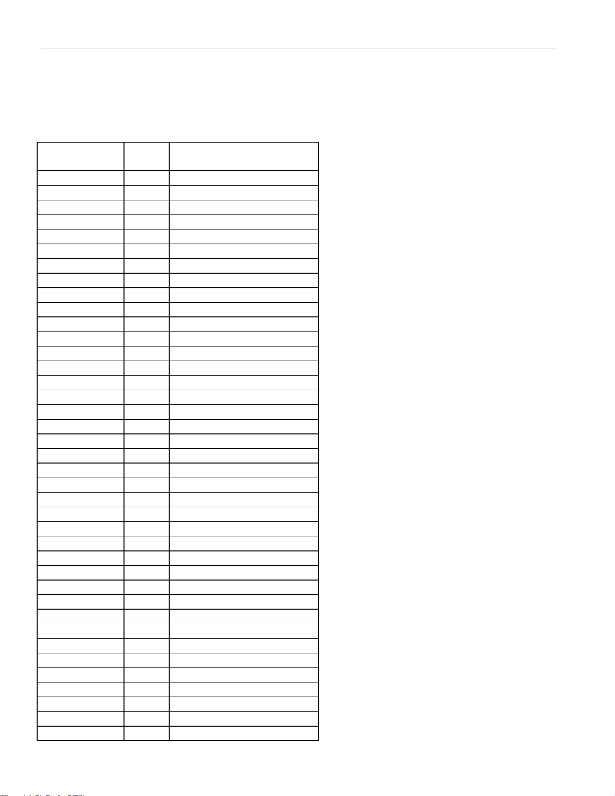
DS2148/Q48
10. DS21Q48 QUAD LIU
The DS21Q48 is a quad version of the DS2148G utilizing CABGA on carrier packaging technology. The
four LIUs are controlled via the parallel port mode. Serial and hardware modes are unavailable in this
package.
DS21Q48 PIN ASSIGNMENT Table 10-1
DS21Q48
PIN#
J1 I Connect to VSS
K3 I Connect to VSS
J2 I RD*(DS*)
H1 I WR*(R/W*)
K2 I ALE(AS)
K1 I/O A4
L1 I A3
H11 I A2
H12 I A1
G12 I A0
J10 I/O D7/AD7
H10 I/O D6/AD6
G11 I/O D5/AD5
J9 I/O D4/AD4
E3 I/O D3/AD3
D4 I/O D2/AD2
F3 I/O D1/AD1
D5 I/O D0/AD0
G4 I VSM
K9 I/O INT*
K7 I TEST
L9 I HRST*
J6 I MCLK
L7 I BIS0
M8 I BIS1
M12 I PBTS
J3 I CS*1
D3 I CS*2
D10 I CS*3
K10 I CS*4
K5 O PBEO1
G3 O PBEO2
E10 O PBEO3
K8 O PBEO4
L6 O RCL/LOTC1
D7 O RCL/LOTC2
F9 O RCL/LOTC3
I/O PARALLEL
PORT MODE
57 of 75
Page 58
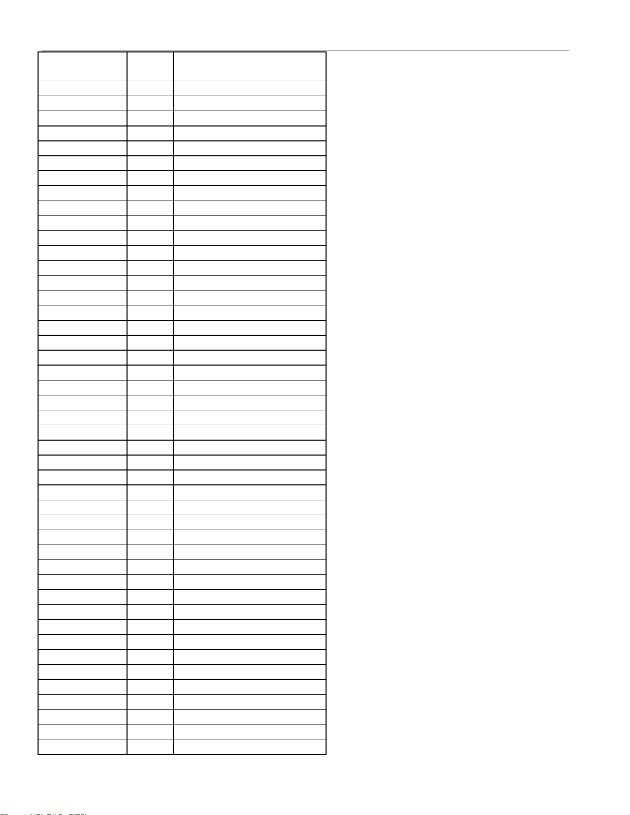
DS21Q48
PIN#
I/O PARALLEL
PORT MODE
J7 O RCL/LOTC4
A1 I RTIP1
A4 I RTIP2
A7 I RTIP3
A10 I RTIP4
B2 I RRING1
B5 I RRING2
B8 I RRING3
B11 I RRING4
H4 O BPCLK1
D6 O BPCLK2
F10 O BPCLK3
L8 O BPCLK4
A2 O TTIP1
A5 O TTIP2
A8 O TTIP3
A11 O TTIP4
B3 O TRING1
B6 O TRING2
B9 O TRING3
B12 O TRING4
K4 O RPOS1
E1 O RPOS2
D11 O RPOS3
K11 O RPOS4
G2 O RNEG1
E2 O RNEG2
F11 O RNEG3
M10 O RNEG4
H3 O RCLK1
F1 O RCLK2
E11 O RCLK3
L11 O RCLK4
G1 I TPOS1
F2 I TPOS2
E12 I TPOS3
M11 I TPOS4
H2 I TNEG1
M1 I TNEG2
D12 I TNEG3
K12 I TNEG4
M2 I TCLK1
L2 I TCLK2
F12 I TCLK3
L12 I TCLK4
DS2148/Q48
58 of 75
Page 59
DS21Q48
I/O PARALLEL
PIN#
J5 - V
D2 - V
G9 - V
M9 - V
L5 - V
E4 - V
D8 - V
J8 - V
J4 - V
D1 - V
E9 - V
L10 - V
M4 - V
F4 - V
D9 - V
H9 - V
PORT MODE
DD1
DD2
DD3
DD4
DD1
DD2
DD3
DD4
SS1
SS2
SS3
SS4
SS1
SS2
SS3
SS4
DS2148/Q48
59 of 75
Page 60
BGA 12 x 12 PIN LAYOUT Figure 10-1
A
B
C
D
E
F
G
H
J
K
L
M
1
RTIP
1
NC RRING
NC
VSS
2
RPOS
2
RCLK
2
TPOS
1
WR*
(R/W*)
See
Note 2
A4
A3 TCLK
TNEG
2
2
TTIP
1
1
NC
VDD
2
RNEG
2
TPOS
2
RNEG
1
TNEG
1
RD*
(DS*)
ALE
(AS)
2
TCLK
1
3
NC RTIP
TRING
1
NC
CS*
2
D3/
AD3
D1/
AD1
PEBO
2
RCLK
CS*
See
Note 2
NC
NC VSS
BPCLK
1
1
RPOS
4
2
NC RRING
NC
D2/
AD2
VDD
2
VSS
2
VSM
1
VSS
1
1
NC VDD
1
5
TTIP
2
2
NC
D0/
AD0
NC
NC
NC
NC
VDD
1
PEBO
1
1
NC
6
NC RTIP
TRING
2
NC
BPCLK
2
NC
NC
NC
NC
MCLK RCL/
NC TEST PEBO
RCL/
LOTC1
NC
NOTES:
1) Shaded areas are signals common to all four devices.
2) Connect to V
SS
.
7
3
NC RRING
NC
RCL/
LOTC2
NC
NC
NC
NC
LOTC4
BIS0 BPCLK
NC BIS1 VDD
8
TTIP
3
TRING
3
NC
VDD
3
NC VSS
NC RCL/
LOTC3
NC VDD
NC VSS
VDD
4
4
HRST* VSS
4
9
NC RTIP
3
NC
VSS
3
3
3
4
D4/
AD4
INT* CS*
4
10
4
NC RRING
NC
CS*
3
PEBO
3
BPCLK
3
NC
D6/
AD6
D7/
AD7
4
4
RNEG
4
DS2148/Q48
11
TTIP
4
4
NC
RPOS
3
RCLK
3
RNEG
3
D5/
AD5
A2
NC
RPOS
4
RCLK
4
TPOS
4
12
NC
TRING
4
NC
TNEG
3
TPOS
3
TCLK
3
A0
A1
NC
TNEG
4
TCLK
4
PBTS
60 of 75
Page 61
DS2148/Q48
11. DC CHARACTERISTICS
ABSOLUTE MAXIMUM RATINGS*
Voltage Range on Any Pin Relative to Ground -1.0V to +6.0V
Operating Temperature Range for DS2148TN
Storage Temperature Range See J-STD-020A specification
* This is a stress rating only and functional operation of the device at these or any other conditions
beyond those indicated in the operation sections of this specification is not implied. Exposure to
absolute maximum rating conditions for extended periods of time can affect reliability.
-40°C to +85°C
RECOMMENDED DC OPERATING CONDITIONS (-40°C to +85°C)
PARAMETER SYMBOL MIN TYP MAX UNITS NOTES
Logic 1 VIH 2.0 5.5 V
Logic 0 VIL –0.3 +0.8 V
Supply for 5V Operation VDD 4.75 5 5.25 V 1
CAPACITANCE
PARAMETER SYMBOL MIN TYP MAX UNITS NOTES
Input Capacitance CIN 5 pF
Output Capacitance C
7 pF
OUT
DC CHARACTERISTICS (-40°C to +85°C; V
PARAMETER SYMBOL MIN TYP MAX UNITS NOTES
Input Leakage IIL –1.0 +1.0
Output Leakage ILO 1.0
Output Current (2.4V) IOH –1.0 mA
Output Current (0.4V) IOL +4.0 mA
Supply Current IDD - 95 125 MA 2, 5
(T
= +25°C)
A
= 5.0V ± 5%)
DD
mA
mA
3
4
NOTES:
1) Applies to VDD.
2) TCLK = MCLK = 2.048MHz.
3) 0.0V < VIN < VDD.
4) Applied to INT* when 3-stated.
5) Power dissipation with TTIP and TRING driving a 30W load, for an all one’s data density.
61 of 75
Page 62
DS2148/Q48
THERMAL CHARACTERISTICS OF DS21Q48 BGA PACKAGE
PARAMETER MIN TYP MAX NOTES
Ambient Temperature -40ºC - +85ºC 1
Junction Temperature - - +125ºC
Theta-JA (θJA) in Still Air - +24ºC/W - 2
Theta-JC (θJC) in Still Air - +4.1ºC/W - 3
NOTES:
1) The package is mounted on a four-layer JEDEC-standard test board.
2) Theta-JA (θJA) is the junction to ambient thermal resistance, when the package is mounted on a fourlayer JEDEC-standard test board.
3) While Theta-JC (θJC) is commonly used as the thermal parameter that provides a correlation between the
junction temperature (Tj) and the average temperature on top center of four of the chip-scale BGA
packages (TC), the proper term is Psi-JT. It is defined by:
(TJ - TC) / overall package power
The method of measurement of the thermal parameters is defined in EIA/JEDEC-standard document
EIA-JESD51-2.
THETA-JA (θJA) VERSUS AIRFLOW
FORCED AIR (m/s)
0 24ºC/W
1 21ºC/W
2.5 19ºC/W
THETA-JA (θJA)
62 of 75
Page 63

12. AC CHARACTERISTICS
AC CHARACTERISTICS—MULTIPLEXED PARALLEL PORT
DS2148/Q48
(BIS1 = 0, BIS0 = 0) (-40°C to +85°C; V
= 5.0V ± 5%)
DD
PARAMETER SYMBOL MIN TYP MAX UNITS NOTES
Cycle Time t
Pulse Width, DS Low or RD*
200 ns
CYC
PWEL 100 ns
High
Pulse Width, DS High or RD*
PWEH 100 ns
Low
Input Rise/Fall times tR, tF 20 ns
R/W* Hold Time t
R/W* Setup Time Before DS
10 ns
RWH
t
50 ns
RWS
High
CS* Setup Time Before DS,
tCS 20 ns
WR* or RD* Active
CS* Hold Time tCH 0 ns
Read Data Hold Time t
Write Data Hold Time t
Muxed Address Valid to AS
10 50 ns
DHR
0 ns
DHW
t
15 ns
ASL
or ALE Fall
Muxed Address Hold Time t
Delay Time DS, WR* or RD*
10 ns
AHL
t
20 ns
ASD
to AS or ALE Rise
Pulse Width AS or ALE High PW
Delay Time, AS or ALE to
30 ns
ASH
t
10 ns
ASED
DS, WR* or RD*
Output Data Delay Time
t
20 80 ns
DDR
From DS or RD*
Data Setup Time t
50 ns
DSW
See Figure 12-1, Figure 12-2, Figure 12-3
63 of 75
Page 64
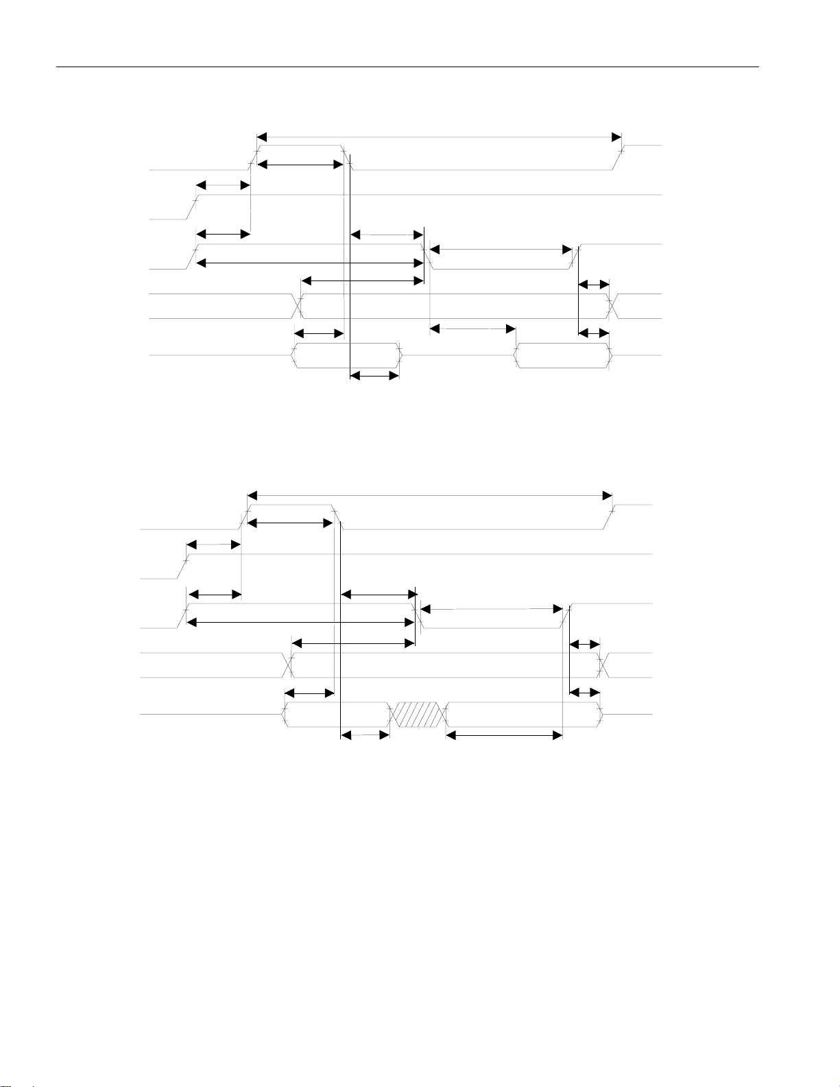
INTEL BUS READ TIMING (PBTS = 0, BIS1 = 0, BIS0 = 0) Figure 12-1
t
CYC
ALE
PW
t
ASD
EL
ASH
t
t
CS
ASED
PW
EH
t
CH
WR*
RD*
CS*
t
ASD
PW
DS2148/Q48
AD0-AD7
t
ASL
t
AHL
t
DDR
t
DHR
INTEL BUS WRITE TIMING (PBTS = 0, BIS1 = 0, BIS0 = 0) Figure 12-2
t
CYC
ALE
PW
EL
t
ASL
ASH
t
ASED
t
CS
PW
EH
t
CH
t
DHW
RD*
WR*
CS*
AD0-AD7
t
ASD
t
ASD
PW
t
AHL
64 of 75
t
DSW
Page 65
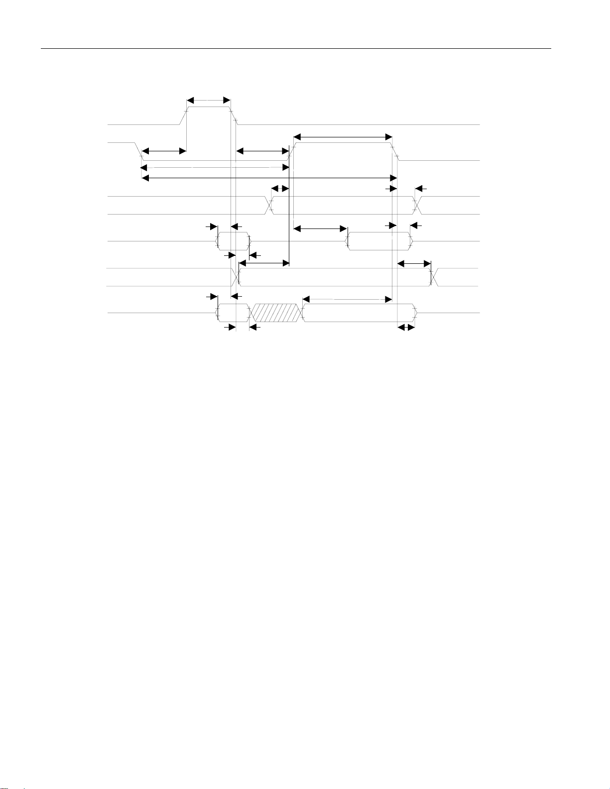
MOTOROLA BUS TIMING (PBTS = 1, BIS1 = 0, BIS0 = 0) Figure 12-3
PW
ASH
AS
PW
t
EH
CH
t
t
DHR
t
DHW
RWH
DS
R/W*
AD0-AD7
(read)
CS*
AD0-AD7
(write)
PW
EL
t
ASD
t
ASL
t
ASL
t
t
AHL
AHL
t
ASED
t
RWS
t
CS
t
DDR
t
CYC
t
DSW
DS2148/Q48
65 of 75
Page 66

AC CHARACTERISTICS—NONMULTIPLEXED PARALLEL PORT
DS2148/Q48
(BIS1 = 0, BIS0 = 1) (-40°C to +85°C; V
PARAMETER SYMBOL MIN TYP MAX UNITS NOTES
Setup Time for A0 to A4, Valid
to CS* Active
Setup Time for CS* Active to
Either RD*, WR*, or DS*
Active
Delay Time From Either RD*
or DS* Active to Data Valid
Hold Time From Either RD*,
WR*, or DS* Inactive to CS*
Inactive
Hold Time From CS* Inactive
to Data Bus 3-State
Wait Time From Either WR* or
DS* Active to Latch Data
Data Setup Time To Either
WR* or DS* Inactive
Data Hold Time From Either
WR* or DS* Inactive
Address Hold From Either WR*
or DS* Inactive
See Figure 12-4, Figure 12-5, Figure 12-6, and Figure 12-7
t1 0 ns
t2 0 ns
t3 75 ns
t4 0 ns
t5 5 20 ns
t6 75 ns
t7 10 ns
t8 10 ns
t9 10 ns
= 5.0V ± 5%)
DD
66 of 75
Page 67
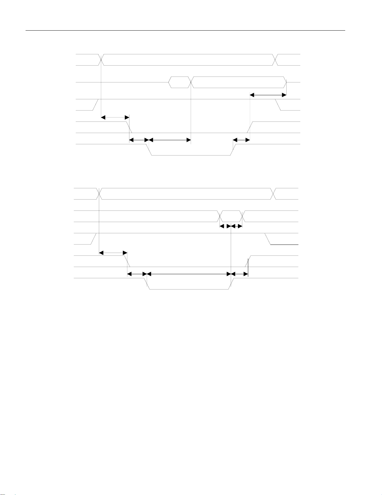
INTEL BUS READ TIMING (PBTS = 0, BIS1 = 0, BIS0 = 1) Figure12-4
DS2148/Q48
A0 to A4
D0 to D7
WR*
t1
CS*
0ns min.
RD*
Address Valid
Data Valid
5ns min. / 20ns max.
0ns min.
t2 t3 t4
75ns max.
t5
0ns min.
INTEL BUS WRITE TIMING (PBTS = 0, BIS1 = 0, BIS0 = 1) Figure 12-5
Address ValidA0 to A4
D0 to D7
t7 t8
RD*
CS*
WR*
t1
0ns min.
0ns min.
t2 t6 t4
75ns min.
10ns
min.
10ns
min.
0ns min.
67 of 75
Page 68
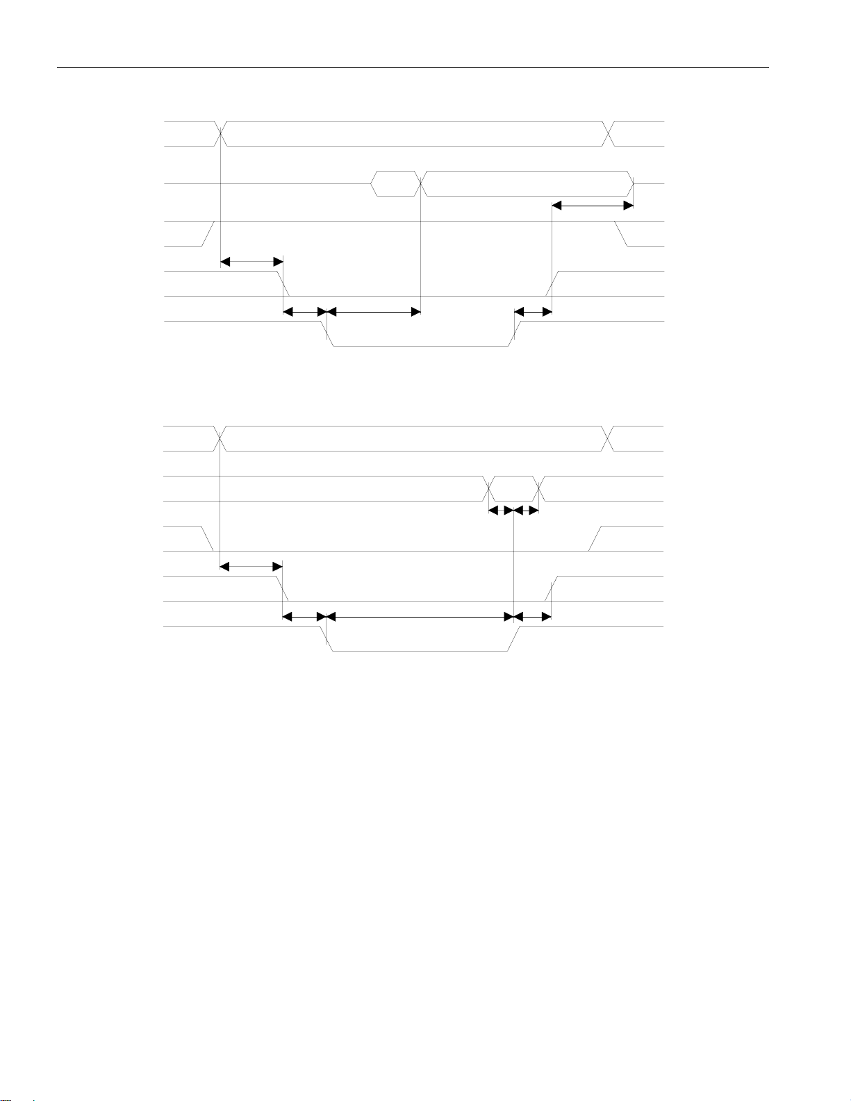
DS2148/Q48
MOTOROLA BUS READ TIMING (PBTS = 1, BIS1 = 0, BIS0 = 1) Figure 12-6
A0 to A4
D0 to D7
R/W*
t1
CS*
0ns min.
DS*
Address Valid
Data Valid
5ns min. / 20ns max.
0ns min.
t2 t3 t4
75ns max.
t5
0ns min.
MOTOROLA BUS WRITE TIMING (PBTS = 1, BIS1 = 0, BIS0 = 1) Figure 12-7
Address ValidA0 to A4
D0 to D7
10ns
R/W*
t1
CS*
0ns min.
DS*
0ns min.
t2 t6 t4
75ns min.
min.
t7
t8
10ns
min.
0ns min.
68 of 75
Page 69
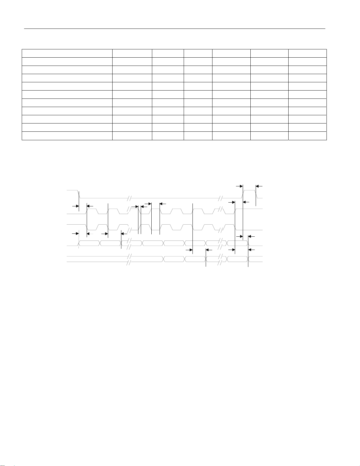
AC CHARACTERISTICS—SERIAL PORT
DS2148/Q48
(BIS1 = 1, BIS0 = 0)
(-40°C to +85°C; V
= 5.0V ± 5%)
DD
PARAMETER SYMBOL MIN TYP MAX UNITS NOTES
Setup Time CS* to SCLK t
Setup Time SDI to SCLK t
Hold Time SCLK to SDI t
SCLK High/Low Time t
SCLK Rise/Fall Time t
SCLK to CS* Inactive t
50 ns
CSS
50 ns
SSS
50 ns
SSH
200 ns
SLH
50 ns
SRF
50 ns
LSC
CS* Inactive Time tCM 250 ns
SCLK to SDO Valid t
SCLK to SDO 3-State t
CS* Inactive to SDO 3-State t
50 ns
SSV
100 ns
SSH
100 ns
CSH
See Figure 12-8
SERIAL BUS TIMING (BIS1 = 1, BIS0 = 0) Figure 12-8
t
CM
CS*
t
LSC
SCLK
t
t
SRF
t
1
CSS
SLH
2
SCLK
SDI
SDO
t
SSS
LSB MSB
NOTES:
1) OCES =1 and ICES = 0.
2) OCES = 0 and ICES = 1.
t
SSH
HIGH Z
MSB
LSB
LSB
t
CSH
t
SSV
MSB
t
SSH
HIGH Z
69 of 75
Page 70
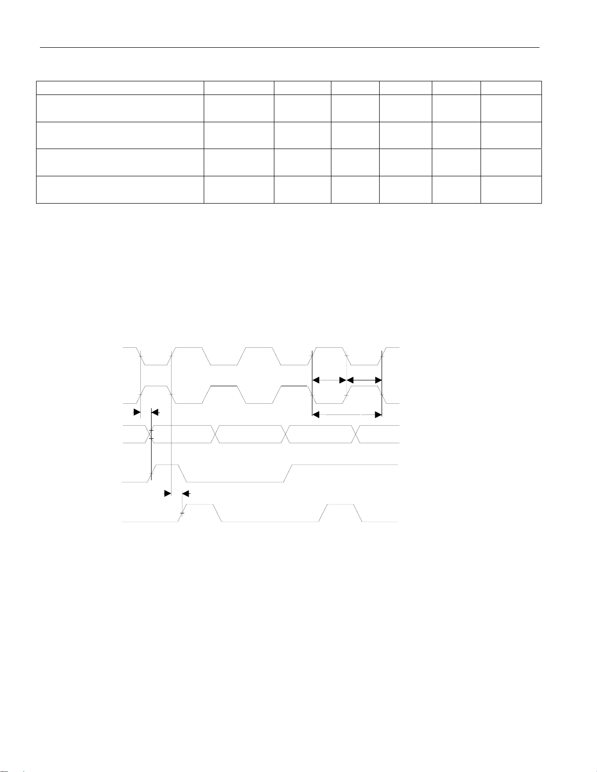
DS2148/Q48
AC CHARACTERISTICS—RECEIVE SIDE (-40°C to +85°C; VDD = 5.0V ± 5%)
PARAMETER SYMBOL MIN TYP MAX UNITS NOTES
RCLK Period tCP 488
648
RCLK Pulse Width tCH
tCL
RCLK Pulse Width tCH
tCL
Delay RCLK to RPOS, RNEG,
tDD 50 ns
200
200
150
150
ns
ns
ns
ns
ns
ns
1
2
3
3
4
4
PBEO, RBPV Valid
NOTES:
1) E1 Mode.
2) T1 or J1 Mode.
3) Jitter attenuator enabled in the receive path.
4) Jitter attenuator disabled or enabled in the transmit path.
RECEIVE SIDE TIMING Figure 12-9
1
RCLK
2
RCLK
t
DD
RPOS, RNEG
t
bit
error
DD
BPV/
EXZ/
CV
PBEO
3
RNEG
NOTES:
1) RCES = 1 (CCR2.0) or CES = 1.
2) RCES = 0 (CCR2.0) or CES = 0.
3) RNEG is in NRZ mode (CCR1.6 = 1).
t
CL
PRBS Detector Out of Sync
BPV/
EXZ/
CV
t
CP
t
CH
70 of 75
Page 71
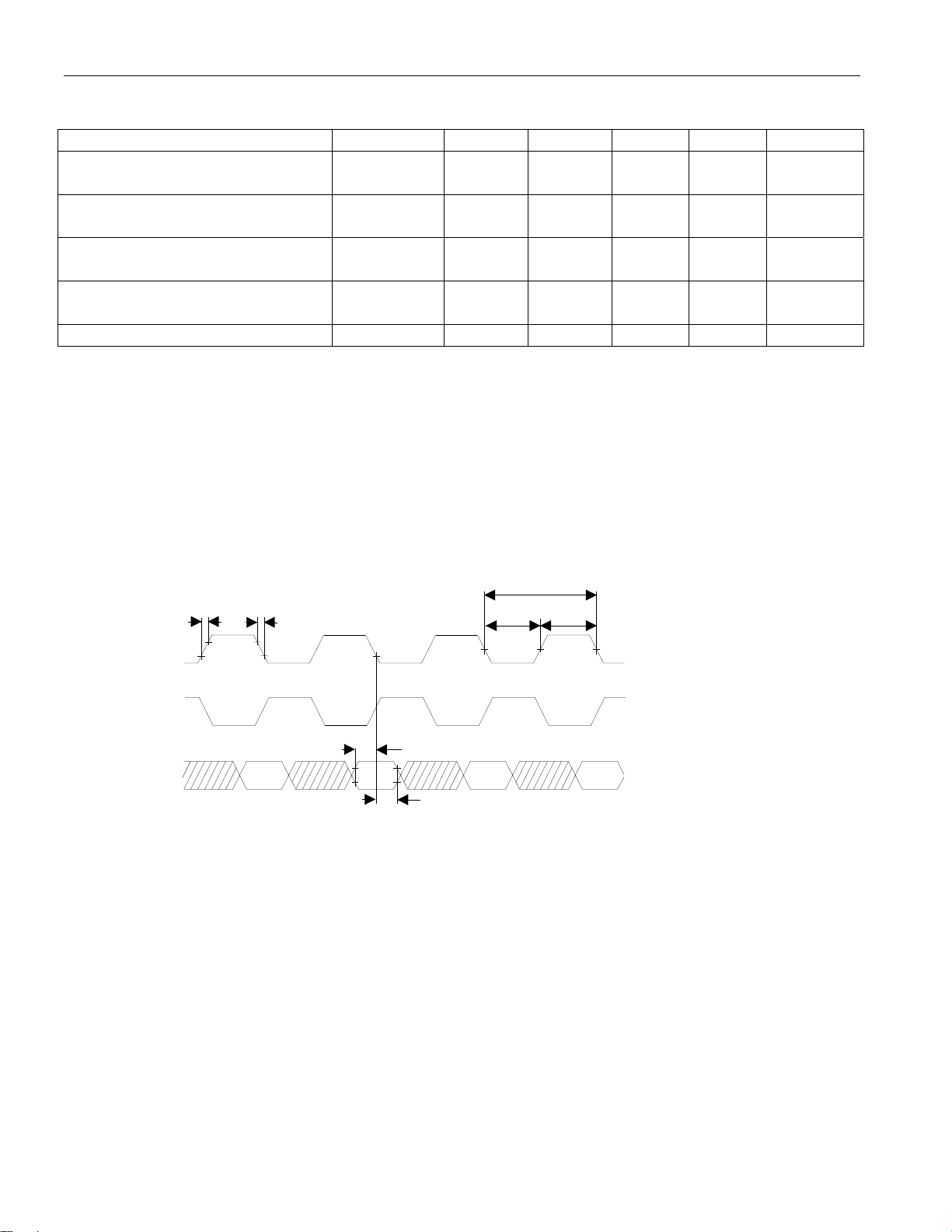
DS2148/Q48
AC CHARACTERISTICS—TRANSMIT SIDE (-40°C to +85°C; V
= 5.0V ± 5%)
DD
PARAMETER SYMBOL MIN TYP MAX UNITS NOTES
TCLK Period tCP 488
648
TCLK Pulse Width tCH
tCL
TPOS/TNEG Setup to TCLK
tSU 20 ns
75
75
ns
ns
ns
ns
1
2
Falling or Rising
TPOS/TNEG Hold From TCLK
tHD 20 ns
Falling or Rising
TCLK Rise and Fall Times tR, tF 25 ns
See Figure 12-10
NOTES:
1) E1 Mode.
2) T1 or J1 Mode.
TRANSMIT SIDE TIMING Figure 12-10
1
TCLK
2
TCLK
TPOS, TNEG
t
R
t
F
NOTES:
1) TCES = 0 (CCR2.1) or CES = 0.
2) TCES = 1 (CCR2.1) or CES = 1.
t
SU
t
HD
t
CL
t
CP
t
CH
71 of 75
Page 72
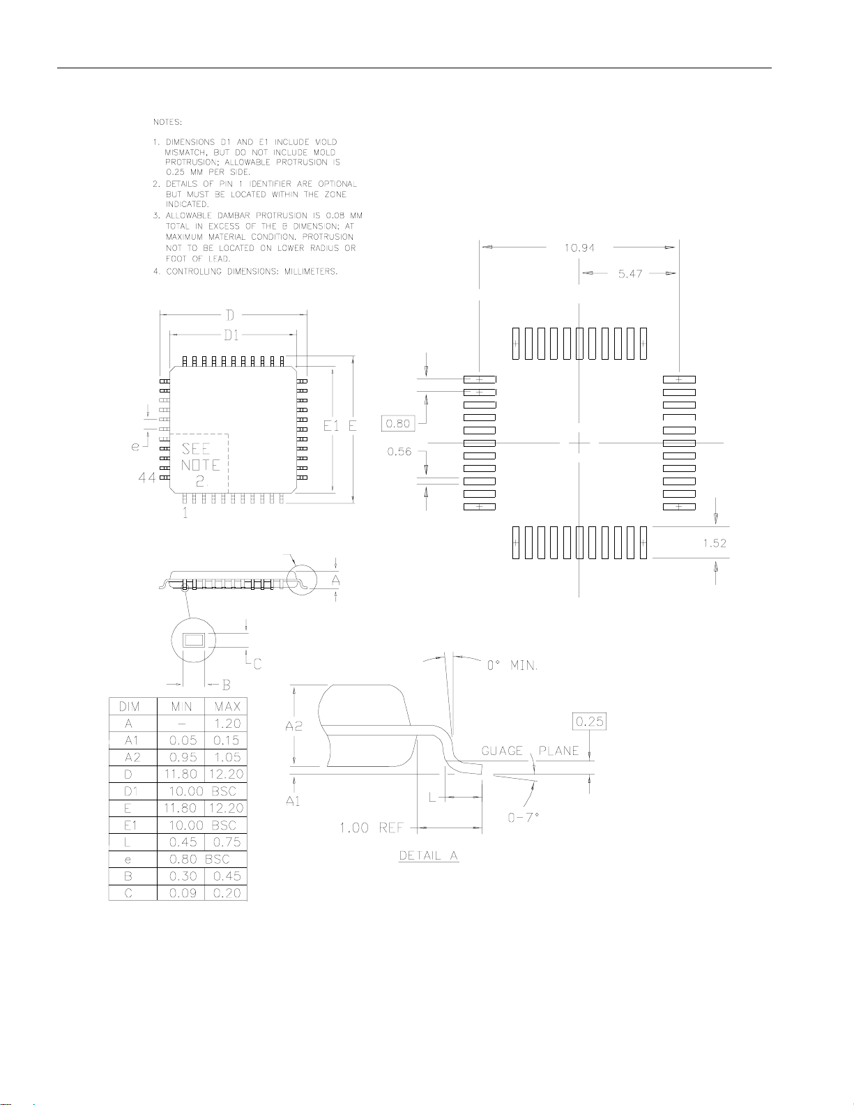
13. MECHANICAL DIMENSIONS
DS2148/Q48
SUGGESTED PAD LAYOUT
44 PIN TQFP, 10*10*1.0
SEE DETAIL "A"
DIMENSIONS ARE IN MILLIMETERS
72 of 75
Page 73
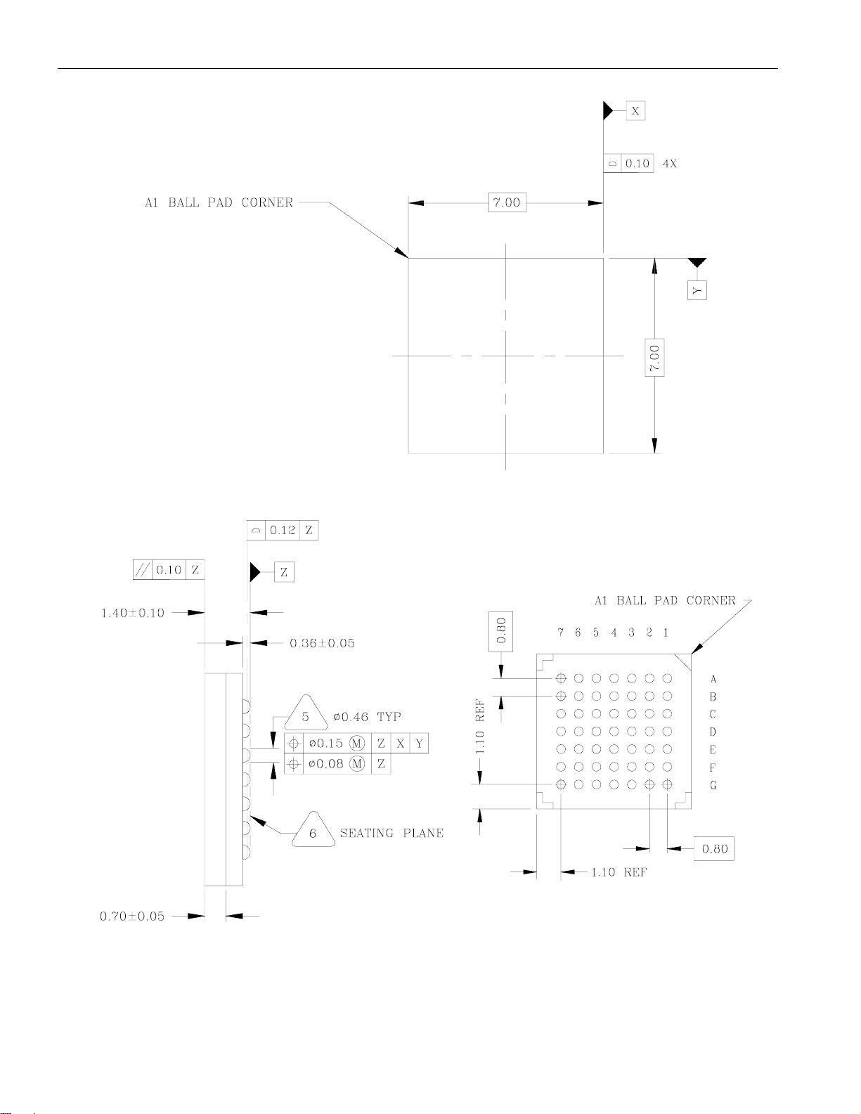
DS2148/Q48
73 of 75
Page 74
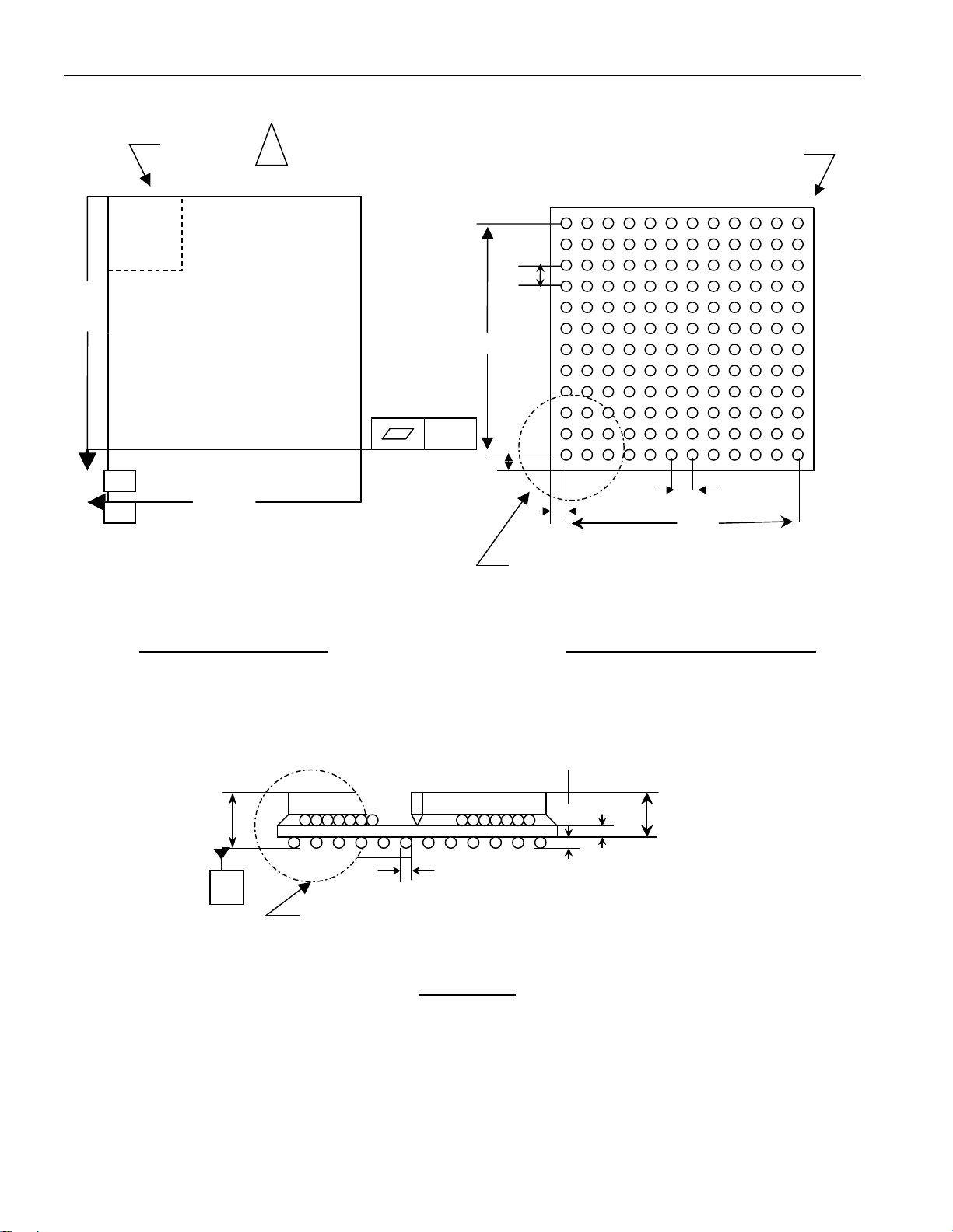
DS2148/Q48
13.1 Mechanical Dimensions—Quad Version
17.0
TOP VIEW (DIE SIDE) BOTTOM VIEW (BALL SIDE)
SIDE VIEW
A1
2.60
REF
17.0
Z
4
DETAIL B
0.20
0.76
13.97
1.52
1.27
DETAIL A
12 11 10 9 8 7 6 5 4 3 2
1.27
1.52
0.05
0.61
0.59
13.97
1.99
A1
A B C D E F G H I J K
74 of 75
Page 75
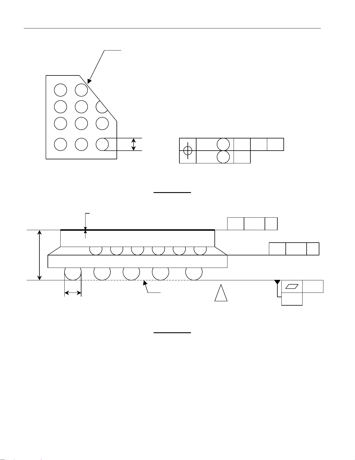
DS2148/Q48
/
f
L
f
L
SOLDER BALL
f 0.76 REF
0.76
0.76
X Z Y Z
DETAIL A
2.60
REF
0.76
REF
0.05 LABEL THICKNESS
SEATING PLANE
/
0.24 Z
/ /
0.17 Z
0.10
Z
DETAIL B
75 of 75
 Loading...