

Page 1
r
查询DS2117M供应商
www.dalsemi.com
DS2117M
Ultra3 LVD/SE SCSI Terminato
FEATURES
Fully compliant with Ultra2, Ultra3, and
Ultra 160/m SCSI
Provides Multimode Low Voltage
Differential/Single-Ended (LVD/SE)
termination for 9 signal line pairs
Auto-selection of LVD or SE termination
5% tolerance on SE and LVD termination
resistance
Low power down capacitance of 3 pF
Onboard thermal shutdown circuitry
SCSI bus hot plug compatible
Fully supports actively negated SE SCSI
signals
PIN ASSIGNMENT
VREF
R1P
R1N
R2P
R2N
HS GND
HS GND
HS GND
R3P
R3N
R4P
R4N
R5P
R5N
ISO
GND
1
NC
2
3
NC
4
5
6
7
8
9
10
11
12
13
14
15
16
17
18
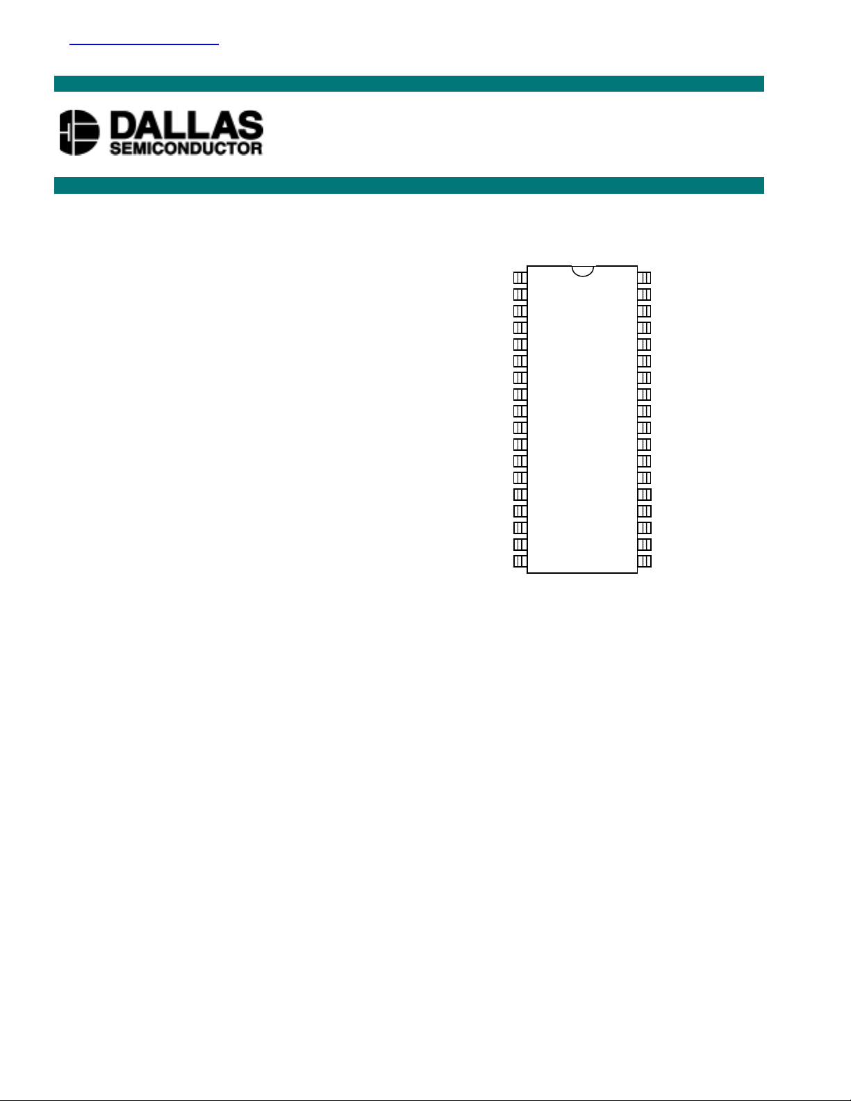
DS2117MB 36-Pin SSOP
36
35
34
33
32
31
30
29
28
27
26
25
24
23
22
21
20
19
TPWR
HVD
LVD
SE
R9N
R9P
R8N
R8P
HS GND
HS GND
HS GND
R7N
R7P
R6N
R6P
DIFF_CAP
DIFFSENSE
MSTR/SLV
DESCRIPTION
The DS2117M Ultra3 LVD/SE SCSI Terminator is both a Low Voltage Differential (LVD) and SingleEnded (SE) terminator. The multimode operation enables the designer to implement LVD in current
products while allowing the end-user SE backward compatibility with legacy devices. If the device is
connected in an LVD-only bus, the DS2117M will use LVD termination. If any SE devices are connect ed
to the bus, the DS2117M will use SE termination. This is accomplished automatically inside the part b y
sensing the voltage on the SCSI bus DIFFSENS line.
For the LVD termination, the DS2117M integrates two current sources with nine precision resistor
strings. For the SE termination, one regulator and nine precision 110-ohm resistors are used. Three
DS2117M terminators are needed for a wide SCSI bus.
1 of 9 090199
Page 2

DS2117M
REFERENCE DOCUMENTS
Small Computer Systems Interface (SCSI-3) SCSI Parallel Interface (SPI) Project: 0855-M, 1995
Small Computer Systems Interface (SCSI-3) SCSI Parallel Interface 2 (SPI-2) Project: 1142-M, 1998
Small Computer Systems Interface (SCSI-3) SCSI Parallel Interface 3 (SPI-3) Project: 1302-D, 1999
Small Computer Systems Interface (SCSI-3) SCSI Parallel Interface 4 (SPI-4) Project: 1365-D, xxxx
Available from:
American National Standards Institute (ANSI) Phone: (212) 642-4900
Global Engineering Documents 15 Inverness Way East; Englewood, CO 80112 Phone: (800) 854-7179
FUNCTIONAL DESCRIPTION
The DS2117 combines LVD and SE termination with DIFFSENSE sourcing and detection.
A bandgap reference is fed into two amplifiers, which creates a 1.25V reference voltage and a 2.85V
reference voltage. The control logic determines which of these references will be applied to the
termination resistors. If the SCSI bus is in LVD mode, then the 1.25V reference will be used. If the SCS I
bus is in SE mode, then the 2.85V reference will be used. That same control logic will switch in/out
parallel resistors to change the total termination resistance accordingly. Finally, in SE mode the Rp pins
will be switched to ground.
The DIFFSENSE circuitry decodes trinary logic. There will be one of three voltages on the SCSI control
line called DIFFSENS. Two comparators and a NAND gate determine if the voltage is below 0.6V, above
2.15V, or in between. That indicates the mode of the bus to be HVD, SE, or LVD, respectively.
The DS2117M’s DIFF_CAP pin monitors the DIFFSENS line to determine the proper operating mode of
the device; this mode is indicated by the SE/LVD/HVD outputs. The DIFFSENSE pin can also drive the
SCSI DIFFSENS line (when MSTR/SLV = 1) to determine the SCSI bus operating mode. The DS2117M
switches to the termination mode that is appropriate for the bus based on the value of the DIFFSENS
voltage. These modes are:
LVD mode LVD termination is provided by a precision laser trimmed resistor string with two current
sources. This configuration yields a 105Ω=differential and 150Ω=common mode impedance. A fail-safe
bias of 112 mV is maintained when no drivers are connected to the SCSI bus.
SE mode When the external driver for a given signal line turns off, the active terminator will pull that
signal line to 2.85 volts (quiescent state). When used with an active negation driver, the power amp can
sink 22 mA per line while keeping the voltage reference in regulation. The terminating resistors maintain
their 110Ω=value.
HVD Isolation Mode The DS2117M identifies that there is an HVD (high voltage di fferential) device on
the SCSI bus and isolates the termination pins from the bus.
When ISO is pulled high, the termination pins are isolated from the SCSI bus, Vref is grounded, and the
bus mode indicators (SE/LVD/HVD) remain active. During thermal shutdown, the termination pins are
isolated from the SCSI bus, Vref is grounded, and the bus mode indicators (SE/LVD/HVD) remain
active. The
DIFFSENSE driver is shut down during either of these two events.
2 of 9
Page 3

DS2117M
To ensure proper operation, the TPWR pin should be connected to the SCSI bus TERMPWR line. As
with all analog circuitry, the TERMPWR and VDD lines should be bypassed locally. A 2.2 µF capacitor
and a 0.01 µF high frequenc y capacitor is recommended between TPW R and ground and placed as close
as possible to the DS2117M. The DS2117M should be placed as close as possible to the SCSI conne ctor
to minimize signal and power trace length, thereby resulting in less input capacitance and reflections
which can degrade the bus signals.
To maintain the specified regulation, a 4.7 µF capacitor is required between the Vref pin (VREF) and
ground of each DS2117M. A high frequency cap (0.1 µF ceramic recomm ended) can also be placed on
the Vref pin in applications that use fast rise/fall time drivers. A typical SCSI bus configuration is shown
in Figure 2.
DIFFSENS noise filtering The DS2117M incorporates a digital filter to remove high frequency
transients on the DIFFSENS control line, thereby eliminating erroneous switching between modes. This
filter eliminates the need for the external capacitor and resistor, which heretofore performed this function.
The external filter may be used in addition to the digital filter if the DS2117M and DS2118M are to be
used interchangeably.
NOTE:
DIFFSENS – Refers to the SCSI bus signal.
DIFFSENSE – Refers to the DS2117M pin name and internal circuitry capable of driving the
DIFFSENS line.
DIFF_CAP - Refers to the DS2117M pin name and internal circuitry relating to monitoring the
DIFFSENS line.
3 of 9
Page 4

DS2117M BLOCK DIAGRAM Figure 1
DS2117M
4 of 9
Page 5

SCSI BUS CONFIGURATION Figure 2
DS2117M
5 of 9
Page 6

PIN DESCRIPTION Table 1
PIN SYMBOL DESCRIPTION
1VREFReference Voltage. 2.85 volt reference in SE mode and 1.25 volt
reference in LVD mode; must be decoupled with a 4.7 µF cap.
2, 3 NC No Connect. Do not connect these pins.
4-7, 11-16,
22-25, 29-32
8, 10, 26,
9, 28, 27
17 ISO Isolation. When pulled high, the DS2117M isolates its bus pins (RxP,
18 GND Ground. Signal ground; 0.0 volts.
19 MSTR/SLV Master/slave. Mode select for the non-controlling terminator. When
20 DIFFSENSE DIFFSENSE. Output to drive the SCSI bus DIFFSENS line.
21 DIFF_CAP DIFFSENSE CAPACITOR. Connect 0.1 µF capacitor for
33 SE Single-ended. SE output of DIFFSENSE receiver; output high
34 LVD Low Voltage Differential. LVD output of DIFFSENSE receiver;
35 HVD High Voltage Differential. HVD output of DIFFSENSE receiver;
36 TPWR Termination Power. Connect to the SCSI TERMPWR line and
RxP
Signal Termination. Connect to SCSI bus signal lines.
RxN
HS GND Heat Sink Ground. Internally connected to the mounting pad. Should
be grounded.
RxN) from the SCSI bus.
pulled high (MSTR), the DIFFSENSE driver is enabled.
DIFFSENSE filter. Input to detect the type of device (differential or
single-ended) on the SCSI bus.
indicates SE bus operation.
output high indicates LVD bus operation.
output high indicates HVD bus operation or thermal shutdown.
decouple with 2.2 µF capacitor.
DS2117M
RECOMMENDED OPERATING CONDITIONS
PARAMETER SYMBOL MIN TYP MAX UNITS NOTES
SE mode
Termpower Voltage
LVD mode
Logic 0 V
Logic 1 V
Operating Temperature V
V
V
tpwr
(SE)
tpwr
(LVD)
ih
amb
4.0
2.7
il
-0.3 +0.8 V
2.0 V
5.5
5.5
+ 0.3 V
tpwr
V
V
070°C
6 of 9
Page 7

DS2117M
SINGLE ENDED CHARACTERISTICS
PARAMETER SYMBOL MIN TYP MAX UNITS NOTES
SE Termination Resistance
SE Voltage Reference
SE Output Current
Output Capacitance
Rse 104.5 110 115.5 Ohms 1
Vref 2.7 3.0 Volts
lose 25.4 mA 2
Cout 3 pF 3
LOW VOLTAGE DIFFERENTIAL CHARACTERISTICS
PARAMETER SYMBOL MIN TYP MAX UNITS NOTES
Differential Mode
Termination Resistance
Common Mode
Termination Resistance
Differential Mode Bias
Common Mode Bias
Rdm 100 110 Ohms
Rcm 110 190 Ohms
Vdm 100 125 mV 4
Vcm 1.125 1.375 V
DC CHARACTERISTICS
PARAMETER SYMBOL MIN TYP MAX UNITS NOTES
Termpower Current
Input Leakage High
Input Leakage Low
Output Current High
Output Current Low
DIFFSENS SE
Operating Range
DIFFSENS LVD
Operating Range
DIFFSENS HVD
Operating Range
DIFFSENSE Driver
Output Voltage
DIFFSENSE Driver
Source Current
DIFFSENSE Driver
Sink Current
Thermal Shutdown
V
V
I
V
V
I
I
tpmr
I
ih
I
il
I
oh
I
ol
seor
lvdor
hvdor
dso
dsh
dsl
12 mA 4
-1.0 µA
1.0 µA
-1.0 mA 5, 7
4.0 mA 6, 7
-0.3 0.5 V
0.7 1.9 V
V
2.4
tpwr
+ 0.3
V
1.2 1.4 V 8, 9
5 15 mA 8, 10, 12
20 200 µA 8, 11
150 ºC 3
7 of 9
Page 8

DS2117M
REGULATOR CHARACTERISTICS
PARAMETER SYMBOL MIN TYP MAX UNITS NOTES
Line Regulation
Load Regulation
Current Limit
Sink Current
LI
LO
I
I
REG
REG
LIM
SINK
1.0 2.5 %
1.3 3.5 %
550 mA
200 mA
NOTES:
1. Vline = 0-3.0 volts.
2. Vline = 0.2 volts.
3. Guaranteed by design.
4. All lines open.
5. V
6. V
7. SE/LVD/HVD pins only.
8. MSTR/SLV = 1.
9. Ids = 0-5 mA.
10. V
11. V
12. TPWR = 5.5V
= 2.4 volts.
OUT
= 0.4 volts.
OUT
= 0.0 volts.
dso
= 2.75 volts.
dso
8 of 9
Page 9

DS2117M 36-PIN SSOP PACKAGE
DIMENSIONS D AND E1 INCLUDE MOLD MISMATCH, BUT DO NOT
INCLUDE MOLD FLASH, PROTRUSIONS OR GATE BURRS. MOLD
FLASH, PROTRUSIONS OR GATE BURRS SH ALL NOT EXCEED 0.254
MM PER SIDE.
SECTION A-A DIMENSIONS APPLY TO THE FLAT SECTION OF THE
LEAD BETWEEN 0.13 TO 0.25 MM FROM THE LEAD TIP.
THE CHAMFER ON THE BODY IS OPTIONAL. IF IT IS NOT PRESENT,
A VISUAL INDEX FEATURE MUST BE LOCATED WITHIN THE
CROSS-HATCHED ARE A.
DS2117M
DIM MIN MAX
A 2.44 2.64
A1 0.12 -
b 0.29 0.43
c 0.23 0.32
D 15.20 15.54
E 10.11 10.52
E1 7.40 7.60
e 0.80 BSC
h 0.25 0.71
L 0.51 1.02
DIMENSIONS ARE IN MILLIMETERS
CSP option - mechanical drawing
Please check the following web location for latest information on our Chip Scale Package (a.k.a
"solder bump") "http://www.dalsemi.com/DocControl/Chips/index.html"
9 of 9
 Loading...