

Page 1
r
www.dalsemi.com
(
)
DS2108
Differential SCSI Switchable Terminato
FEATURES
PIN ASSIGNMENT
Fully compliant with SCSI, SCSI-2 and SCSI-
3 standards
Conforms to EIA RS-485 standard
Provides differential termination for 9 pairs of
signal lines
Operates with SCSI signal voltages of -7 to
+12 Volts
Laser-trimmed 330 and 150-ohm termination
resistors have ±5% tolerance over full
temperature range
Switchable power-down mode
Low power down capacitance of 6 pF
24-pin plastic SOIC (DS2108S)
TPWR
R1N
R2N
R3N
R4N
R5N
R6N
R7N
R8N
R9N
TPWR
NC
DS2108S 24-Pin SOIC
1
2
3
4
5
6
7
8
9
10
11
12
24
23
22
21
20
19
18
17
16
15
14
13
300-mil
PD
GND
R1P
R2P
R3P
R4P
R5P
R6P
R7P
R8P
R9P
GND
DESCRIPTION
The DS2108 SCSI Terminator has been specifically designed for High Voltage Differential (HVD) SCSI
systems requiring switchable termination. The DS2108 integrates eighteen 330-ohm and nine 150-ohm
precise switched termination resistors into a monolithic IC. The surface mount SOIC package saves board
space over conventional resistor SIPs. The termination resistors can be isolated from the SC SI bus under
software or hardware control. While in the powered down mode, the DS2108 isolates the nine terminator
blocks from the bus while adding only 6 pF capacitance to each signal line of the SCSI bus.
FUNCTIONAL DESCRIPTION
The DS2108 consists of power-down circuitry, eighteen 330-ohm and nine 150-ohm termination resistors
(Figure 1). The DS2108 can be removed from the circuit by bringing the power down pin (PD) low. The
power down capacitance on the terminating resistors is 6 pF, well below the SCSI-3 allotment of 25 pF.
The DS2108 supports SCSI signal voltages of -7 to +12 volts when powered on or off. When all lines
settle into the quiescent state (no signal transitions), 56 mA is typically consumed. Only 1 mA is
typically consumed in the powered down mode.
1 of 5 112099
Page 2
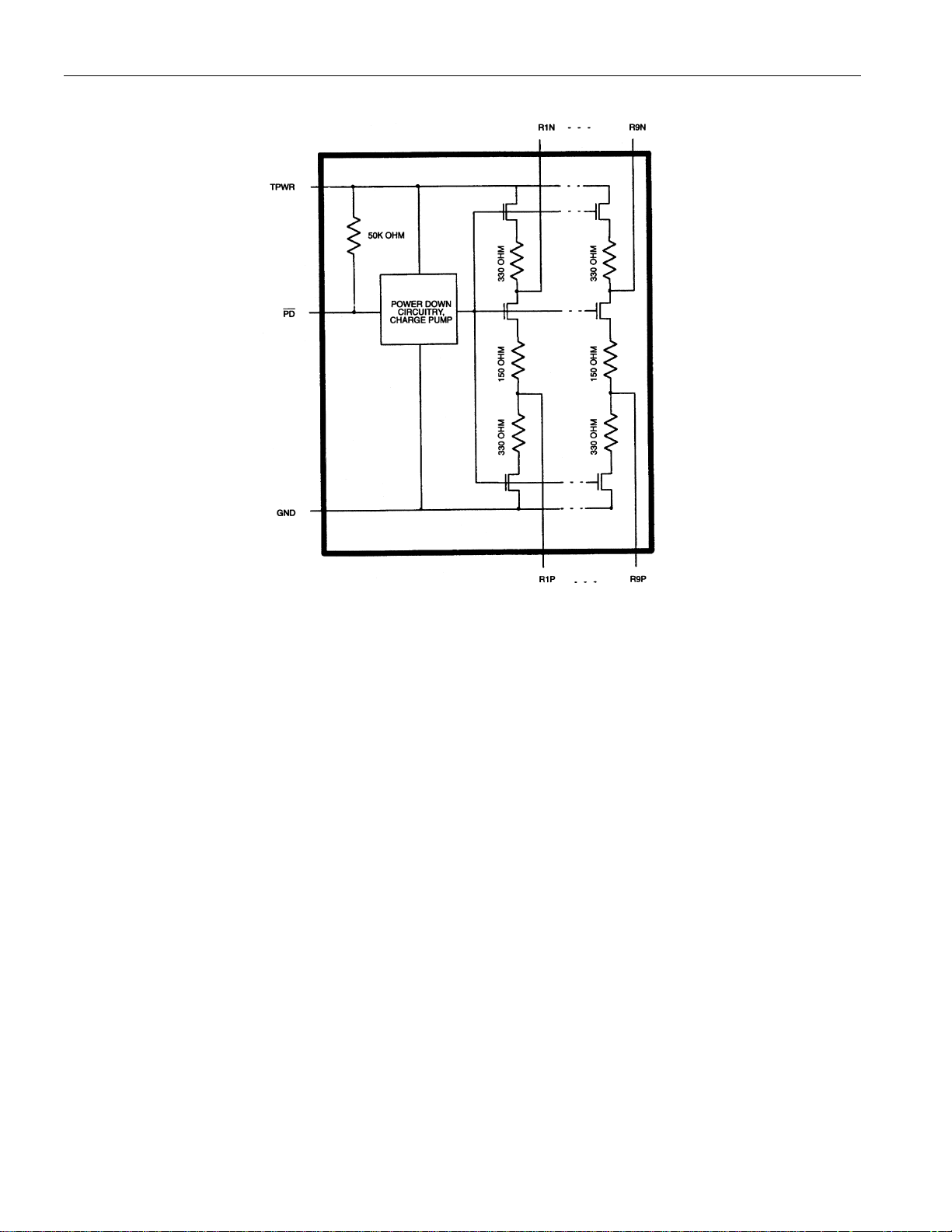
DS2108 BLOCK DIAGRAM Figure 1
DS2108
2 of 5
Page 3

TYPICAL DIFFERENTIAL SCSI BUS CONFIGURATION Figure 2
NOTES:
1. Two DS2108s required per 8–bit SCSI device and three DS2108s per 16–bit SCSI device.
DS2108
2. Mid–bus termination effectively removed by grounding PD pin.
3. Termination power to be provided as specified in SCSI–3 Parallel Interface (SPI) document.
4. Local TERMPWR bypassing is recommended by the SPI document with values shown. The bypass
capacitors should be located as close as possible to the DS2108s. Only one pair of capacitors is
required per SCSI device (may be shared between DS2108s on same device).
PIN DESCRIPTION Table 1
PIN SYMBOL DESCRIPTION
1, 11 TPWR Termination Power. Should be connected to the SCSI TERMPWR line.
Bypass with a 2.2 µF cap in parallel with a 0.1 µF cap as shown in Figure
2.
2, 3, 4, 5, 6,
7, 8, 9, 10
12 NC No Connect. Do not connect any signal to this pin.
13, 23 GND Ground. Signal ground; 0.0V.
14, 15, 16,
17, 18, 19,
20, 21, 22
24
R1N…R9N Signal Termination Negative. Connect to –SIGNAL of SCSI bus.
R1P…R9P Signal Termination Positive. Connect to +SIGNAL of SCSI bus.
PD
Power Down. When tied low, the DS2108 enters a power-down mode.
Contains an internal 50K pull-up. Strap low to deactivate the DS2108,
leave open circuited to activate the DS2108.
3 of 5
Page 4

DS2108
ABSOLUTE MAXIMUM RATINGS*
Voltage on Any Pin Relative to Ground -7.0V to +12.0V
Operating Temperature 0°C to 70°C
Storage Temperature -55°C to +125°C
Soldering Temperature 260°C for 10 seconds
* This is a stress rating only and functional operation of the device at these or any other conditions above
those indicated in the operation sections of this specification is not implied. Exposure to absolute
maximum rating conditions for extended periods of time may affect reliability.
RECOMMENDED OPERATING CONDITIONS (0°C to 70°C)
PARAMETER SYM MIN TYP MAX UNITS NOTES
TERMPWR Voltage V
PD Active
PD Inactive
V
V
TP
PDA
PDI
4.00 5.25 V
-0.3 0.8 V
2.00 VTP +
V
0.3
DC CHARACTERISTICS
PARAMETER SYMBOL MIN TYP MAX UNITS NOTES
TERMPWR Current I
Power-down Current I
Command Mode
Voltage
Termination Resistance R
Termination Resistance R
Termination Resistance R
Power-down
Termination
Capacitance
V
C
TP
PD
em
TTN
TNP
TPG
PD
7.0 12.0 V 7, 8
313.5 330 346.5 ohms 2
142.5 150 157.5 ohms 3
313.5 330 346.5 ohms 4
56 65 mA 1, 6
1 2 mA 1, 5
5 6 pF 1, 5, 7
NOTES:
1. 4.00V < TERMPWR < 5.25V
2. 330 Ω=resistor between TERMPWR and -SIGNAL.
3. 150 Ω=resistor between -SIGNAL and +SIGNAL.
4. 330 Ω=resistor between +SIGNAL and GDN.
5.
PD = 0.0V.
6. Signal pins left open.
7. Guaranteed by design; not production tested.
8. Signal lines RxN and RxP only.
4 of 5
Page 5

24-PIN SOIC (300-MIL)
DS2108
The chamfer on the body is optional. If it is not present, a terminal 1 identifier must be positioned so that
½ or more of its area is contained in the hatched zone.
PKG 24-PIN
DIM MIN MAX
A IN.
MM
A1 IN.
MM
A2 IN.
MM
b IN.
MM
C IN.
MM
D IN.
MM
e IN.
MM
E1 IN.
MM
H IN.
MM
L IN.
MM
ΘΘΘΘ
0.094
2.38
0.004
0.102
0.089
2.26
0.013
0.33
0.009
0.229
0.598
15.19
0.050 BSC
1.27 BSC
0.290
7.37
0.398
10.11
0.016
0.40
0° 8°
0.105
2.68
0.012
0.30
0.095
2.41
0.020
0.51
0.013
0.33
0.612
15.54
0.300
7.62
0.416
10.57
0.040
1.02
5 of 5
 Loading...