

Page 1
查询DS2107A供应商
DS2107A
DS2107A
SCSI Terminator
FEATURES
• Fully compliant with SCSI and SCSI-2 standards
• Backward compatible to the DS2107S
• Provides active termination for 9 signal lines
• Laser-trimmed 110 ohm termination resistors have
1% tolerance
• Low dropout voltage
• Power-down mode isolates termination resistors from
the bus
• Handles actively negated SCSI signals
• Onboard thermal shutdown circuitry
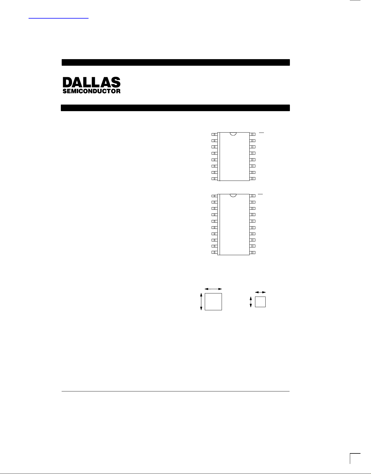
• 16-pin plastic SOIC (DS2107AS) and 20-pin plastic
thin SSOP (DS2107AE)
PIN ASSIGNMENT
TERMPWR1
VREF1
GND
TERMPWR1
HS–GND
HS–GND
VREF1
GND
1
2
R1
R2
3
R3
4
5
R4
R5
6
7
8
DS2107AS 16-Pin SOIC (300 mil)
1
2
R1
3
R2
4
R3
5
R4
6
R5
7
8
9
10 11
DS2107AE 20-Pin TSSOP (173 mil)
ACTUAL FOOTPRINT SIZE
.41”
16
15
14
13
12
11
10
20
19
18
17
16
15
14
13
12
9
PD
VREF2
NC
R9
R8
R7
R6
TERMPWR2
PD
VREF2
HS–GND
NC
R9
R8
R7
R6
HS–GND
TERMPWR2
.26”
DESCRIPTION
The SCSI-2 standard recommends the use of active terminations at both ends of every cable segment in a
SCSI system with single-ended drivers and receivers.
The DS2107A SCSI T erminator , which is fully compliant
with the standard, enables the designer to gain the
benefits of active termination: greater immunity to voltage drops on the TERMPWR (TERMination PoWeR)
.41”
.27”
DS2107AS DS2107AE
line, enhanced high-level noise immunity, intrinsic
TERMPWR decoupling, and very low quiescent current
consumption. The DS2107A integrates a regulator and
nine precise switched 110 ohm termination resistors
into a monolithic IC.
022698 1/7
Page 2
DS2107A
FUNCTIONAL DESCRIPTION
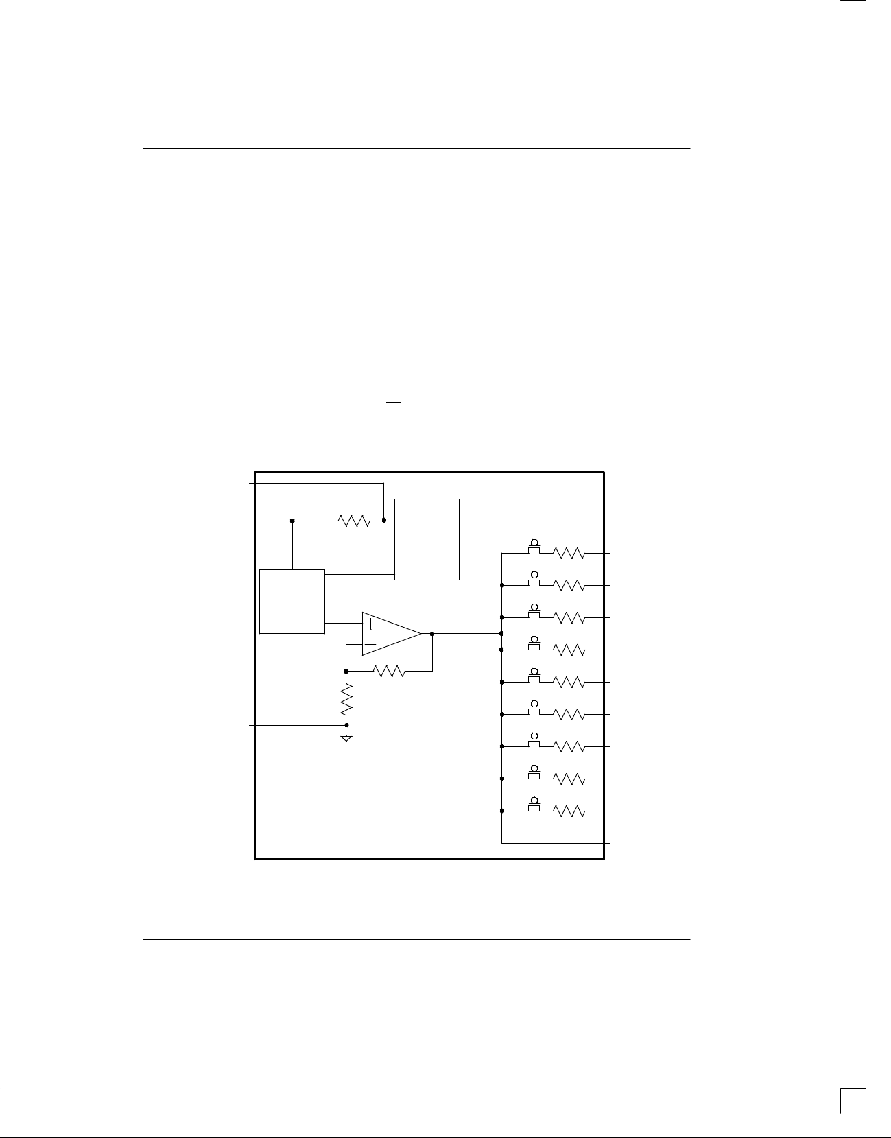
The DS2107A consists of a bandgap reference, buffer
amplifier, and nine termination resistors (Figure 1). The
bandgap reference circuit produces a precise 2.55V
level which is fed to a buffer amplifier. The buffer produces a 2.85V level and is capable of sourcing at least
24 mA into each of the termination resistors when the
signal line is low (active). When the driver for a given
signal line turns off, the terminator will pull the signal line
to 2.85V (quiescent state). To handle actively negated
SCSI signals, the buffer can sink 200 mA. When all lines
settle in the quiescent state, the regulator will consume
about 5 mA. When the DS2107A is put into powerdown mode by bringing PD
low, the power-down circuitry will turn off the transistors on each signal line. This will
isolate the DS2107A from the signal lines and effectively remove it from the circuit. The power-down pin (PD)
DS2107A BLOCK DIAGRAM Figure 1
PD
TERMPWR1
TERMPWR2
GND
Bandgap
Reference
50K Ohm
has an internal 50K ohm pull-up resistor. To place the
DS2107A into an active state, the PD
pin should be left
open circuited.
T o ensure proper operation, both the TERMPWR1 and
TERMPWR2 pins must be connected to the SCSI bus
TERMPWR line and both the VREF1 and VREF2 pins
must be tied together externally. Each DS2107A requires parallel 0.1 µF and 4. 7 µF capacitors connected
between the VREF pins and ground. Figure 2 details a
typical SCSI bus configuration. In an 8-bit wide SCSI
bus arrangement (“A” Cable), two DS2107A’ s would be
needed at each end of the SCSI cable in order to terminate the 18 active signal lines. In a 16-bit wide SCSI bus
arrangement (“P” Cable), three DS2107A’s would be
needed at each end of the SCSI cable in order to terminate the 27 active signal lines.
Power
Down
Circuitry
110 Ohms
110 Ohms
110 Ohms
110 Ohms
110 Ohms
110 Ohms
110 Ohms
110 Ohms
110 Ohms
R1
R2
R3
R4
R5
R6
R7
R8
R9
022698 2/7
VREF1
VREF2
Page 3
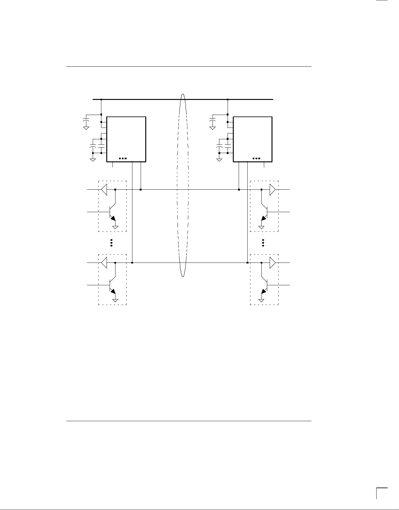
TYPICAL SCSI BUS CONFIGURATION Figure 2
Termination Power Line
DS2107A
C3
+
C1
C2
DS2107A
TERMPWR1
TERMPWR2
VREF1
+
VREF2
GND
R1 R2R9
R8
SCSI
Bus
Transceiver
SCSI
Cable
C3
+
+
C1
C2
SCSI
Bus
Transceiver
DS2107A
TERMPWR1
TERMPWR2
VREF1
VREF2
GND
R1 R9
SCSI
Bus
Transceiver
SCSI
Bus
Transceiver
NOTES:
1. C1 = 0.1µF ceramic
C2 = 4.7µF tantalum
C3 = 2.2 µF tantalum or 4.7 µF aluminum
2. If the DS2107A is to be embedded into a peripheral that will act as a target on a SCSI bus, it is recommended
that TERMPWR be derived from the SCSI cable, not generated locally. In this configuration, if a power failure
occurs in the peripheral, it will not affect the bus.
022698 3/7
Page 4

DS2107A
PIN DESCRIPTION Table 1
DS2107AE
PIN
1 1 TERMPWR1 Termination Power 1. Should be connected to the SCSI
3 2 R1 Signal Termination 1. 110 ohm termination.
4 3 R2 Signal Termination 2. 110 ohm termination.
5 4 R3 Signal Termination 3. 110 ohm termination.
6 5 R4 Signal Termination 4. 110 ohm termination.
7 6 R5 Signal Termination 5. 110 ohm termination.
9 7 VREF1 Reference Voltage 1. Must be externally connected directly to
10 8 GND Ground. Signal ground; 0.0V .
11 9 TERMPWR2 Termination Power 2. Should be connected to the SCSI
13 10 R6 Signal Termination 6. 110 ohm termination.
14 11 R7 Signal Termination 7. 110 ohm termination.
15 12 R8 Signal Termination 8. 110 ohm termination.
16 13 R9 Signal Termination 9. 110 ohm termination.
17 14 NC No Connect. Do not connect any signal to this pin.
19 15 VREF2 Reference Voltage 2. Must be externally connected directly to
20 16 PD Power Down. When tied low, the DS2107A enters a power-down
2,8,12,18 N/A HS–GND Heat Sink Ground. Internally connected to the mounting pad.
DS2107AS
PIN
SYMBOL DESCRIPTION
TERMPWR line. Must be decoupled with either a 2.2µF or 4.7µF.
See Figure 2.
the VREF2 pin. Must be decoupled with a 4.7µF and a 0.1µF as
shown in Figure 2.
TERMPWR line. Must be decoupled with either a 2.2µF or 4.7µF.
See Figure 2.
the VREF1 pin. Must be decoupled with a 4.7µF and a 0.1µF as
shown in Figure 2.
mode. Contains an internal 50K pull-up. Strap low to deactivate
the DS2107A, leave open circuited to activate the DS2107A.
Should be either grounded or electrically isolated from other circuitry.
022698 4/7
Page 5
DS2107A
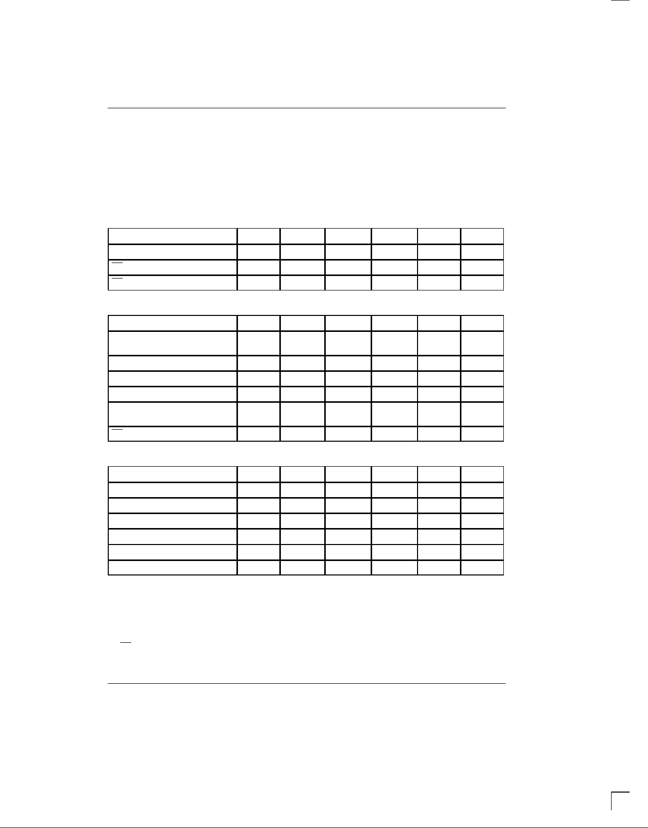
ABSOLUTE MAXIMUM RATINGS*
Voltage on Any Pin Relative to Ground -1.0V to +7.0V
Operating Temperature 0°C to +70°C
Storage Temperature -55°C to 125°C
Soldering Temperature 260°C for 10 seconds
* This is a stress rating only and functional operation of the device at these or any other conditions above
those indicated in the operation sections of this specification is not implied. Exposure to absolute maximum rating conditions for extended periods of time may affect reliability.
RECOMMENDED OPERATING CONDITIONS (0°C to 70°C)
PARAMETER SYMBOL MIN TYP MAX UNITS NOTES
TERMPWR Voltage V
PD Active V
PD Inactive V
TP
PDA
PDI
4.00 5.25 V
-0.3 0.8 V
2.0 VTP +0.3 V
DC CHARACTERISTICS (0°C to 70°C)
PARAMETER SYMBOL MIN TYP MAX UNITS NOTES
TERMPWR Current I
Power Down Current I
T ermination Resistance R
Die Thermal Shutdown T
Power Down Termination
Capacitance
PD Hysteresis H
TP
I
TP
PD
TERM
SD
C
PD
PD
5
100 µA 1,2,5
108 110 112 ohms 1,2
150 °C 1
8.5 10 pF 1,2,5,6
280 mV 1
250
8
mA
mA
1,3
1,4
REGULATOR CHARACTERISTICS (0°C to 70°C)
PARAMETER SYMBOL MIN TYP MAX UNITS NOTES
Output Voltage V
Drop Out Voltage V
Line Regulation LI
Load Regulation LO
Current Limit I
Sink Current I
REF
DROP
REG
REG
LIM
SINK
2.79 2.85 2.91 V 1,2
0.75 1.0 V 3,6
1.0 2.0 % 1,4,6
1.3 3.0 % 1,2,6
300 350 400 mA 1
200 mA 1
NOTES:
1. 4.00V < TERMPWR < 5.25V .
2. 0.0V < signal lines < 3.0V .
3. All signal lines = 0.0V .
4. All signal lines open.
5. PD
= 0.0V.
6. Guaranteed by design; not production tested.
022698 5/7
Page 6
DS2107A
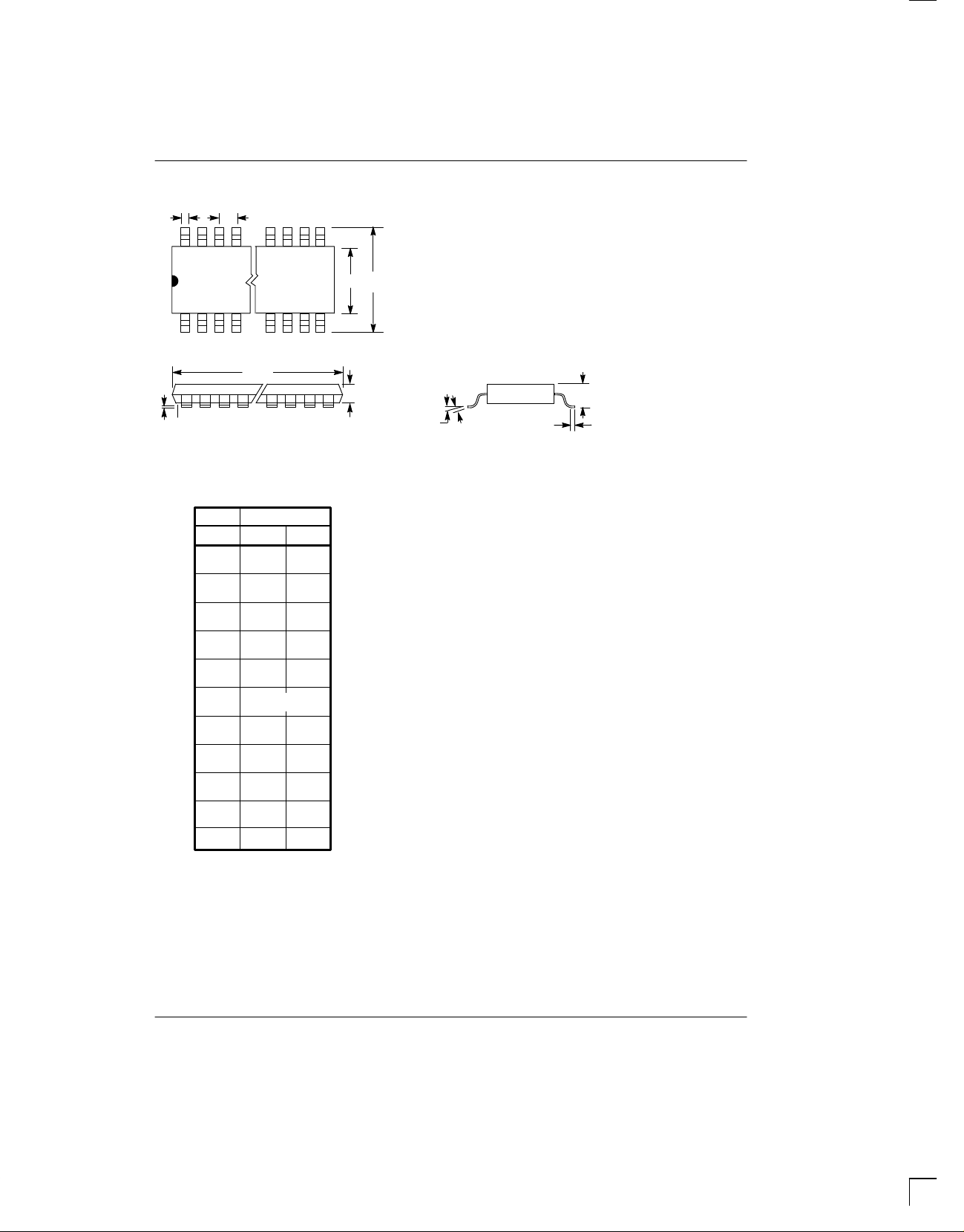
DS2107AS SCSI TERMINATOR 16-PIN SOIC (300 MIL)
GK
HB
1
A
C
F
E
16-PINPKG
DIM MIN MAX
A IN.
0.402
10.21
0.290
7.37
0.089
2.26
0.004
0.102
0.094
2.38
0.050 BSC
1.27 BSC
0.398
10.11
0.009
0.229
0.013
0.33
0.40
0° 8°
0.412
10.46
0.300
7.65
0.095
2.41
0.012
0.30
0.105
2.68
0.416
10.57
0.013
0.33
0.019
0.48
0.040
1.02
MM
B IN.
MM
C IN.
MM
E IN.
MM
F IN.
MM
G IN.
MM
H IN.
MM
J IN.
MM
K IN.
MM
L IN.MM0.016
phi
phi
J
L
022698 6/7
Page 7
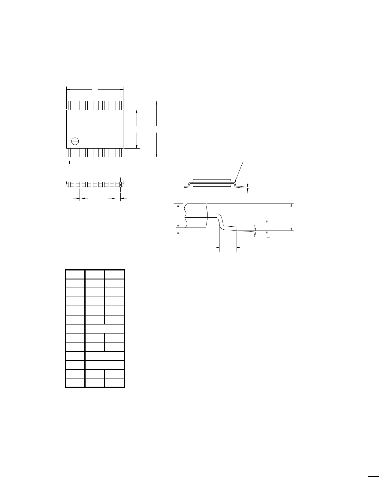
DS2107AE SCSI TERMINATOR 20-PIN TSSOP (PRELIMINARY)
D
n
DS2107A
B
e1
DIM MIN MAX
A MM – 1.10
A1 MM 0.05 –
A2 MM 0.75 1.05
C MM 0.09 0.18
L MM 0.50 0.70
e1 MM 0.65 BSC
B MM 0.18 0.30
D MM 6.40 6.90
E MM 4.40 NOM
G MM 0.25 REF
H MM 6.25 6.55
phi 0° 8°
E
H
SEE DETAIL A
c
A2
A1
L
DETAIL A
phi
G
A
022698 7/7
 Loading...