

Page 1
1 of 9 092399
FEATURES
§ Low-power CMOS design
§ Standby current
− 50 nA max at tA = 25°C VCC = 3.0V
− 100 nA max at tA = 25°C VCC = 5.5V
− 1 µA max at tA = 60°C VCC = 5.5V
§ Full operation for VCC = 5.5V to 2.7V
§ Data retention voltage = 5.5V to 2.0V
§ Fast 5V access time
− DS2016 - 100 100 ns
− DS2016 - 150 150 ns
§ Reduced-speed 3V access time
− DS2016 - 100 250 ns
− DS2016 - 150 250 ns
§ Operating temperature range of -40°C to
+85°C
§ Full static operation
§ TTL compatible inputs and outputs over
voltage range of 5.5V to 2.7 volts.
§ Available in 24-pin DIP and 24-pin SOIC
packages
§ Suitable for both battery operated and battery
backup applications
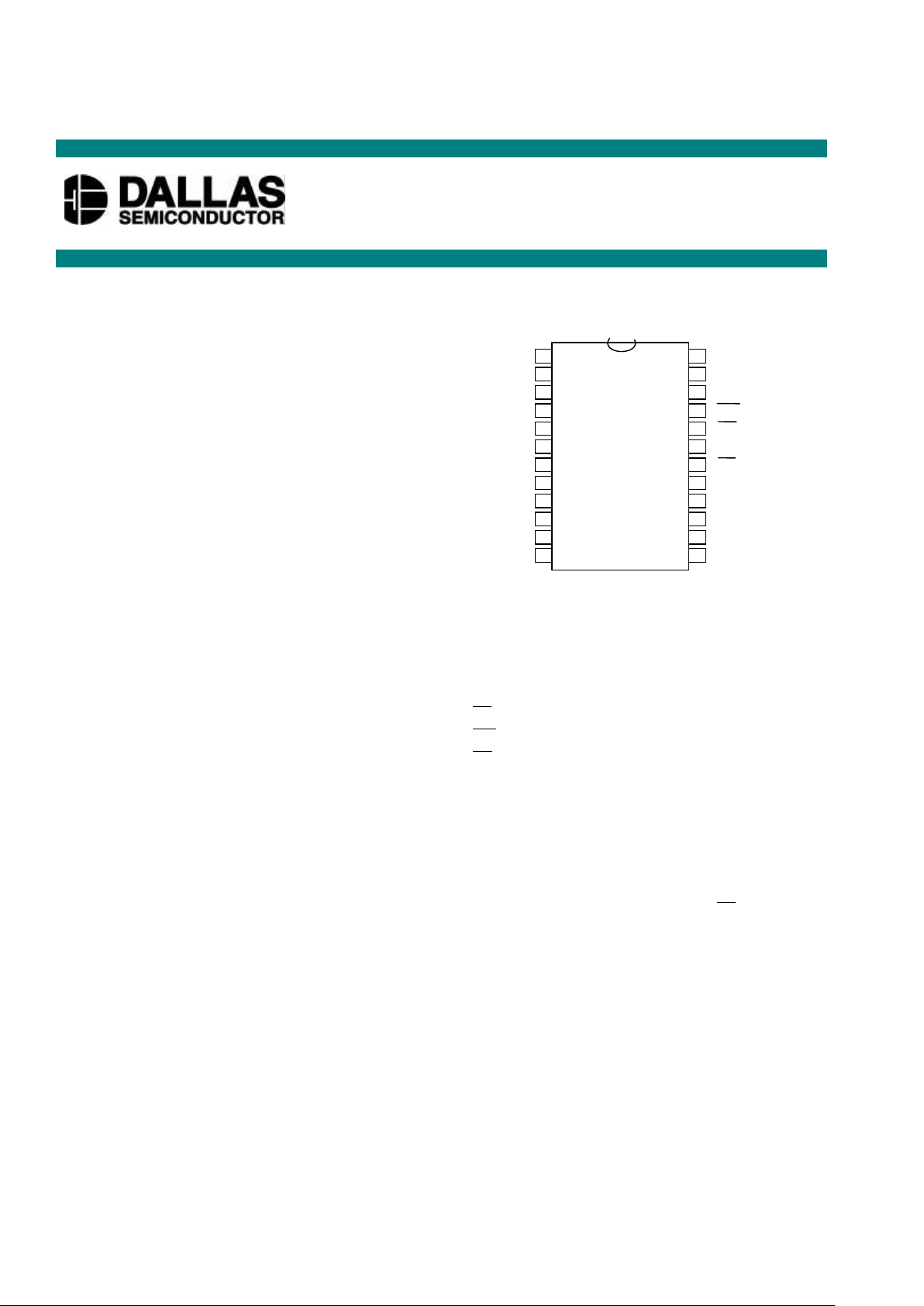
PIN ASSIGNMENT
PIN DESCRIPTION
A0 - A10 - Address Inputs
DQ0 - DQ7 - Data Input/Output
CE - Chip Enable Input
WE - Write Enable Input
OE - Output Enable Input
V
CC
- Power Supply Input 2.7V - 5.5V
GND - Ground
DESCRIPTION
The DS2016 2k x 8 3V/5V Operation Static RAM is a 16,384-bit, low-power, fully static random access
memory organized as 2048 words by 8 bits using CMOS technology. The device operates from a single
power supply with a voltage input between 2.7 and 5.5 volts. The chip enable input (CE ) is used for
device selection and can be used in order to achieve the minimum standby current mode, which facilitates
both battery operated and battery backup applications. The device provides access times as fast as 100 ns
when operated from a 5-volt power supply input and also provides relatively good performance of 250 ns
access while operating from a 3-volt input. The device maintains TTL-level inputs and outputs over the
input voltage range of 2.7 to 5.5 volts. The DS2016 is most suitable for low-power applications where
battery operation or battery backup for nonvolatility is required. The DS2016 is a JEDEC-standard 2k x 8
SRAM and is pin-compatible with ROM and EPROM of similar density.
DS2016
2k x 8 3V/5V Operation Static RAM
www.dalsemi.com
123456789101112132423222120191817161514VCCA8A9WEOEA10CEDQ7
DQ6
DQ5
DQ4
DQ3
A7A6A5A4A3A2A1A0DQ0
DQ1
DQ2
GND
DS2016 24-Pin DIP (600-mil)
DS2016R 24-Pin SOIC (300-mil)
Page 2
DS2016
2 of 9
OPERATION MODE
MODE
CE
OE WE
A0-A10 DQ-DQ7 POWER
READ L L H STABLE DATA OUT I
CCO
WRITE L X L STABLE DATA IN I
CCO
DESELECT L H H X HIGH-Z I
CCO
STANDBY H X X X HIGH-Z I
CCS
ABSOLUTE MAXIMUM RATINGS
SYMBOL PARAMETER RATING
V
CC
Power Supply Voltage -0.3V to +7.0V
V
IN
, V
I/O
Input, Input/Output Voltage -0.3 to VCC +0.3V
T
STG
Storage Temperature -55°C to +125°C
T
OPR
Operating Temperature -40°C to +85°C
T
SOLDER
Soldering Temperature/Time 260 °C for 10 seconds
CAPACITANCE (TA= 25°C)
PARAMETER SYMBOL MIN TYP MAX UNITS NOTES
Input Capacitance C
IN
5 10 pF
Input/Output Capacitance C
I/O
5 12 pF
+5-VOLT OPERATION
RECOMMENDED DC OPERATING CONDITIONS (TA= -40°C to +85°C)
PARAMETER SYMBOL MIN TYP MAX UNITS NOTES
Power Supply Voltage V
CC
4.5 5.0 5.5 V
Input High Voltage V
IH
2.0 VCC+0.3 V
Input Low Voltage V
IL
-0.3 0.8 V
Data Retention Voltage V
DR
2.0 5.5 V
DC CHARACTERISTICS (TA= -40°C to +85°C; VCC = 5V ±10%)
PARAMETER SYMBOL CONDITIONS MIN TYP MAX UNITS
Input Leakage Current I
IL
0V ≤ VIN ≤ V
CC
±
0.1 µA
I/O Leakage Current I
LO
CE = V
IH
, 0V ≤ VIO ≤ V
CC
±
0.5 µA
Output High Current I
OH
VOH = 2.4V -1.0 mA
Output Low Current I
OL
VOL = 0.4V 4.0 mA
Standby Current I
CCS1
CE = 2.0V
0.3 mA
Standby Current I
CCS2
CE ≥ V
CC
-0.5V tA =60°C
1 µA
Standby Current I
CCS2
CE ≥ V
CC
-0.5V tA =25°C
100 nA
Operating Current I
CCO
CE = 0.8V, 200 ns cycle
55 mA
Page 3
DS2016
3 of 9
AC CHARACTERISTICS READ CYCLE (TA= -40°C to +85°C; VCC = 5V ±10%)
DS2016-100 DS2016-150
PARAMETER SYMBOL
MIN TYP MAX MIN TYP MAX
UNITS NOTES
Read Cycle Time t
RC
100 150 ns
Access Time t
ACC
100 150 ns
OE to Output Valid
t
OE
50 70 ns
CE to Output Valid
t
CO
100 150 ns
CE or OE to Output
Active
t
COE
5 5 ns
Output High-Z from
Deselection
t
OD
5 35 10 60 ns
Output Hold from
Address Change
t
OH
5 10 ns
AC CHARACTERISTICS WRITE CYCLE (TA= -40°C to +85°C; VCC = 5V±10%)
DS2016-100 DS2016-150
PARAMETER SYMBOL
MIN TYP MAX MIN TYP MAX
UNITS NOTES
Write Cycle Time t
WC
100 150 ns
Write Pulse Width t
WP
75 120 ns
Address Setup Time t
AW
0 0 ns
Write Recovery
Time
t
WR
10 10 ns
Output High-Z from
WE
t
ODW
35 70 ns
Output Active from
WE
t
OEW
5 5 ns
Data Setup Time t
DS
40 60 ns
Data Hold Time t
DH
0 0 ns
DATA RETENTION CHARACTERISTICS (TA = -40°C to +85°C)
PARAMETER SYMBOL CONDITIONS MIN TYP MAX UNITS
Data Retention Supply
Voltage
V
DR
CE ≥ V
CC
- 0.5V
2.0 5.5 V
Data Retention
Current at 5.5V
I
CCR1
CE ≥ V
CC
- 0.5V
0.1* 1 µA
Data Retention
Current at 2.0V
I
CCR2
CE ≥ V
CC
- 0.5V
50* 750 nA
Chip Deselect to Data
Retention
t
CDR
0 µs
Recovery Time t
R
2 ms
* Typical values are at 25°C
Page 4

DS2016
4 of 9
+3-VOLT OPERATION
RECOMMENDED DC OPERATING CONDITIONS (TA = -40°C to +85°C)
PARAMETER SYMBOL MIN TYP MAX UNITS NOTES
Power Supply Voltage V
CC
2.7 3.0 3.5 V
Input High Voltage V
IH
2.0 VCC + 0.3 V
Input Low Voltage V
IL
-0.3 0.6 V
Data Retention Voltage V
DR
2.0 3.5 V
DC CHARACTERISTICS (TA = -40°C to +85°C; VCC = 2.7V to 3.5V)
PARAMETER SYMBOL CONDITIONS MIN TYP MAX UNITS
Input Leakage Current I
IL
0V ≤ VIN ≤ V
CC
±0.1 µA
I/O Leakage Current I
LO
CE =V
IH
, 0V≤VIO≤V
CC
±0.5 µA
Output High Current I
OH
VOH = 2.2V -0.5 mA
Output Low Current I
OL
VOL = 0.4V 4.0 mA
Standby Current I
CCS1
CE = 2.0V
0.1 mA
Standby Current I
CCS2
CE ≥V
CC
-0.3V TA=60°C
500 nA
Standby Current I
CCS2
CE ≥V
CC
-0.3V TA=25°C
50 nA
Operating Current I
CCO
CE =0.6V min cycle
25 mA
AC CHARACTERISTICS READ CYCLE
(TA = -40°C to +85°C; VCC = 2.7V to 3.5V)
PARAMETER SYMBOL MIN TYP MAX UNITS NOTES
Read Cycle Time t
RC
250 ns
Access Time t
ACC
250 ns
OE to Output Valid
t
OE
120 ns
CE to Output Valid
t
CO
250 ns
CE or OE to Output Active
t
COE
15 ns
Output High-Z
from Deselection
t
OD
5 100 ns
Output Hold from
Address Change
t
OH
15 ns
Page 5

DS2016
5 of 9
AC CHARACTERISTICS WRITE CYCLE
(TA = -40°C to +85°C; VCC = 2.7V to 3.5V)
PARAMETER SYMBOL MIN TYP MAX UNITS NOTES
Write Cycle Time t
WC
250 ns
Write Pulse Width t
WP
190 ns
Address Setup Time t
AW
0 ns
Write Recovery Time t
WR
25 ns
Output High-Z from WE
t
ODW
90 ns
Output Active from WE
t
OEW
5 ns
Data Setup Time t
DS
100 ns
Data Hold Time t
DH
0 ns
DATA RETENTION CHARACTERISTICS (TA = -40°C to +85°C)
PARAMETER SYMBOL CONDITIONS MIN TYP MAX UNITS
Data Retention
Supply Voltage
V
DR
CE ≥ V
CC
- 0.3V
2.0 3.5 V
Data Retention
Current at 3.5V
I
CCR1
CE ≥ V
CC
- 0.3V
50* 1000 nA
Data Retention
Current at 2.0V
I
CCR2
CE ≥ V
CC
- 0.3V
50* 750 nA
Chip Deselect to
Data Retention
t
CDR
0 µs
Recovery Time t
R
2 ms
* Typical values are at 25°C
TIMING DIAGRAM: READ CYCLE
SEE NOTE 1
Page 6

DS2016
6 of 9
TIMING DIAGRAM: WRITE CYCLE 1
SEE NOTES 2, 3, 4, 5, 6 AND 7
TIMING DIAGRAM: WRITE CYCLE 2
SEE NOTES 2, 3, 4, 5, 6 AND 7
Page 7

DS2016
7 of 9
TIMING DIAGRAM: DATA RETENTION - POWER-UP, POWER-DOWN Figure 1
SEE NOTE 8
NOTES:
1. WE is high for read cycles.
2. OE = VIH or VIL. If OE = VIH during write cycle, the output buffers remain in a high impedance
state.
3. tWP is specified as the logical AND of CE and WE . tWP is measured from the latter of CE or WE
going low to the earlier of CE or WE going high.
4. tDH and tDS are measured from the earlier of CE or WE going high.
5. If the CE low transition occurs simultaneously with or later than the WE low transition, the
output buffers remain in a high impedance state.
6. If the CE high transition occurs prior to or simultaneously with the WE high transition, the output
buffers remain in a high impedance state.
7. If WE is low or the WE low transition occurs prior to or simultaneously with the CE low
transition, the output buffers remain in a high impedance state.
8. If the VIH level of CE is 2.0V during the period that VCC voltage is going down from 4.5V to
2.7V, I
CCS1
current flows.
9. The DS2016 maintains full operation from 5.5V to 2.7V. The electrical characteristics tables show
two tested and guaranteed points of operation. For operation between 4.5V and 3.5 volts, use the
composite worst case characteristics from both 5V and 3V operation for design purposes.
DC TEST CONDITIONS
Outputs Open
All voltages are referenced to ground.
AC TEST CONDITIONS
Output Load: 100 pF + 1TTL Gate
Input Pulse Levels: 0V - 3.0V
Timing Measurement Reference Levels
Input: 1.5V
Output: 1.5V
Input Pulse Rise and Fall Times: 5 ns
Page 8

DS2016
8 of 9
DS2016 24-PIN DIP
PKG 24-PIN
DIM MIN MAX
A IN.
MM
1.245
31.62
1.270
32.25
B IN.
MM
0.530
13.46
0.550
13.97
C IN.
MM
0.140
3.56
0.160
4.06
D IN.
MM
0.600
15.24
0.625
15.88
E IN.
MM
0.015
0.380
0.050
1.27
F IN.
MM
0.120
3.05
0.145
3.68
G IN.
MM
0.090
2.29
0.110
2.79
H IN.
MM
0.625
15.88
0.675
17.15
J IN.
MM
0.008
0.20
0.012
0.30
K IN.
MM
0.015
0.38
0.022
0.56
Page 9

DS2016
9 of 9
DS2016S 24-PIN SOIC
PKG 24-PIN
DIM MIN MAX
A IN.
MM
0.094
2.38
0.105
2.68
A1 IN.
MM
0.004
0.102
0.012
0.30
b IN.
MM
0.013
0.33
0.020
0.51
C IN.
MM
0.009
0.229
0.013
0.33
D IN.
MM
0.598
15.19
0.612
15.54
e IN.
MM
0.050 BSC
1.27 BSC
E1 IN.
MM
0.290
7.37
0.300
7.62
H IN.
MM
0.398
10.11
0.416
10.57
L IN.
MM
0.016
0.40
0.040
1.02
α
0° 8°
The chamfer on the body is optional. If it is not present, a
terminal 1 identifier must be positioned so that ½ or more of its
area is contained in the hatched zone.
 Loading...