

Page 1
DS2007SF
DS2007SF
Rectifier Diode
Replaces September 2001 version, DS4189-4.0 DS4189-4.1 December 2001
FEATURES
■ Double Side Cooling
■ High Surge Capability
APPLICATIONS
■ Rectification
■ Freewheel Diode
■ DC Motor Control
■ Power Supplies
■ Welding
■ Battery Chargers
VOLTAGE RATINGS
Type Number Repetitive Peak
Reverse Voltage
V
RRM
V
DS2007SF40
DS2007SF39
DS2007SF38
DS2007SF37
DS2007SF36
DS2007SF35
Lower voltage grades available.
4000
3900
3800
3700
3600
3500
Conditions
= V
V
RSM
RRM
+ 100V
KEY PARAMETERS
V
4000V
RRM
I
1594A
F(AV)
I
25000A
FSM
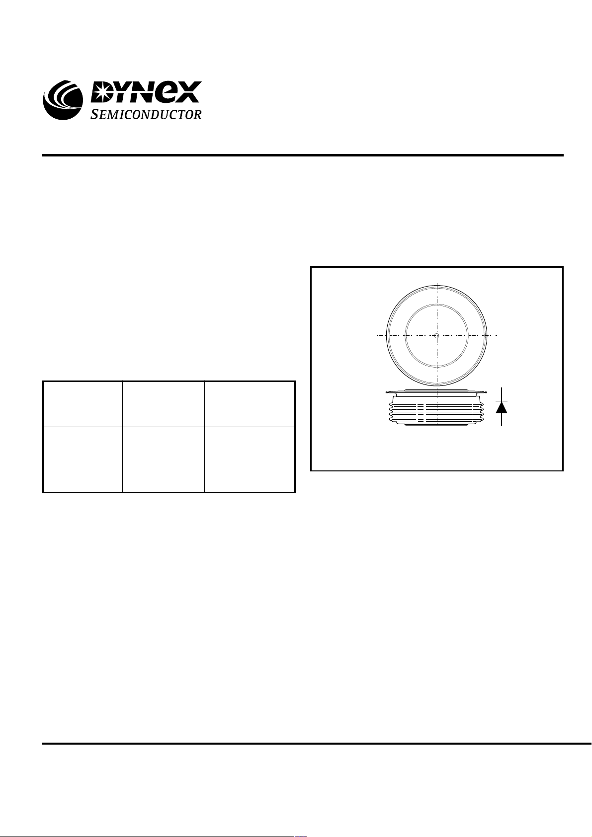
Outline type code: F
See Package Details for further information.
Fig. 1 Package outline
ORDERING INFORMATION
When ordering, select the required part number shown in the
Voltage Ratings selection table, e.g.:
DS2007SF36
Note: Please use the complete part number when ordering
and quote this number in any future correspondance relating
to your order.
www.dynexsemi.com
1/7
Page 2
DS2007SF
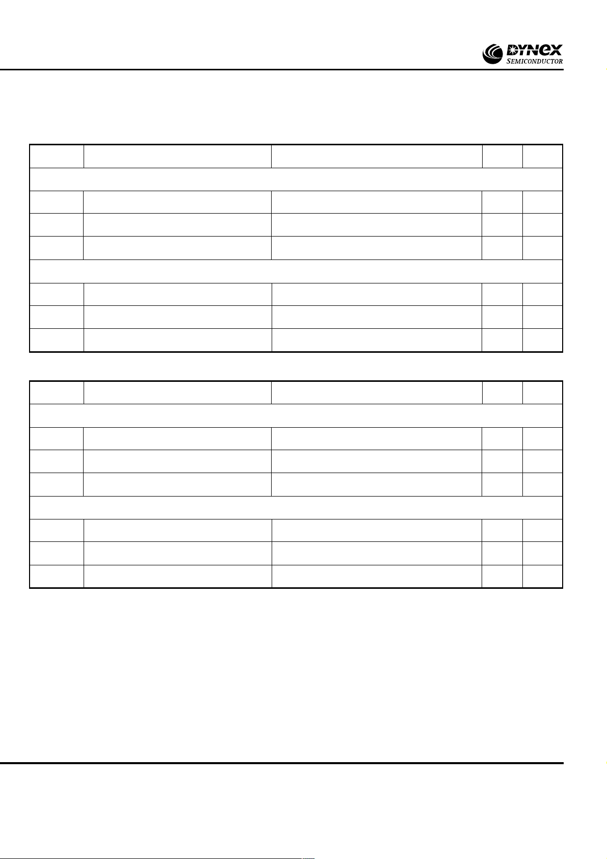
CURRENT RATINGS
T
= 75oC unless otherwise stated
case
Symbol Parameter Conditions
Double Side Cooled
I
F(AV)
I
F(RMS)
I
Mean forward current
RMS value
F
Continuous (direct) forward current
Half wave resistive load 1594 A
Single Side Cooled (Anode side)
I
F(AV)
I
F(RMS)
I
F
T
= 100oC unless otherwise stated
case
Mean forward current
RMS value
Continuous (direct) forward current
Half wave resistive load 1144 A
Symbol Parameter Conditions
Double Side Cooled
I
F(AV)
Mean forward current
Half wave resistive load 1225 A
UnitsMax.
- 2504 A
- 2295 A
- 1797 A
- 1553 A
UnitsMax.
I
F(RMS)
I
F
RMS value
Continuous (direct) forward current
Single Side Cooled (Anode side)
I
F(AV)
I
F(RMS)
I
F
Mean forward current
RMS value
Continuous (direct) forward current
- 1923 A
- 1720 A
Half wave resistive load 820 A
- 1287 A
- 1050 A
2/7
www.dynexsemi.com
Page 3
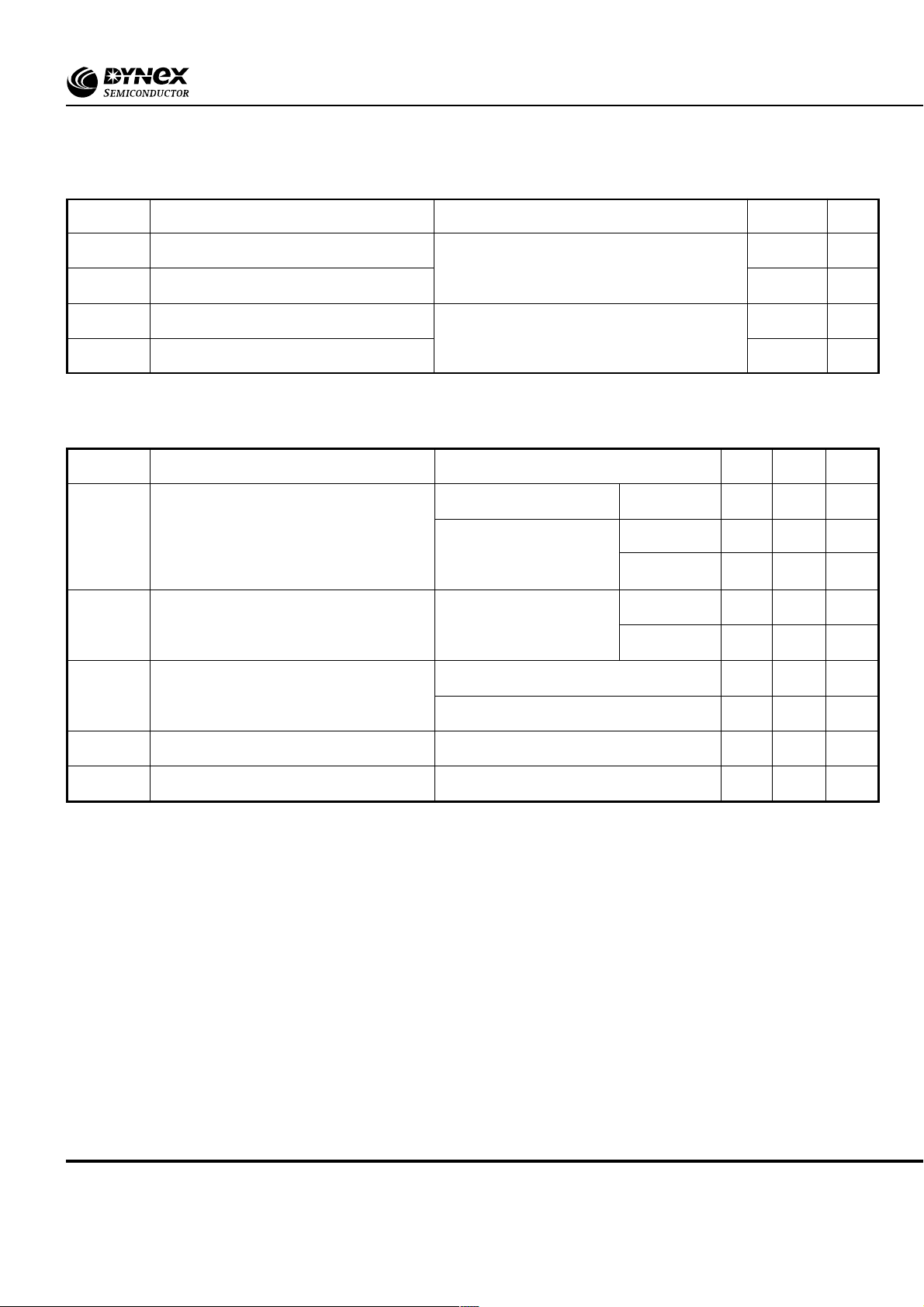
SURGE RATINGS
DS2007SF
I
FSM
2
tI
I
I
FSM
I2t
Surge (non-repetitive) forward current
2
t for fusing
Surge (non-repetitive) forward current
2
I
t for fusing A2s
THERMAL AND MECHANICAL DATA
Symbol
R
th(j-c)
R
th(c-h)
Thermal resistance - junction to case
Thermal resistance - case to heatsink
Parameter
Conditions
10ms half sine; T
VR = 50% V
10ms half sine; T
VR = 0
Conditions Min. Max. Units
Double side cooled
Single side cooled
Clamping force 19.5kN
with mounting compound
case
- 1/4 sine
RRM
case
= 150oC
= 150oC
dc
Cathode dc
Double side
Single side
Max. UnitsSymbol Parameter
20.0 kA
6
2.0 x 10
A2s
25.0 kA
3.125 x 10
6
- 0.022oC/W
o
C/W- 0.038Anode dc
o
- 0.052
0.004
-
C/W
o
C/W
- 0.008oC/W
Forward (conducting) - 160
T
vj
T
stg
- kN22.018.0
Virtual junction temperature
Storage temperature range
Clamping force
-
150
-55 175
o
C
o
CReverse (blocking)
o
C
www.dynexsemi.com
3/7
Page 4
DS2007SF
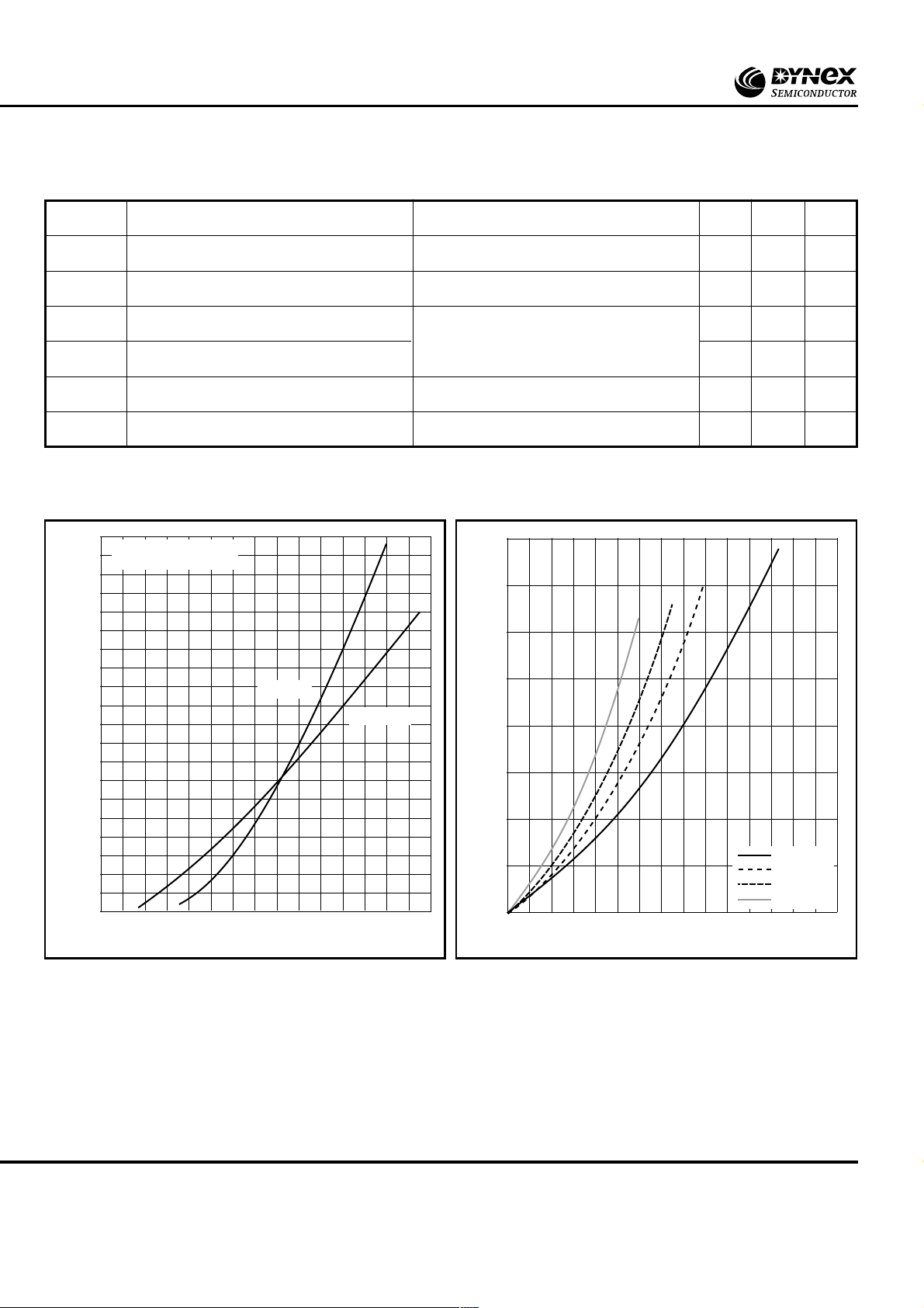
CHARACTERISTICS
Symbol
V
FM
I
RRM
Q
S
I
RR
V
TO
r
T
CURVES
5000
4000
- (A)
F
Parameter
Forward voltage
Peak reverse current
Total stored charge
Peak recovery current
Threshold voltage
Slope resistance 0.29 mΩ
Measured under pulse
conditions
At V
, T
RRM
IF = 2000A, dIRR/dt = 3A/µs,
T
= 150˚C, VR = 100V
case
= 150˚C - 0.82 V
At T
vj
At Tvj = 150˚C -
Conditions Min. Max. Units
= 25oC
case
= 150oC-75mA
case
- 1.6 VAt 3400A peak, T
-
- 110 A
4000
3000
µC3500
3000
2000
Instantaneous forward current, I
1000
0
0.5 1.0 1.5 2.0
Instantaneous forward voltage, V
Fig.2 Maximum (limit) forward characteristics
VFM Equation:V
= A + Bln (IF) + C.IF+D.√I
FM
F
Tj = 25˚C
Tj = 150˚C
- (V)
F
2000
Mean power dissipation - (W)
1000
0
0 1000 2000 3000
Mean forward current, I
F(AV)
- (A)
Fig.3 Dissipation curves
Where A = 0.658789
B = –0.01706
C = 0.000194
D = 0.010358
these values are valid for T
= 125˚C for IF 500A to 5000A
j
dc
Half wave
3 phase
6 phase
4/7
www.dynexsemi.com
Page 5
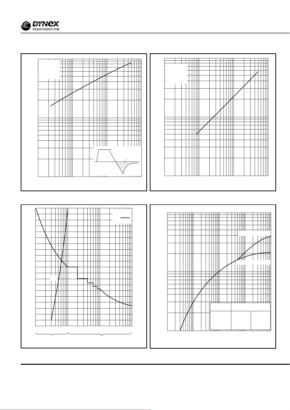
DS2007SF
10000
Conditions:
T
= 150˚C
j
= 100V
V
R
I
= 2000A
F
- (µC)
S
1000
Stored charge, Q
I
F
dIF/dt
100
0.1 1.0 10 100
Rate of decay of on-state current, dI
/dt - (A/µs)
F
Fig.4 Total stored charge Fig.5 Maximum reverse recovery current
1000
Conditions:
T
= 150˚C
j
V
= 100V
R
= 2000A
I
F
- (A)
rr
100
Reverse recovery current I
Q
S
I
RM
10
0.1 1.0 10 100
Rate of decay of forward current, dI
/dt - (A/µs)
F
40
I2t = I2 x t
2.0
^
2
30
I
2
t value - (A
20
I2t
10
Peak half sine forward current - (kA)
0
1.5
1.0
2
s x 10
6
)
1101235102050
ms Cycles at 50Hz
Duration
0.1
Anode side cooled
Double side cooled
0.01
Effective thermal resistance
Junction to case ˚C/W
Double side
d.c.
0.022
0.024
0.026
0.027
Single side
0.038
0.040
0.042
0.043
Thermal Impedance - junction to case - (˚C/W)
0.001
Conduction
Halfwave
3 phase 120˚
6 phase 60˚
0.001 0.01 0.1 1.0 10
Time - (s)
Fig.6 Surge (non-repetitive) forward current vs time
(with 50% V
RRM
at T
case
150˚C)
www.dynexsemi.com
Fig.7 Maximum (limit) transient thermal impedance -
junction to case
5/7
Page 6
DS2007SF
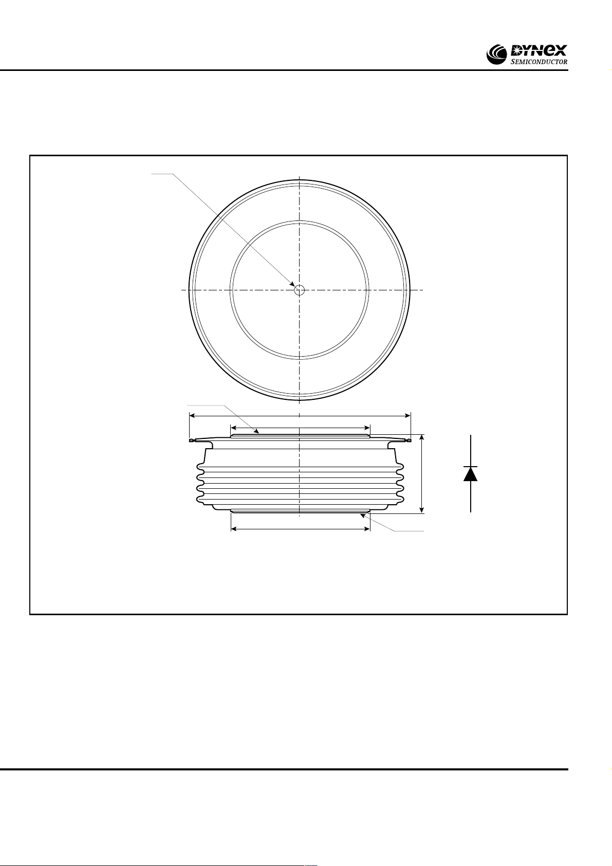
PACKAGE DETAILS
For further package information, please contact your nearest Customer Service Centre. All dimensions in mm, unless stated otherwise.
DO NOT SCALE.
Hole Ø3.6x2.0 deep (in both electrodes)
Cathode
Note:
1. Package maybe supplied with pins and/or tags.
Ø76 max
Ø48 nom
Ø48 nom
Nominal weight: 450g
Clamping force: 19.6kN ± 10%
Package outline type code: F
Anode
27.0
25.4
6/7
www.dynexsemi.com
Page 7
DS2007SF
POWER ASSEMBLY CAPABILITY
The Power Assembly group was set up to provide a support service for those customers requiring more than the basic semiconductor,
and has developed a flexible range of heatsink / clamping systems in line with advances in device types and the voltage and current
capability of our semiconductors.
We offer an extensive range of air and liquid cooled assemblies covering the full range of circuit designs in general use today. The
Assembly group continues to offer high quality engineering support dedicated to designing new units to satisfy the growing needs of our
customers.
Using the up to date CAD methods our team of design and applications engineers aim to provide the Power Assembly Complete solution
(PACs).
DEVICE CLAMPS
Disc devices require the correct clamping force to ensure their safe operation. The PACs range offers a varied selection of pre-loaded
clamps to suit all of our manufactured devices. This include cube clamps for single side cooling of ‘T’ 22mm
Clamps are available for single or double side cooling, with high insulation versions for high voltage assemblies.
Please refer to our application note on device clamping, AN4839
HEATSINKS
Power Assembly has its own proprietary range of extruded aluminium heatsinks. They have been designed to optimise the performance
or our semiconductors. Data with respect to air natural, forced air and liquid cooling (with flow rates) is available on request.
For further information on device clamps, heatsinks and assemblies, please contact your nearest Sales Representative or Customer
Services.
http://www.dynexsemi.com
e-mail: [email protected]
HEADQUARTERS OPERATIONS
DYNEX SEMICONDUCTOR LTD
Doddington Road, Lincoln.
Lincolnshire. LN6 3LF. United Kingdom.
Tel: 00-44-(0)1522-500500
Fax: 00-44-(0)1522-500550
DYNEX POWER INC.
99 Bank Street, Suite 410,
Ottawa, Ontario, Canada, K1P 6B9
Tel: 613.723.7035
Fax: 613.723.1518
Toll Free: 1.888.33.DYNEX (39639)
Datasheet Annotations:
Dynex Semiconductor annotate datasheets in the top right hard corner of the front page, to indicate product status. The annotations are as follows:-
Target Information: This is the most tentative form of information and represents a very preliminary specification. No actual design work on the product has been started.
Preliminary Information: The product is in design and development. The datasheet represents the product as it is understood but details may change.
Advance Information: The product design is complete and final characterisation for volume production is well in hand.
No Annotation: The product parameters are fixed and the product is available to datasheet specification.
This publication is issued to provide information only which (unless agreed by the Company in writing) may not be used, applied or reproduced for any purpose nor form part of any order or contract nor to be regarded as
a representation relating to the products or services concerned. No warranty or guarantee express or implied is made regarding the capability, performance or suitability of any product or service. The Company reserves
the right to alter without prior notice the specification, design or price of any product or service. Information concerning possible methods of use is provided as a guide only and does not constitute any guarantee that such
methods of use will be satisfactory in a specific piece of equipment. It is the user's responsibility to fully determine the performance and suitability of any equipment using such information and to ensure that any publication
or data used is up to date and has not been superseded. These products are not suitable for use in any medical products whose failure to perform may result in significant injury
or death to the user. All products and materials are sold and services provided subject to the Company's conditions of sale, which are available on request.
All brand names and product names used in this publication are trademarks, registered trademarks or trade names of their respective owners.
CUSTOMER SERVICE CENTRES
Mainland Europe Tel: +33 (0)1 58 04 91 00. Fax: +33 (0)1 46 38 51 33
North America Tel: (613) 723-7035. Fax: (613) 723-1518.
UK, Scandinavia & Rest Of World Tel: +44 (0)1522 500500. Fax: +44 (0)1522 500020
SALES OFFICES
Mainland Europe Tel: +33 (0)1 58 04 91 00. Fax: +33 (0)1 46 38 51 33
North America Tel: (613) 723-7035. Fax: (613) 723-1518. Toll Free: 1.888.33.DYNEX (39639) /
Tel: (949) 733-3005. Fax: (949) 733-2986.
UK, Scandinavia & Rest Of World Tel: +44 (0)1522 500500. Fax: +44 (0)1522 500020
These offices are supported by Representatives and Distributors in many countries world-wide.
© Dynex Semiconductor 2001 Publication No. DS4189-4 Issue No. 4.1 December 2001
TECHNICAL DOCUMENTATION – NOT FOR RESALE. PRINTED IN UNITED KINGDOM
www.dynexsemi.com
7/7
 Loading...