

Page 1
AD0AD1AD2AD3A
A
R
IRQKSR
W
P
C
R
I
K
R
WR P
A
A
A
A
A
A
A
A
A
C
R
I
K
R
WRPWR
A
A
AD2AD3A
A
A
A
A
C
19-5215; Rev 4/10
www.maxim-ic.com
FEATURES
Incorporates Industry-Standard DS1287 PC Clock
plus Enhanced Features Such as: Y2K Compliant
+3V or +5V Operation
64-Bit Silicon Serial Number
Power-Control Circuitry Supports System
Power-On from Date/Time Alarm or Key
Closure
32kHz Output for Power Management
Crystal-Select Bit Allows RTC to Operate with
6pF or 12.5pF Crystal
SMI Recovery Stack
242 Bytes Battery-Backed NV RAM
Auxiliary Battery Input
APPLICATIONS
Embedded Systems
Utility Meters
Security Systems
Network Hubs, Bridges, and Routers
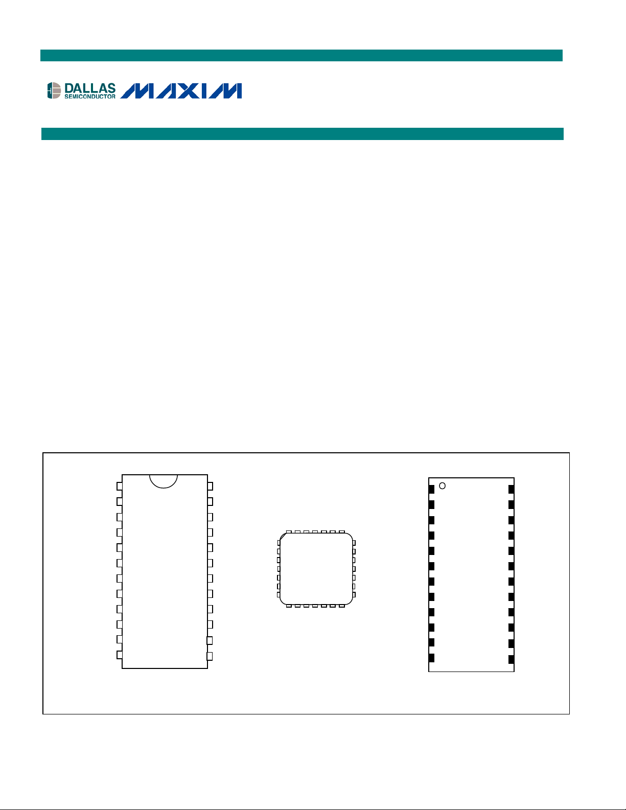
PIN CONFIGURATIONS
TOP VIEW
DS1685/DS1687
3V/5V Real-Time Clocks
RAM Clear Input
Century Register
Date Alarm Register
Compatible with Existing BIOS for Original
DS1287 Functions
Available as Chip (DS1685) or Stand-Alone
Encapsulated DIP (EDIP) with Embedded
Battery and Crystal (DS1687)
Timekeeping Algorithm Includes Leap-Year
Compensation Valid Through 2099
Underwriters Laboratory (UL) Recognized
WR
X1
X2
D0
D1
D2
D3
D4
D5
D6
D7
GND
1
2
DS1685/
3
DS1685S/
DS1685E
4
5
6
7
8
9
10
11
12
PDIP (0.600
SO (0.300)/
TSSOP (0.173)
24
23
22
21
20
19
18
17
16
15
14
13
)/
V
CC
SQW
V
BAUX
CLR
V
BAT
RQ
S
D
GND
LE
S
1
D0
D1
D4
D5
D6
D7
2
3
4
5
6
7
8
9
10
11
12
DS1687
CC
D4
D5
N.C.
WR
X1
X2
4 3 2 1 28 27 26
5
6
DS1685Q
7
8
9
10
11
12 13 14 15 16 17 18
AD6
V
N.C.
S
N.C.
AD7
GND
VBAUX
SQW
25
CLR
24
V
BAT
23
22
21
D
20
GND
19
R
N.C.
ALE
N.C.
N.C.
PLCC
GND
24
23
22
21
20
19
18
17
16
15
14
13
V
CC
SQW
V
BAUX
CLR
N.C.
RQ
S
D
N.C.
LE
S
EDIP (0.740)
1 of 34
Page 2
DS1685/DS1687 3V/5V Real-Time Clocks
ORDERING INFORMATION
PART* TEMP RANGE
DS1685-3+ 0°C to +70°C 3 24 PDIP (0.600”) DS1685-3
DS1685-5+ 0°C to +70°C 5 24 PDIP (0.600”) DS1685-5
DS1685-5IND+ -40°C to +85°C 5 24 PDIP (0.600”) DS1685-5
DS1685E-3+ 0°C to +70°C 3 24 TSSOP (0.173”) DS1685E-3
DS1685E-5+ 0°C to +70°C 5 24 TSSOP (0.173”) DS1685E
DS1685EN-3+ -40°C to +85°C 3 24 TSSOP (0.173”) DS1685E-3
DS1685EN-5+ -40°C to +85°C 5 24 TSSOP (0.173”) DS1685E
DS1685E-3+T&R 0°C to +70°C 3 24 TSSOP (0.173”)/Tape & Reel DS1685E-3
DS1685E-5+T&R 0°C to +70°C 5 24 TSSOP (0.173”)/Tape & Reel DS1685E
DS1685EN-3+T&R -40°C to +85°C 3 24 TSSOP (0.173”)/Tape & Reel DS1685E-3
DS1685EN-5+T&R -40°C to +85°C 5 24 TSSOP (0.173”) /T&R DS1685E
DS1685Q-3+ 0°C to +70°C 3 28 PLCC DS1685Q-3
DS1685Q-5+ 0°C to +70°C 5 28 PLCC DS1685Q-5
DS1685QN-3+ -40°C to +85°C 3 28 PLCC DS1685Q-3
DS1685QN-5+ -40°C to +85°C 5 28 PLCC DS1685Q-5
DS1685Q-3+T&R 0°C to +70°C 3 28 PLCC/Tape & Reel DS1685Q-3
DS1685Q-5+T&R 0°C to +70°C 5 28 PLCC/Tape & Reel DS1685Q-5
DS1685S-3+ 0°C to +70°C 3 24 SO (0.300”) DS1685S-3
DS1685S-5+ 0°C to +70°C 5 24 SO (0.300”) DS1685S-5
DS1685S-3+T&R 0°C to +70°C 3 24 SO (0.300”)/Tape & Reel DS1685S-3
DS1685S-5+T&R 0°C to +70°C 5 24 SO (0.300”)/Tape & Reel DS1685S-5
DS1687-3+ 0°C to +70°C 3 24 EDIP (0.740”) DS1687-3
DS1687-5+ 0°C to +70°C 5 24 EDIP (0.740”) DS1687-5
DS1687-3IND+ -40°C to +85°C 3 24 EDIP (0.740”) DS1687-3
DS1687-5IND+ -40°C to +85°C 5 24 EDIP (0.740”) DS1687-5
VOLTAGE
(V)
PIN-PACKAGE TOP MARK*
+Denotes a lead(Pb)-free/RoHS-compliant device. A “+” anywhere on the top mark indicates a lead-free/RoHS-compliant device.
*An “N” or “IND” denotes an industrial temperature grade device.
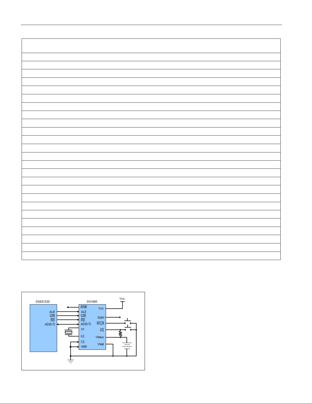
TYPICAL OPERATING CIRCUIT
2 of 34
Page 3

DS1685/DS1687 3V/5V Real-Time Clocks
DETAILED DESCRIPTION
The DS1685/DS1687 are real-time clocks (RTC) designed as successors to the industry-standard DS1285,
DS1385, DS1485, and DS1585 PC RTCs. These devices provide the industry-standard DS1285 clock function with
either +3.0V or +5.0V operation. The DS1685 also incorporates a number of enhanced features including a silicon
serial number, power-on/off control circuitry, 242 bytes of user NV SRAM, and 32.768kHz output for sustaining
power management activities.
The DS1685/DS1687 power-control circuitry allows the system to be powered on by an external stimulus such as a
keyboard or by a time and date (wake-up) alarm. The PWR output pin can be triggered by one or either of these
events, and can be used to turn on an external power supply. The PWR pin is under software control, so that when
a task is complete, the system power can then be shut down.
The DS1685 is a clock/calendar chip with the features described above. An external crystal and battery are the
only components required to maintain time-of-day and memory status in the absence of power. The DS1687
incorporates the DS1685 chip, a 32.768kHz crystal, and a lithium battery in a complete, self-contained timekeeping
EDIP. The entire unit is fully tested at Maxim such that a minimum of 10 years of timekeeping and data retention in
the absence of V
is guaranteed.
CC
OPERATION
The block diagram in Figure 1 shows the pin connections with the major internal functions of the DS1685/DS1687.
The following paragraphs describe the function of each pin.
3 of 34
Page 4

PIN DESCRIPTIONS
PIN
DS1685 DS1687
PDIP,
SO,
TSSOP
1 2 1
—
2 3 — X1
3 4 — X2
4–11
12, 16 15, 20 12 GND
PLCC EDIP
1, 11, 13,
18
5–10, 12,
14
2, 3, 16,
20
4–11 AD0–AD7
NAME FUNCTION
PWR
N.C.
DS1685/DS1687 3V/5V Real-Time Clocks
Active Low Power-On Output, Open Drain. The PWR pin is intended for use
as an on/off control for the system power. With V
the DS1685/DS1687, PWR can be automatically activated from a kickstart
input by the KS pin or from a wake-up interrupt. Once the system is
powered on, the state of PWR can be controlled by bits in the Maxim
registers. The PWR pin can be connected through a pullup resistor to a
positive supply. The voltage of the pullup supply should be no greater than
5.5V.
No Connection. Pins missing by design.
Connections for Standard 32.768kHz Quartz Crystal. For greatest
accuracy, the DS1685 must be used with a crystal that has a specified load
capacitance of either 6pF or 12.5pF. The crystal-select (CS) bit in Extended
Control Register 4B is used to select operation with a 6pF or 12.5pF
crystal. The crystal is attached directly to the X1 and X2 pins. There is no
need for external capacitors or resistors. Note: X1 and X2 are very highimpedance nodes. It is recommended that they and the crystal be guardringed with ground and that high-frequency signals be kept away from the
crystal area.
Multiplexed, Bidirectional Address/Data Bus. The addresses are present
during the first portion of the bus cycle and the same pins and signal paths
are used for data in the second portion of the cycle. Address/data
multiplexing does not slow the access time of the DS1685 since the bus
change from address to data occurs during the internal RAM access time.
Addresses must be valid prior to the latter portion of ALE, at which time the
DS1685/DS1687 latches the address. Valid write data must be present and
held stable during the latter portion of the WR pulse. In a read cycle, the
DS1685/DS1687 outputs 8 bits of data during the latter portion of the RD
pulse. The read cycle is terminated and the bus returns to a highimpedance state as RD transitions high. The address/data bus also serves
as a bidirectional data path for the extended RAM.
Ground
voltage removed from
CC
Chip-Select Input, Active-Low. The chip-select signal must be asserted low
during a bus cycle for the RTC portion of the DS1685/DS1687 to be
13 16 13
14 17 14 ALE
15 19 15
17 21 17
CS
WR
RD
accessed. CS must be kept in the active state during RD and WR timing.
Bus cycles that take place with ALE asserted but without asserting CS will
latch addresses. However, no data transfer will occur.
Address-Strobe Input, Active High. A pulse on the address strobe pin
serves to demultiplex the bus. The falling edge of ALE causes the RTC
address to be latched within the DS1685/DS1687.
Write Input, Active Low. The WR signal is an active-low signal. The WR
signal defines the time period during which data is written to the addressed
register.
Read Input, Active Low. RD identifies the time period when the
DS1685/DS1687 drives the bus with RTC read data. The RD signal is an
enable signal for the output buffers of the clock.
4 of 34
Page 5

PIN DESCRIPTIONS (continued)
PIN
DS1685/DS1687 3V/5V Real-Time Clocks
DS1685 DS1687
PDIP,
SO,
PLCC EDIP
TSSOP
18 22 18
19 23 19
20 24 — V
21 25 21
NAME
KS
IRQ
BAT
RCLR
FUNCTION
Kickstart Input, Active Low. When V
is removed from the
CC
DS1685/DS1687, the system can be powered on in response to an activelow transition on the KS pin, as might be generated from a key closure.
V
must be present and the auxiliary-battery enable bit (ABE) and kick-
BAUX
start enable bit (KSE) must be set to 1 if the kickstart function is used, and
the KS pin must be pulled up to the V
supply. While VCC is applied, the
BAUX
KS pin can be used as an interrupt input. If not used, connect to V
V
BAUX
if V
BAUX
is used.
Interrupt-Request Output, Open Drain, Active Low. The IRQ pin is an
active-low output of the DS1685/DS1687 that can be connected to the
interrupt input of a processor. The IRQ output remains low as long as the
status bit causing the interrupt is present and the corresponding interruptenable bit is set. To clear the IRQ pin, the application software must clear
all the enabled flag bits contributing to IRQ’s active state asserted but
without asserting CS latch addresses. However, no data transfer occurs.
Battery Input for Any Standard 3V Lithium Cell or Other Energy Source.
Battery voltage must be held between 2.5V and 3.7V for proper operation.
V
must be grounded if not used. Diodes should not be placed between
BAT
and the battery. See “Conditions of Acceptability” at
V
BAT
www.maxim-ic.com/UL
.
RAM Clear Input, Active Low. If enabled by software, taking RCLR low
clears the 242 bytes of user RAM to FFh. When enabled, RCLR can be
activated whether or not V
is present. The RCLR function is designed to
CC
be used by a human interface (shorting to ground manually or by a switch)
and not to be driven with external buffers. This pin is internally pulled up.
Do not use an external pullup resistor on this pin.
, or to
CC
Auxiliary Battery Input. Required for kickstart and wake-up features. This
input also supports clock/ calendar and user RAM if V
or is not present. A standard +3V lithium cell or other energy source can be
22 26 22 V
BAUX
used. Battery voltage must be held between +2.5V and +3.7V for proper
operation. If V
Auxiliary-Battery Enable bit bank 1, register 4BH, should be written to 0.
See “Conditions of Acceptability” at www.maxim-ic.com/UL
Square-Wave Output. The SQW pin provides a 32kHz square-wave output,
t
REC
following bits, enabling the 32kHz output; DV1 = 1, and E32K = 1. A square
wave is output on this pin if either SQWE = 1 or E32K = 1. If E32K = 1, then
32kHz is output regardless of the other control bits. If E32K = 0, then the
output frequency is dependent on the control bits in register A. The SQW
23 27 23 SQW
pin can output a signal from one of 13 taps provided by the 15 internal
divider stages of the RTC. The frequency of the SQW pin can be changed
by programming Register A as shown in Table 3. The SQW signal can be
turned on and off using the SQWE bit in register B or the E32K bit in
extended register 4Bh. A 32kHz SQW signal is output when the enable32kHz (E32K) bit in extended register 4Bh is a logic 1 and V
V
. A 32kHz square wave is also available when VCC is less than VPF if
PF
E32K = 1, ABE = 1, and voltage is applied to the V
DC Power for Primary Power Supply. When V
24 28 24 VCC
normal limits, the device sis fully accessible and data can be written and
read. When VCC is below VPF reads and writes are inhibited.
is at lower voltage
BAT
is not going to be used it should be grounded, and
BAUX
.
, after a power-up condition has been detected. This condition sets the
is above
CC
pin.
BAUX
is applied within the
CC
5 of 34
 Loading...