

Page 1

Application Note 521
p
Re
www.dalsemi.com
lacement for the MC146818
OVERVIEW
The Motorola MC146818 is no longer in production. There is no direct replacement for this part.
However, systems that have been designed to use the MC146818 can be modified to operate with the
Dallas Semiconductor DS12885, DS12887, DS1685, or DS1687. This application note discusses the
differences between these parts and potential issues in converting from the MC146818 to the Dallas
Semiconductor Real Time Clocks.
DESCRIPTION
The MC146818 provided clock and calendar functions with 50 bytes of user RAM memory, and was
designed to work with either the Motorola or Intel processor timing. These features could be made
nonvolatile by providing a backup battery on the board to maintain the VDD supply. For timekeeping, the
MC146818 required a number of discrete components on the PCB along with a crystal to provide an input
frequency. The input frequencies could be 32.768 kHz, 1.048576 MHz, or 4.194304 MHz.
The DS12885 is designed to provide the same timekeeping functions with a total of 114 bytes of user
NV RAM. To reduce the part count on the PCB, the DS12885 will accept direct connection of a 32.768
kHz crystal with no additional timing components required. The DS12885 also has a separate input for a
backup battery with internal switching circuitry to avoid data corruption during a power fail condition.
The DS12885 is available in either 24-pin DIP or 28-pin PLCC packages.
The DS1685 includes an enhanced feature set including: century byte; 64-bit serial number; wake-up
alarm; kickstart; SMI recovery stack; 242 bytes of user NV RAM; and an auxiliary battery input. The
timekeeping algorithm in the DS1685 includes leap year compensation valid up to 2100. The DS1685 is
available in either 24-pin DIP or 28-pin PLCC packages.
The DS12887 and DS1687 are modules combining a RTC with a battery and crystal contained within the
package, so that no external parts are required. The DS12887 includes the DS12885 while the DS1687 is
built using the DS1685. The modules has the same foot print as the 600-mil DIP package, and can
therefore be placed on existing boards with a minimum of board level changes required.
If replacing the MC146818 using an existing 600-mil DIP footprint is desired, then the DS12887 or
DS1687 would be the preferred choice. This conversion will involve the least number of changes to the
board and will work without removing the existing timing circuitry from the board. Using the DS12885
or DS1685 will require replacing the timing circuitry with a 32.768 kHz crystal attached directly to the
crystal input pins. In order to make the DS12885 or DS1685 nonvolatile will also require the connection
of a 3-volt battery directly to pins that have other functions on the MC146818.
1 of 5 033100
Page 2
APPLICATION NOTE 521
Replacing the MC146818
PIN CAPATIBILITY
There are some pin differences between the parts. Some of t hese may be addressed with soft ware, while
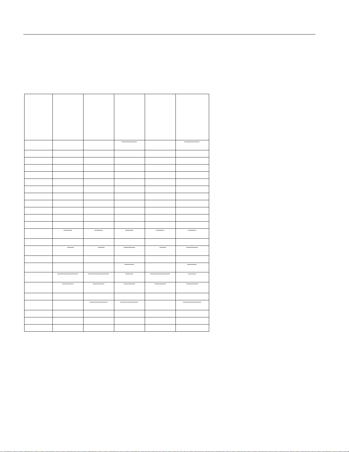
others may require PCB changes. Tables 1 gives the pin functions for the MC146818, DS12885,
DS1685, DS12887, and DS1687 in 24-pin, 600-mil DIP packages.
PIN NAMES - Table 1
Pin #
24-Pin
DIP
MC146818
DS12885
DS1685
DS12887
DS1687
1NCMOT
2OSC1X1 X1 NC NC
3OSC2X2 X2 NC NC
4 AD0 AD0 AD0 AD0 AD0
5 AD1 AD1 AD1 AD1 AD1
6 AD2 AD2 AD2 AD2 AD2
7 AD3 AD3 AD3 AD3 AD3
8 AD4 AD4 AD4 AD4 AD4
9 AD5 AD5 AD5 AD5 AD5
10 AD6 AD6 AD6 AD6 AD6
11 AD7 AD7 AD7 AD7 AD7
12 V
13
14 AS AS ALE AS ALE
15
16 NC Batt GND Batt GND NC NC
17 DS DS
18
19
20 CKFS V
21 CKOUT
22 PS NC V
23 SQW SQW SQW SQW SQW
24 V
SS
CE CS CS CS CS
R/
W R/W WR R/W WR
RESET RESET
IRQ IRQ IRQ IRQ IRQ
DD
GND GND GND GND
BAT
RCLR RCLR
V
CC
PWR
RD
KS RESET KS
V
BAT
BAUX
V
CC
MOT
DS
NC NC
NC
NC V
V
CC
PWR
RCLR
RD
BAUX
V
CC
FUNCTIONAL DIFFERENCES
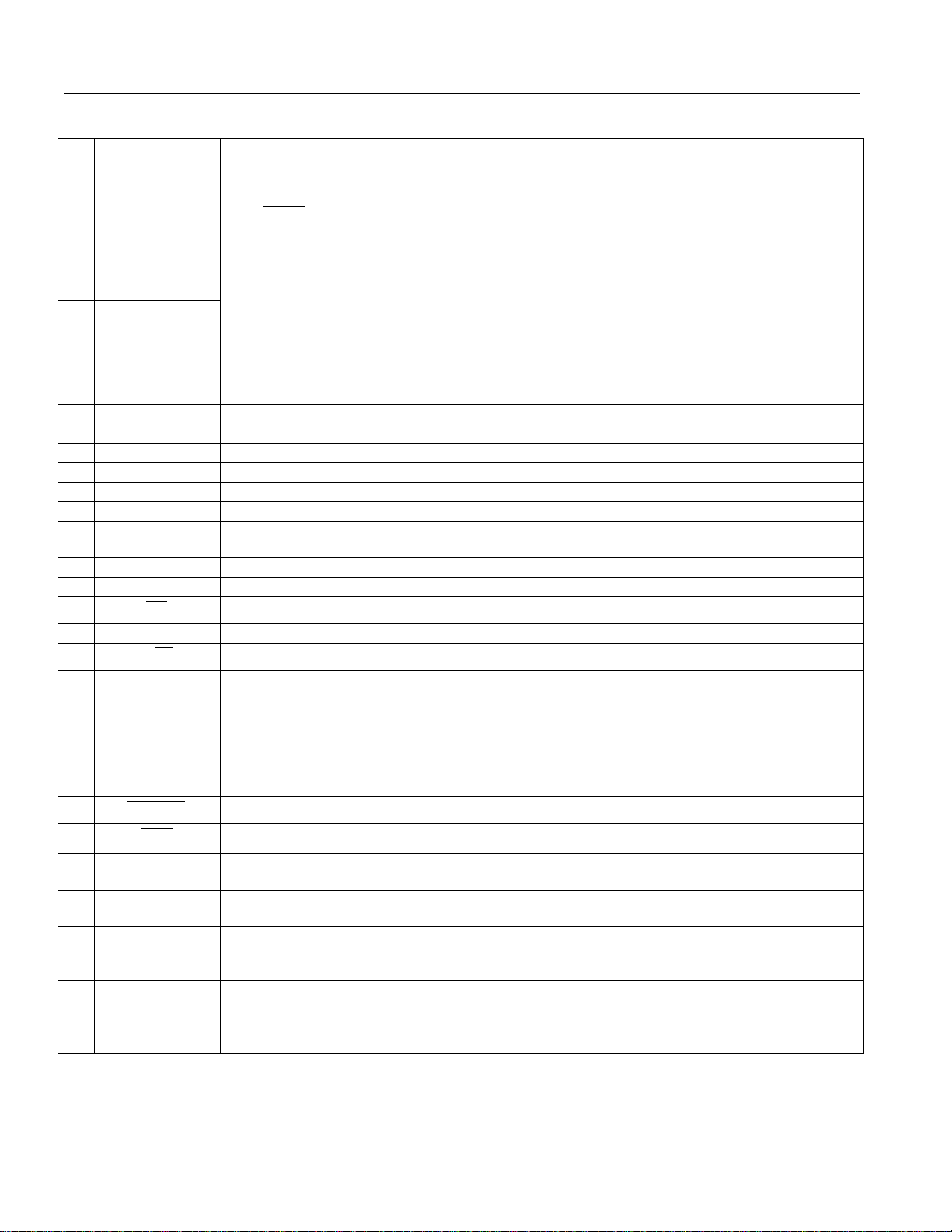
Table 2 summarizes the functional changes by pin for the DS12885 and DS12887. Table 3 has the
changes for the DS1685 and DS1687. These changes will need to be comprehended and the appropriate
modifications made to the board in replacing the MC146818 with any of the Dallas Semiconductor parts.
2 of 5
Page 3

FUNCTIONAL DIFFERENCES - DS12885/87 - Table 2
MC146818 DS12885 DS12887
Pin #
APPLICATION NOTE 521
Replacing the MC146818
If the Motorola bus timing is used, pin 1 needs to be tied to V
1NC
2OSC1
3OSC2
4 AD0 N/A N/A
5 AD1 N/A N/A
6 AD2 N/A N/A
7 AD3 N/A N/A
8 AD4 N/A N/A
9 AD5 N/A N/A
10 AD6
11 AD7 N/A N/A
12 V
13
14 AS N/A N/A
15
16 NC
17 DS N/A N/A
18
19
20 CKFS
21 CKOUT
SS
CE
R/
W
RESET
IRQ
used, then pin 1 can be either tied to ground or left floating. The MC146818 had internal
circuitry to differentiate between the two timing sets.
The MC146818 required external
components along with crystals of 32.768
kHz, 1.048576 MHz, or 4.194304 MHz. The
DS12885 is designed to work with a 32.768
kHz crystal connected directly to pins 2 and
3.
When accessing the clock memory, AD6 on the DS12885/87 needs to be low during the
address strobe. It was a "don't care" on the MC146818.
N/A N/A
N/A N/A
N/A N/A
The negative side of the backup battery
needs to be connected to pin 16 of the
DS12885. The DS12885 handles the
switching to battery power internally and will
disable reads and writes while in back
backup mode.
N/A N/A
N/A N/A
Pin 20 needs to be connected to the positive
side of the backup battery.
The user RAM will be cleared if this pin is
taken low. There is an internal pull-up
resistor, so this pin should be left floating
and not tied high.
The DS12887 does not require an external
crystal, so any components on the board
designed to connect a crystal to this pin may
be removed. The MC146818 would accept
input frequencies of 32.768 kHz, 1.048576
MHz, or 4.194304 MHz. The DS12887
includes a 32.768 kHz crystal in the module.
This pin is a no connect on the DS12887.
On the DS12887A, the
brought out and should be treated the same
as on the DS12885.
. If the Intel bus timing is
CC
N/A
No Connect
RCLR pin is
22 PS
23 SQW N/A N/A
24 V
DD
The MC146818 used this pin to sense the battery voltage and set the VRT bit. This
function is handled internally in the DS12885/87, and the pin is a no connect.
Any on board backup battery that was connected to pin 24 should be removed. The
DS12885 is designed to have the backup battery connected to pins 16 and 20. The
DS12887 has the backup battery included in the module.
3 of 5
Page 4
FUNCTIONAL DIFFERENCES - DS1685/87 - Table 3
MC146818 DS1685 DS1687
Pin #
PWR pin on the DS1685/87 is an output designed to support system power switching
1NC
The
as a result of a date/time alarm (wake up) or a key closure (kickstart).
APPLICATION NOTE 521
Replacing the MC146818
2OSC1
3OSC2
4 AD0 N/A N/A
5 AD1 N/A N/A
6 AD2 N/A N/A
7 AD3 N/A N/A
8 AD4 N/A N/A
9 AD5 N/A N/A
10 AD6
11 AD7 N/A N/A
12 V
13
14 AS N/A N/A
15
16 NC
17 DS N/A N/A
18
19
20 CKFS
21 CKOUT
22 PS
23 SQW N/A N/A
24 V
SS
CS
R/
W
RESET
IRQ
DD
The MC146818 required external
components along with crystals of 32.768
kHz, 1.048576 MHz, or 4.194304 MHz. The
DS1685 is designed to work with a 32.768
kHz crystal connected directly to pins 2 and
3.
When accessing the clock memory, AD6 on the DS1685/87 needs to be low during the
address strobe. It was a "don't care" on the MC146818.
N/A N/A
N/A N/A
N/A N/A
The negative side of the backup battery
needs to be connected to pin 16 of the
DS1685. The DS1685 handles the
switching to battery power internally and will
disable reads and writes while in back
backup mode.
N/A N/A
N/A N/A
This pin needs to be connected to the
positive side of the backup battery.
The user RAM will be cleared if this pin is taken low. There is an internal pull-up resistor,
so this pin should be left floating and not tied high.
The MC146818 used this pin to sense the battery voltage and set the VRT bit. This
function is handled internally in the DS1685/87. This pin is the positive side for an auxiliary
battery required for the kickstart and wake-up features.
Any on board backup battery that was connected to VDD should be removed. The DS1685
is designed to have the backup battery connected to pins 16 and 20 in the DIP and pins 20
and 24 in the PLCC. The DS1687 has the backup battery included in the module.
The DS1687 does not require an external
crystal, so any components on the board
designed to connect a crystal to this pin may
be removed. The MC146818 would accept
input frequencies of 32.768 kHz, 1.048576
MHz, or 4.194304 MHz. The DS1687
includes a 32.768 kHz crystal in the module.
N/A
No Connect
4 of 5
Page 5
APPLICATION NOTE 521
Replacing the MC146818
REGISTER DIFFERENCES
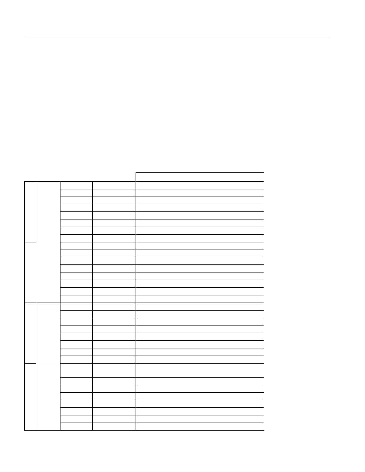
The internal registers contained in memory locations 0A - 0D are used to control the timekeeping,
calendar, and interrupt functions of these parts. In the MC146818 DV2 - DV0 were used to select the
input frequency to provide a proper time base. Since the DS12885/87 and DS1685/87 use only the 32.768
kHz crystal these 3 bits are used to turn the oscillator on or off and to reset the countdown chain. A
pattern of 010 is the only combination of bits that will turn the oscillator on and allow the RTC to keep
time. A pattern of 11X will enable the oscillator but holds the countdown chain in reset. The next update
will occur at 500 ms after a pattern of 010 is written to DV2 - DV0. The VRT bit is maintained internally
in the DS12885/87 and DS1685/87 and will continuously indicate the state of the backup battery voltage.
This bit is read only.
Table 4 contains a list of the registers and the differences that will need to be comprehended in converting
to the DS12885, DS12887, DS1685, or DS1687.
INTERNAL REGISTERS - Table 4
DS12885/87 and DS1685/87
MSB 7 UIP N/A
6DV2 N/A
5 DV1 1-Osc On; 0-Osc off
4 DV0 Must be 0 for timekeeping
3RS3 N/A
Register A
LSB 0 RS0 N/A
MSB 7 SET N/A
Register B
LSB 0 DSE N/A
MSB 7 IRQF N/A
Register C
LSB 0 0 N/A
MSB 7 VRT This bit is read only and should always be 1 to
Register D
LSB 0 0 N/A
2RS2 N/A
1RS1 N/A
6PIE N/A
5AIE N/A
4UIE N/A
3SQWE N/A
2DM N/A
1 24/12 N/A
6PF N/A
5AF N/A
4UF N/A
30 N/A
20 N/A
10 N/A
indicate a good internal battery voltage.
60 N/A
50 N/A
40 N/A
30 N/A
20 N/A
10 N/A
5 of 5
 Loading...