

Page 1
1 of 5 111999
FEATURES
Facilitates uninterruptible power
Uses battery only when primary VCC is not
available
Low forward voltage drop
Power fail signal interrupts processor or write
protects memory
Consumes less than 100 nA of battery current
Low battery warning signal
Battery can be electrically disconnected upon
command
Battery will automatically reconnect when
VCC is applied
Mates directly with DS1212 Nonvolatile
Controller x 16 Chip to back up 16 RAMs
Optional 16-pin SOIC surface-mount package
PIN DESCRIPTION
NC - No Connect
V
BAT
- Battery Input Connection
BF - Battery Fail
Output Signal
BAT - Battery Output
RST - Reset Input
GND - Ground
PF - Power Fail
Output Signal
V
CCO
- RAM Supply
V
CCI
- +5V Supply
PIN ASSIGNMENT
DESCRIPTION
The DS1259 Battery Manager Chip is a low-cost battery management system for portable and nonvolatile
electronic equipment. A battery connected to the battery input pin supplies power to CMOS electronic
circuits when primary power is lost through an efficient switch via the V
CCO
pins. When power is supplied
from the battery, the power-fail signal is active to warn electronic reset circuits of the power status.
Energy loss during shipping and handling is avoided by pulsing reset, thereby causing the battery to be
isolated from other elements in the circuits.
DS1259
Battery Manager Chip
www.dalsemi.com
NC
VBAT
BF
NC
BAT
RST
GND
GND
VCCI
VCCI
VCCO
PF
NC
NC
NC
VCCO
1
2
3
4
5
6
7
8
16
15
14
13
12
11
10
9
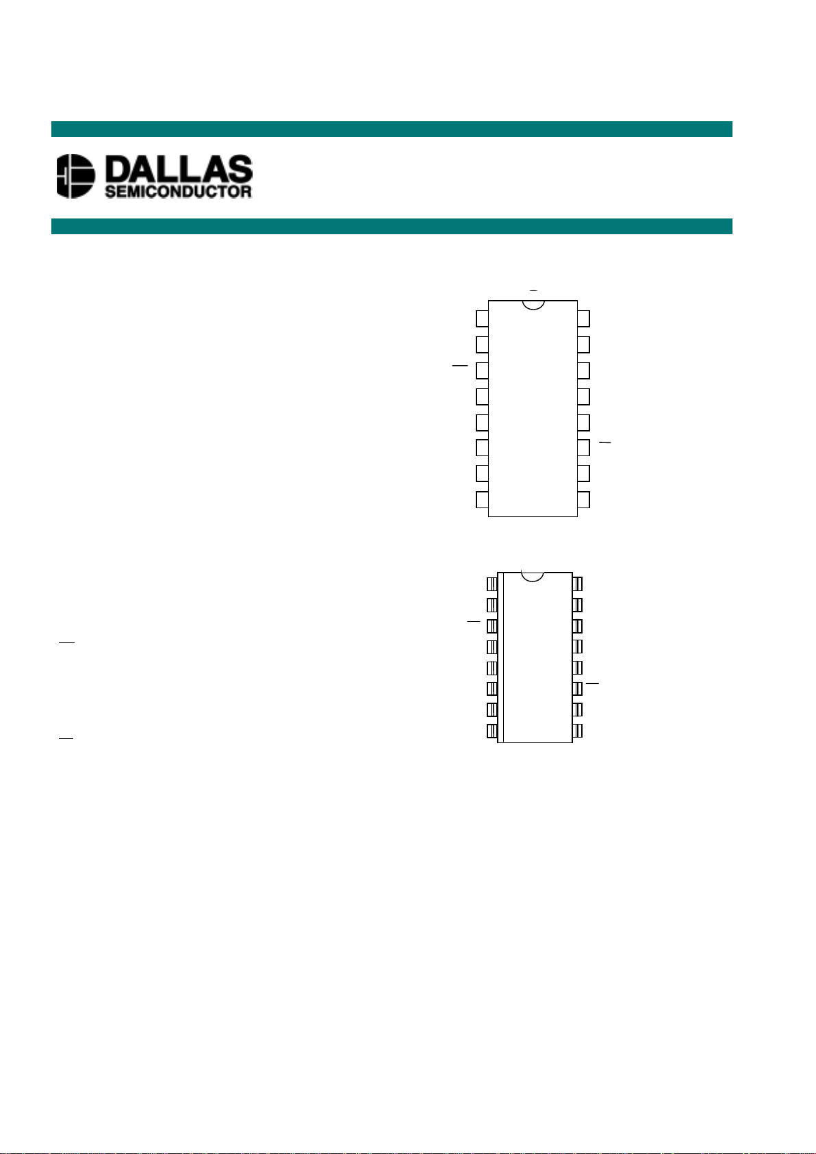
16-Pin DIP Package (300-mil)
See Mech. Drawings Section
NC
VBAT
BF
NC
BAT
RST
GND
GND
VCCI
VCCI
VCCO
PF
NC
NC
NC
VCCO
1
2
3
4
5
6
7
8
16
15
14
13
12
11
10
9
16-Pin SOIC Package (300-mil)
See Mech. Drawings Section
Page 2
DS1259
2 of 5
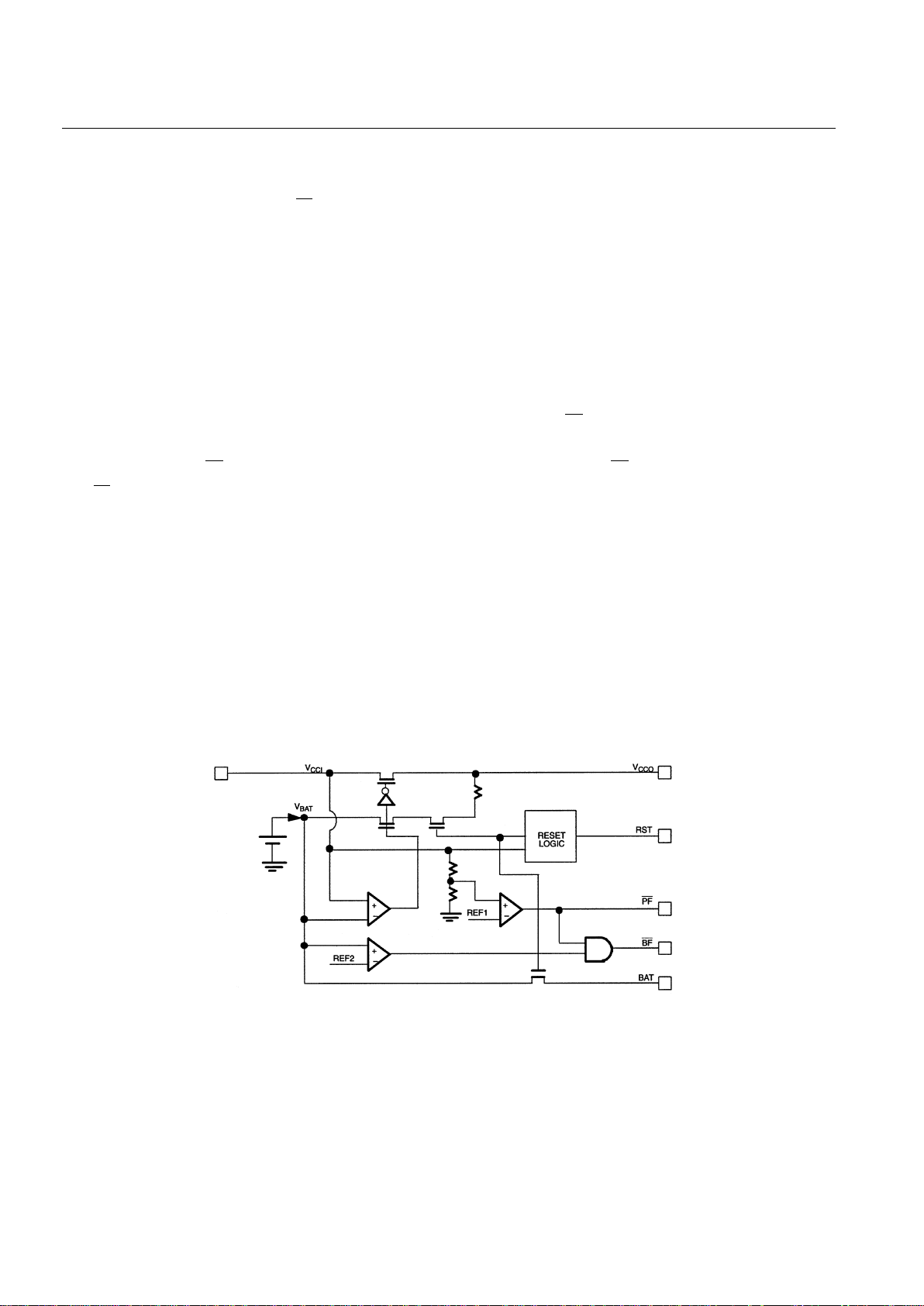
OPERATION
During normal operation, V
CCI
(Pins 15 and 16) is the primary energy source and power is supplied to
V
CCO
(Pins 12 and 13) through an internal switch at a voltage level of V
CCI
-0.2 volts at 250 mA. During
this time the power-fail signal (PF ) is held high, indicating valid V
CCI
voltage (see Figure 1). However, if
the V
CCI
falls below the trip point (V
TP
), a level of 1.26 times the battery level (V
BAT
), the power-fail
signal is driven low. As V
CCI
falls below the battery level, power is switched from V
CCI
to V
BAT
and the
battery supplies power to the uninterruptible output (V
CCO
) at V
BAT
-0.2 volts at 15 mA.
On power-up, as the V
CCI
supply rises above the battery, the primary energy source, V
CCI
, becomes the
supply. As V
CCI
rises above the trip point (VTP), the power fail signal is driven back to the high level.
During normal operation, BAT (Pin 5) stays at the battery level regardless of the level of V
CCI
.
BATTERY FAIL
When power is being supplied from the primary energy source, BF (Pin 3) is held at a high level,
provided that the attached battery (V
BAT
) is greater than 2 volts. If the battery level should decrease to
below 2 volts, the BF signal is driven low, indicating a low battery. The BF signal is always low when
the PF signal is low.
RESET
The reset input can be used to prevent the battery from supplying power to V
CCO
and BAT even if V
CCI
falls below the level of the battery. This feature is activated by applying a pulsed input on RST to high
level for 50ns minimum while primary power is valid (see Figure 2). When primary power is remov ed
after pulsing RST, the V
CCO
output and BAT will go to high impedance. The next time primary power is
applied such that V
CCI
is greater than V
BAT
, normal operation resumes and V
CCO
will be supplied by the
battery or V
CCI
. The BAT output will also return to the level of the battery. Figure 3 shows the DS1259 in
a typical application.
BLOCK DIAGRAM Figure 1
Page 3

DS1259
3 of 5
RESET TIMING Figure 2
TYPICAL APPLICATION Figure 3
Page 4

DS1259
4 of 5
ABSOLUTE MAXIMUM RATINGS*
Voltage on Any Pin Relative to Ground -0.3V to +7.0V
Operating Temperature 0°C to 70°C
Storage Temperature -55°C to +125°C
Soldering Temperature 260°C for 10 seconds
* This is a stress rating only and functional operation of the device at these or any other conditions
above those indicated in the operation sections of this specification is not implied. Exposure to
absolute maximum rating conditions for extended periods of time may affect reliability.
RECOMMENDED DC OPERATING CONDITIONS (0°C to 70°C)
PARAMETER SYMBOL MIN TYP MAX UNITS NOTES
Primary Power Supply V
CCI
5 5.5 V 1
Input High Voltage V
IH
2.0 VCC+0.3 V 1
Input Low Voltage V
IL
-0.3 +0.8 V 1
Battery Voltage Pin 2 V
BAT
2.5 3 3.7 V 6
Battery Output Pin 5 BAT V
BAT
-0.1 V 1
DC ELECTRICAL CHARACTERISTICS (0°C to 70°C; VCC = 4.5 to 5.5V)
PARAMETER SYMBOL MIN TYP MAX UNITS NOTES
Leakage Current I
LO
-1.0 +250 µA
Output Current @ 2.4V I
OH
-1.0 mA 1, 2
Output Current @ 0.4V I
OL
+4.0 mA 1, 2
Input Supply Current I
CCI
10 mA 3
Pins 12, 13 V
CCO=VCCI
-0.2 I
CCO
250 mA
Pin 11 PF Detect
V
TP
(1.26xV
BAT
)
-250mV
(1.26xV
BAT
)
+250mV
V 4, 6
Pin 3 BF Detect
V
BATF
1.5 2.0 2.6 V 7
PARAMETER SYMBOL MIN TYP MAX UNITS NOTES
Pins 12, 13 V
CCO=VBAT
-0.2V I
CCO2
15 mA 5
Battery Leakage I
BAT
100 nA 8
Pin 5 Battery Output Current I
BATOUT
100 µA
CAPACITANCE (TA = 25°C)
PARAMETER SYMBOL MIN TYP MAX UNITS NOTES
Input Capacitance C
IN
510pF
Output Capacitance C
OUT
510pF
AC ELEC TRICAL CHARACTERI STICS (0°C to 70°C; VCC = 4.0 to 5.5V)
PARAMETER SYMBOL MIN TYP MAX UNITS NOTES
V
CCI
Slew Rate t
F
300 µs
V
CCI
Slew Rate t
R
1µs
Power-Down to PF Lo w
t
PF
0µs
PF High after Power-Up
t
REC
100 µs 9
Page 5

DS1259
5 of 5
POWER-DOWN/POWER-UP CONDITION
NOTES:
1. All voltages are referenced to ground.
2. Load capacity is 50 pF.
3. Measured with Pins 11, 12, 13, and 3 open.
4. VTP is the point that PF is driven low.
5. I
CCO2
may be limited by the capability of the battery.
6. Trip point voltage for power-fail detect:
VTP = 1.26 x V
BAT
± 250 mV
For 5% operation: V
BAT
= 3.7V max.
For 10% operation: V
BAT
= 3.5V max.
7. V
BATF
is the point that BF is driven low. These limits are for 0°C to 70°C operation.
8. Battery leakage is the internal energy consumed by the DS1259.
9. V
CC
= +5 volts, tA = 25°C.
 Loading...