

Page 1
www.dalsemi.com
DS1232
MicroMonitor Chip
FEATURES
Halts and restarts an out-of-control
microprocessor
Holds microprocessor in check during power
transients
Automatically restarts microprocessor after
power failure
Monitors pushbutton for external override
Accurate 5% or 10% microprocessor power
supply monitoring
Eliminates the need for discrete components
Space-saving, 8-pin mini-DIP
Optional 16-pin SOIC surface mount package
Industrial temperature -40°C to +85°C
available, designated N
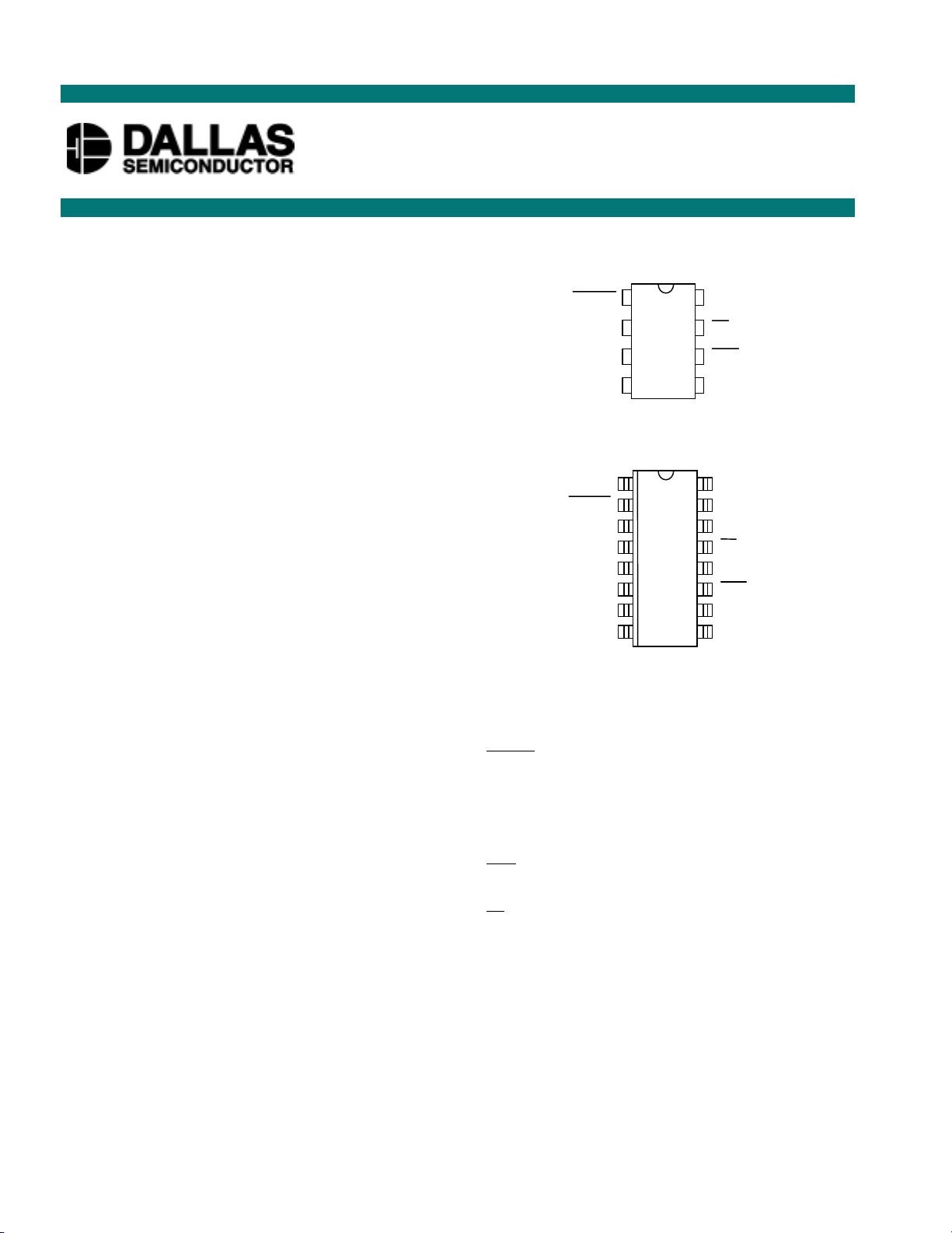
PIN ASSIGNMENT
TD
1
2
3
4
1
2
3
4
5
6
7
8
PBRST
TOL
GND
DS1232 8-Pin DIP (300-mil)
See Mech. Drawings Section
NC
PBRST
NC
TD
NC
TOL
NC
GND
DS1232S 16-Pin SOIC (300-mil)
See Mech. Drawings Section
16
15
14
13
12
11
10
VCC
8
ST
7
RST
6
RST
5
NC
VCC
NC
ST
NC
RST
NC
RST
9
PIN DESCRIPTION
PBRST - Pushbutton Reset Input
TD - Time Delay Set
TOL - Selects 5% or 10% VCC Detect
GND - Ground
RST - Reset Output (Active High)
RST - Reset Output (Active Low, open
drain)
ST - Strobe Input
VCC - +5 Volt Power
NC - No Connections
DESCRIPTION
The DS1232 MicroMonitor Chip monitors three vital conditions for a microprocessor: power supply,
software execution, and external override. First, a precision temperature-compensated reference and
comparator circuit monitors the status of V
power fail signal is generated which forces reset to the active state. When VCC returns to an in-tolerance
condition, the reset signals are kept in the active state for a minimum of 250 ms to allow the power supply
and processor to stabilize.
. When an out-of-tolerance condition occurs, an internal
CC
1 of 7 111899
Page 2

DS1232/DS1232S
The second function the DS1232 performs is pushbutton reset control. The DS1232 debounces the
pushbutton input and guarantees an active reset pulse width of 250 ms minimum. The third function is a
watchdog timer. The DS1232 has an internal timer that forces the reset signals to the active state if the
strobe input is not driven low prior to timeout. The watchdog timer function can be set to operate on
timeout settings of approximately 150 ms, 600 ms, and 1.2 seconds.
OPERATION - POWER MONITOR
The DS1232 detects out-of-tolerance power supply conditions and warns a processor-based system of
impending power failure. When VCC falls below a preset level as defined by TOL (Pin 3), the V
CC
comparator outputs the signals RST (Pin 5) and RST (Pin 6). When TOL is connected to ground, the RST
and RST signals become active as VCC falls below 4.75 volts. When TOL is connected to VCC, the RST
and RST signals become active as VCC falls below 4.5 volts. The RST and RST are excellent control
signals for a microprocessor, as processing is stopped at the last possible moments of valid VCC. On
power-up, RST and
RST are kept active for a minimum of 250 ms to allow the power supply and
processor to stabilize.
OPERATION - PUSHBUTTON RESET
The DS1232 provides an input pin for direct connection to a pushbutton (Figure 2). The pushbutton reset
input requires an active low signal. Internally, this input is debounced and timed such that RST and RST
signals of at least 250 ms minimum are generated. The 250 ms delay starts as the pushbutton reset input is
released from low level.
OPERATION - WATCHDOG TIMER
A watchdog timer function forces RST and RST signals to the active state when the ST input is not
stimulated for a predetermined time period. The time period is set by the TD input to be t ypically 150 ms
with TD connected to ground, 600 ms with TD left unconnected, and 1.2 seconds with TD connected to
VCC. The watchdog timer starts timing out from the set time period as soon as RST and RST are inactive.
If a high-to-low transition occurs on the ST input pin prior to timeout, the watchdog timer is reset and
begins to timeout again. If the watchdog timer is allowed to timeout, then the RST and RST signals are
driven to the active state for 250 ms minimum. The
address signals, data signals, and/or control signals. When the microprocessor is functioning normally,
these signals would, as a matter of routine, cause the watchdog to be reset prior to timeout. To guarantee
that the watchdog timer does not timeout, a high-to-low transition must occur at or less than the minimum
shown in Table 1. A typical circuit example is shown in Figure 3.
ST input can be derived from microprocessor
2 of 7
Page 3
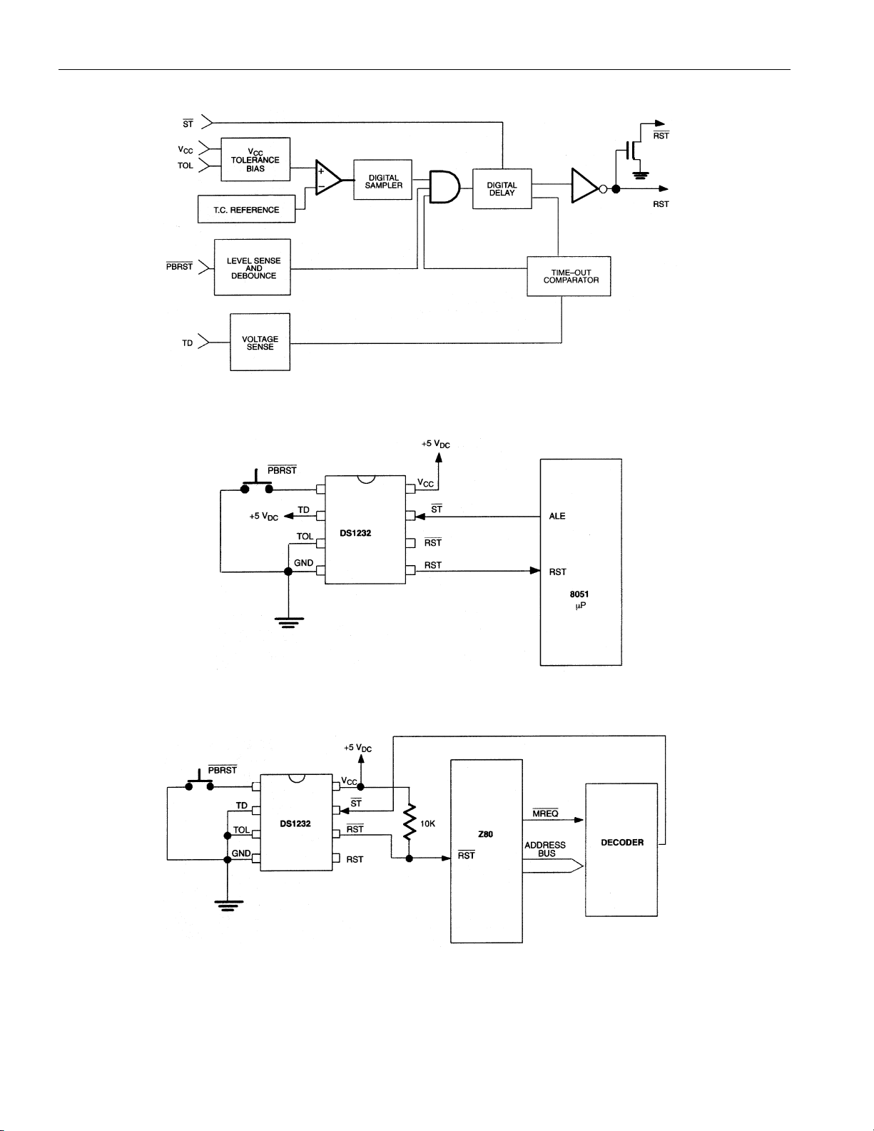
MICROMONITOR BLOCK DIAGRAM Figure 1
PUSHBUTTON RESET Figure 2
DS1232/DS1232S
WATCHDOG TIMER Figure 3
3 of 7
Page 4
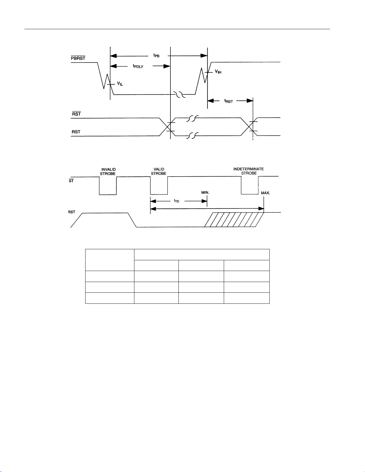
TIMING DIAGRAM: PUSHBUTTON RESET Figure 4
TIMING DIAGRAM: STROBE INPUT Figure 5
DS1232/DS1232S
WATCHDOG TIMEOUTS Table 1
TD PIN
GND 62.5 ms 150 ms 250 ms
Float 250 ms 600 ms 1000 ms
V
CC
500 ms 1200 ms 2000 ms
TIME-OUT
MIN TYP MAX
4 of 7
Page 5
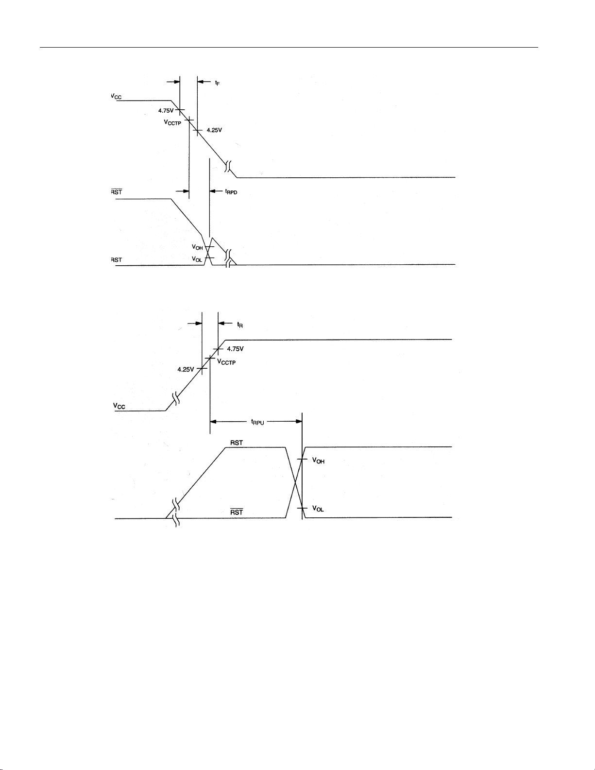
TIMING DIAGRAM: POWER-DOWN Figure 6
TIMING DIAGRAM: POWER-UP Figure 7
DS1232/DS1232S
5 of 7
Page 6
DS1232/DS1232S
ABSOLUTE MAXIMUM RATINGS*
Voltage on V CC Pin Relative to Ground -0.5V to +7.0V
Voltage on I/O Relative to Ground -0.5V to VCC + 0.5V
Operating Temperature 0°C to 70°C
Operating Temperature (Industrial Version) -40°C to +85°C
Storage Temperature -55°C to +125°C
Soldering Temperature 260°C for 10 seconds
* This is a stress rating only and functional operation of the device at these or any other conditions
above those indicated in the operation sections of this specification is not implied. Exposure to
absolute maximum rating conditions for extended periods of time may affect reliability.
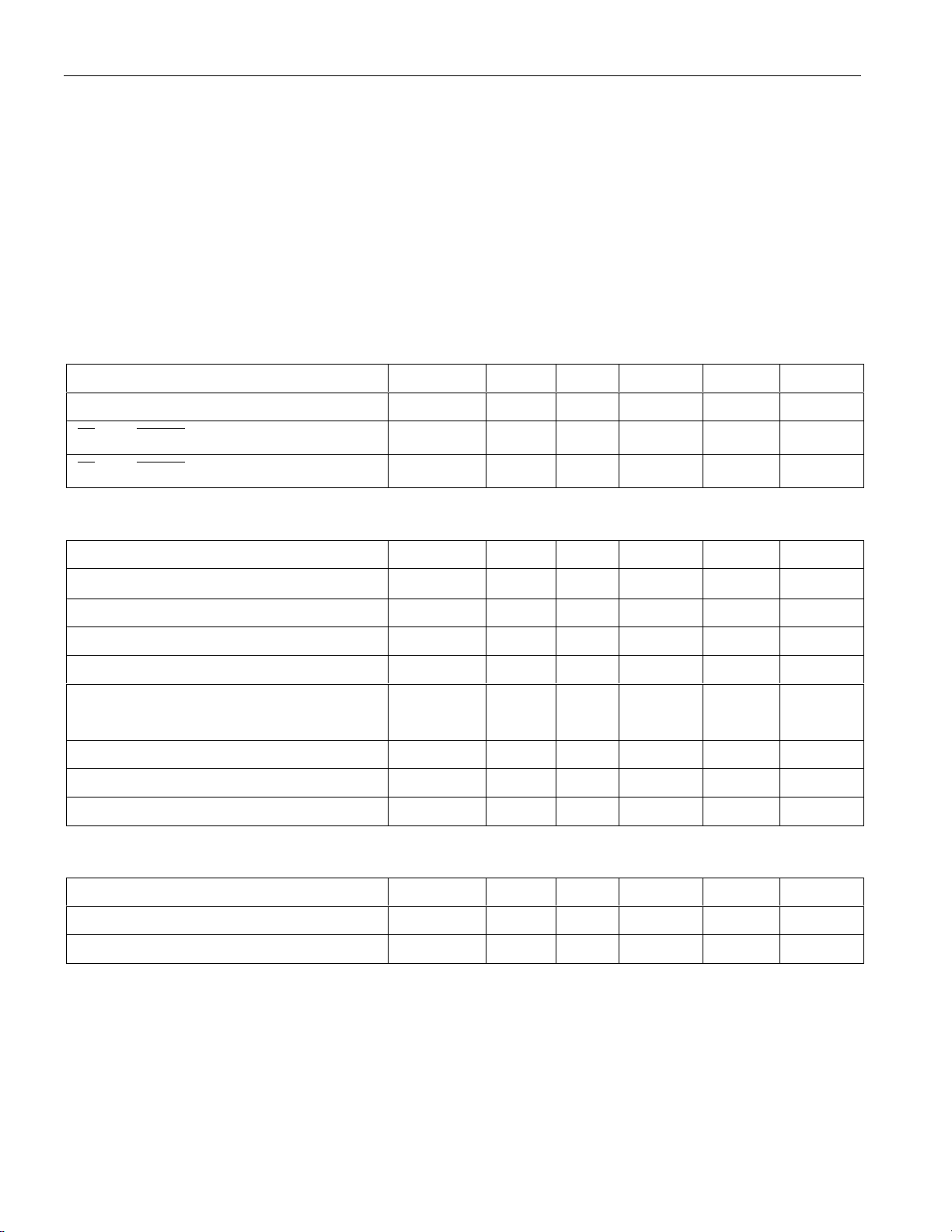
RECOMMENDED DC OPERATING CONDITIONS (0°C to 70°C)
PARAMETER SYMBOL MIN TYP MAX UNITS NOTES
Supply Voltage V
ST and PBRST Input High Level
ST and PBRST Input Low Level
V
V
CC
IH
IL
4.5 5.0 5.5 V 1
2.0 VCC+0.3 V 1
-0.3 +0.8 V 1
DC ELECTRICAL CHARACTERISTICS (0°C to 70°C; VCC=4.5 to 5.5V)
PARAMETER SYMBOL MIN TYP MAX UNITS NOTES
Input Leakage I
Output Current @ 2.4V I
Output Current @ 0.4V I
Low Level @ RST V
Output Voltage @ -500 µA
Operating Current I
VCC Trip Point (TOL=GND) V
VCC Trip Point (TOL=VCC)V
OH
OL
V
CC
CCTP
CCTP
IL
OL
OH
-1.0 +10
µA
-8 -10 mA 5
810 mA
0.4 V 1
V
CC
-0.5V
V
CC
-0.1V
V 1, 7
0.5 2.0 mA 2
4.50 4.62 4.74 V 1
4.25 4.37 4.49 V 1
3
CAPACITANCE (tA=25°C)
PARAMETER SYMBOL MIN TYP MAX UNITS NOTES
Input Capacitance C
Output Capacitance C
IN
OUT
6 of 7
5pF
7pF
Page 7
DS1232/DS1232S
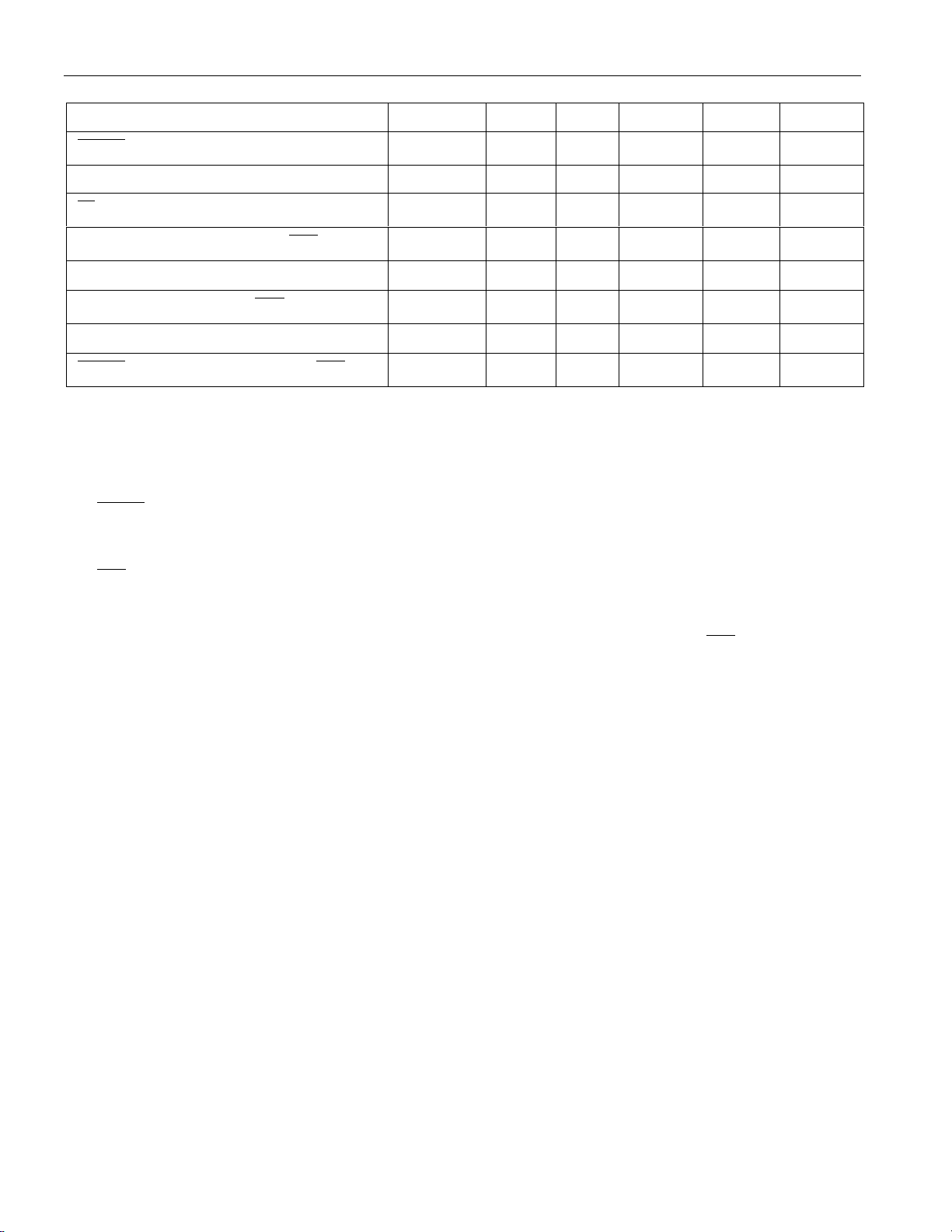
AC ELECTRICAL CHARACTERISTICS (0°C to 70°C; VCC=5V ± 10%)
PARAMETER SYMBOL MIN TYP MAX UNITS NOTES
PBRST = V
IL
RESET Active Time t
ST Pulse Width
VCC Fail Detect to RST and RST
t
VCC Slew Rate 4.75V to 4.25V t
VCC Detect to RST and RST Transition
t
VCC Slew Rate 4.25V to 4.75V t
t
PBRST Stable Low to RST and RST
PDLY
t
PB
RST
t
ST
RPD
F
RPU
R
20 ms
250 610 1000 ms
20 ns 6, 8
100 175
300
250 610 1000 ms 4
05
20 ms
NOTES:
1. All voltages referenced to ground.
2. Measured with outputs open.
3. PBRST is internally pulled up to VCC with an internal impedance of 10k typical.
4. tR = 5 µs.
5. RST is an open-drain output.
µs
µs
µs
6. Must not exceed tTD minimum. See Table 1.
7. RST remains within 0.5V of VCC on power-down until VCC drops below 2.0V. RST remains within
0.5V of GND on power-down until VCC drops below 2.0V.
8. Watchdog can not be disabled. It must be strobed to avoid resets.
7 of 7
 Loading...