

Page 1
DS1231/S
DS1231/S
Power Monitor Chip
FEATURES
• Warns processor of an impending power failure
• Provides time for an orderly shutdown
• Prevents processor from destroying nonvolatile
memory during power transients
• Automatically restarts processor after power is
restored
• Suitable for linear or switching power supplies
• Adjusts to hold time of the power supply
• Supplies necessary signals for processor interface
• Accurate 5% or 10% V
monitoring
CC
• Replaces power-up reset circuitry
• No external capacitors required
• Optional 16-pin SOIC surface mount package
DESCRIPTION
The DS1231 Power Monitor Chip uses a precise temperature-compensated reference circuit which provides
an orderly shutdown and an automatic restart of a processor-based system. A signal warning of an impending
power failure is generated well before regulated DC
voltages go out of specification by monitoring high voltage inputs to the power supply regulators. If line isolation is required a UL-approved opto-isolator can be directly interfaced to the DS1231. The time for processor
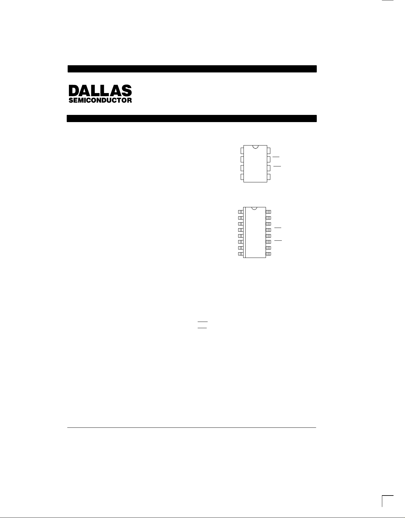
PIN ASSIGNMENT
1
8
IN
2
MODE
3
TOL
4
GND
DS1231 8–Pin DIP
(300 MIL)
See Mech. Drawings
Section
1
NC
2
IN
3
NC
MODE
GND
4
5
NC
6
TOL
7
NC
8
DS1231S 16–Pin SOIC
See Mech. Drawings
(300 MIL)
Section
VCC
NMI
7
RST
6
5
RST
NC
16
15
VCC
NC
14
13
NMI
NC
12
RST
11
10
NC
9
RST
PIN DESCRIPTION
IN – Input
MODE – Selects input pin characteristics
TOL – Selects 5% or 10% V
GND – Ground
RST – Reset (Active High)
RST
NMI
V
CC
– Reset (Active Low, open drain)
– Non–Maskable Interrupt
– +5V Supply
NC – No Connections
shutdown is directly proportional to the available
hold-up time of the power supply. Just before the
hold-up time is exhausted, the Power Monitor unconditionally halts the processor to prevent spurious cycles
by enabling Reset as V
falls below a selectable 5 or
CC
10 percent threshold. When power returns, the processor is held inactive until well after power conditions have
stabilized, safeguarding any nonvolatile memory in the
system from inadvertent data changes.
CC
detect
022698 1/9
Page 2

DS1231/S
OPERATION
The DS1231 Power Monitor detects out-of-tolerance
power supply conditions and warns a processor-based
system of impending power failure. The main elements
of the DS1231 are illustrated in Figure 1. As shown, the
DS1231 actually has two comparators, one for monitoring the input (Pin 1) and one for monitoring V
The VCC comparator outputs the signals RST (Pin 5)
and RST (Pin 6) when VCC falls below a preset trip level
as defined by TOL (Pin 3).
When TOL is connected to ground, the RST and RST
signals will become active as VCC goes below 4.75
volts. When TOL is connected to VCC, the RST and RST
signals become active as VCC goes below 4.5 volts. The
RST and RST signals are excellent control signals for a
microprocessor, as processing is stopped at the last
possible moments of valid V
. On power-up, RST and
CC
RST are kept active for a minimum of 150 ms to allow the
power supply to stabilize (see Figure 2).
The comparator monitoring the input pin produces the
NMI
signal (Pin 7) when the input threshold voltage
(VTP) falls to a level as determined by Mode (Pin 2).
When the Mode pin is connected to V
CC
curs at VTP-. In this mode Pin 1 is an extremely high impedance input allowing for a simple resistor voltage divider network to interface with high voltage signals.
When the Mode pin is connected to ground, detection
occurs at V
+. In this mode Pin 1 sources 30 µA of cur-
TP
rent allowing for connection to switched inputs, such as
a UL-approved opto-isolator. The flexibility of the input
pin allows for detection of power loss at the earliest point
in a power supply system, maximizing the amount of
time allotted between NMI
and RST . On power-up, NMI
is released as soon as the input threshold voltage (VTP)
is achieved and VCC is within nominal limits. In both
(Pin 8).
CC
, detection oc-
modes of operation the input pin has hysteresis for
noise immunity (Figure 3).
APPLICATION – MODE PIN
CONNECTED TO V
When the Mode pin is connected to VCC, pin 1 is a high
impedance input. The voltage sense point and the level
of voltage at the sense point are dependent upon the
application (Figure 4). The sense point may be developed from the AC power line by rectifying and filtering
the AC. Alternatively, a DC voltage level may be selected which is closer to the AC power input than the
regulated +5-volt supply , so that ample time is provided
for warning before regulation is lost.
Proper operation of the DS1231 requires a maximum
voltage of 5 volts at the input (Pin 1), which must be
derived from the maximum voltage at the sense point.
This is accomplished with a simple voltage divider network of R1 and R2. Since the IN trip point V
volts (using the -20 device), and the maximum allowable
voltage on pin 1 is 5 volts, the dynamic range of voltage
at the sense point is set by the ratio of 2.3/5.0=.46 min.
This ratio determines the maximum deviation between
the maximum voltage at the sense point and the actual
voltage which will generate NMI
Having established the desired ratio, and confirming
that the ratio is greater than .46 and less than 1, the
proper values for R1 and R2 can be determined by the
equation as shown in Figure 4. A simple approach to
solving this equation is to select a value for R2 which is
high enough impedance to keep power consumption
low, and solve for R1. Figure 5 illustrates how the
DS1231 can be interfaced to the AC power line when
the mode pin is connected to V
CC
CC
- is 2.3
TP
.
.
022698 2/9
Page 3
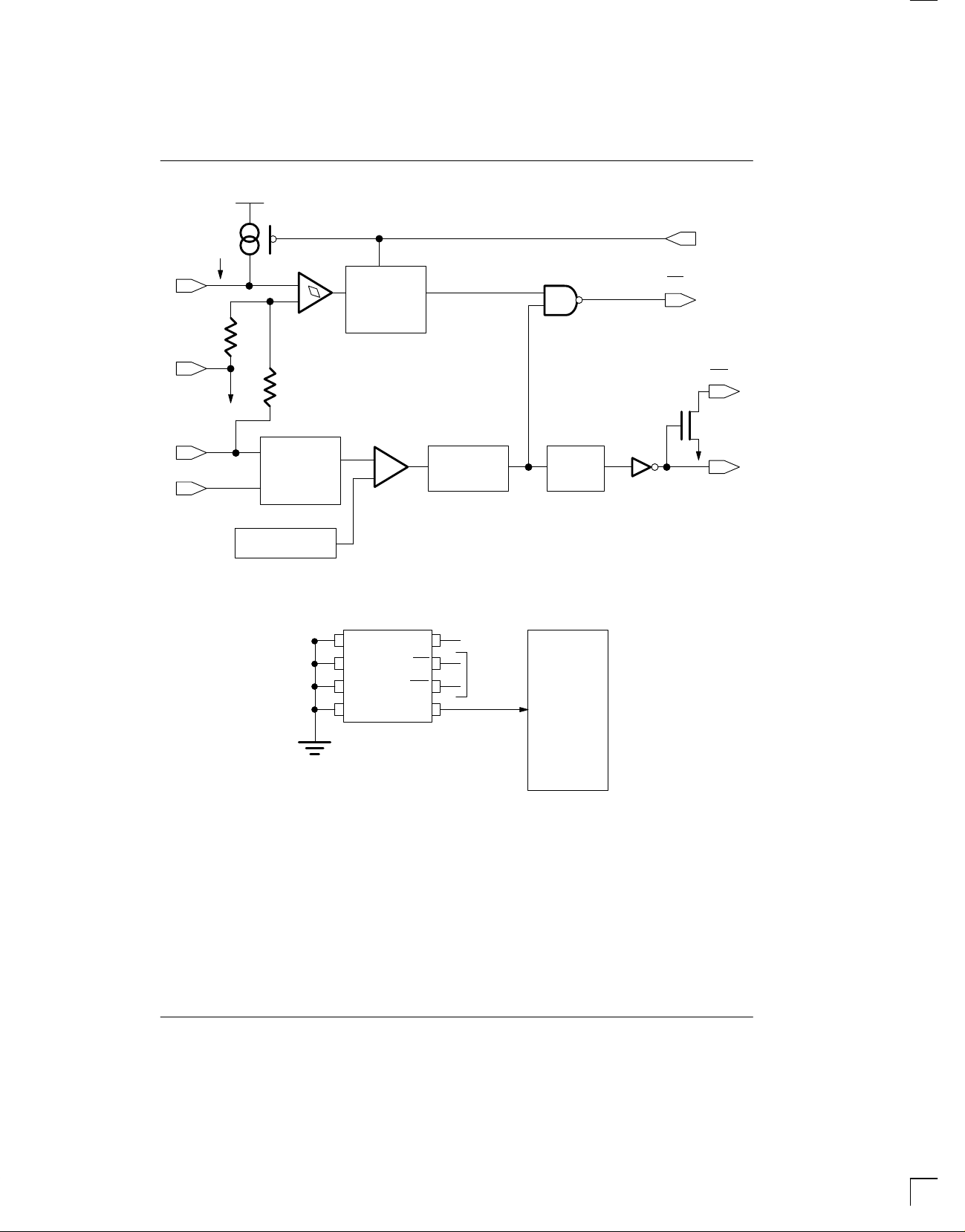
POWER MONITOR BLOCK DIAGRAM Figure 1
30A
IN
1
GND
4
V
CC
8
TOL
3
V
CC
TOLERANCE
BIAS
T.C. REFERENCE
NMI
MODE
SELECTION
DIGITAL
SAMPLER
DIGITAL
DELAY
DS1231/S
MODE
2
NMI
7
RST
6
RST
5
POWER-UP RESET Figure 2
DS1231
IN
MODE
TOL
GND
(-5% VCC THRESHOLD)
V
NMI
RST
RST
CC
+5V
NC
MICROPROCESSOR
RST
8051
µP
022698 3/9
Page 4

DS1231/S
INPUT PIN HYSTERESIS Figure 3
NMI
MODE = GND, VCC = +5V
V
OH
–20
–35
–50
V
TP-
V
OL
NMI
MODE = VCC, VCC = +5V
V
OH
V
OL
V
TP-
TP-
VTP+
VTP+V
V
IN
V
IN
VTP+
NOTE: HYSTERESIS TOLERANCE IS +60 mV
APPLICATION WITH MODE PIN CONNECTED TO VCC Figure 4
VOLTAGE SENSE POINT
IN
MODE
TOL
GND
DS1231
V
NMI
RST
RST
CC
R1
+5V
R2
+5V
2.3
2.5
2.15
2.5
2.0
2.5
TO P
V SENSE
EXAMPLE: V SENSE = 8 VOLTS AT TRIP POINT AND A
MAXIMUM VOLTAGE OF 17.5V WITH R2 = 10K
THEN 8
R1 10K
NOTE: RST requires a pull–up resister.
022698 4/9
R1 R2
R2
10K
(-5% VCC THRESHOLD)
X2.3
X2.3
VMAX
R1 = 25K
V SENSE
VTP
X5.0
Page 5

DS1231/S
APPLICATION – MODE PIN CONNECTED TO
GROUND
When the Mode pin is connected to ground, pin 1 is a
current source of 30 µA with a VTP+ of 2.5 volts. Pin 1 is
held below the trip point by a switching device like an
opto-isolator as shown in Figure 6. Determination of the
sense point has the same criteria as discussed in the
previous application. However, determining component
values is significantly different. In this mode, the maximum dynamic range of the sense point versus desired
trip voltage is primarily determined by the selection of a
zener diode. As an example, if the maximum voltage at
the sense point is 200V and the desired trip point is
the trip point. This is particularly true if power consumption on the high voltage side of the opto-isolator is not an
issue. However, if power consumption is a concern,
then it is desirable to make the value of R1 high. As the
value of R1 increases, the effect of the LED current in
the opto-isolator starts to affect the IN trip point. This can
be seen from the equation shown in Figure 6. R1 must
also be low enough to allow the opto-isolator to sink the
30 µA of collector current required by pin 1 and still have
enough resistance to keep the maximum current
through the opto-isolator’s LED within data sheet limits.
Figure 7 illustrates how the DS1231 can be interfaced to
the AC power line when the mode pin is grounded.
150V , then a zener diode of 150V will approximately set
AC VOLTAGE MONITOR WITH TRANSFORMER ISOLATION Figure 5
VOLTAGE SENSE POINT
DS1231
+5V
IN
MODE
DC
TOL
GND
V
NMI
RST
RST
CC
-10% V
THRESHOLD
CC
+5V
DC
TO µ P
NOTE: RST requires a pull–up resister.
022698 5/9
Page 6

DS1231/S
APPLICATION WITH MODE PIN GROUNDED Figure 6
VOLTAGE SENSE POINT
R1
IF
IC
DS1231
IN
MODE
TOL
-5% VCC THRESHOLD
V
CC
NMI
RST
+5V
DC
TO µ P
GND
VOLTAGE SENSE POINT (TRIP VALUE) VZ
IC
CTR
CTR CURRENT TRANSFER RATIO
IF
VZ ZENNER VOLTAGE
EXAMPLE: CTR = 0.2 IC = 30 µA IF = 150 µA
VOLTAGE SENSE POINT = 105 AND
VZ = 100 VOLTS
30
xR1 R133K
0.2
NOTE: RST
THEN 105 100
requires a pull–up resister.
AC VOLTAGE MONITOR WITH OPTO-ISOLATION Figure 7
DS1231
IN
AC LINE
INPUT
NOTE: RST requires a pull–up resister.
MODE
TOL
GND
RST
V
NMI
RST
RST
IC
XR1
CTR
THRESHOLD
-5% V
CC
+5V
CC
DC
TO µ P
022698 6/9
Page 7

DS1231/S
ABSOLUTE MAXIMUM RATINGS*
Voltage on VCC Pin Relative to Ground -0.5V to +7.0V
Voltage on I/O Relative to Ground -0.5V to V
Operating Temperature 0°C to 70°C
Operating Temperature (Industrial Version) –40°C to +85°C
Storage Temperature -55°C to +125°C
Soldering Temperature 260°C for 10 seconds
* This is a stress rating only and functional operation of the device at these or any other conditions above those
indicated in the operation sections of this specification is not implied. Exposure to absolute maximum rating
conditions for extended periods of time may affect reliability.
CC
+ 0.5V
RECOMMENDED DC OPERATING CONDITIONS (0°C to 70°C)
PARAMETER SYMBOL MIN TYP MAX UNITS NOTES
Supply Voltage V
Input Pin 1 V
CC
IN
4.5 5.0 5.5 V 1
V
CC
V 1
DC ELECTRICAL CHARACTERISTICS (0°C to 70°C; V
= 4.5 to 5.5V)
CC
PARAMETER SYMBOL MIN TYP MAX UNITS NOTES
Low Level @ RST V
Output Voltage @ –500 µA V
Input Leakage I
Output Current @2.4V I
Output Current @0.4V I
Operating Current I
Input Pin 1 (Mode=GND) I
Input Pin 1 (Mode=VCC) I
IN Trip Piont (Mode=GND) V
IN Trip Point (Mode=VCC) V
VCC Trip Point (TOL=GND) V
VCC Trip Point (TOL=VCC) V
OL
OH
IL
OH
OL
CC
C
C
TP
TP
CCTP
CCTP
VCC–0.5V VCC–0.1V V 1, 6
-10 +10 µA 2
1.0 2.0 mA 5
2.0 3.0 mA
0.5 2.0 mA 3
15 25 50 µA
See Figure 3 1
4.50 4.62 4.74 V 1
4.25 4.37 4.49 V 1
CAPACITANCE (T
0.4 V 1
0.1 µA
A
= 25°C)
PARAMETER SYMBOL MIN TYP MAX UNITS NOTES
Input Capacitance C
Output Capacitance C
IN
OUT
5 pF
7 pF
1
022698 7/9
Page 8

DS1231/S
AC ELECTRICAL CHARACTERISTICS (0°C to 70°C; V
= 5V + 10%)
CC
PARAMETER SYMBOL MIN TYP MAX UNITS NOTES
VTP to NMI Delay t
VCC Slew Rate 4.75-4.25V t
VCC Detect to RST and RST t
VCC Detect to NMI t
VCC Detect to RST and RST t
VCC Slew Rate 4.25-4.75V t
IPD
F
RPD
IPU
RPU
R
300 µs
150 500 1000 ms 4
0 ns
1.1 µs
100 ns
200 µs 4
NOTES:
1. All voltages referenced to ground.
= +5.0 volts with outputs open.
2. V
CC
3. Measured with outputs open.
= 5 µs.
4. t
R
is an open drain output and requires a pull–up resister.
5. RST
6. RST remains within 0.5V of V
on power–down until VCC drops below 2.0V . RST remains within 0.5V of
CC
GND on power–down until VCC drops below 2.0V .
TIMING DIAGRAM: POWER-UP
V
TP
MODE=V
CC
INPUT PIN 1
MODE=GND
022698 8/9
V
NMI
t
R
4.5V
CC
4.25V
4.75V
t
IPU
RST
RST
V
OH
t
RPU
V
OH
V
OL
Page 9

TIMING DIAGRAM: POWER-DOWN
V
INPUT PIN 1
MODE=V
CC
INPUT PIN 1
MODE=GND
NMI
TP
V
TP
t
IPD
V
OL
DS1231/S
V
RST
RST
t
F
CC
4.75V
V
CCTP
4.25V
t
RPD
RST SLEWS WITH V
V
OH
V
OL
CC
022698 9/9
 Loading...