

Datasheet DS1217A-64K-25, DS1217A-256K-25, DS1217A-192K-25, DS1217A-16K-25, DS1217A-128K-25 Datasheet (Dallas Semiconductor)
...Page 1
DS1217A
DS1217A
Nonvolatile Read/Write Cartridge
FEATURES
• User-insertable
• Capacity up to 32K x 8
• Standard bytewide pinout facilitates connection to
JEDEC 28-pin DIP socket via ribbon cable
• Data retention greater than 10 years
• Automatic write protection circuitry safeguards
against data loss
• Manual switch unconditionally protects data
• Compact size and shape
• Rugged and durable
• Wide operating temperature range of 0°C to 70°C
PIN ASSIGNMENT
Name Position
Ground
+5 Volts
Write Enable
Address 13
Address 8
Address 9
Address 11
Output Enable
Address 10
Cartridge Enable
Data I/O 7
Data I/O 6
Data I/O 5
Data I/O 4
Data I/O 3
A1
A2
A3
A4
A5
A6
A7
A8
A9
A10
A11
A12
A13
A14
A15
B1
B2
B3
B4
B5
B6
B7
B8
B9
B10
B11
B12
B13
B14
B15
Name
No Connect
Address 14
Address 12
Address 7
Address 6
Address 5
Address 4
Address 3
Address 2
Address 1
Address 0
Data I/O 0
Data I/O 1
Data I/O 2
Ground
OFF – ON
3”
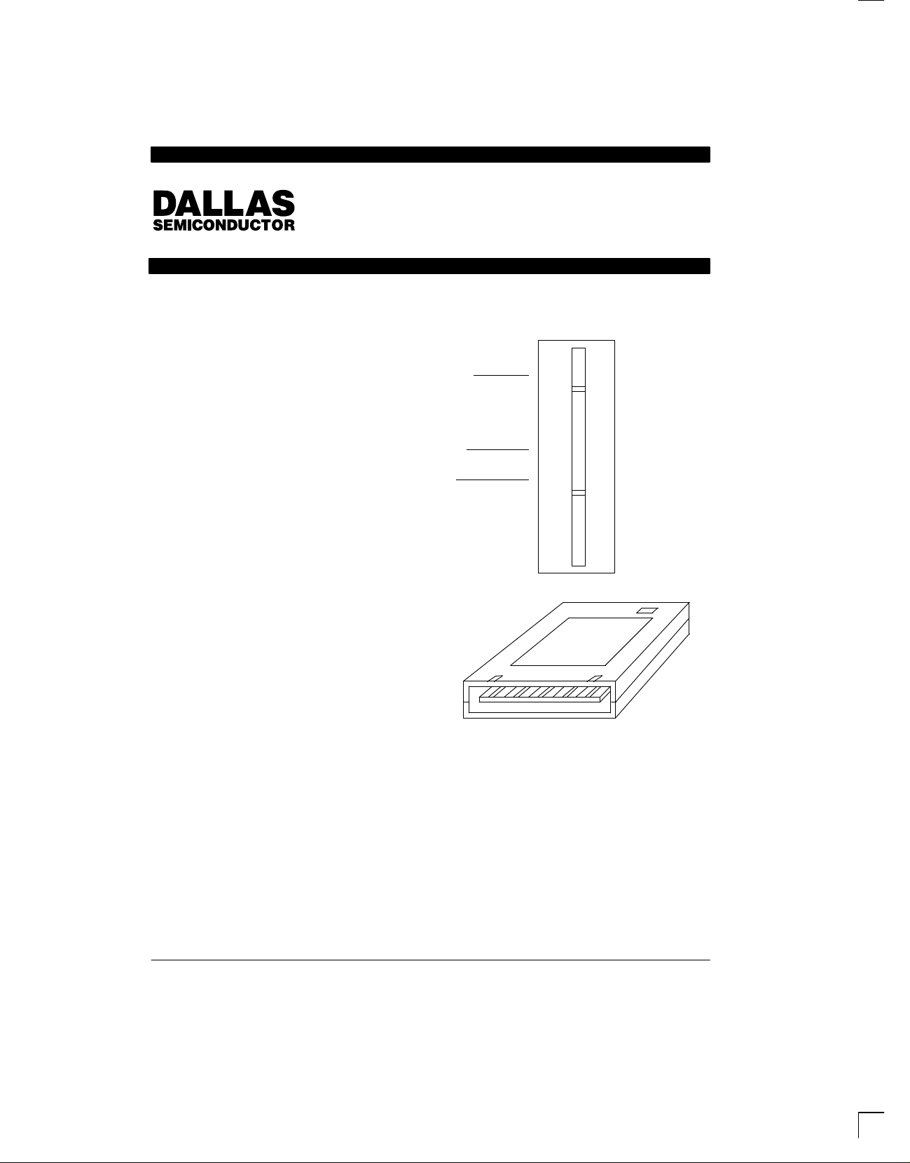
DESCRIPTION
The DS1217A is a nonvolatile RAM designed for portable applications requiring a rugged and durable package. The nonvolatile cartridge is available in densities
ranging from 2K x 8 to 32K x 8 in 8K byte increments. A
card edge connector is required for connection to a host
system. A standard 30-pin connector can be used for direct mount to a printed circuit board. Alternatively, remote mounting can be accomplished with a 28-conductor ribbon cable terminated with a 28-pin DIP plug. The
A1
B1
See Mech. Drawings Section
remote method can be used to retrofit existing systems
that have JEDEC 28-pin bytewide memory sites.
The DS1217A cartridge has a lifetime energy source to
retain data and circuitry needed to automatically protect
memory contents. Reading and writing the memory locations is the same as using conventional static RAM. If
the user wants to convert from read/write memory to
read-only memory, a manual switch is provided to unconditionally protect memory contents.
030598 1/8
Page 2

DS1217A
READ MODE
The DS1217A executes a read cycle whenever WE
(write enable) is inactive (high) and CE (cartridge enable) is active (low). The unique address specified by
the 15 address inputs (A0-A14) defines which of the
32,768 bytes of data is to be accessed. V alid data will be
available to the eight data I/O pins within t
ACC
(access
time) after the last address input signal is stable, providing that CE and OE (output enable) access times are
also satisfied. If OE and CE times are not satisfied , then
data access must be measured from the latter occurring
signal (CE
or OE); the limiting parameter is either tCO for
CE or tOE for OE rather than address access. Read
cycles can only occur when V
volts. When V
is less than 4.5 volts, the memory is
CC
is greater than 4.5
CC
inhibited and all accesses are ignored.
WRITE MODE
The DS1217A is in the write mode whenever both the
and CE signals are in the active (low) state after ad-
WE
dress inputs are stable. The last falling edge to occur of
either CE or WE will determine the start of the write
cycle. The write cycle is terminated by the first rising
edge of either CE or WE. All address inputs must be
kept valid throughout the write cycle. WE
must return to
the high state for a minimum recovery time (tWR) before
another cycle can be initiated. The OE control signal
should be kept inactive (high) during write cycles to
avoid bus contention. However, if the output bus has
been enabled (CE and OE active) then WE will disable
the outputs in t
from its falling edge. Write cycles
ODW
can only occur when VCC is greater than 4.5 volts.
When VCC is less than 4.5 volts, the memory is write
protected.
DATA RETENTION MODE
The Nonvolatile Cartridge provides full functional capability for VCC greater than 4.5 volts and guarantees write
protection for VCC less than 4.5 volts. Data is maintained in the absence of V
port circuitry. The DS1217A constantly monitors VCC.
Should the supply voltage decay , the RAM is automatically write protected below 4.5 volts. As VCC falls below
approximately 3.0 volts, the power switching circuit connects a lithium energy source to RAM. To retain data
without any additional sup-
CC
during power-up, when V
rises above approximately
CC
3.0 volts, the power switching circuit connects the external VCC to the RAM and disconnects the lithium energy
source. Normal RAM operation can resume after V
CC
exceeds 4.5 volts.
The DS1217A checks battery status to warn of potential
data loss. Each time that V
power is restored to the
CC
cartridge, the battery voltage is checked with a precision
comparator. If the battery supply is less than 2.0 volts,
the second memory cycle is inhibited. Battery status
can, therefore, be determined by performing a read
cycle after power-up to any location in memory, recording that memory location content. A subsequent write
cycle can then be executed to the same memory location, altering data. If the next read cycle fails to verify the
written data, the contents of the memory are questionable.
In many applications, data integrity is paramount. For
this reason, the cartridge provides battery redundancy.
The DS1217A features an internal isolation switch that
provides for the connection of two batteries. During battery backup time, the battery with the highest voltage is
selected for use. If one battery fails, the other will automatically take over. The switch between batteries is
transparent to the user. A battery status warning will occur if both batteries are less than 2.0 volts.
REMOTE CONNECTION VIA A RIBBON
CABLE
Existing systems that contain 28-pin bytewide sockets
can be retrofitted using a 28-pin DIP plug. The DIP plug,
AMP Part Number 746616-2, can be inserted into the
28-pin site after the memory is removed. Connection to
the cartridge is accomplished via a 28-pin ribbon cable
connected to a 30-contact card edge connector, AMP
Part Number 499188-4. The 28-pin ribbon cable must
be right-justified such that positions A1 and B1 are left
disconnected. For applications where the cartridge is
installed or removed with power applied, both ground
contacts (A1 and B15) on the card edge connector
should be grounded to further enhance data integrity.
Access time push-out may occur as the distance between the cartridge and driving circuitry is increased.
030598 2/8
Page 3
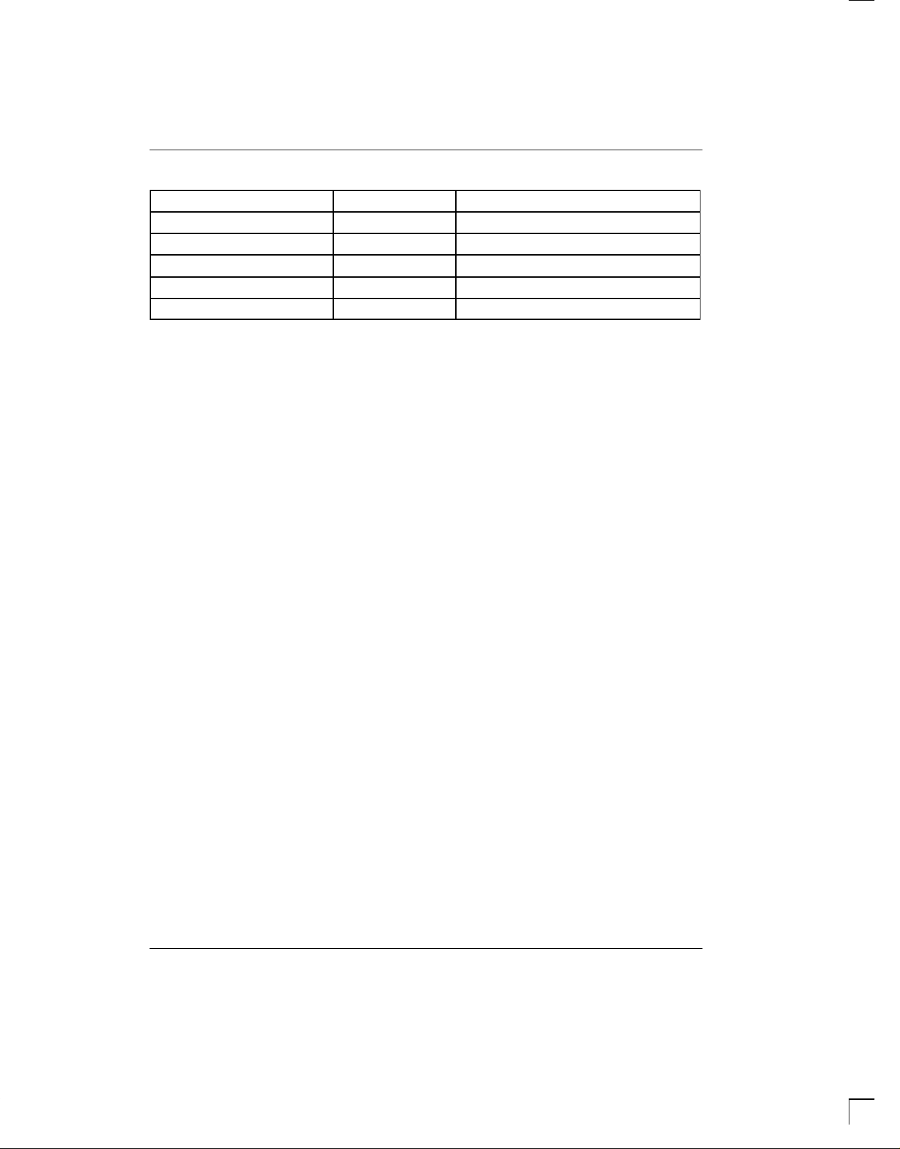
CARTRIDGE NUMBERING Table 1
PART NO. DENSITY UNUSED ADDRESS INPUTS
DS1217A/16K-25 2K x 8 *Address 11, 12, 13, 14
DS1217A/64K-25 8K x 8 *Address 13, 14
DS1217A/128K-25 16K x 8 *Address 14
DS1217A/192K-25 24K x 8
DS1217A/256K-25 32K x 8
*Unused address inputs must be held low (VIL).
DS1217A
030598 3/8
Page 4

DS1217A
ABSOLUTE MAXIMUM RA TINGS*
Voltage on Any Connection Relative to Ground -0.3V to +7.0V
Operating Temperature 0°C to 70°C
Storage Temperature -40°C to +70°C
* This is a stress rating only and functional operation of the device at these or any other conditions above those
indicated in the operation sections of this specification is not implied. Exposure to absolute maximum rating
conditions for extended periods of time may affect reliability.
RECOMMENDED DC OPERATING CONDITIONS (0°C to 70°C)
PARAMETER SYMBOL MIN TYP MAX UNITS NOTES
Power Supply Voltage V
Input High Voltage V
Input Low Voltage V
CC
IH
IL
4.5 5.0 5.5 V
2.2 V
CC
0.0 +0.8 V
V
DC ELECTRICAL CHARACTERISTICS (0°C to 70°C; VCC=5V ± 10%)
PARAMETER SYMBOL MIN TYP MAX. UNITS NOTES
Input Leakage Current I
I/O Leakage Current
VIH V
CE
CC
Output Current @ 2.4V I
Output Current @ 0.4V I
Standby Current CE=2.2V I
Operating Current I
IL
I
IO
OH
OL
CCS1
CCO1
-60 +60 µA
-10 +10 µA
-1.0 -2.0 mA
2.0 3.0 mA
5.0 10 mA
35 75 mA
CAPACITANCE (tA = 25°C)
PARAMETER SYMBOL MIN TYP MAX. UNITS NOTES
Input Capacitance C
Input/Output Capacitance C
030598 4/8
IN
I/O
75 pF
75 pF
Page 5

DS1217A
AC ELECTRICAL CHARACTERISTICS (0°C to 70°C; VCC=5V ± 10%)
PARAMETER SYMBOL MIN TYP MAX UNITS NOTES
Read Cycle Time t
Access Time t
OE to Output Valid t
CE to Output Valid t
OE or CE to Output Active t
Output High Z from
Deselection
Output Hold from
Address Change
Write Cycle Time t
Write Pulse Width t
Address Setup Time t
Write Recovery Time t
Output High Z from WE t
Output Active from WE t
Data Setup Time t
Data Hold Time from WE t
RC
ACC
OE
CO
COE
t
OD
t
OH
WC
WP
AW
WR
ODW
OEW
DS
DH
250 ns
250 ns
125 ns
250 ns
5 ns 5
125 ns 5
5 ns
250 ns
170 ns 3
0 ns
20 ns
100 ns 5
5 ns 5
100 ns 4
20 ns 4
030598 5/8
Page 6

DS1217A
READ CYCLE (1)
ADDRESSES
CE
OE
D
OUT
WRITE CYCLE 1 (2), (6), (7)
ADDRESSES
t
RC
V
IH
V
IL
t
ACC
V
IH
V
IH
V
IH
V
IL
t
AW
t
t
V
COE
COE
t
CO
IL
t
OE
V
IL
V
OH
V
OL
t
WC
V
IH
V
IL
V
IH
V
IH
OUTPUT
DATA VALID
V
IH
V
IL
t
OH
t
OD
t
OD
V
OH
V
OL
V
IH
V
IL
V
IH
V
IL
CE
WE
D
OUT
D
IN
WRITE CYCLE 2 (2), (8)
ADDRESSES
CE
WE
D
OUT
D
IN
t
COE
V
V
IH
t
ODW
V
IH
V
IL
t
AW
V
IH
V
IL
V
t
WC
V
IL
V
IL
t
WP
IL
HIGH
IMPEDANCE
V
V
t
WP
IL
t
ODW
V
IH
V
IL
IH
IL
V
V
V
IL
V
IL
t
DS
IL
IL
t
DS
DATA IN
STABLE
DATA IN
STABLE
t
WR
V
IH
t
OEW
t
DH
V
IH
V
IL
V
IH
V
IL
t
WR
V
IH
V
IH
t
DH
V
IH
V
IL
V
IH
V
IL
030598 6/8
Page 7

POWER-DOWN/POWER-UP CONDITION
V
CC
4.50V
3.2V
DS1217A
t
F
t
PD
t
REC
t
R
CE
LEAKAGE CURRENT
I
SUPPLIED FROM
L
LITHIUM CELL
DATA RETENTION TIME
t
DR
POWER-DOWN/POWER-UP TIMING (0°C to 70°C)
SYM PARAMETER MIN MAX UNITS NOTES
t
t
REC
PD
t
t
CE at V
F
R
V
VCC Slew from 0V to 4.5V (CE at VIH) 0 µs
CE at VIH after Power-Up 2 125 ms 10
before Power-Down 0 µs 10
IH
Slew from 4.5V to 0V (CE at VIH) 100 µs
CC
(tA = 25°C)
SYM PARAMETER MIN MAX UNITS NOTES
t
DR
Expected Data Retention Time 10 years 9
WARNING:
Under no circumstances are negative undershoots, of any amplitude, allowed when the device is in battery backup
mode.
030598 7/8
Page 8

DS1217A
NOTES:
1. WE is high for a read cycle.
= VIH or VIL. If OE = VIH during the write cycle, the output buffers remain in a high impedance state.
2. OE
is specified as the logical AND of CE and WE. tWP is measured from the latter of CE or WE going low to
3. t
WP
the earlier of CE
, tDS are measured from the earlier of CE or WE going high.
4. t
DH
5. These parameters are sampled with a 5pF load and are not 100% tested.
6. If the CE
output buffers remain in a high impedance state during this period.
7. If the CE
output buffers remain in a high impedance state during this period.
8. If WE
is low or the WE low transition occurs prior to or simultaneously with the CE low transition, the output
buffers remains in a high impedance state during this period.
9. Each DS1217A is marked with a 4-digit date code AABB. AA designates the year of manufacture; BB desig-
nates the week of manufacture. The expected t
10.Removing and installing the cartridge with power applied may disturb data.
or WE going high.
low transition occurs simultaneously with or later than the WE low transition in Write Cycle 1, the
high transition occurs prior to or simultaneously with the WE high transition in Write Cycle 1, the
is defined as starting at the date of manufacture.
DR
DC TEST CONDITIONS
Outputs Open
t Cycle = 250ns
All Voltages Are Referenced to Ground
AC TEST CONDITIONS
Output Load: 100pF + 1TTL Gate
Input Pulse Levels: 0 - 3.0V
Timing Measurement Reference Levels
Input: 1.5 V
030598 8/8
 Loading...