

Page 1
1 of 7 111899
FEATURES
Converts full CMOS RAM into nonvolatile
memory
Unconditionally write protects when VCC is
out of tolerance
Automatically switches to battery when
power-fail occurs
4 to 16 decoder provides control for up to 16
CMOS RAMs
Consumes less than 100 nA of battery
current
Tests battery condition on power-up
Provides for redundant batteries
Power fail signal can be used to interrupt
processor on power failure
Optional 5% or 10% power-fail detection
Optional 28-pin PLCC surface mount
package
Optional industrial temperature range of
-40°C to +85°C
PIN DESCRIPTION
A, B, C, D - Address Inputs
CE - Chip Enable
CE0 -CE15 - Chip Enable Outputs
GND - Ground
V
BAT1
- + Battery 1
V
BAT2
- + Battery 2
TOL - Power Supply Tolerance
V
CCI
- +5V Supply
V
CCO
- RAM Supply
PF - Power Fail
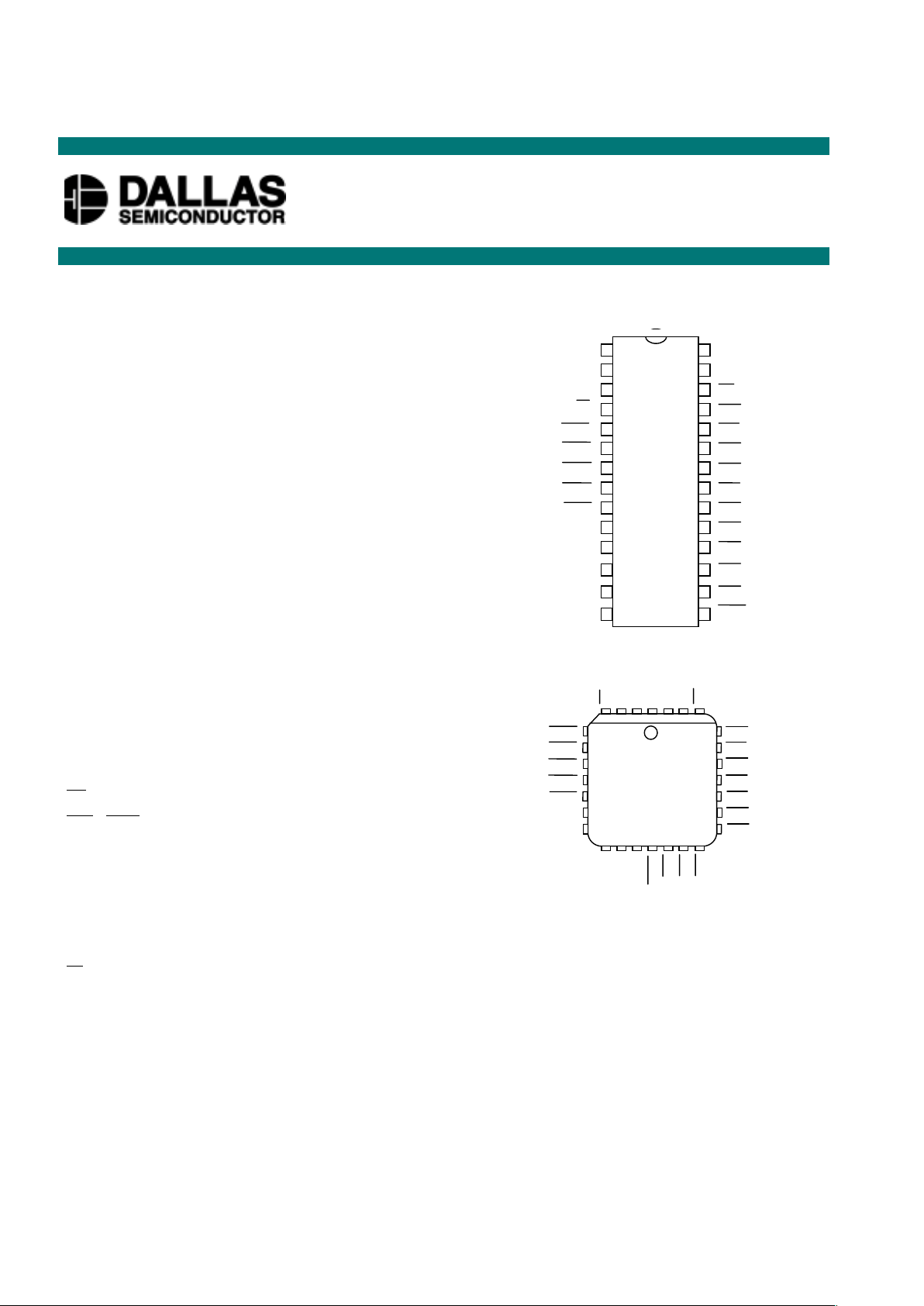
PIN ASSIGNMENT
DESCRIPTION
The DS1212 Nonvolatile Controller x16 Chip is a CMOS circuit that solves the application problem of
converting CMOS RAMs into nonvolatile memories. Incoming power is monitored for an out-oftolerance condition. When such a condition is detected, the chip enables are inhibited to accomplish write
protection and the battery is switched on to supply the RAMs with uninterrupted power. Special circuitry
uses a low-leakage CMOS process that affords precise voltage detection at extremely low battery
consumption.
DS1212
Nonvolatile Controller x 16 Chip
www.dalsemi.com
VBAT1
VCCO
TOL
PF
CE15
CE14
CE13
CE12
CE11
D
C
B
A
GND
VCCI
VBAT2
CE
CE0
CE1
CE2
CE3
CE4
CE5
CE6
CE7
CE8
CE9
CE10
1
2
3
4
5
6
7
8
9
10
11
12
13
14
28
27
26
25
24
23
22
21
20
19
18
17
16
15
28-Pin DIP (600-mil)
See Mech. Drawings Section
28-Pin PLCC
See Mech. Drawings Section
CE15
CE14
CE13
CE12
CE11
D
C
PF
TOL
VCCO
VBAT1
VCCI
VBAT2
CE
25
24
23
22
21
20
19
5
6
7
8
9
10
11
4 3 2 1 28 27 26
12 13 14 15 16 17 18
CE0
CE1
CE2
CE3
CE4
CE5
CE6
B
A
GND
CE10
CE9
CE8
CE7
Page 2

DS1212
2 of 7
By combining the DS1212 Nonvolatile Controller chip and lithium batteries, nonvolatile RAM operation
can be achieved for up to 16 CMOS memories.
OPERATION
The DS1212 performs six circuit functions required to decode and battery back up a bank of up to 16
RAMs. First, the 4-to-16 decoder provides selection of one of 16 RAMs. Second, a switch is provided to
direct power from the battery or V
CCI
supply, depending on which is greater. This switch has a voltage
drop of less than 0.2V. The third function the DS1212 provides is power-fail detection. It constantly
monitors the V
CCI
supply. When V
CCI
falls below 4.75 volts or 4.5 volts, depending on the level of
tolerance Pin 3, a precision comparator outputs a power-fail detect signal to the d ecoder/chip enabl e logi c
and the
PF signal is driven low. The PF signal will remain low until V
CCI
is back in normal limits.
The fourth function of write protection is accomplis hed by holding all chip enable out puts (CE0 - CE15) to
within 0.2 volts of V
CCI
or battery supply. If CE is low at the time power fail detection occurs, the chip
enable outputs are kept in their present state until
CE is driven high. The delay of write protection until
the current memory cycle is completed prevents corruption of data. Power-fail detection occurs in the
range of 4.75 volts to 4.5 volts with tolerance Pin 3 grounded. If Pin 3 is connected to V
CCO
, then powerfail occurs in the range of 4.5 volts to 4.25 volts. During nominal supply conditions the chip enable
outputs follow the logic of a 4-to-16 decoder, shown in Figure 1.
The fifth function the DS1212 performs is a battery status warning so that data loss is avoided. Each time
the circuit is powered up, the battery voltage is checked with a precision comparator. If the battery
voltage is less than 2 volts, the second memory cycle is inhibited. Battery status can, therefore, be
determined by performing a read cycle after power-up to any location in memory, verifying that memory
location content. A subsequent write cycle can then be executed to the same memory location, altering the
data. If the next read cycle fails to verify the written data, then the batteri es are less than 2.0 volts and
data is in danger of being corrupted.
The sixth function of the DS1212 provides for battery redundancy. In many applications, data integrity is
paramount. In these applications it is often desirable to use two batteries to ensure reliability. The
DS1212 provides an internal isolation switch which allows the connection of two batteries during b attery
backup operation. The battery with the highest voltage is selected for use. If one battery should fail, the
other will then assume the load. The switch to a redundant battery is transparent to circuit operation and
the user. A battery status warning will only occur if both batteries are less than 2.0 volts. For single
battery applications the unused battery input must be grounded.
Page 3

DS1212
3 of 7
NONVOLATILE CONTROLLER/DECODER Figure 1
INPUTS OUTPUTS
CE
DCBA
CE0 CE1 CE2 CE3 CE4 CE5 CE6 CE7 CE8 CE9 CE10 CE11 CE12 CE13 CE14 CE15 PF
HXXXXHHHHHHHHHHHHHHHHH
XXXXXHHHHHHHHHHHHHHHHL
LLLLLLHHHHHHHHHHHHHHHH
LLLLHHLHHHHHHHHHHHHHHH
LLLHLHHLHHHHHHHHHHHHHH
LLLHHHHHLHHHHHHHHHHHHH
LLHLLHHHHLHHHHHHHHHHHH
LLHLHHHHHHLHHHHHHHHHHH
LLHHLHHHHHHLHHHHHHHHHH
LLHHHHHHHHHHLHHHHHHHHH
LHLLLHHHHHHHHLHHHHHHHH
LHLLHHHHHHHHHHLHHHHHHH
LHLHLHHHHHHHHHHLHHHHHH
LHLHHHHHHHHHHHHHLHHHHH
LHHLLHHHHHHHHHHHHLHHHH
LHHLHHHHHHHHHHHHHHLHHH
LHHHLHHHHHHHHHHHHHHLHH
LHHHHHHHHHHHHHHHHHHHLH
H = High Level
L = Low Level
X = Irrelevant
Note: V
CCI
input is 250 mV lower when TOL PIN3 = V
CCO
.
Page 4

DS1212
4 of 7
ABSOLUTE MAXIMUM RATINGS*
Voltage on Any Pin Relative to Ground -0.3V to +7.0V
Operating Temperature 0°C to 70°C
Storage Temperature -55°C to +125°C
Soldering Temperature 260°C for 10 seconds
* This is a stress rating only and functional operation of the device at these or any other conditions
above those indicated in the operation sections of this specification is not implied. Exposure to
absolute maximum rating conditions for extended periods of time may affect reliability.
RECOMMENDED DC OPERATING CONDITIONS (0°C to 70°C)
PARAMETER SYMBOL MIN TYP MAX UNITS NOTES
Pin 3 = GND Supply Voltage V
CCI
4.75 5.0 5.5 V 1
Pin 3 = V
CCO
Supply Voltage V
CCO
4.5 5.0 5.5 V 1
Logic 1 Input V
IH
2.2 VCC+0.3 V 1
Logic 0 Input V
IL
-0.3 +0.8 V 1
Battery Input V
BAT1
,
V
BAT2
2.0 4.0 V 1, 2
(0°C to 70°C; V
CCI
= 4.75 to 5.5V PIN 3 = GND)
(0°C to 70°C; V
CCI
= 4.5 to 5.5V, PIN 3 = V
CCO
)
DC ELECTRICAL CHARACTERISTICS
PARAMETER SYMBOL MIN TYP MAX UNITS NOTES
Supply Current I
CCI
5mA3
Supply Current @
V
CCO
= V
CCI
-0.2
I
CCO1
80 mA 1, 4 ,10
Input Leakage I
IL
-1.0 +1.0 µA
Output Leakage I
LO
-1.0 +1.0 µA
CE0 - CE15 , PF Output @ 2.4V
I
OH
-1.0 mA 5
CE0 - CE15 , PF Output @ 0.4V
I
OL
4.0 mA 5
VCC Trip Point (TOL=GND) V
CCTP
4.50 4.62 4.74 V 1
VCC Trip Point (TOL=V
CCO
)V
CCTP
4.25 4.37 4.49 V 1
(0°C to 70°C; V
CCI
< V
BAT
)
PARAMETER SYMBOL MIN TYP MAX UNITS NOTES
CE0 -CE15 Output
V
OHL
V
BAT
-0.2 V 3, 7
Battery Current I
BAT
0.1 µA 2, 3
Battery Backup Current
@ V
CCO
= V
BAT1
– 0.5V
I
CC2
100 µA 6, 10, 11
Page 5

DS1212
5 of 7
CAPACITANCE (TA = 25°C)
PARAMETER SYMBOL MIN TYP MAX UNITS NOTES
Input Capacitance C
IN
5pF
Output Capacitance C
OUT
7pF
(0°C to 70°C; V
CCI
= 4.75 to 5.5V, PIN 3 = GND)
(0°C to 70°C; V
CCI
= 4.5 to 5.5V, PIN 3 = V
CCO
)
AC ELECTRICAL CHARACTERISTICS
PARAMETER SYMBOL MIN TYP MAX UNITS NOTES
CE Propagation Delay
t
PD
51020ns5
CE High to Power-Fail
t
PF
0ns
Address Setup t
AS
20 ns 9
(0°C to 70°C; V
CCI
< 4.75V, PIN 3 = GND)
(0°C to 70°C; V
CCI
< 4.5V, PIN 3 = V
CCO
)
PARAMETER SYMBOL MIN TYP MAX UNITS NOTES
Recovery at Power-Up t
REC
2 80 125 ms
VCC Slew Rate Power-Down t
F
300 µs
VCC Slew Rate Power-Down t
FB
10 µs
VCC Slew Rate Power-Up t
R
0µs
CE Pulse Width
t
CE
1.5 µs 7, 8
Power Fail to PF Low
t
PFL
300 µs
Page 6

DS1212
6 of 7
TIMING DIAGRAM: DECODER
TIMING DIAGRAM: POWER-UP
TIMING DIAGRAM: POWER-DOWN
Page 7

DS1212
7 of 7
TYPICAL APPLICATION Figure 2
OUTPUT LOAD Figure 3
NOTES:
1. All voltages referenced to ground.
2. Only one battery input is required.
3. Measured with V
CCO
and CE0 -CE15 open.
4. I
CC01
is the maximum average load which the DS1212 can supply to the memories.
5. Measured with a load as shown in Figure 3.
6. I
CC02
is the maximum average load current which the DS1212 can supply to the memories in the battery backup
mode.
7. Chip enable outputs
CE0 -CE15 can only sustain leakage current in the battery backup mode.
8. t
CE
max. must be met to ensure data integrity on power loss.
9. t
AS
is only required to keep the decoder outputs glitch-free. While CE is low, the outputs ( CE0 - CE15 ) will be
defined by inputs A through D with a propagation delay of t
PD
from an A through D input change.
10. For applications where higher currents are required, please see the Battery Manager chip data sheet (DS1259).
11. The DS1212 has a 5 kohm resistor in series with the battery input. As current from the battery increases over
100 µA, the voltage drop will increase proportionately. The device cannot be damaged by higher currents in the
battery path.
 Loading...