

Page 1
查询DS1207供应商
DS1207
DS1207
TimeKey
FEATURES
• Cannot be deciphered by reverse engineering
• Time allotment from one day to 512 days for trial
periods, rentals, and leasing
• Partitioned memory thwarts pirating
• User-insertable packaging allows personal
possession
• Exclusive blank keys on request
• Appropriate identification can be made with a 64-bit
reprogrammable memory
• Unreadable 64-bit match code virtually prevents
discovery by exhaustive search with over 10
possibilities
• Random data generation on incorrect match codes
obscures real accesses
• 384 bits of secure read/write memory create
additional barriers by permitting data changes as
often as needed
• Rapid erasure of identification, security match code
and secure read/write memory can occur if tampering
is detected
• Durable and rugged
• Applications include software authorization, gray
market software protection, proprietary data, financial
transactions, secure personnel areas, and system
access control
PIN ASSIGNMENT
DALLAS
DS1207
TimeKey
SIDE
19
15
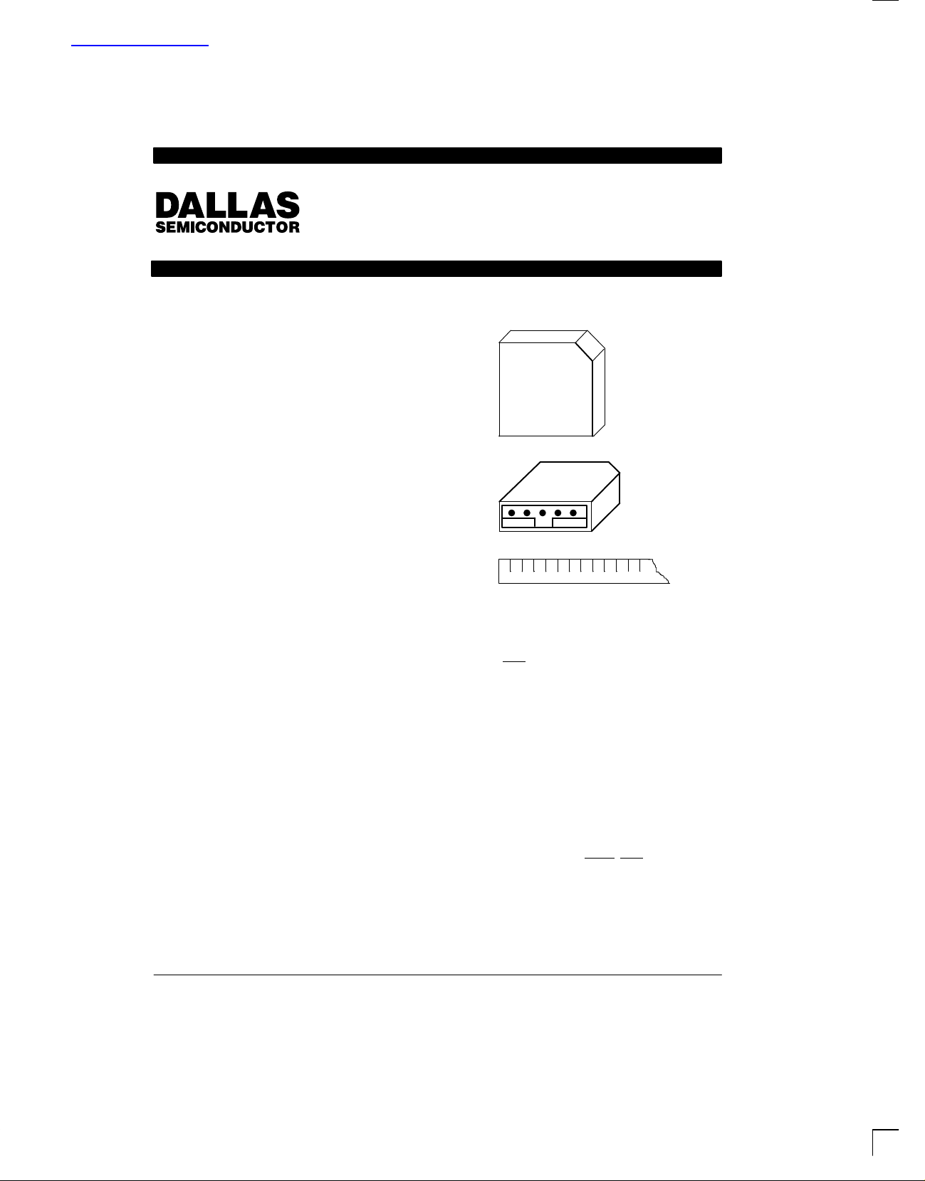
BOTTOM: PIN VIEW
See Mech. Drawings Section
PIN DESCRIPTION
Pin 1 NC No connection
Pin 2 RST Reset
Pin 3 DQ Data input/output
Pin 4 CLK Clock
Pin 5 GND Ground
1.0 IN
DESCRIPTION
The DS1207 TimeKey is a miniature security system
that stores 64 bits of user-definable identification code
and a 64-bit security match code that protects 384 bits of
read/write nonvolatile memory . The 64-bit identification
code and the security match code are programmed into
the TimeKey via a special program mode operation. After programming, the TimeKey follows a procedure with
a serial format to retrieve or update data. The TimeKey
is set to expire from one day to 512 days or infinity, as
specified by the customer. The T imeKey starts its countdown from the first access by the end user.
Interface cost to a microprocessor is minimized by
on-chip circuitry that permits data transfer with only
three signals: Clock (CLK), Reset
Output (DQ). Low pin count and a guided entry for a
mating receptacle overcome mechanical problems normally encountered with conventional integrated circuit
packaging, making the device transportable and
user-insertable.
(RST) and Data Input/
021798 1/17
Page 2

DS1207
OPERATION – NORMAL MODE
The TimeKey has two modes of operation: normal and
program. The normal mode of operation provides the
functions of reading and writing the 384-bit secure
memory. The block diagram (Figure 1) illustrates the
main elements of the TimeKey when used in the normal
mode. T o initiate data transfer with the T imeKey , RST
taken high and 24 bits are loaded into the command register on each low-to-high transition of the CLK input. The
command register must match the exact bit pattern
which defines normal operations with a function code of
read or write. If one of these patterns is not matched,
communications are ignored. If the command register is
loaded properly , communications are allowed to continue. Data is clocked out of the TimeKey on the
high-to-low transition of the clock. If the pattern matched
in the command register calls for a normal read or write,
the next 64 cycles following the command word are read
and data is clocked out of the identification memory. The
next 64 write cycles are written to the compare register
(Figure 2). These 64 bits must match the exact pattern
stored in the security match memory. If a match is not
found, access to additional information is denied. Instead, if a normal read mode is selected, random
garbled data is output for the next 384 cycles. If a normal
write cycle is selected and a match is not achieved, the
TimeKey will ignore any additional information. However, when a security match is achieved, access is permitted to write the 384-bit secure memory .
OPERATION - PROGRAM MODE
The program mode of operation provides the functions
of programming the identification and security match
memory, and setting and reading the amount of time the
TimeKey can be used. The block diagram in Figure 3 illustrates the main elements of the TimeKey when used
in the program mode. T o initiate the program mode, RST
is driven high and 24 bits are loaded into the command
register on each low-to-high transition of the CLK input.
The command register must match the exact bit pattern
that defines the program mode for the identification and
security match bits or the program mode for setting and
reading the amount of time for which the TimeKey can
be used. If an exact match for one of the seven function
codes of the program mode is not found, the remainder
of the program mode is ignored. When the command
register is properly loaded for programming the identification and security match bits, the next 128 bits are written to the identification and security match memory
(Figure 4). When this mode of operation is invoked, all
memory contents are erased.
SETTING AND READING TIME REMAINING
There are six functions of the program mode which are
used to set or read the amount of time for which the
TimeKey will allow full operation. T o initiate any of the six
functions of the program mode used for setting and
reading time remaining, RST
is
are loaded into the command register on each
low-to-high transition of the CLK input. If the command
register is properly loaded with the function code for
reading the 20-bit day clock counter, the next 20 bits will
be output (LSB first) as a binary count of the amount of
time elapsed in the current day (see Figure 5). The time
can be calculated by dividing this count reading by 2
(20 bits is equal to 1,048,576 counts). One minus this result is the fraction of a day remaining. The 20-bit day
clock counter is driven by an internal oscillator that has a
period of 82.4 ms. If the command register is properly
loaded with the function code for reading the 9-bit number of days counter, the next 9 bits will be output (LSB
first) as a binary count of the days remaining (see
Figure 6). This count is decremented each time the day
clock counter rolls over to zero. When the number of
days remaining counter rolls through zero, normal and
program mode write cycles are inhibited. If the program
mode read cycle to the number of days counter is attempted, the nine bits will be returned as all ones.
If the command register is properly loaded with the function code for writing the 9-bit number of days counter,
the next nine bits will be input (LSB first) as a binary
count of the desired number of days in which the TimeKey will be fully functional (see Figure 7). The number of
days counter can be changed by writing over an entered
value as often as required until the lock command is entered. The lock command is given when the command
register is properly loaded with the function code for
locking up the number of days counter. The lock command consists of the 24-bit command word only (see
Figure 8). Once the lock command is given, all future
write cycles to the number of days register are ignored.
After the correct value has been written and locked into
the number of days counter, the DS1207 will start counting the time from the entered value to zero after the first
access to the TimeKey is executed, provided the arm
oscillator bit is set. The arm oscillator bit is set when the
command register has been properly loaded with the
function code for arming the oscillator. The arm oscillator command consists of the 24-bit command word only
(see Figure 9). One other command is also available for
use in setting and reading time remaining. A stop oscillator command is given when the command register is
is driven high and 24 bits
20
021798 2/17
Page 3

DS1207
properly loaded with the function code for stopping the
oscillator. The stop oscillator command consists of the
24-bit command word only (see Figure 10). This command will only execute prior to issuing a lock command.
After the lock command is issued, stop oscillator commands are ignored.
A sequence for properly setting the expiration time of
the DS1207 is as follows (see Figure 1 1). First, program
the identification and security match bits to the desired
value. Use normal mode operation to write the appropriate secure data. Second, write the number days remaining register to the desired value. This number can be immediately verified by reading the number of days
remaining. Next, arm the oscillator by writing the appropriate command. Then do a normal mode read. This action will start the internal oscillator. Now read the 20-bit
day clock counter several times to verify that the oscillator is running. After oscillator activity has been verified,
issue the stop oscillator command. The lock command
should be issued, followed by the arm oscillator command. The TimeKey will start the countdown to expiration on the next access. T o guarantee security , a locked
TimeKey cannot be unlocked. The key cannot be reprogrammed after expiration. The oscillator verification
portion of this sequence is not required and can be deleted when speed in setting time remaining is important.
COMMAND WORD
Each data transfer for normal and program mode begins
with a 3-byte command word as shown in Figure 12. As
defined, the first byte of the command word specifies the
function code. Eight function codes are acceptable
(Figure 13). If any one of the bits of the first byte of the
command word fails to meet one of the exact patterns
for function codes, the data transfer will be aborted.
count, lock number of days count, arm oscillator, and
stop oscillator.
The remaining six bits of byte 2 and the first four bits of
byte 3 must be written to match one of the five patterns
as indicated in Figure 12 or data transfer will abort. Under special contract with Dallas Semiconductor, these
bits can be defined by the user as any bit pattern other
than those specified as unavailable. The bit pattern as
defined by the user must be written exactly or data
transfer will abort. The last four bits of byte 3 of the command word must be written 1011 or data transfer will
abort. Table 1 provides a summary of the command
words in hexadecimal as they apply to all function codes
for both program mode and normal mode.
RESET AND CLOCK CONTROL
All data transfers are initiated by driving the RST input
high. The reset input serves three functions. First, it
turns on control logic which allows access to the command register for the command sequence. Second, the
RST signal provides a power source for the cycle to follow. To meet this requirement, a drive source for RST
2 mA at 3.5 volts is required. Third, the RST
signal pro-
vides a method of terminating data transfer.
A clock cycle is a sequence of a falling edge followed by
a rising edge. For data inputs, the data must be valid
during the rising edge of the clock cycle. Command bits
and data bits are input on the rising edge of the clock.
Data bits are output on the falling edge of the clock. The
rising edge of the clock returns the DQ pin to a high impedance state. All data transfer terminates if the RST
pin is low and the DQ pin goes to a high impedance
state. Data transfer is illustrated in Figure 14 for normal
mode and Figure 15 for program mode.
of
The first two bits of the second byte of the command
word specify whether the data transfer to follow is program or normal mode. The bit pattern for program mode
is 0 in bit 0 and 1 in bit 1. The bit pattern for normal mode
is a 1 in bit 0 and a 0 in bit 1. The other two possible combinations for the first two bits of byte 2 will cause the
transfer to abort. The program mode can be invoked
with one of seven function codes: program identification
and security match, read the 20-bit day clock counter,
read the number of days count, write the number of days
TIMEKEY CONNECTIONS
The TimeKey is designed to be plugged into a standard
5-pin 0.1 inch center SIP receptacle. A guide is provided
to prevent the TimeKey from being plugged in backwards and aid in alignment of the receptacle. For portable applications, contact to the TimeKey pins can be determined to ensure connection integrity before data
transfer begins. CLK, RST
pulldown resistors to ground that can be sensed by a
reading device.
, and DQ all have 20K ohm
021798 3/17
Page 4
DS1207
COMMAND WORDS Table 1
Summary of the command words in hexadecimal as they apply to all function codes for both program mode and normal mode for the DS1207-G01 only.(See Figure 12 and Figure 13 for detailed command words.)
MODE
FUNCTION COMMAND WORDS
MSB LSB
NORMAL READ B0 01 62
NORMAL WRITE B0 01 9D
PROGRAM WRITE B0 02 9D
PROGRAM READ DAY CLOCK COUNTER B0 02 F1
PROGRAM READ DAYS REMAINING B0 02 F3
PROGRAM WRITE DAYS REMAINING B0 02 F2
PROGRAM ARM OSCILLAT OR B0 02 F5
PROGRAM LOCK NUMBER OF DAYS COUNT B0 02 F6
PROGRAM STOP OSCILLATOR B0 02 F4
BLOCK DIAGRAM: NORMAL MODE Figure 1
D/Q
CLK
RST
Control
Logic
64-Bit
Identification
64-Bit
Security Match
021798 4/17
Command Register
Compare Register
384-Bit
Secure Memory
Garbled Data
Page 5
NORMAL MODE: READ OR WRITE SECURE READ/WRITE MEMORY Figure 2A
RESET High
DS1207
NO
NO
Output Garbled
Data
Write Command
Match
for Read or
Write
Read 64 Bits
Write 64 Bits
Match
Read or write
384 bits based on
function code
24 Bits Including
Function Code
Identification
Security Match
Secure Read/Write
Memory
Stop
RESET
Low
Output in High Z
021798 5/17
Page 6
DS1207
SEQUENCE: NORMAL MODE, READ OR WRITE SECURE MEMORY Figure 2B
Function Code
Command Word 64 Read Cycles
Identification Security Match
64 Write Cycles
Match
Secure Memory
384 Reads or Writes
BLOCK DIAGRAM: PROGRAM MODE Figure 3
D/Q
CLK
Control
RST
Logic
Command Register
64–Bit
Identification
64–Bit
Security Match
20-Bit Clock
Counter
9-Bit No. of Days
Remaining Counter
021798 6/17
Page 7

PROGRAM MODE: PROGRAM
IDENTIFICATION AND SECURITY MATCH MEMORY Figure 4A
RESET High
DS1207
24 Bits Including
Function Code
Identification
Output in High Z
NO
Write Command
Match
Program Mode
Write 64 Bits
Write 64 Bits Security Match
Stop
Low
RESET
SEQUENCE: PROGRAM MODE, PROGRAM IDENTIFICATION AND SECURITY
MATCH BITS Figure 4B
Function Code Security Match
Command Word
Identification
64 Write Cycles
64 Write Cycles
021798 7/17
Page 8

DS1207
FLOW CHART: PROGRAM MODE, READING THE 20-BIT DAY CLOCK CALENDAR Figure 5A
High
RESET
24 Bits Including
Function Code
Day Clock
Counter
Output In High Z
NO
Write Command
Match
Program Mode
Read Day Clock
Counter
Read 20 Bits
Stop
Low
RESET
SEQUENCE: PROGRAM MODE, READING THE 20-BIT DAY CLOCK COUNTER Figure 5B
Function Code
Command Word
Day Clock Counter
20 Read Cycles
021798 8/17
Page 9

FLOW CHART: PROGRAM, READING THE 9-BIT NUMBER OF DAYS COUNTER Figure 6A
RESET High
DS1207
24 Bits Including
Function Code
Number of
Days Counter
Output In High Z
NO
Write Command
Match
Program Mode
for Reading # of Days
Counter
Read 9 Bits
Stop
RESET Low
SEQUENCE: PROGRAM MODE, READING THE 9-BIT NUMBER OF DAYS COUNTER Figure 6B
Function Code
Day Clock Counter
Command Word
9 Read Cycles
021798 9/17
Page 10

DS1207
FLOW CHART: PROGRAM MODE, WRITING TO NUMBER OF DAYS COUNTER Figure 7A
High
RESET
24 Bits Including
Function Code
Number of
Days Counter
Output in High Z
NO
Write Command
Match
Program Mode
for Reading # of Days
Counter
Write 9 Bits
Stop
RESET Low
SEQUENCE: PROGRAM MODE, WRITING THE NUMBER OF DAYS COUNTER Figure 7B
Function Code
Day Clock Counter
021798 10/17
Command Word
9 Write Cycles
Page 11

FLOW CHART: PROGRAM MODE, LOCK NUMBER OF DAYS REGISTER Figure 8
RESET
High
DS1207
24 Bits Including
Function Code
Number of Days
Counter
Output in High Z
NO
Write Command
Match
Program Mode
Lock # of Days
Number of Days
Locked
Stop
Low
RESET
FLOW CHART: PROGRAM MODE, ARM OSCILLATOR Figure 9
High
RESET
Write Command
24 Bits Including
Function Code
NO
Match
Program Mode
to Arm Oscillator
Oscillator Armed
Stop
Low
RESET
Output in High Z
021798 11/17
Page 12

DS1207
FLOW CHART: PROGRAM MODE, STOP OSCILLATOR Figure 10
RESET
High
24 Bits Including
Function Code
Output in High Z
NO
Write Command
Match
Program Mode
to Stop Oscillator
Oscillator Stopped
Stop
RESET
Low
SETTING THE TIME UNTIL EXPIRATION OF THE DS1207 Figure 11
Step 1 Program identification memory
Step 2 Program write the number of days remaining
Step 3* Issue arm oscillator command
Step 4* Do a read of any kind
Step 5* Program read the day clock counter several times (verify that the oscillator is running)
Step 6* Issue the stop oscillator command
Step 7 Issue the lock command
Step 8 Issue the arm oscillator command
Program security match bits
Write normal mode secure data
Program read the number of days remaining for verification
(time of expiration will start on first access)
* This is a stress rating only and functional operation of the device at these or any other conditions above
those indicated in the operation sections of this specification is not implied. Exposure to absolute maximum rating conditions for extended periods of time may affect reliability.
021798 12/17
Page 13

COMMAND WORD Figure 12
CCC CCCCC
DS1207
0
Byte 1
DS1207-G01
DS1207-G02
DS1207-G03
DS1207-G04
DS1207-G05
XXXXXXP
23
XXXXXX1
00000
0 000
11
0000
0 000
11
0000
0000
11
000
0000
11
000 00
0000
11
1
1
1
0
1
1
1
0
0
1
0
1
11
P
X
P
P
P
P
P
Byte 2
Byte 3
P
Byte 2
0
Byte 3
P
Byte 2
0
Byte 3
P
Byte 2
0
Byte 3
P
Byte 2
0
Byte 3
P
Byte 2
Byte 3
0
021798 13/17
Page 14

DS1207
FUNCTION CODES: FIRST BYTE OF COMMAND WORD Figure 13
MSB LSB
0 1100010
1 0011101
1 1110001
1 1110010
1 1110011
1 1110100
1 1110101
1 1110110
READ
WRITE
READ DAY CLOCK COUNTER
WRITE NUMBER OF DAYS REMAINING
READ NUMBER OF DAYS REMAINING
STOP OSCILLA TOR
ARM OSCILLATOR
LOCK NUMBER OF DAYS COUNT
DATA TRANSFER: NORMAL MODE, READ OR WRITE SECURE READ/WRITE MEMORY
Figure 14
CLK
01 23
1 D0CC
D64 DQ1
DQ0 DQ126 DG384
Q63
CLOCK
RESET
COMMAND
WORD
READ
64 BITS
WRITE
64 BITS
READ/WRITE
128 BITS
DATA TRANSFER: PROGRAM MODE, PROGRAM IDENTIFICATION AND SECURITY MATCH
MEMORY Figure 15A
CLK
021798 14/17
012 23
COMMAND
WORD
1 QO CC
WRITE
64 BITS
Q0 Q1 Q62 Q63Q1 Q62 Q63
WRITE
64 BITS
CLOCK
RESET
Page 15

DS1207
DATA TRANSFER: PROGRAM MODE, DAY CLOCK, DAYS REMAINING AND OSCILLATOR
CONTROL Figure 15B
CLK
01 23
C 1 Q0 QC Q1 Q
COMMAND
WORD
WRITE OR READ
X BITS
NOTE: The number of bits which follow the command word will be either 0, 9, or 20 bits based on the function code.
021798 15/17
Page 16

DS1207
ABSOLUTE MAXIMUM RATINGS*
Voltage on any Pin Relative to Ground -1.0V to +7.0V
Operating Temperature 0°C to 70°C
Storage Temperature -40°C to +70°C
* This is a stress rating only and functional operation of the device at these or any other conditions above
those indicated in the operation sections of this specification is not implied. Exposure to absolute maximum rating conditions for extended periods of time may affect reliability.
RECOMMENDED DC OPERATING CONDITIONS (0°C to 70°C)
PARAMETER SYMBOL MIN TYP MAX UNITS NOTES
Logic 1 V
Logic 0 V
Reset Logic 1 V
IH
IL
IHE
2.0 V 1
-0.3 +0.8 V 1
3.5 V 1
DC ELECTRICAL CHARACTERISTICS (0°C to 70°C; RST = 3.5V)
PARAMETER SYMBOL MIN TYP MAX UNITS NOTES
Input Leakage I
Output Leakage I
Output Current @2.4V I
Output Current @0.4V I
RST Input Resistance Z
D/Q Input Resistance Z
CLK Input Resistance Z
RST Current @3.5V I
IL
LO
OH
OL
RST
DQ
CLK
RST
-1 mA
10 60 K ohms
10 60 K ohms
10 60 K ohms
+500 µA 4
+500 µA
+2 mA
2 mA 6, 9
CAPACITANCE (t
= 25°C)
A
PARAMETER SYMBOL MIN TYP MAX UNITS NOTES
Input Capacitance C
Output Capacitance C
IN
OUT
5 pF
7 pF
AC ELECTRICAL CHARACTERISTICS (0°C to 70°C)
PARAMETER SYMBOL MIN TYP MAX UNITS NOTES
Data To CLK Setup t
CLK to Data Hold t
CLK to Data t
DC
CDH
CDD
CLK Low Time Delay t
CLK High Time t
CLK Frequency f
CH
CLK
CLK Rise & Fall tR, t
RST to CLK Setup t
CLK to RST Hold t
RST Inactive Time t
RST To I/O High Z t
021798 16/17
CC
CCH
CWH
CDZ
CL
F
50 ns 2, 7
70 ns 2, 7
200 ns 2, 3, 5, 7
250 ns 2, 7
250 ns 2, 7
DC 2.0 MHz 2, 7
500 ns 2, 7
1 µs 2, 7
60 ns 2, 7
10 ms 2, 7,
70 ns 2, 7
Page 17

TIMING DIAGRAM: WRITE DATA
RESET
t
CLOCK
DATA
INPUT/OUTPUT
CC
t
DC
R/W
t
t
CDH
TIMING DIAGRAM: READ DATA
RESET
t
CC
DS1207
t
CWH
t
CL
R/W
R
t
CH
R/W
t
F
t
CCH
t
CWH
CLOCK
t
DC
R/W
t
CDD
t
CDZ
NOTES:
1. All voltages are referenced to GND.
2. Measured at V
3. Measured at V
= 2.0 or V
IH
= 2.4 volts and VOL = 0.4 volts.
OH
4. For CLK, D/Q, and RST
5. Load capacitance = 50 pF.
6. Measured with outputs open.
7. Measured at V
of RST greater than or equal to 3.5 volts.
IH
8. Each DS1207 is marked with a 4-digit code AABB. AA designates the year of manufacture. BB designates the
week of manufacture. The expected t
9. Average AC RST
I
TOTAL
I
TOTAL
current can be determined using the following formula:
= 2 + I
and I
LOAD
Applying the above formula, a load capacitance of 50 pF
running at a frequency of 2.0 MHz gives an I
= .8V and 10 ns maximum rise and fall time.
IL
.
is defined as starting at the date of manufacture.
DR
DC + (4 x 10⁻³)(CL + 280)f
LOAD
are in mA; CL is in pF; f is in MHz.
TOTAL
of 1.6 mA.
021798 17/17
 Loading...