

General Description
The DS1124 is an 8-bit programmable timing element
similar in function to the DS1021-25. The 256-delay
intervals are programmed by using a 3-wire serial interface. With a 0.25ns step size, the DS1124 can provide
a delay time from 20ns up to 84ns with an integral nonlinearity of ±3ns.
Applications
LCD Televisions
Telecommunications
Digital Test Equipment
Digital Video Projection
Signal Generators and Analyzers
Features
♦ 0.25ns Step Size
♦ Leading- and Trailing-Edge Accuracy
♦ CMOS/TTL Compatible
♦ Can Delay Signals by a Full Period or More
♦ 3-Wire Serial Programming Interface
♦ Single 5.0V Power Supply
♦ 10-pin µSOP Package
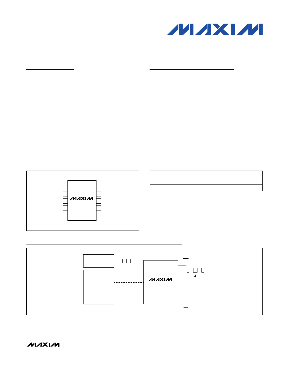
DS1124
5.0V 8-Bit Programmable
Timing Element
Rev 0; 7/07
+
Denotes a lead-free package.
Ordering Information
Pin Configuration
GND
OUT
V
CC
E
V
CC
IN
Q
CLK
D
MICROPROCESSOR
SYSTEM CLOCK
OPTIONAL
VARIABLE DELAY
DS1124
Typical Operating Circuit
________________________________________________________________
Maxim Integrated Products
1
For pricing, delivery, and ordering information, please contact Maxim Direct at 1-888-629-4642,
or visit Maxim’s website at www.maxim-ic.com.
TOP VIEW
+
IN
1
E
2
Q
3
DS1124
4
5
10
V
CC
V
9
CC
D
8
CLKGND
7
OUTGND
6
PART TEMP RANGE PIN-PACKAGE
DS1124U-25+ -40°C to +85°C 10 μSOP
DS1124U-25+T -40°C to +85°C 10 μSOP (Tape-and-Reel)
µSOP
ABSOLUTE MAXIMUM RATINGS
RECOMMENDED OPERATING CONDITIONS
(TA= -40°C to +85°C)
Stresses beyond those listed under “Absolute Maximum Ratings” may cause permanent damage to the device. These are stress ratings only, and functional
operation of the device at these or any other conditions beyond those indicated in the operational sections of the specifications is not implied. Exposure to
absolute maximum rating conditions for extended periods may affect device reliability.
Voltage Range on VCCPin Relative to Ground .....-0.5V to +6.0V
Voltage Range on IN, E, D, and CLK
Relative to Ground* ................................-0.5V to (V
CC
+ 0.5V)
Operating Temperature Range ...........................-40°C to +85°C
Storage Temperature Range .............................-55°C to +125°C
Short-Circuit Output Current ..........................50mA for 1 second
Soldering Temperature...................See J-STD-020 Specification
DC ELECTRICAL CHARACTERISTICS
(VCC= +4.75V to +5.25V, TA= -40°C to +85°C, unless otherwise noted.)
AC ELECTRICAL CHARACTERISTICS
(VCC= +4.75V to +5.25V, TA= -40°C to +85°C, unless otherwise noted.)
DS1124
5.0V 8-Bit Programmable
Timing Element
2 _______________________________________________________________________________________
*
Not to exceed +6.0V.
Supply Voltage V
Input Logic 1 V
Input Logic 0 V
PARAMETER SYMBOL CONDITIONS MIN TYP MAX UNITS
(Note 1) 4.75 5.25 V
CC
IH
IL
Active Current I
High-Level Output Current IOH V
Low-Leve l Output Current I
Input Leakage IL -1.0 +1.0 μA
PARAMETER SYMBOL CONDITIONS MIN TYP MAX UNITS
15 30 mA
CCA
= min, V
CC
Q pin, V
OL
OUT pin, V
2.2
-0.3 +0.8 V
= 2.3V -1.0 mA
OH
CC
CC
= min, V
= min, V
= 0.5V 4.0
OL
= 0.5V 8.0
OL
V
+
CC
0.3
V
mA
PARAMETER SYMBOL CONDITIONS MIN TYP MAX UNITS
Serial Clock Frequency f
Input Pulse Width (E, CLK) tEW, tCW 50 ns
Data Setup to C loc k t
Data Hold from Clock t
Data Setup to Enable t
Data Hold to Enable t
Enable Setup to Clock tES 0 ns
Enable Ho ld from Clock tEH 30 ns
E to Q Valid t
E to Q High Impedance t
CLK to Q Valid t
CLK to Q Invalid t
10 MHz
CLK
30 ns
DSC
0 ns
DHC
30 ns
DSE
0 ns
DHE
50 ns
EQV
0 50 ns
EQZ
50 ns
CQV
0 ns
CQX
DS1124
5.0V 8-Bit Programmable
Timing Element
_______________________________________________________________________________________ 3
Note 1: All voltages are referenced to ground.
Note 2: Measured from rising edge of the input to the rising edge of the output. The programmed delay, t
D
, can be programmed
with values from 0 to 255. See Figure 1.
Note 3: See the
Integral Nonlinearity
section and Figure 6.
Note 4: This is the minimum allowable interval between transitions on the input to ensure accurate device operation. This parameter
can be violated but timing accuracy may be impaired and ultimately very narrow pulse widths will result in no output from
the device. See Figure 1.
Note 5: When a 50% duty cycle input clock is used, this defines the highest usable clock frequency. When asymmetrical clock
inputs are used, the maximum usable clock frequency must be reduced to conform to the minimum input pulse-width
requirement. See Figure 1.
Note 6: Faster rise and fall times give the greatest accuracy in measured delay. Slow edges (outside the specification maximum)
can result in erratic operations.
AC ELECTRICAL CHARACTERISTICS (continued)
(VCC= +4.75V to +5.25V, TA= -40°C to +85°C, unless otherwise noted.)
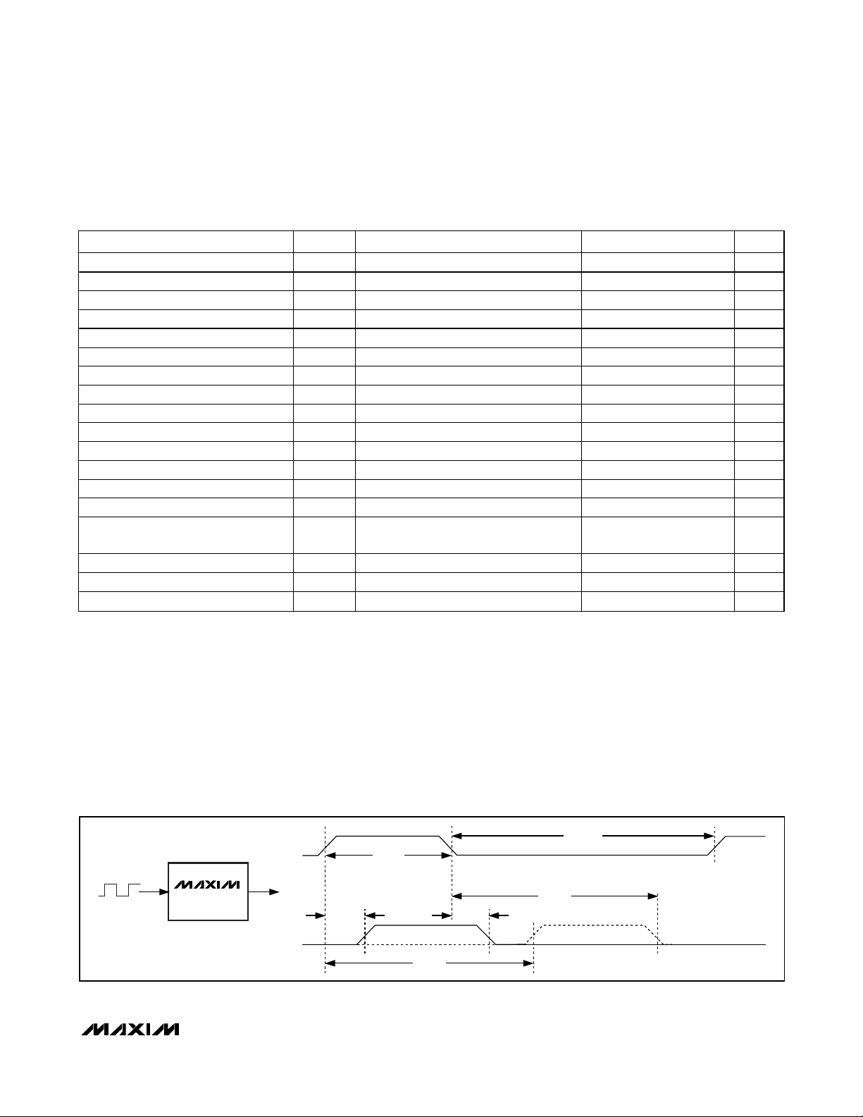
Figure 1. Delay Timing Diagram
E to Delay Val id t
E to Delay Invalid t
Power-Up Time tPU 100 ms
Delay Step Size t
Step 0 Delay TD0 (Note 2) 17 20 23 ns
Step 0 Delay Initial Accuracy VCC = 5V, TA = +25°C -0.6 +0.6 ns
Step 0 Voltage Variation -0.4 +0.4 ns
Step 0 Temperature Variation 0°C to +70°C -1 +1 ns
Step 0 Temperature Variation -40°C to +85°C -1 +1 ns
Step 255 Delay T
Step 255 Delay Initial Accuracy VCC = 5V, TA = +25°C -0.6 +0.6 ns
Step 255 Voltage Variat ion -0.4 +0.4 ns
Step 255 Temperature Variation 0°C to +70°C -3 +3 ns
Step 255 Temperature Variation -40°C to +85°C -5 +5 ns
Integral Nonlinearity
(Deviation from Straight Line)
Minimum Input Pulse Width tWI (Note 4) 40 ns
Minimum Input Period t
Input Ri se and Fall Times tR, tF (Note 6) 0 1 μs
PARAMETER SYMBOL CONDITIONS MIN TYP MAX UNITS
50 μs
EDV
0 ns
EDX
TA= +25°C -0.75 +0.25 +1 ns
STEP
(Note 2) 77 83.75 88 ns
D255
TA= +25°C (Note 3) -2 0 +2 ns
t
ERR
(Note 5) 80 ns
PER
t
WI
t
WI
t
D
D0
t
D0
t
D
IN
DS1124
TIMING REFERENCED TO 1.5V.
IN
OUT
t
OUT

DS1124
5.0V 8-Bit Programmable
Timing Element
Typical Operating Characteristics
(V
CC
= +5.0V, TA = +25°C, unless otherwise noted.)
4 _______________________________________________________________________________________
90
80
70
60
50
40
30
TYPICAL DELAY (ns)
20
10
0
0 250
ACTIVE SUPPLY CURRENT
20.0
19.5
19.0
18.5
18.0
17.5
ACTIVE SUPPLY CURRENT (mA)
17.0
16.5
1 100000
INPUT (IN) FREQUENCY (kHz)
vs. PROGRAMMED STEP
TYPICAL DELAY
PROGRAMMED STEP (dec)
vs. INPUT FREQUENCY
CHANGE FROM NOMINAL DELAY
vs. SUPPLY VOLTAGE
0.6
DS1124 toc01
0.4
STEP 255
0.2
0
STEP 0
-0.2
PROGRAMMED DELAY (ns)
-0.4
-0.6
225200150 17550 75 100 12525
4.75 5.25
SUPPLY VOLTAGE (V)
5.155.054.954.85
DS1124 toc02
PROGRAMMED DELAY (ns)
STANDBY SUPPLY CURRENT
vs. TEMPERATURE
25
VCC = 5.25V
DS1124 toc04
10000100010010
24
23
22
21
20
19
18
17
STANDBY SUPPLY CURRENT (mA)
16
15
-40
TEMPERATURE (°C)
DS1124 toc05
OUTPUT VOLTAGE (V)
806020 400-20
CHANGE FROM NOMINAL DELAY
vs. TEMPERATURE
2.0
1.5
1.0
0.5
-0.5
-1.0
-1.5
-2.0
STEP 255
0
STEP 0
-40
TEMPERATURE (°C)
DS1124 toc03
8060-20 0 20 40
OUTPUT VOLTAGE LOW
vs. OUTPUT CURRENT
0.30
VCC = 4.75V
0.25
0.20
0.15
0.10
0.05
0
010
OUTPUT CURRENT (mA)
8642
DS1124 toc06

DS1124
5.0V 8-Bit Programmable
Timing Element
_______________________________________________________________________________________ 5
Typical Operating Characteristics (continued)
(V
CC
= +5.0V, TA = +25°C, unless otherwise noted.)
Pin Description
PIN NAME FUNCTION
1 IN Delay Input Signal
2 E Input Enable
3 Q Serial Data Output
4, 5 GND Ground. Both grounds must be connected.
6 OUT Delay Output Signal
7 CLK Serial Clock Input
8 D Serial Data Input
9, 10 VCC Power Supply. Both supplies must be connected.
OUTPUT VOLTAGE HIGH
vs. OUTPUT CURRENT
DS1124 toc07
OUTPUT CURRENT (mA)
OUTPUT VOLTAGE (V)
-2-4-6-8
4.55
4.60
4.65
4.70
4.75
4.80
4.50
-10 0
DELAY INTEGRAL NONLINEARITY
vs. STEP
DS1124 toc08
STEP (dec)
DELAY INTEGRAL NONLINEARITY (ns)
250225200175150125100755025
-0.5
0
0.5
1.0
-1.0
0
DELAY DIFFERENTIAL NONLINEARITY
vs. STEP
DS1124 toc09
STEP (dec)
DELAY DIFFERENTIAL NONLINEARITY (ns)
250225200175150125100755025
-0.5
0
0.5
1.0
-1.0
0

DS1124
Detailed Description
The DS1124 is an 8-bit programmable delay line that
can be adjusted between 256 different delay intervals.
The DS1124 architecture (see Figure 2) allows some
signals to be delayed by more than one period, which
lets the phase of the signal to be adjusted up to a full
360°. Programming is performed by a 3-wire serial
interface. Using the 3-wire interface, it is possible to
cascade multiple devices together for systems requiring multiple programmable delays without using additional I/O resources.
Using the Serial Programming Interface
Serial mode operates similar to a shift register. When the
E pin is set at a high logic level, it enables the shift register and CLK clocks the data, D, into the register one bit at
a time starting with the most significant bit. After all 8 bits
are shifted into the DS1124, E must be pulled low to end
the data transfer and activate the new value. A settling
time (t
EDV
) is required after E is pulled low before the
signal delay will meet its specified accuracy. A timing
diagram for the serial interface is shown in Figure 3.
The 3-wire interface also has an output (Q) that can be
used to cascade multiple 3-wire devices, and it can be
used to read the current value of the devices on the
bus. To read the current values stored by the 3-wire
device(s), the latch must be enabled and the value of Q
must be read and then written back to D before the register is clocked. This causes the current value of the
register to be written back into the DS1124 as it is
being read. This can be accomplished in a couple of
different ways. If the microprocessor has an I/O pin that
is high impedance when set as an input, a feedback
resistor (R
FB
, generally between 1kΩ and 10kΩ) can be
used to write the data on Q back to D as the value is
read, see Figure 4A. If the microprocessor has an internal pullup on its I/O pins, or only offers separate input
and output pins, the value in the register can still be
read. The circuit shown in Figure 4B allows the Q values to read by the microprocessor, which must write
the Q value to D before it can clock the bus to read the
next bit. If the Q values are read without writing them to
D (with the pullup or otherwise), the read will be
destructive. A destructive read cycle likely results in an
undesirable change in the delay setting.
5.0V 8-Bit Programmable
Timing Element
6 _______________________________________________________________________________________
Block Diagram
Figure 2. Conceptual Design
IN
E
Q
CLK
D
PROGRAMMABLE
DELAY
8
8-BIT LATCH
8-BIT SHIFT
REGISTER
8
DS1124
OUT
IN OUT
t
256 CONTROL LINES
256 LINE DECODER
STEP
8-BIT LATCH VALUE
t
STEP
255 UNIT DELAY CELLS
t
STEP
t
STEP
DS1124

Figure 4C shows how to cascade multiple DS1124s onto
the same 3-wire bus. One important detail of writing
software for cascaded 3-wire devices is that all the
devices on the bus must be written to or read from
during each read or write cycle. Attempting to write to
only the first device (U1) would cause the data stored in
U1 to be shifted to U2, U2’s data would be shifted to U3,
etc. As shown, the microprocessor would have to shift
24 bits during each read or write cycle to avoid inadvertently changing the settings in any of the 3-wire devices.
Also note that the feedback resistor or a separate input
(not shown) can still be used to read the 3-wire device
settings when multiple devices are cascaded.
Integral Nonlinearity
Integral nonlinearity (INL) is defined as the deviation
from a straight line response drawn between the measured step zero delay (tD0) and the measured step 255
delay (t
D255
) with respect to the step 0 delay. Figure 5
shows INL’s effect on delay performance graphically.
Application Information
Power-Supply Decoupling
To achieve the best results when using the DS1124,
decouple the power supply with a 0.01µF and a 0.1µF
capacitor. Use high-quality, ceramic, surface mount
capacitors, and mount the capacitors as close as possible to the VCCand GND pins of the DS1124 to minimize
lead inductance. The DS1124 may not perform as specified if good decoupling practices are not followed.
DS1124
5.0V 8-Bit Programmable
Timing Element
_______________________________________________________________________________________ 7
ENABLE
Figure 3. Serial Interface Timing Diagram
CLOCK
(CLK)
t
EW
(E)
t
t
ES
t
CW
t
CW
EH
SERIAL
INPUT
SERIAL
OUTPUT
DELAY
TIME
t
DSC
(D)
t
EQV
(Q)
NEW BIT 7 NEW BIT 0
OLD BIT 7 OLD BIT 6 OLD BIT 0
t
DHC
NEW BIT 6
t
CQV t
PREVIOUS VALUE
t
CQX
t
EDX
EQZ
t
EDV
NEW VALUE

DS1124
Test Conditions
Input:
Ambient Temperature: 25°C ±3°C
Supply Voltage (VCC): 5.0V ±0.1V
Input Pulse: High = 3.0V ±0.1V
Low = 0.0V ±0.1V
Source Impedance: 50Ω max
Rise and Fall Times: 3.0ns max (measured
between 0.6V and 2.4V)
Pulse Width: 250ns
Period: 10µs
Output: The outputs are loaded with 15pF. Delay is
measured between the 1.5V level of the rising or falling
edge of the input signal and the corresponding edge of
the output signal.
Note: Above conditions are for test only and do not
restrict the operation of the device under other data
sheet conditions.
5.0V 8-Bit Programmable
Timing Element
8 _______________________________________________________________________________________
Figure 4. Examples Using the Serial Interface
C) CASCADING MULTIPLE DS1124s ON A 3-WIRE BUS.
MICROPROCESSOR
OUTPUT
I/O PIN
A) USING A FEEDBACK RESISTOR WITH AN I/O PIN FOR READING THE DS1124.
MICROPROCESSOR
OUTPUT
OUTPUT
I/O PIN
E
CLKOUTPUT
D
E
CLK
D
DS1124
R
FB
DS1124
U1
Q
Q
MICROPROCESSOR
OUTPUT
OUTPUT
INPUT
B) USING A SEPARATE INPUT PIN TO READ THE DS1124.
E
DS1124
U2
CLK
D
R
Q
FB
E
CLKOUTPUT
D
E
CLK
D
DS1124
Q
DS1124
U3
Q

DS1124
5.0V 8-Bit Programmable
Timing Element
Maxim cannot assume responsibility for use of any circuitry other than circuitry entirely embodied in a Maxim product. No circuit patent licenses are
implied. Maxim reserves the right to change the circuitry and specifications without notice at any time.
Maxim Integrated Products, 120 San Gabriel Drive, Sunnyvale, CA 94086 408-737-7600 _____________________
9
© 2007 Maxim Integrated Products is a registered trademark of Maxim Integrated Products, Inc.
DELAY
Figure 5. Integral Nonlinearity
Package Information
For the latest package outline information, go to
www.maxim-ic.com/DallasPackInfo
.
MEASURED t
MEASURED t
D255
D0
MEASURED DELAY
FOR ALL STEPS
EXAGGERATED
LINE FIT BETWEEN
MEASURED MAX
AND MIN DELAY
INL
255128 192640
STEP
 Loading...