

Page 1
DS1080CL
Spread-Spectrum Crystal Multiplier
________________________________________________________________
Maxim Integrated Products
1
Rev 0; 5/08
For pricing, delivery, and ordering information, please contact Maxim Direct at 1-888-629-4642,
or visit Maxim’s website at www.maxim-ic.com.
General Description
The DS1080CL is a low-jitter, crystal-based clock generator with an integrated phase-locked loop (PLL) to
generate spread-spectrum clock outputs from 8MHz to
64MHz. The device is pin programmable to select the
clock multiplier rate as well as the dither magnitude.
The DS1080CL has a spread-spectrum disable mode
and a power-down mode to conserve power.
Applications
Features
♦ Generates Spread-Spectrum Clocks from 8MHz to
64MHz
♦ Selectable Clock Multiplier Rates of 1x, 2x, and 4x
♦ Center Spread-Spectrum Dithering
♦ Selectable Spread-Spectrum Modulation
Magnitudes of ±0.5%, ±1.0%, and ±1.5%
♦ Spread-Spectrum Disable Mode
♦ Low Cycle-to-Cycle Jitter
♦ Power-Down Mode with High-Impedance Output
♦ Low Cost
♦ Low-Power Consumption
♦ 3.0V to 3.6V Single-Supply Operation
♦ -40°C to +125°C Temperature Operation
♦ Small 8-Pin µSOP Package
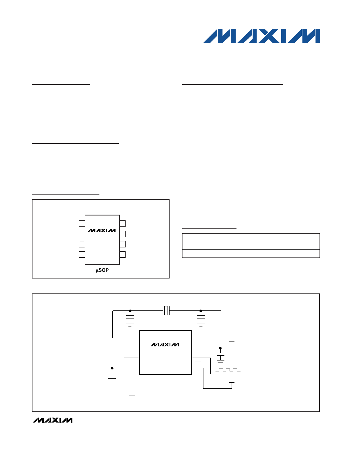
SSO
PDNSMSEL
1
2
87X2
V
CC
GND
CMSEL
X1
TOP VIEW
3
4
6
5
DS1080CL
+
Pin Configuration
+
Denotes a lead-free package.
T = Tape and reel.
Ordering Information
Automotive
Cable Modems
Cell Phones
Computer Peripherals
Copiers
Infotainment
PCs
Printers
X2
NOTE: IN THE ABOVE CONFIGURATION WITH PDN CONNECTED TO VCC, SMSEL CONNECTED TO GND, AND CMSEL FLOATING, THE DEVICE IS IN NORMAL
OPERATION WITH 2x CLOCK MULTIPLICATION AND A SPREAD-SPECTRUM MAGNITUDE OF ±0.5%.
f
SSO
V
CC
V
CC
V
CC
SSO
PDN
X1
CRYSTAL
C
L1
C
L2
DECOUPLING
CAPACITOR
GND
CMSEL
SMSEL
8
7
6
5
1
2
3
4
DS1080CL
Typical Operating Circuit
PART TEMP RANGE PIN-PACKAGE
DS1080CLU+ -40°C to +125°C 8 μSOP
DS1080CLU+T -40°C to +125°C 8 μSOP
Page 2
DS1080CL
Spread-Spectrum Crystal Multiplier
2 _______________________________________________________________________________________
ABSOLUTE MAXIMUM RATINGS
RECOMMENDED OPERATING CONDITIONS
(TA= -40°C to +125°C.)
Stresses beyond those listed under “Absolute Maximum Ratings” may cause permanent damage to the device. These are stress ratings only, and functional
operation of the device at these or any other conditions beyond those indicated in the operational sections of the specifications is not implied. Exposure to
absolute maximum rating conditions for extended periods may affect device reliability.
Voltage Range on VCCRelative to GND .............-0.5V to +3.63V
Voltage Range on Any Pin Relative
to GND ...............-0.5V to (V
CC
+ 0.5V), not to exceed +3.63V
Operating Temperature Range .........................-40°C to +125°C
Storage Temperature Range .............................-55°C to +125°C
Soldering Temperature...........................Refer to the IPC/JEDEC
J-STD-020 Specification.
DC ELECTRICAL CHARACTERISTICS
(VCC= +3.0V to +3.6V, TA= -40°C to +125°C.)
PARAMETER SYMBOL CONDITIONS MIN TYP MAX UNITS
Supply Voltage VCC (Note 1) 3.0 3.6 V
Input Logic 1 V
Input Logic 0 V
Input Logic Float IIF 0V < VIN < V
Input Leakage IIL 0V < VIN < V
SSO Load C
Crystal or Clock Input
Frequency
Crystal ESR X
Cloc k Input Duty Cycle F
Crystal Parallel Load
Capacitance
IH
IL
15 pF
SSO
f
8 16 MHz
IN
90
ESR
40 60 %
INDC
C
(Note 4) 18 pF
L
0.8 x
V
CC
GND -
0.3
(Note 2) ±1 μA
CC
(Note 3) ±80 μA
CC
VCC +
0.3
0.2 x
V
CC
V
V
PARAMETER SYMBOL CONDITIONS MIN TYP MA X UNITS
Supply Current I
Power-Down Current I
Output Leakage (SSO) I
Low-Leve l Output Voltage
(SSO)
High-Level Output Voltage
(SSO)
Input Capacitance (X1/X2) CIN (Note 5) 5 pF
C
CC1
CCQ
OZ
V
IOL = 4mA 0.4 V
OL
V
IOH = -4mA 2.4 V
OH
= 15pF, SSO = 8MHz 7 12 mA
SSO
PDN = GND, all input pins floating 200 μA
PDN = GND -1 +1 μA
Page 3

DS1080CL
Spread-Spectrum Crystal Multiplier
_______________________________________________________________________________________ 3
AC ELECTRICAL CHARACTERISTICS
(VCC= +3.0 to +3.6V, TA= -40°C to +125°C.)
Note 1: All voltages referenced to ground.
Note 2: Maximum source/sink current applied to input to be considered a float.
Note 3: Applicable to pins CMSEL, SMSEL, and PDN.
Note 4: See information about C
L1
and CL2in the
Applications Information
section.
Note 5: Not production tested.
Note 6: For 15pF load.
Note 7: Time between PDN deasserted to output active.
Note 8: Time between PDN asserted to output high impedance.
Note 9: Guaranteed by design.
PARAMETER SYMBOL CONDITIONS MIN TYP MA X UNITS
SSO Duty C yc le SSODC Measured at VCC/2 45 55 %
Rise Time tR (Note 6) 1.6 ns
Fal l Time tF (Note 6) 1.6 ns
f
= 8MHz, TA = -40°C to +85°C,
Peak Cycle-to-Cycle Jitter t
Power-Up Time t
Power-Down Time t
Dither Rate f
DITHER
J
POR
PDN
SSO
10,000 cyc les (Note 5)
PDN pin (Note 7)
PDN pin (Notes 8, 9) 100 ns
fIN/512
8MHz 20
16MHz 10
75 ps
ms
Page 4
DS1080CL
Spread-Spectrum Crystal Multiplier
4 _______________________________________________________________________________________
Typical Operating Characteristics
(VCC= 3.3V, TA = +25°C, unless otherwise noted.)
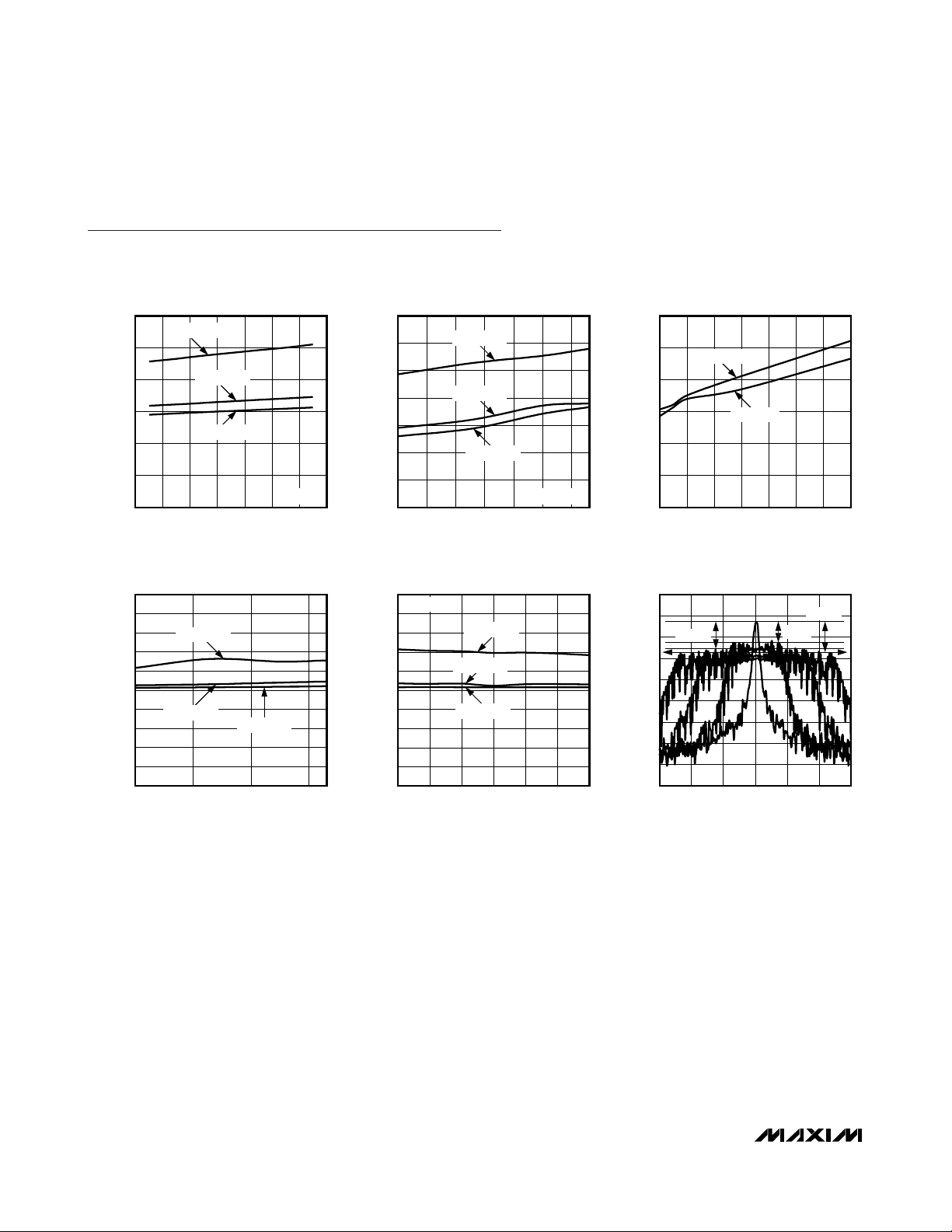
SUPPLY CURRENT vs. SUPPLY VOLTAGE
DS1080CL toc01
SUPPLY VOLTAGE (V)
SUPPLY CURRENT (mA)
3.553.453.353.253.153.05
2
4
6
8
10
12
0
2.95 3.65
fIN = 8MHz
CMSEL = 4x
CMSEL = 2x
CMSEL = 1x
SUPPLY CURRENT vs. TEMPRATURE
DS1080CL toc02
TEMPERATURE (°C)
SUPPLY CURRENT (mA)
11085603510-15
2
4
6
8
10
12
14
0
-40
fIN = 8MHz
CMSEL = 4x
CMSEL = 2x
CMSEL = 1x
SUPPLY CURRENT vs. FREQUENCY
DS1080CL toc03
FREQUENCY (MHz)
SUPPLY CURRENT (mA)
564840322416
2
4
6
8
10
12
0
864
VCC = 3.6V
VCC = 3.0V
DUTY CYCLE vs. TEMPERATURE
DS1080CL toc04
TEMPERATURE (°C)
DUTY CYCLE (%)
1106010
46
47
48
49
50
51
52
53
54
55
45
-40
CMSEL = 4x
CMSEL = 2x
fIN = 8MHz
CMSEL = 1x
DUTY CYCLE vs. SUPPLY VOLTAGE
DS1080CL toc05
SUPPLY VOLTAGE (V)
DUTY CYCLE (%)
3.53.43.33.23.1
46
47
48
49
50
51
52
53
54
55
45
3.0 3.6
CMSEL = 4x
CMSEL = 2x
fIN = 8MHz
CMSEL = 1x
FREQUENCY SPECTRUM AT 64MHz
DS1080CL toc06
FREQUENCY (MHz)
ATTENUATION (dB)
6665646362
-80
-70
-60
-50
-40
-30
-20
-10
0
-90
61 67
-11dB
-15.6dB
-14.1dB
Page 5

DS1080CL
Spread-Spectrum Crystal Multiplier
_______________________________________________________________________________________ 5
Block Diagram
Pin Description
PIN NAME FUNCTION
1 X1
Crystal Drive/Clock Input. A cr ystal with the proper loading capacitors is connected across X1 and X2.
Instead of a crystal, a clock can be applied at the X1 input.
2 GND Signal Ground
3 CMSEL
Clock Multiplier Select. Trilevel digital input.
0 = 1x
Float = 2x
1 = 4x
4 SMSEL
Spread-Spectrum Magnitude Select. Trilevel digital input.
0 = ±0.5%
Float = ±1.0%
1 = ±1.5%
5 PDN
Power-Down/Spread-Spectrum Disable. Trilevel digital input.
0 = Power-Down/SSO High Impedance
Float = Power-Up/Spread Spectrum Disabled
1 = Power-Up/Spread Spectrum Enab led
6 SSO
Spread-Spectrum Clock Multipl ier Output. Outputs a 1 x, 2x, or 4x spread-spectrum version of the crysta l
or clock applied at the X1/X2 pins.
7 VCC Supply Voltage
8 X2
Crystal Drive Output. A crystal with the proper loading capacitors is connected across X1 and X2.
If a clock is connected to X1, then X2 should be left open circuit.
f
8MHz
TO
16MHz
C
C
L2
L1
CMSEL
SMSEL
IN
X1
CRYSTAL
X2
OSCILLATOR
CONFIGURATION DECODE
AND CONTROL
1x/2x/4x CLOCK MULTIPLYING
PLL WITH SPREAD SPECTRUM
NOTE: SEE INFORMATION ABOUT CL1 AND CL2 IN THE APPLICATIONS INFORMATION SECTION.
DS1080CL
V
CC
V
CC
f
SSO
f
SSO
PDN
GND
SSO
64MHz
= 8MHz
TO
Page 6

DS1080CL
Spread-Spectrum Crystal Multiplier
6 _______________________________________________________________________________________
Detailed Description
The DS1080CL is a crystal multiplier with center
spread-spectrum capability. An 8MHz to 16MHz crystal
is connected to the X1 and X2 pins. Alternately, an
8MHz to 16MHz clock can be applied to X1 in place of
the crystal. In such applications, X2 would be left open
circuit. Using the CMSEL input, the user selects
whether the attached crystal or input clock is multiplied
by 1, 2, or 4. The DS1080CL can generate spreadspectrum clocks from 8MHz to 64MHz.
The PLL can dither the output clock about its center frequency at a user-selectable magnitude. Using the
SMSEL input, the user selects the dither magnitude.
The PDN input can be used to place the device into a
low-power standby mode where the SSO output is high
impedance. If the PDN pin is floated, the SSO output is
active but the spread-spectrum dithering is disabled.
The spread-spectrum dither rate is fixed at f
IN
/512 to
keep the dither rate above the audio frequency range.
On power-up, the output clock (SSO) remains high
impedance until the PLL reaches a stable frequency
(f
SSO
) and dither (f
DITHER
). A power cycle is needed
for the PLL whenever there is a change in input frequency, CMSEL, or SMSEL.
Figure 1. Spread-Spectrum Frequency Modulation
SSO
+1.5%
f
+1.0%
+0.5%
f
O
-0.5%
-1.0%
-1.5%
DITHER CYCLE RATE = f
= fIN/512
DITHER
t
Page 7

DS1080CL
Spread-Spectrum Crystal Multiplier
Maxim cannot assume responsibility for use of any circuitry other than circuitry entirely embodied in a Maxim product. No circuit patent licenses are
implied. Maxim reserves the right to change the circuitry and specifications without notice at any time.
Maxim Integrated Products, 120 San Gabriel Drive, Sunnyvale, CA 94086 408-737-7600 _____________________
7
© 2008 Maxim Integrated Products is a registered trademark of Maxim Integrated Products, Inc.
Applications Information
Crystal Selection
The DS1080CL requires a parallel resonating crystal
operating in the fundamental mode, with an ESR of less
than 90Ω. The crystal should be placed very close to
the device to minimize excessive loading due to parasitic capacitances.
Oscillator Input
When driving the DS1080CL using an external oscillator
clock, consider the input (X1) to be high impedance.
Crystal Capacitor Selection
The load capacitors CL1and CL2are selected based
on the crystal specifications (from the data sheet of the
crystal used). The crystal parallel load capacitance is
calculated as follows:
For the DS1080CL use CL1= CL2= CLX.
In this case, the equation then reduces to:
where CL1= CL2= C
LX.
Equation 2 is used to calculate the values of CL1and
CL2based on values of CLand CINnoted in the electrical specifications.
Power-Supply Decoupling
To achieve best results, it is highly recommended that
a decoupling capacitor is used on the IC power-supply
pins. Typical values of decoupling capacitors are
0.001μF and 0.1μF. Use a high-quality, ceramic, surface-mount capacitor, and mount it as close as possible to the VCCand GND pins of the IC to minimize lead
inductance.
Layout Considerations
As noted earlier, the crystal should be placed very
close to the device to minimize excessive loading due
to parasitic capacitances. Care should also be taken to
minimize loading on pins that could be floated as a programming option (SMSEL and CMSEL). Coupling on
inputs due to clocks should be minimized.
(2)
(1)
Package Information
For the latest package outline information and land patterns, go
to www.maxim-ic.com/packages
.
PACKAGE TYPE PACKAGE CODE DOCUMENT NO.
8 μSOP —
21-0036
CxC
12
C
LL
=
L
CC
LL
C
=+
L
C
2
LX
+
C
IN
+
12
C
IN
 Loading...