

Datasheet DS1075Z-80, DS1075Z-66, DS1075Z-60, DS1075Z-100, DS1075M-80 Datasheet (Dallas Semiconductor)
...Page 1
r
www.maxim-ic.com.com
2
3
4
DS1075
EconOscillator/Divide
FEATURES
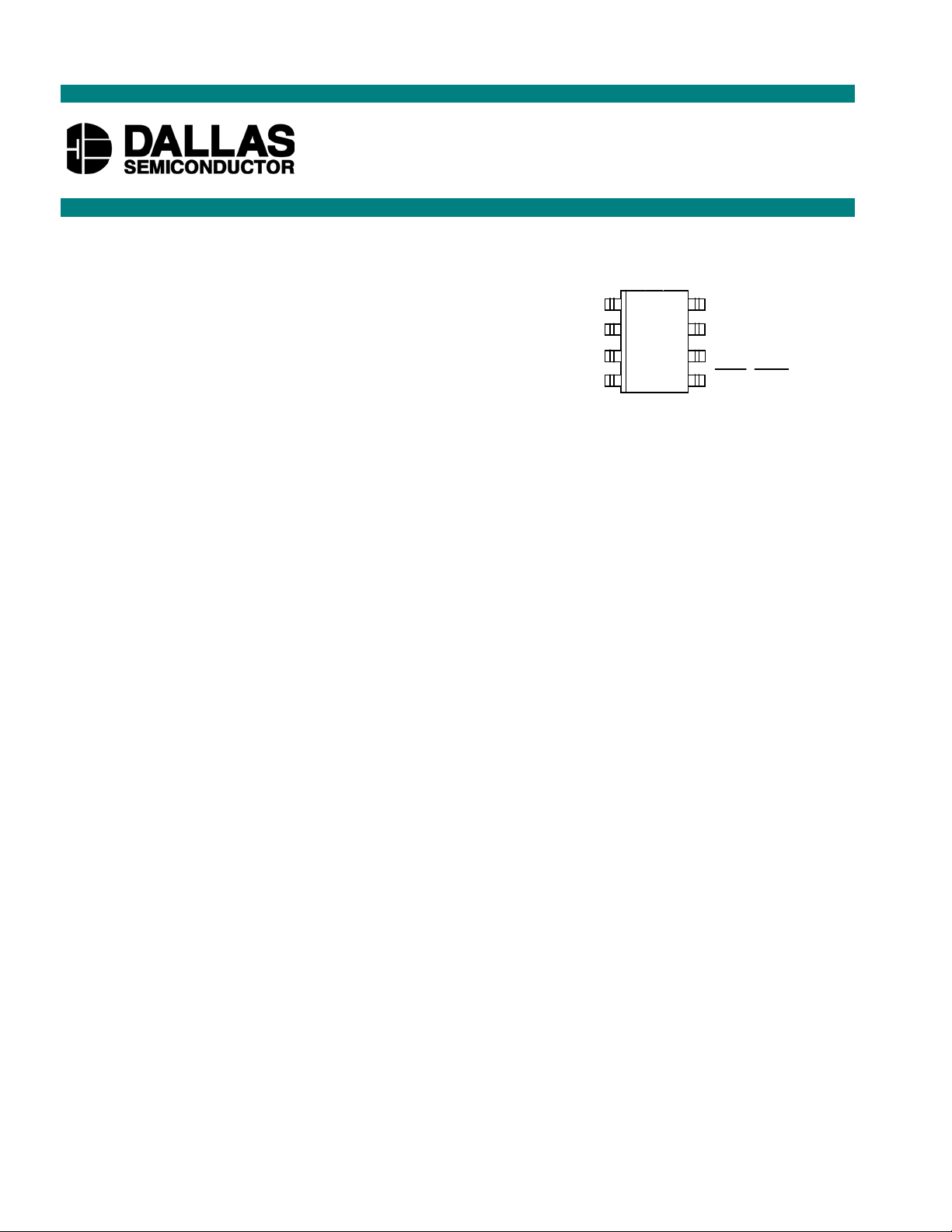
PIN ASSIGNMENT
§ Dual Fixed frequency outputs
1
8
7
6
5
OSCIN
XTAL
OE
PDN/SELX
(30 KHz - 100 MHz)
§ User-programmable on-chip dividers
(from 1 - 513)
§ User-programmable on-chip prescaler
(1, 2, 4)
§ No external components
I/O
OUT0
V
GND
DS1075Z 150-MIL SOIC
DS1075M 300-MIL DIP
§ ±0.5% Initial tolerance
§ ±1% variation over temperature and voltage
§ Internal clock, External clock or crystal
reference options
§ Single 5V supply
§ Power-down mode
§ Synchronous output gating
FREQUENCY OPTIONS
Part No. Max O/P freq.
DS1075-100 100.000 MHz
DS1075-80 80.000 MHz
DS1075-66 66.667 MHz
DS1075-60 60.000 MHz
DESCRIPTION
The DS1075 is a fixed frequency oscillator requiring no external components for operation. Numerous
operating frequencies are possible in the range of approximately 30 KHz to 100 MHz through the use of
an on-chip programmable prescaler and divider.
The DS1075 features a master oscillator followed by a prescaler and then a programmable divider. The
prescaler and programmable divider are user-programmable with the desired values being stored in
nonvolatile memory. This allows the user to buy an off the shelf component and program it on site prior
to board production. Design changes can be readily accommodated by programming, or reprogramming,
the desired values into the on-chip nonvolatile registers. Evaluation boards, DS1075K and DS1070K are
available to simplify this task.
The DS1075 is shipped from the factory configured for half the maximum operating frequency. Contact
the factory for specially programmed devices. As alternatives to the on-board oscillator an external clock
signal or a crystal may be used as a reference. The choice of reference source (internal or external) is
user-selectable at the time of programming (or on the fly if the SEL mode is chosen).
The DS1075 features a dual-purpose Input/Output pin. If the device is powered up in Program mode this
pin can be used to input serial data to the on-chip registers. After a Write command this data is stored in
nonvolatile memory. When the chip is subsequently powered up in operating mode these values are
automatically restored to the on-chip registers and the Input/Output pin becomes the oscillator output.
The DS1075 is available in 8-pin DIP or SOIC packages, allowing the generation of a clock signal easily,
economically and using minimal board area.
1 of 18 100899
Page 2
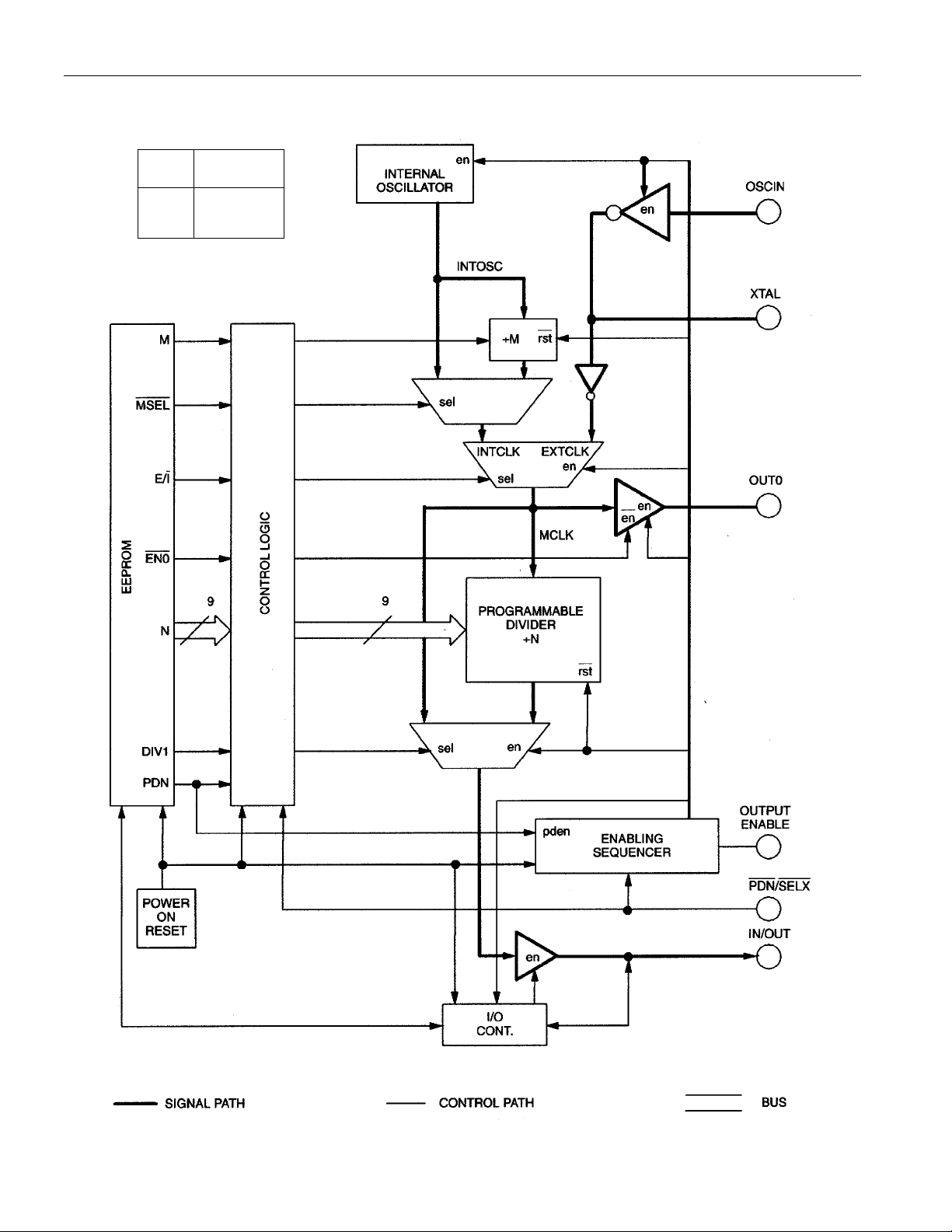
BLOCK DIAGRAM Figure 1
DS1075
PART
NO.
SUFFIX
-100
080
-66
-60
INTOSC
FREQUENCY
100.000 MHz
80.000 MHz
66.667 MHz
60.000 MHz
2 of 18
Page 3

DS1075
PIN DESCRIPTIONS
Input/Output Pin (IN/OUT): This pin is the main oscillator output, with a frequency determined by clock
reference, M and N dividers. Except in programming mode this pin is always an output and will be
referred to as “OUT”. In programming mode this pin will be referred to as “IN”.
External Oscillator Input (OSCIN): This pin can be used to supply an external reference frequency to
the device.
Crystal Oscillator Connection (XTAL): A crystal can be connected between this pin and OSCIN to
provide an alternative frequency reference. If a crystal is not used this pin should be left open.
Output Enable Function (OE pin): The DS1075 also features a “synchronous” output enable. When
OE is at a high logic level the oscillator free runs. When this pin is taken low OUT is held low,
immediately if OUT is already low, or at it’s next high-to-low transition if OUT is high. This prevents
any possible truncation of the output pulse width when the enable is used. While the output is disabled
the master oscillator continues to run (producing an output at OUT0, if the EN0 bit = 0) but the internal
counters (/N) are reset. This results in a constant phase relationship between OE’s return to a high level
and the resulting OUT signal. When the enable is released OUT will make its first transition within one
to two clock periods of the master clock.
Power-Down/Select Function ( PDN /SELX PDN/SELX pin): The Power-Down/Select ( PDN /SELX ) pin
has a user-selectable function determined by one bit ( PDN bit) of the user-programmable memory.
According to which function is selected, this pin will be referred to as PDN or SELX .
If the Power-Down function is selected (PDN bit = 1) a low logic level on this pin can be used to make
the device stop oscillating (active low) and go into a reduced power consumption state. The “Enabling
Sequencer” circuitry will first disable OUT in the same way as when OE is used. Next OUT0 will be
disabled in a similar fashion. Finally the oscillator circuitry will be disabled. In this mode both outputs
will go into a high impedance state. The power consumption in the power-down state is much less than if
OE is used because the internal oscillator (if used) is completely powered down. Even if an external
reference or a crystal is used all of the on-chip buffers are powered down to minimize current drain.
Consequently the device will take considerably longer to recover (i.e., achieve stable oscillation) from a
power-down condition than if the OE is used.
If the Select function is chosen (PDN bit = 0) this pin can be used to switch between the internal
oscillator and an external reference (or crystal) on the fly. When this mode is chosen the E/
overridden, a high logic level on
SELX will select the internal oscillator, a low logic level will select the
I select bit is
external reference (or crystal oscillator).
Reference Output (OUT0 pin): A reference output, OUT0, is also available from the output of the
reference select mux. This output is especially useful as a buffered output of a crystal defined master
frequency. OUT0 is unaffected by the OE pin, but is disabled in a glitchless fashion if the device is
powered down. If this output is not required it can be permanently disabled by setting the
EN0 bit to one,
and there will be a corresponding reduction in overall power consumption.
USER-PROGRAMMABLE REGISTERS
The following registers can be programmed by the user to determine operating frequency and mode of
operation. Details of how these registers are programmed can be found in a later section, in this section
3 of 18
Page 4
DS1075
the function of the registers are described. The register settings are nonvolatile, the values being stored
automatically in EEPROM when the registers are programmed.
Note: The register bits cannot be used to make mode or frequency changes on the fly. Changes can only
be made by powering the device up in “Programming” mode. For them to be become effective the device
must then be powered down and powered up again in “Operation” mode.
For programming purposes the register bits are divided into two 9-bit words, the “MUX” word
determines mode of operation and prescaler values. The “DIV” word sets the value of the programmable
divider.
MUX WORD Figure 2
(MSB) (LSB)
0* 0* 0*
EN0
PDN M
MSEL
DIV1
E/ I
* These bits must be set to zero
E/I
This bit selects either the internal oscillator or the external/ crystal reference.
1=External/Crystal
0=Internal Oscillator
however, if the PDN bit is set to zero the E/I bit will be overridden by the logic level on the
PDN / SELX pin.
Table 1
PDN
BIT E/ I
0 X 0 EXTERNAL/CRYSTAL
0 X 1 INTERNAL
1 X 0 POWER-DOWN
1 0 1 INTERNAL
1 1 1 EXTERNAL/CRYSTAL
PDN /SELX
PIN
OSCILLATOR
MODE
DIV1
This bit allows the master clock to be routed directly to the output (DIV1=1). The N programmable
divider is bypassed so the programmed value of N is ignored. The frequency of the output (f
) will be
OUT
INTCLK or EXTCLK depending on which reference has been selected. If the Internal clock is selected
the M prescaler is also bypassed (the bit values of MSEL and M are ignored) so in this case f
OUT
=INTOSC (which also equals MCLK and INTCLK). If DIV1=0 the prescaler and programmable divider
function normally.
MSEL
This bit determines whether or not the M prescaler is bypassed. MSEL =1 will bypass the prescaler.
MSEL =0 will switch in the prescaler (unless overridden by DIV1=1), with a divide-by number
determined by the M bit.
M
This bit sets the divide-by number for the prescaler. M=0 results in divide-by-4, M=1 results in divideby-2. The setting of this bit is irrelevant if either DIV1=1 or MSEL =1.
4 of 18
Page 5

DS1075
Table 2
DIV1
BIT
E/ I
BIT*
0000INTERNAL OSCILLATOR DIVIDED BY 4*N
0001INTERNAL OSCILLATOR DIVIDED BY 2*N
0 0 1 X INTERNAL OSCILLATOR DIVIDED BY N
0 1 X X EXTERNAL OSCILLATOR DIVIDED BY N
1 0 X X INTERNAL OSCILLATOR DIVIDED BY 1
1 1 X X EXTERNAL OSCILLATOR DIVIDED BY 1
*Assuming PDN bit = 1, otherwise internal/external selection will be controlled by the PDN / SELX pin.
MSEL
BIT
M
BIT OPERATION
DIV WORD Figure 3
(MSB) (LSB)
N (9-BITS)
PDN
This bit is used to determine the function of the PDN / SELX pin. If PDN=0, the PDN / SELX pin can be
used to determine the timing reference (either the internal oscillator or an external reference/crystal). If
PDN=1, the PDN / SELX pin is used to put the device into power-down mode.
EN0
This bit is used to determine whether the OUT0 pin is active or not. If EN0 =1, OUT0 is disabled (Highimpedance). If EN0 =0, the internal reference clock (MCLK) is output from OUT0. The OE pin has no
effect on OUT0, but OUT0 is disabled as part of the power-down sequence.
N
These nine bits determine the value of the programmable divider. The range of divisor values is from 2 to
513, and is equal to the programmed value of N plus 2:
Table 3
BIT
VALUES
000000000 2
000000001 3
..
..
..
..
..
111111111 513
DIVISOR (N)
VALUE
NOTE:
The maximum value of N is constrained by the minimum output frequency. If the internal clock is
selected, INTOSC/(M*N) must be greater than f
be greater than f
. (If DIV1=1, then INTOSC or EXTCLK, as applicable, must exceed f
OUTmin
; if the external clock is selected, EXTCLK/N must
OUTmin
5 of 18
OUTmin
).
Page 6
DS1075
OPERATION OF OUTPUT ENABLE
Since the output enable, internal master oscillator and/or external master oscillator are likely all
asynchronous there is the possibility of timing difficulties in the application. To minimize these
difficulties the DS1075 features an “enabling sequencer” to produce predictable results when the device is
enabled and disabled. In particular the output gating is configured so that truncated output pulses can
never be produced.
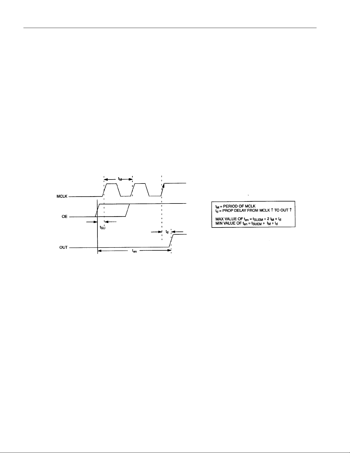
ENABLE TIMING
The output enable function is produced by sampling the OE input with the output from the prescaler mux
(MCLK) and gating this with the output from the programmable divider. The exact behavior of the
device is therefore dependent on the setup time (t
of MCLK. If the actual setup time is less than t
) from a transition on the OE input to the rising edge
SU
then one more complete cycle of MCLK will be
SUEM
required to complete the enable or disable operation (see diagrams). This is unlikely to be of any
consequence in most applications, and then only if the value for N is small. In general, the output will
make its first positive transition between approximately one and two clock periods of MCLK after the
rising edge of OE.
FIGURE 4
DISABLE TIMING
If OE goes low while OUT is high, the output will be disabled on the completion of the output pulse. If
OUT is low, the disabling behavior will be dependent on the setup time between the falling edge of OE
and the rising edge of MCLK. If t
output before disabling occurs. If the device is in divide-by-one mode, the disabling occurs slightly
differently. In this case if t
SU
> t
additional output pulses will appear.
The following diagrams illustrate the timing in each of these cases.
< t
SU
one additional output pulse will appear, if tSU < t
SUEM
the result will be one additional pulse appearing on the
SUEM
SUEM
then two
6 of 18
Page 7

Figure 5
Figure 6
DS1075
SELECT TIMING
If the PDN bit is set to “0”, the PDN / SELX pin can be used to switch between the internal oscillator and
an externalor crystal reference. The “Enabling Sequencer” is again employed to ensure this transition
occurs in a glitch-free fashion. Two asynchronous clock signals are involved, INTCLK is the internal
reference oscillator divided by one or whatever value of M is selected. EXTCLK is the clock signal fed
into the OSCIN pin, or the clock resulting from a crystal connected between OSCIN and XTAL. The
behavior of OUT0 is described in the following paragraphs, the OUT pin will behavior similarly but will
be divided by N.
FROM INTERNAL TO EXTERNAL CLOCK
This is accomplished by a high to low transition on the SELX pin. This transaction is detected on the
falling edge of INTCLK. The output OUT0 will be held low for a minimum of half the period of
INTCLK (t
switching will not occur until EXTCLK returns to a low level.
/2), then if EXTCLK is low it will be routed through to OUT0. If EXTCLK is high the
I
7 of 18
Page 8

DS1075
Figure 7
Depending on the relative timing of the SELX signal and the internal clock, there may be up to one full
cycle of t
pulses will be dependent on the relative timing between t
edge of SELX and the first rising edge of the externally derived clock is t
minimum values of these parameters are:
on the output after the falling edge of SELX . Then, the “low” time (t
I
and t
I
. The time interval between the falling
E
. Approximate maximum and
SIE
) between output
LOW
(min) = t
t
LOW
t
(max) = t
LOW
t
(min) = t
SIE
t
(max) = 3 t
SIE
I
/2
I
/2
/2 + t
I
/2 + t
I
E
E
NOTE:
In each case there will be a small additional delay due to internal propagation delays.
FROM EXTERNAL TO INTERNAL CLOCK
This is accomplished by a low to high transition on the SELX pin. In this case the switch is level
triggered, to allow for the possibility of a clock signal not being present at OSCIN. Note therefore, that if
a constant high-level signal is applied to OSCIN it will not be possible to switch over to the internal
reference. (Level triggering was not employed for the switch from internal to external reference as this
approach is slower and the internal clock may be running at a much higher frequency than the maximum
allowed external clock rate). When SELX is high and a low level is sensed on EXTCLK, OUT0 will be
held low until a falling edge occurs on INTCLK, then the next rising edge of INTCLK will be routed
through to OUT0.
Figure 8
Depending on the relative timing of the SELX signal and the external clock, there may be up to one full t
high period on the output after the rising edge of SELX . Then, the “low” time (t
pulses will be dependent on the relative timing between t
and tE. The time interval between the falling
I
) between output
LOW
8 of 18
E
Page 9

DS1075
edge of SELX and the first rising edge of the externally derived clock is t SIE . Approximate maximum
and minimum values of these parameters are:
t
(min) = t
LOW
t
(max) = 3t
LOW
t
(min) = t
SIE
t
(max) = 3 t
SIE
/2
I
/2
I
I
/2 + t
I
/2 + t
Elow
Ehigh
NOTE:
In each case there will be a small additional delay due to internal propagation delays.
POWER-DOWN CONTROL
If the PDN bit is set to “1”, the PDN / SELX pin can be used to power-down the device. If PDN is high
the device will run normally.
POWER-DOWN
If PDN is taken low a power-down sequence is initiated. The “Enabling Sequencer” is used to execute
events in the following sequence:
1. Disable OUT (same sequence as when OE is used) and reset N counters.
2. When OUT is low, switch OUT to high-impedance state.
3. Disable MCLK (and OUT0 if EN0 bit = 0), switch OUT0 to high impedance state.
4. Disable internal oscillator and OSCIN buffer.
POWER-UP
When PDN is taken to a high level the following power-up sequence occurs:
1. Enable internal oscillator and/or OSCIN buffer.
2. Set M and N to maximum values.
3. Wait approximately 256 cycles of MCLK for it to stabilize.
4. Reset M and N to programmed values.
5. Enable OUT0 (assuming
6. Enable OUT.
Steps 2 through 4 exist to allow the oscillator to stabilize before enabling the outputs.
EN0 bit = 0).
9 of 18
Page 10

DS1075
Figure 9
POWER-ON RESET
When power is initially applied to the device supply pin, a power-on reset sequence is executed, similar
to that which occurs when the device is restored from a power-down condition. This sequence comprises
two stages, first a conventional POR to initialize all on-chip circuitry, followed by a stabilization period
to allow the oscillator to reach a stable frequency before enabling the outputs:
1. Initialize internal circuitry.
2. Enable internal oscillator and/or OSCIN buffer.
3. Set M and N to maximum values.
4. Wait approximately 256 cycles of MCLK for the oscillator to stabilize.
5. Load M and N programmed values from EEPROM.
6. Enable OUT0 (assuming EN0=0).
7. Enable OUT.
Figure 10
PROGRAMMING
Normally when power is applied to the supply voltage pin the device will enter its normal operating mode
following the power-on reset sequence. However the device can be made to enter a programming mode if
a pull-up resistor is connected between IN/OUT and the supply voltage pin, prior to power-up. The
method used for programming is a variant of the 1-Wire
Semiconductor products.
™ protocol used on a number of Dallas
10 of 18
Page 11

DS1075
HARDWARE
The hardware configuration is shown in the diagram. A bus master is used to read and write data to the
DS1075’s internal registers. The bus master may have either an open-drain or TTL-type architecture.
Figure 11
Programming mode is entered by simply powering up the DS1075 with a pull-up of approximately 5KW.
This will pull the IN/OUT pin above V
DS1075 to internally release the IN/OUT pin (after t
on power-up and initiate the programming mode, causing the
IH
), and allow the pull-up resistor to pull the pin to
POR
the supply rail and await the Master Tx Reset pulse (see diagram).
NOTE:
To ensure normal operation any external pull-up applied to IN/OUT must be greater than 20KW in value.
This will cause the IN/OUT pin to remain below V
end of t
STAB
.
on power-up, resulting in normal operation at the
IH
Figure 12
11 of 18
Page 12

DS1075
TRANSACTION SEQUENCE
The sequence for accessing the DS1075 via the 1-Wire port is as follows:
Initialization
Function Command
Transaction/Data
INITIALIZATION
All transactions on the 1-Wire bus begin with an initialization sequence. The initialization sequence
consists of a reset pulse transmitted by the bus master followed by a presence pulse(s) transmitted by the
DS1075. The presence pulse lets the bus master know that the DS1075 is present and is ready to operate.
Figure 13
FUNCTION COMMANDS
Once the bus master has detected a presence, it can issue one of the four function commands. All
Function Commands are eight bits long, and are written lsb first. A list of these commands follows:
Write DIV Register [01H]
This command allows the bus master to write to the DS1075’s DIV register.
Read DIV Register [A1H]
This command allows the bus master to read the DS1075’s DIV register.
Write MUX Register [02H]
This command allows the bus master to write to the DS1075’s MUX register.
Read MUX Register [A2H]
This command allows the bus master to read the DS1075’s MUX register.
TRANSACTION/DATA
Immediately following the Function Command, the nine data bits are written to or read from the DS1075.
This data is written/read lsb first. The following diagrams illustrate the timing. Once data transfer is
complete a new transaction sequence can be started by re-initializing the device. Therefore to program
both the DIV and MUX registers two complete transaction sequences are required.
12 of 18
Page 13

DS1075
READ/WRITE TIME SLOTS
The definitions of write and read time slots are illustrated below. All time slots are initiated by the master
driving the data line low. The falling edge of the data line synchronizes the DS1075 to the master by
triggering a delay circuit in the DS1075. During write time slots, the delay circuit determines when the
DS1075 will sample the data line. For a read data time slot, if a “0” is to be transmitted, the delay circuit
determines how long the DS1075 will hold the data line low overriding the 1 generated by the master. If
the data bit is a “1”, the DS1075 will leave the read data time slot unchanged.
WRITE “1” TIME SLOT Figure 14
WRITE “0” TIME SLOT Figure 15
13 of 18
Page 14

DS1075
READ DATA TIME SLOT Figure 16
RETURN TO NORMAL OPERATION
When programming is complete the DS1075 should be powered down. If the pullup resistor on the
IN/OUT pin is removed, normal device operation will be restored next time power is applied.
DEFAULT REGISTER VALUES
Unless ordered from the factory with specific register program values, the DS1075 is shipped with the
following default register values:
DIV = 0 0000 0000 (Programmable divider will divide by two)
MUX = 0 0011 0100
OUT0 Disabled
Power-Down Enabled, Select Disabled
M = 4 (Ignored, see MSEL )
MSEL = 1 (M prescaler bypassed)
DIV1 = 0 (N Dividers enabled)
E/ I = 0 (Internal oscillator selected)
14 of 18
Page 15

DS1075
ABSOLUTE MAXIMUM RATINGS*
Voltage on Any Pin Relative to Ground -1.0V to +7.0V
Operating Temperature 0°C to 70°C
Storage Temperature -55°C to +125°C
Soldering Temperature 260°C for 10 seconds
* This is a stress rating only and functional operation of the device at these or any other conditions above
those indicated in the operation sections of this specification is not implied. Exposure to absolute
maximum rating conditions for extended periods of time may affect reliability.
DC ELECTRICAL CHARACTERISTICS (TA = 0°C to 70°C, VCC = 5V + 5%)
PARAMETER SYMBOL CONDITION MIN TYP MAX UNITS NOTES
Supply Voltage V
High-level Output
Voltage
V
(IN/OUT, OUT0)
Low-level Output
Voltage
V
(IN/OUT, OUT0)
High-level Input Voltage
( PDN /SELX , OE,
IN/OUT)(OSCIN)
Low-level Input
Voltage( PDN /SELX ,
OE, IN/OUT)(OSCIN)
High-level Input Current
( PDN /SELX , OE,
IN/OUT)(OSCIN)
Low-level Input Current
( PDN /SELX , OE,
IN/OUT)(OSCIN)
Supply Current (Active)
DS1075-100
DS1075-80
DS1075-66
DS1075-60
Standby Current
I
(power-down)
V
V
V
V
I
IH
I
IH
I
IL
I
IL
I
CC
CCQ
CC
OH
OL
IH
IH
IL
IL
IOH = -4 mA,
VCC = MIN
IOL = 4 mA 0.4 V
VIH =2.4V, VCC=
5.25V V
IH
=VCC =5.25V
VIL =0,VCC=
5.25V V
IL
=0,VCC =5.25V
CL = 15 pF
(both outputs)
Power-down
Mode
4.75 5 5.25 V
2.4 V
2
3
0.8
2
V
V
V
V
125
uA
uA
-1
-25
uA
uA
35 50 mA
0.8 uA
15 of 18
Page 16

DS1075
AC ELECTRICAL CHARACTERISTICS (TA = 0°C to 70°C, VCC = 5V + 5%)
PARAMETER SYMBOL CONDITION MIN TYP MAX UNITS NOTES
Output Frequency
Df
O
Tolerance
Combined Freq.
Df
O
Variation
Long Term Stability
Frequency
Minimum Output
Df
f
OSCIN
f
OUT
O
Frequency
Power-Up Time t
Enable OUT from PDN ↑
Enable OUT0 from
PDN ↑
OUT Hi-Z from PDN ↓
OUT0 Hi-Z from PDN ↓
Load Capacitance
por
+ t
t
stab
t
stab
t
pdn
t
pdn
C
stab
L
(IN/OUT, OUT0)
Output Duty Cycle
IN/OUT, OUT0
Jitter J 100 pS 7
VCC = 5V, TA =
-0.5 0 +0.5 %
25°C
Over temp and
-1 +1 %
voltage
-0.5 +0.5 %
External clock 50 MHzMaximum Input
Crystal reference 25 MHz
29.3 kHz 2
0.1 1 ms 3, 4
0.1 1 ms 4
0.1 1 ms 4, 5
1ms
1ms
15 pF 6
40
40
60
60
%
%
1
NOTES:
1. This is the maximum frequency which can be applied to OSCIN, or, the maximum crystal frequency
that can be used.
2. The values of M, N and the frequency of OSCIN (if used) must be chosen so that this spec is met.
3. This is the time from when VCC is applied until the output starts oscillating.
4. When the device is initially powered up, or restored from the power-down mode, OE should be
asserted (high). Otherwise the start of the t
subsequently be returned to a low level during the t
If the external mode is selected t
will be a function of the OSCIN period, i.e., external clock
stab
frequency. See “Calculated Parameters” to determine the value of t
5. Although OE does not normally affect OUT0 operation, if OE is held low during power-up the start of
the t
period will be delayed until OE is asserted. If OE remains low, OUT0 will not start.
stab
6. Operation with higher capacitive loads is possible but may impair output voltage swing and maximum
operation frequency.
7. Parameter given is a typical max.
interval will be delayed until OE goes high. OE can
stab
interval to force out low after the t
stab
in this case.
stab
interval.
stab
16 of 18
Page 17

DS1075
AC ELECTRICAL CHARACTERISTICS - CALCULATED PARAMETERS
The following characteristic are derived from various device operating parameters (frequency, mode etc.).
They are not specifically tested or guaranteed and may differ from the min and max limits shown by a
small amount due to internal device setup times and propagation delays. However, the equations in the
max column can be used to estimate a more accurate idea of typical device performance than the
guaranteed values.
PARAMETER SYMBOL CONDITION MIN MAX
OUT ↑= from OE ↑=
OUT ↓O from OE ↓
t
en
t
distdis
N = 1
N ≥ 2
SELX ↓ to OUT0 ↑
t
SIEtSEI
-Internal to External
-External to Internal
Break during SEL switch
t
LOWtLOW
-Internal to External
-External to Internal
PDN ↓to IN/OUT Hi-Z
t
pdntpdn
N = 1
N ≥ 2
PDN ↓to OUT0 Hi-Z
t
pdntpdn
N = 1
N ≥ 2
PDN ↑ = to OUT↑ =
PDN ↑ = to OUT0 ↑=
t
t
stab
stab
OUT↑ = after Power-Up
OUT0↑ after Power-Up 256t
t
M
t
OUTH
0
tI /2
tI /2
tI /2
tI /2
t
OUTH
0
t
OUTH
0
2t
M
t
+ t
OUTH
t
OUTH
3tI /2 + t
3tI /2 + t
tI /2 + t
3tI /2 + t
t
+ t
OUTH
t
OUTH
t
+ t
OUTH
t
OUTH
256t
256t
256t
M
E
Ehigh
E
Elow
M
M
M
M
M
M
17 of 18
Page 18

DS1075
DATA SHEET REVISION SUMMARY
The following represent the key differences between 11/16/97 and 05/01/97 version of the DS1075 data
sheet. Please review this summary carefully.
1. Page 1, description, second paragraph. Word change
2. Page 14, AC electrical characteristic. Add Long Term Stability and new spec.
The following represent the key differences between 05/01/97 and 10/15/97 version of the DS1075 data
sheet. Please review this summary carefully.
1. Status Change (REMOVE PRELIMINARY).
18 of 18
 Loading...