

Page 1
g
n
OUT3
OUT7OU
6
查询DS1007供应商
www.dalsemi.com
DS1007
7-1 Silicon Delay Line
FEATURES
All-silicon time delay
7 independent buffered delays
Delay tolerance ±2 ns
Four delays can be custom set between 3 ns
and 10 ns
Three delays can be custom set between 9 ns
and 40 ns
Delays are stable and precise
Economical
Auto-insertable, low profile
Surface mount 16-pin SOIC
Low-power CMOS
TTL/CMOS-compatible
Vapor phase, IR and wave solderable
Custom specifications available
Quick turn prototypes
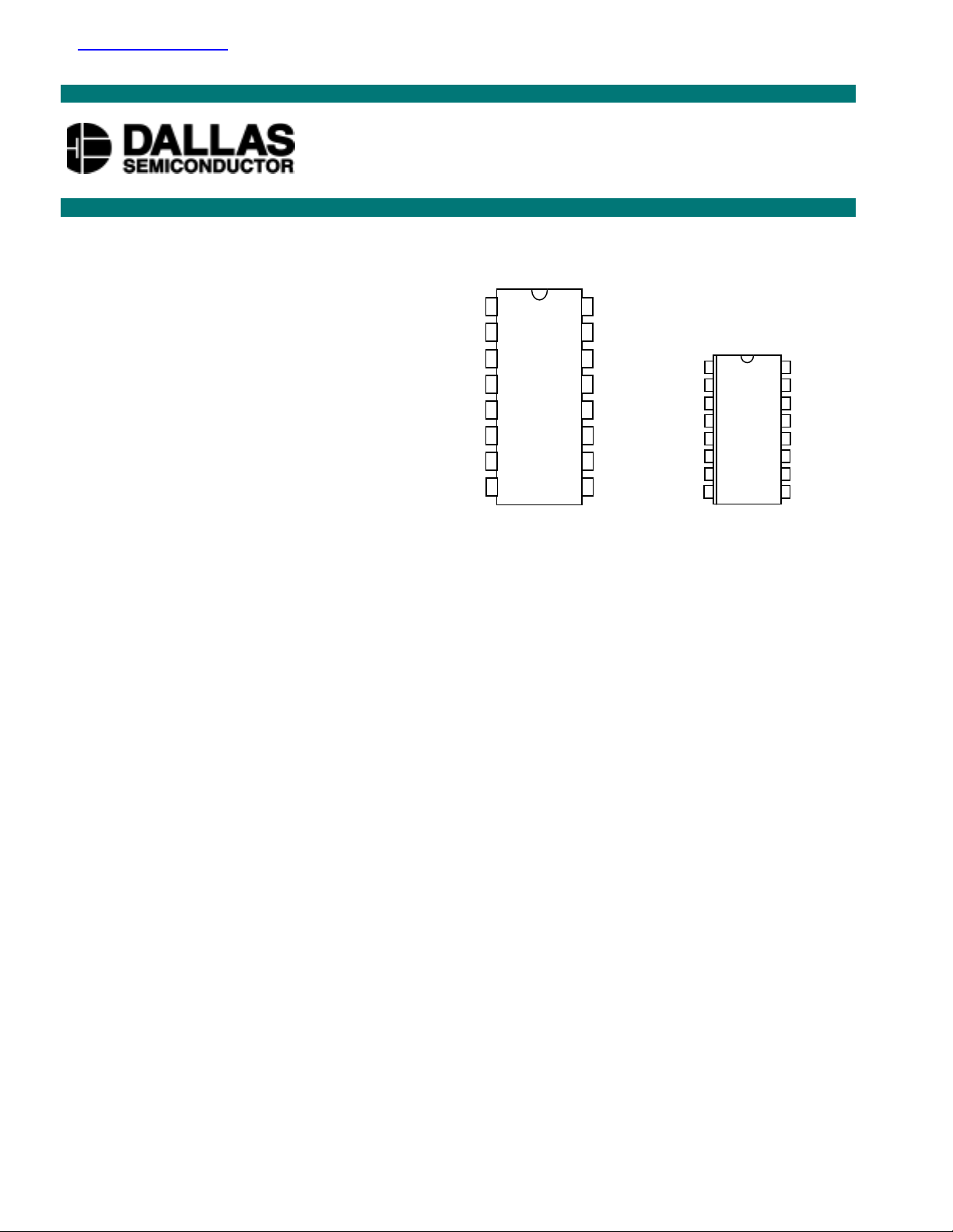
PIN ASSIGNMENT
IN1
OUT1
OUT2
OUT5
IN2
V
IN5
IN6
2
3
4
CC
5
6
7
8
DS1007 16-Pin DIP (300-mil)
See Mech. Drawings Section
14
16
15
13
12
11
10
IN31
OUT3
IN4
OUT4
GND
OUT7
IN7
9
OUT6
PIN DESCRIPTION
IN1 - IN7 - Inputs
Out1 – Out7 - Outputs
GND - Ground
V
CC
- +5 Volts
IN1
1
16
OUT1
IN2
OUT2
V
IN5
OUT5
IN6
CC
15
2
14
3
4
13
5
12
11
7
10
8
9
DS1007S 16-Pin SOIC
(300-mil)
See Mech. Drawin
IN3
IN4
T4
GND
OUT6
s Sectio
DESCRIPTION
The DS1007 7-in-1 Silicon Delay Line provides seven independent delay times which are set by Dallas
Semiconductor to the customer’s specification. The delay times can be set from 3 ns to 40 ns with an
accuracy of ±2 ns at room temperature. The device is offered in both a 16-pin DIP and a 16-pin SOIC.
Since the DS1007 is an all-silicon solution, better economy and reliability are achieved when compared to
older methods using hybrid technology. The DS1007 reproduces the input logic state at the output after
the fixed delay. Dallas Semiconductor can customize standard products to meet special needs. For special
requests and rapid delivery, call (972) 371–4348.
1 of 6 111799
Page 2
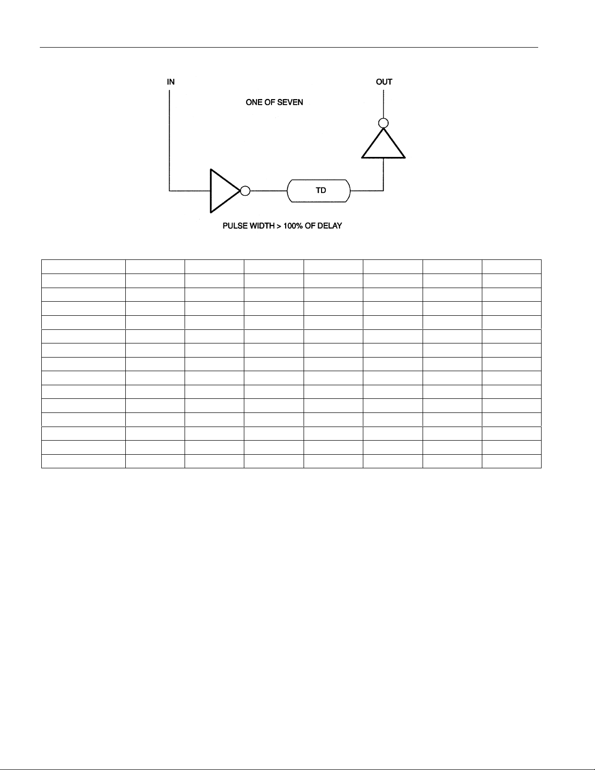
LOGIC DIAGRAM Figure 1
DS1007
PART NUMBER DELAY TABLE (t
PART # OUT1 OUT2 OUT3 OUT4 OUT5 OUT6 OUT7
DS1007-1 3ns 4ns 5ns 6ns 9ns 13ns 18ns
DS1007-2 4 6 8 10 12 14 16
DS1007-3 3333101010
DS1007-4 4444121212
DS1007-5 5555151515
DS1007-6 6666202020
DS1007-7 7777252525
DS1007-8 8888303030
DS1007-9 9999353535
DS1007-10 10 10 10 10 40 40 40
DS1007-11 3468101214
DS1007-12 3468101520
DS1007-13 3468121520
DS1007-14 7777999
Custom delays available. Out 1 through Out 4 can be custom set from 3 to 10 ns (leading edge only
accuracy). Out 5 through Out 7 can be set from 9 to 40 ns (both leading and trailing edge accuracy).
) Table 1
PLH
2 of 6
Page 3
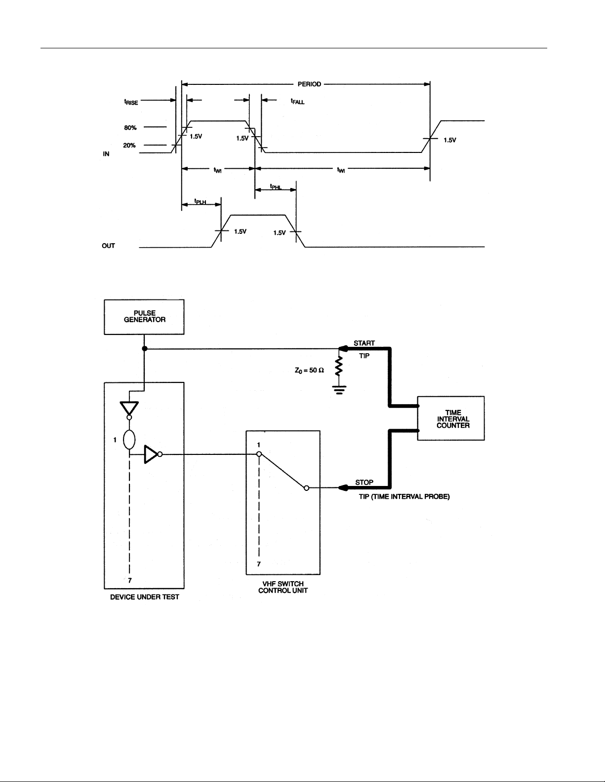
TIMING DIAGRAM: SILICON DELAY LINE Figure 2
TEST CIRCUIT Figure 3
DS1007
3 of 6
Page 4
DS1007
ABSOLUTE MAXIMUM RATINGS*
Voltage on Any Pin Relative to Ground -1.0V to +7.0V
Operating Temperature 0°C to 70°C
Storage Temperature -55°C to +125°C
Soldering Temperature 260°C for 10 seconds
Short Circuit Output Current 50 mA for 1 second
* This is a stress rating only and functional operation of the device at these or any other conditions above
those indicated in the operation sections of this specification is not implied. Exposure to absolute
maximum rating conditions for extended periods of time may affect reliability.
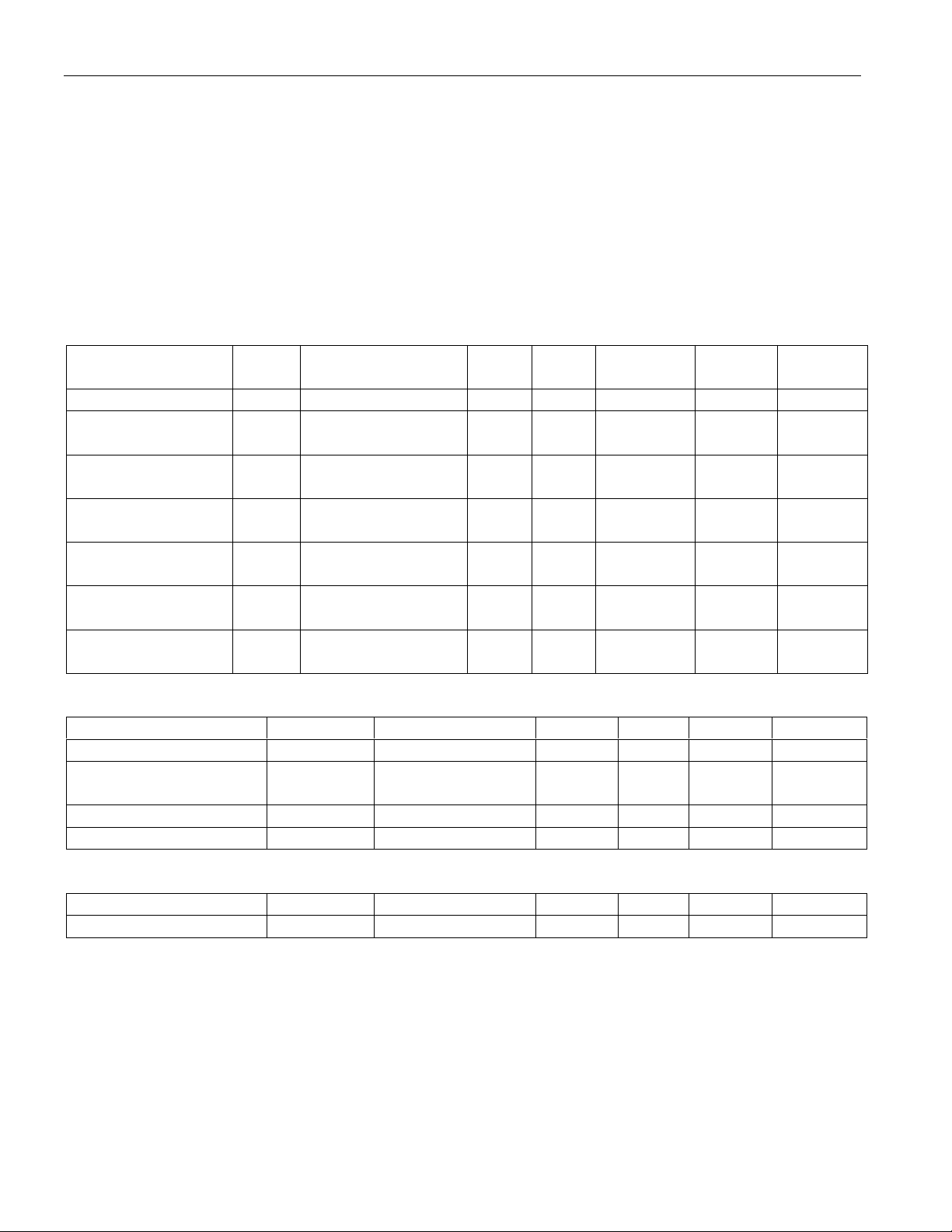
DC ELECTRICAL CHARACTERISTICS (0°C to 70°C; VCC = 5.0V ± 5%)
PARAMETER SYM TEST
CONDITION
Supply Voltage V
High Level Input
V
CC
IH
Voltage
Low Level Input
V
IL
Voltage
Input Leakage
I
I
0.0V ≤ VI ≤ V
Current
Active Current I
CC
VCC=Max;
Period=Min.
High Level Output
Current
Low Level Output
Current
I
OH
VCC=Min.
VOH=2.4V
I
OL
VCC=Min.
VOL=0.5V
CC
MIN TYP MAX UNITS NOTES
4.75 5.00 5.25 V 1
2.2 VCC + 0.5 V 1
-0.5 0.8 V 1
-1.0 1.0 uA
40.0 70.0 mA 2
-1.0 mA
12.0 mA
AC ELECTR ICAL CHARACTERISTICS (TA = 25°C; VCC = 5V ± 5%)
PARAMETER SYMBOL MIN TYP MAX UNITS NOTES
Input Pulse Width t
Input to Output
t
PLH
WI
100% of t
PLH
ns
Table 1 ns 3, 4, 5
(leading edge)
Power-up Time t
PU
100 ms 7
Period 3 (tWI)ns6
CAPACITANCE (TA = 25°C)
PARAMETER SYMBOL MIN TYP MAX UNITS NOTES
Input Capacitance C
IN
510pF
4 of 6
Page 5

DS1007
NOTES:
1. All voltages are referenced to ground.
2. Measured with outputs open.
3. VCC = 5V @25°C. Delays accurate on rising edges within ±2 ns.
4. See Test Conditions below.
5. All output delays in the same speed output tend to vary unidirectionally with temperature or voltage
range (i.e., if Out 2 slows down, all other outputs also slow down).
6. Period specifications may be exceeded; however, accuracy will be application-sensitive (decoupling,
layout, etc.).
7. tPU = 0 ms for Out 1 through Out 4.
TERMINOLOGY
Period: The time elapsed between the leading edge of the first pulse and the leading edge of the
following pulse.
tWI (Pulse Width): The elapsed time on the pulse between the 1.5V point on the leading edge and the
1.5V point on the trailing edge, or the 1.5V point on the trailing edge and the 1.5 V point on the leading
edge.
t
(Input Rise Time): The elapsed time between the 20% and the 80% point on the leading edge of the
RISE
input pulse.
t
(Input Fall Time): The elapsed time between the 80% and the 20% point on the trailing edge of the
FALL
input pulse.
t
(Time Delay, Rising): The elapsed time between the 1.5V point on the leading edge of the input
PLH
pulse and the 1.5V point on the leading edge of the corresponding output pulse.
TEST SETUP DESCRIPTION
Figure 3 illustrates the hardware configuration used for measuring the timing parameters on the DS1007.
The input waveform is produced by a precision pulse generator under software control. Time delays are
measured by a time interval counter (20 ps resolution) connected between the input and each output. Each
output is selected and connected to the counter by a VHF switch control unit. All measurements are fully
automated, with each instrument controlled by a central computer over an IEEE 488 bus.
5 of 6
Page 6

DS1007
TEST CONDITIONS
INPUT:
Ambient Temperature: 25°C ± 3°C
Supply Voltage (VCC): 5.0V ± 0.1V
Input Pulse: High = 3.0V ± 0.1V
Low = 0.0V ± 0.1V
Source Impedance: 50 ohm max.
Rise and Fall Time: 3.0 ns max.
Pulse Width: 500 ns
Period: 1 µs
OUTPUT:
Each output is loaded with the equivalent of one 74F04 input gate. Delay is measured at the 1.5V level on
the rising edge.
NOTE:
Above conditions are for test only and do not restrict the operation of the device under other data sheet
conditions.
6 of 6
 Loading...