

Datasheet DRV135UA-2K5, DRV135UA, DRV134UA-1K, DRV134UA, DRV134PA Datasheet (Burr Brown Corporation)
Page 1
®
DRV134
DRV134
DRV134
AUDIO BALANCED LINE DRIVERS
FEATURES
● BALANCED OUTPUT
● LOW DISTORTION: 0.0005% at f = 1kHz
● WIDE OUTPUT SWING: 17Vrms into 600Ω
● HIGH CAPACITIVE LOAD DRIVE
● HIGH SLEW RATE: 15V/µs
● WIDE SUPPLY RANGE: ±4.5V to ±18V
● LOW QUIESCENT CURRENT: ±5.2mA
● 8-PIN DIP, SO-8, AND SOL-16 PACKAGES
● COMPANION TO AUDIO DIFFERENTIAL
LINE RECEIVERS: INA134 and INA137
● IMPROVED REPLACEMENT FOR SSM2142
APPLICATIONS
● AUDIO DIFFERENTIAL LINE DRIVER
● AUDIO MIX CONSOLES
● DISTRIBUTION AMPLIFIER
● GRAPHIC/PARAMETRIC EQUALIZERS
● DYNAMIC RANGE PROCESSORS
● DIGITAL EFFECTS PROCESSORS
● TELECOM SYSTEMS
● HI-FI EQUIPMENT
● INDUSTRIAL INSTRUMENTATION
DRV135
DRV135
DESCRIPTION
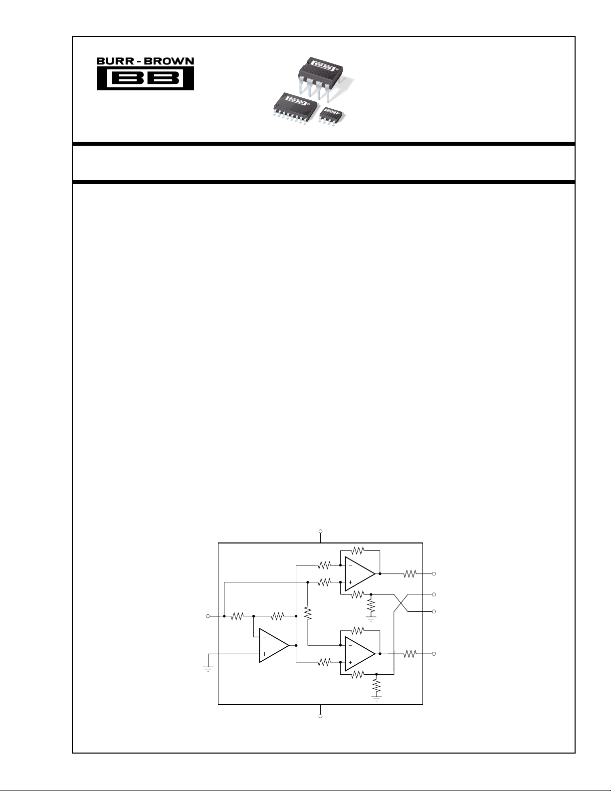
The DRV134 and DRV135 are differential output
amplifiers that convert a single-ended input to a
balanced output pair. These balanced audio drivers
consist of high performance op amps with on-chip
precision resistors. They are fully specified for high
performance audio applications and have excellent
ac specifications, including low distortion (0.0005%
at 1kHz) and high slew rate (15V/µs).
The on-chip resistors are laser-trimmed for accurate
gain and optimum output common-mode rejection. Wide
output voltage swing and high output drive capability
allow use in a wide variety of demanding applications.
They easily drive the large capacitive loads associated
with long audio cables. Used in combination with the
INA134 or INA137 differential receivers, they offer a
complete solution for transmitting analog audio signals
without degradation.
The DRV134 is available in 8-pin DIP and SOL-16
surface-mount packages. The DRV135 comes in a
space-saving SO-8 surface-mount package. Both are
specified for operation over the extended industrial
temperature range, –40°C to +85°C and operate from
–55°C to +125°C.
V+
A2
V
IN
Gnd
All resistors 30kΩ unless otherwise indicated.
International Airport Industrial Park • Mailing Address: PO Box 11400, Tucson, AZ 85734 • Street Address: 6730 S. Tucson Blvd., Tucson, AZ 85706 • Tel: (520) 746-1111 • Twx: 910-952-1111
Internet: http://www.burr-brown.com/ • FAXLine: (800) 548-6133 (US/Canada Only) • Cable: BBRCORP • Telex: 066-6491 • FAX: (520) 889-1510 • Immediate Product Info: (800) 548-6132
©1998 Burr-Brown Corporation PDS-1451A Printed in U.S.A. October, 1998
A1
A3
V–
50Ω
10kΩ
50Ω
10kΩ
+V
O
+Sense
–Sense
–V
O
Page 2
SPECIFICATIONS: V
= ±18V
S
At TA = +25°C, VS = ±18V, RL = 600Ω differential connected between +VO and –VO, unless otherwise noted.
DRV134PA, UA
DRV135UA
PARAMETER CONDITIONS MIN TYP MAX UNITS
AUDIO PERFORMANCE
Total Harmonic Distortion + Noise THD+N f = 20Hz to 20kHz,VO = 10Vrms 0.001 %
Noise Floor, RTO
Headroom, RTO
INPUT
Input Impedance
Input Current I
(1)
(1)
(2)
Z
IN
IN
GAIN [(+V
Differential VIN = ±10V
f = 1kHz, V
= 10Vrms 0.0005 %
O
20kHz BW –98 dBu
THD+N < 1% +27 dBu
10 kΩ
VIN = ±7.07V ±700 ±1000 µA
) – (–VO)]/V
O
IN
Initial 5.8 6 dB
Error ±0.1 ±2%
vs Temperature ±10 ppm/°C
Single-Ended V
= ±5V
IN
Initial 5.8 6 dB
Error ±0.7 ±2%
vs Temperature ±10 ppm/°C
Nonlinearity 0.0003 % of FS
OUTPUT
Common-Mode Rejection, f = 1kHz OCMR See OCMR Test Circuit, Figure 4 46 68 dB
Signal Balance Ratio, f = 1kHz SBR See SBR Test Circuit, Figure 5 35 54 dB
Output Offset Voltage
Offset Voltage, Common-Mode V
vs Temperature ±150 µV/°C
Offset Voltage, Differential V
OCM
(3)
(4)
OD
VIN = 0 ±50 ±250 mV
VIN = 0 ±1 ±10 mV
vs Temperature ±5 µV/°C
vs Power Supply PSRR V
Output Voltage Swing, Positive No Load
Negative No Load
= ±4.5V to ±18V 80 110 dB
S
(5)
(5)
(V+) – 3 (V+) – 2.5 V
(V–) + 2 (V–) + 1.5 V
Impedance 50 Ω
Load Capacitance, Stable Operation C
Short-Circuit Current I
Tied to Ground (each output) 1 µF
LCL
SC
±85 mA
FREQUENCY RESPONSE
Small-Signal Bandwidth 1.5 MHz
Slew Rate SR 15 V/µs
Settling Time: 0.01% V
= 10V Step 2.5 µs
OUT
Overload Recovery Output Overdriven 10% 3 µs
POWER SUPPLY
Rated Voltage V
S
±18 V
Voltage Range ±4.5 ±18 V
Quiescent Current I
Q
IO = 0 ±5.2 ±5.5 mA
TEMPERATURE RANGE
Specification Range –40 +85 °C
Operation Range –55 +125 °C
Storage Range –55 +125 °C
Thermal Resistance
8-Pin DIP 100 °C/W
θ
JA
SO-8 Surface Mount 150 °C/W
SOL-16 Surface Mount 80 °C/W
NOTES: (1) dBu = 20log (Vrms/0.7746). (2) Resistors are ratio matched but have ±20% absolute value. (3) V
(5) Guarantees linear operation. Includes common-mode offset.
= [(+VO) + (–VO)]/2. (4) VOD = (+VO) – (–VO).
OCM
The information provided herein is believed to be reliable; however, BURR-BROWN assumes no responsibility for inaccuracies or omissions. BURR-BROWN assumes
no responsibility for the use of this information, and all use of such information shall be entirely at the user’s own risk. Prices and specifications are subject to change
without notice. No patent rights or licenses to any of the circuits described herein are implied or granted to any third party. BURR-BROWN does not authorize or warrant
any BURR-BROWN product for use in life support devices and/or systems.
®
DRV134, 135
2
Page 3
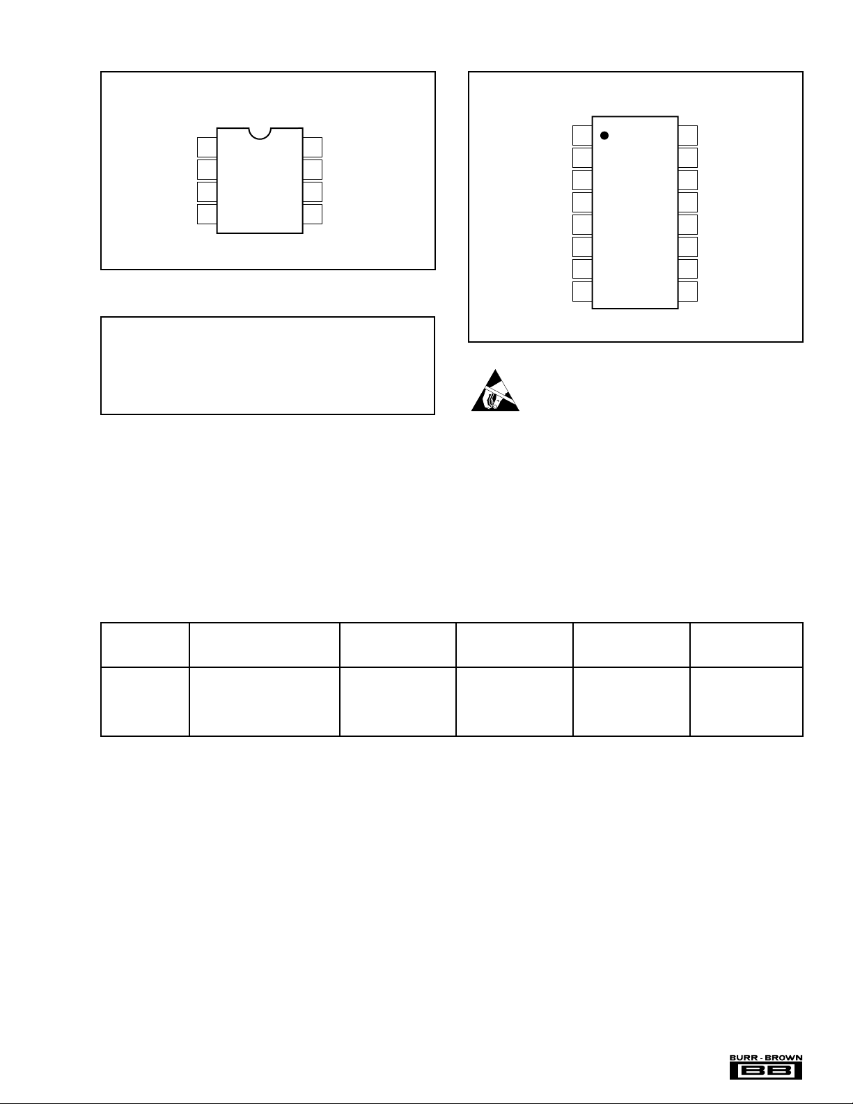
PIN CONFIGURATIONS
Top View 8-Pin DIP/SO-8
–V
1
O
Gnd
V
2
3
4
IN
–Sense
ABSOLUTE MAXIMUM RATINGS
Supply Voltage, V+ to V– .................................................................... 40V
Input Voltage Range .................................................................... V– to V+
Output Short-Circuit (to ground) .............................................. Continuous
Operating Temperature .................................................. –55°C to +125°C
Storage Temperature ..................................................... –55°C to +125°C
Junction Temperature .................................................................... +150°C
Lead Temperature (soldering, 10s) ............................................... +300°C
NOTE: (1) Stresses above these ratings may cause permanent damage.
Exposure to absolute maximum conditions for extended periods may affect
device reliability.
8
7
6
5
(1)
+V
O
+Sense
V+
V–
Top View SOL-16
NC
NC
–V
–Sense
Gnd
V
NC
NC
1
2
3
O
4
5
6
IN
7
8
NC
16
NC
15
+V
14
O
+Sense
13
V+
12
V–
11
NC
10
NC
9
ELECTROSTATIC
DISCHARGE SENSITIVITY
This integrated circuit can be damaged by ESD. Burr-Brown
recommends that all integrated circuits be handled with appropriate precautions. Failure to observe proper handling and
installation procedures can cause damage.
ESD damage can range from subtle performance degradation
to complete device failure. Precision integrated circuits may
be more susceptible to damage because very small parametric
changes could cause the device not to meet its published
specifications.
PACKAGE/ORDERING INFORMATION
PACKAGE SPECIFIED
DRAWING TEMPERATURE ORDERING TRANSPORT
PRODUCT PACKAGE NUMBER
DRV134PA 8-Pin DIP 006 –40°C to +85°C DRV134PA Rails
DRV134UA SOL-16 Surface Mount 211 –40°C to +85°C DRV134UA Rails
" " " " DRV134UA/1K Tape and Reel
DRV135UA SO-8 Surface Mount 182 –40°C to +85°C DRV135UA Rails
" " " " DRV135UA/2K5 Tape and Reel
NOTES: (1) For detailed drawing and dimension table, please see end of data sheet, or Appendix C of Burr-Brown IC Data Book. For detailed Tape and Reel
mechanical information refer to Appendix B of Burr-Brown IC Data Book. (2) Models with a slash (/ ) are available only in Tape and Reel in the quantities indicated
(e.g., /2K5 indicates 2500 devices per reel). Ordering 2500 pieces of “DRV135UA/2K5” will get a single 2500-piece Tape and Reel. For detailed Tape and Reel
mechanical information, refer to Appendix B of Burr-Brown IC Data Book.
(1)
RANGE NUMBER
(2)
MEDIA
®
3
DRV134, 135
Page 4

TYPICAL PERFORMANCE CURVES
At TA = +25°C, VS = ±18V, RL = 600Ω differential connected between +VO and –VO, unless otherwise noted.
TOTAL HARMONIC DISTORTION+NOISE
vs FREQUENCY
0.01
See Figure 3 for Test Circuit
A: R
= R2 = RL = ∞ (no load)
1
B: R
= R2 = 600Ω, RL = ∞
1
C: R
= R2 = ∞, RL = 600Ω
1
Differential Mode
0.001
THD+N (%)
0.0001
DRV134 Output
20 100 1k 10k 20k
Frequency (Hz)
TOTAL HARMONIC DISTORTION+NOISE
vs FREQUENCY
0.1
–VO or +VO Grounded
= 600Ω (250 ft cable)
A: R
1
= ∞ (no cable)
B: R
1
Single-Ended Mode
0.01
A
THD+N (%)
0.001
V
= 10Vrms
O
No Cable
C
= 10Vrms
V
O
TOTAL HARMONIC DISTORTION+NOISE
vs FREQUENCY
0.01
See Figure 3 for Test Circuit
= R2 = RL = ∞ (no load)
A: R
1
= R2 = 600Ω, RL = ∞
B: R
1
= R2 = ∞, RL = 600Ω
C: R
A
1
Differential Mode
= 10Vrms
V
O
500 feet cable
A
B
B
0.001
THD+N (%)
C
DRV134 Output
0.0001
20 100 1k 10k 20k
Frequency (Hz)
SYSTEM TOTAL HARMONIC DISTORTION+NOISE
vs FREQUENCY
0.01
See Figure 3 for Test Circuit
= R2 = RL = ∞ (no load)
A: R
1
= R2 = ∞ RL = 600Ω
B: R
1
B
0.001
Differential Mode
= 10Vrms
V
O
A (no cable)
THD+N (%)
0.0001
DRV134 Output
20 100 1k 10k 20k
Frequency (Hz)
HEADROOM—TOTAL HARMONIC DISTORTION+NOISE
vs OUTPUT AMPLITUDE
1
f = 1kHz
Single-Ended
Mode
0.1
500 ft Cable
R
= 600Ω
L
0.01
THD+N (%)
0.001
0.0001
DRV134 Output
5101520 3025
Output Amplitude (dBu)
Differential
Mode
500 ft Cable
R
= 600Ω
L
No Cable
R
= ∞
L
B (500ft cable)
INA137 Output
0.0001
20 100 1k 10k 20k
Frequency (Hz)
DIM INTERMODULATION DISTORTION
vs OUTPUT AMPLITUDE
1
Differential Mode
0.1
500 ft Cable
= 600Ω
R
L
0.01
DIM (%)
0.001
BW = 30kHz
0.0001
5101520 3025
Output Amplitude (dBu)
No Cable
= ∞
R
L
®
DRV134, 135
4
Page 5

TYPICAL PERFORMANCE CURVES (CONT)
At TA = +25°C, VS = ±18V, RL = 600Ω differential connected between +VO and –VO, unless otherwise noted.
HARMONIC DISTORTION PRODUCTS
0.01
Differential Mode
0.001
2nd Harmonic
0.0001
Amplitude (% of Fundamental)
0.00001
20 100 1k 20k10k
OUTPUT VOLTAGE NOISE SPECTRAL DENSITY
10k
1k
vs FREQUENCY
Frequency (Hz)
vs FREQUENCY
No Cable, RL = ∞
500 ft Cable,
R
= 600Ω
L
3rd Harmonic
10
5
0
Voltage Gain (dB)
–5
–10
1k 10k 100k 10M1M
100
10
GAIN vs FREQUENCY
Frequency (Hz)
OUTPUT VOLTAGE NOISE
vs NOISE BANDWIDTH
100
Voltage Noise (nV/√Hz)
10
1 10 100 1k 10k 100k 1M
Frequency (Hz)
120
100
80
60
40
20
Power Supply Rejection (dB)
POWER SUPPLY REJECTION vs FREQUENCY
+PSRR
–PSRR
VS = ±4.5V to ±18V
0
10 100 1k 1M100k10k
Frequency (Hz)
1
Voltage Noise (µVrms)
0.1
1 10 100 1k 10k 100k
Frequency (Hz)
MAXIMUM OUTPUT VOLTAGE SWING
20
16
12
10
8
4
= 600Ω
R
Output Voltage Swing (Vrms)
L
Diff Mode
0
10k 20k 100k80k50k
vs FREQUENCY
0.1% Distortion
0.01% Distortion
Frequency (Hz)
®
5
DRV134, 135
Page 6

TYPICAL PERFORMANCE CURVES (CONT)
At TA = +25°C, VS = ±18V, RL = 600Ω differential connected between +VO and –VO, unless otherwise noted.
THD+N ≤ 0.1%
OUTPUT VOLTAGE SWING
20
THD+N ≤ 0.1%
16
12
1
8
4
Differential Output Voltage (Vrms)
0
±4 ±6
±5.6
±5.4
±5.2
±5
±4.8
Quiescent Current (mA)
vs SUPPLY VOLTAGE
±8 ±10 ±12 ±14 ±16 ±18
QUIESCENT CURRENT
vs SUPPLY VOLTAGE
T = –55°C
T = +25°C
Supply Voltage
T = +125°C
OUTPUT VOLTAGE SWING
18
16
14
12
10
8
–8
–10
–12
–14
Output Voltage Swing (V)
–16
–18
0 ±20 ±40 ±60 ±80 ±100
±120
±100
±80
±60
±40
Short-Circuit Current (mA)
SHORT-CIRCUIT CURRENT vs TEMPERATURE
vs OUTPUT CURRENT
+125°C
+125°C
Output Current (mA)
+25°C –55°C
+I
SC
–I
SC
+25°C
–55°C
±4.6
±4 ±18±16±14±12±10±8±6
45
40
35
30
25
20
15
Percent of Units (%)
10
5
0
–9–8–7–6–5–4–3–2–1
–10
Supply Voltage (V)
DIFFERENTIAL OFFSET VOLTAGE
PRODUCTION DISTRIBUTION
Typical production
distribution of packaged
units. All package types
included.
012345678
Differential Offset Voltage (mV)
±20
–75 –50 –25 0 25 50 75 125100
Temperature (°C)
COMMON-MODE OFFSET VOLTAGE
35
30
25
20
15
10
Percent of Units (%)
5
9
10
0
–250
–225
PRODUCTION DISTRIBUTION
0
–150
–125
–100
–75
–200
–175
Common-Mode Offset Voltage (mV)
–50
–25
255075
Typical production
distribution of packaged
units. All package types
included.
100
125
150
175
200
225
250
®
DRV134, 135
6
Page 7

TYPICAL PERFORMANCE CURVES (CONT)
At TA = +25°C, VS = ±18V, RL = 600Ω differential connected between +VO and –VO, unless otherwise noted.
50mV/div
SMALL-SIGNAL STEP RESPONSE
= 100pF
C
L
2µs/div
LARGE-SIGNAL STEP RESPONSE
= 100pF
C
L
50mV/div
SMALL-SIGNAL STEP RESPONSE
= 1000pF
C
L
2µs/div
LARGE-SIGNAL STEP RESPONSE
= 1000pF
C
L
5V/div
2µs/div
5V/div
2µs/div
SMALL-SIGNAL OVERSHOOT
vs LOAD CAPACITANCE
40
100mV Step
30
20
Overshoot (%)
10
0
10 1k100 10k
Load Capacitance (pF)
®
7
DRV134, 135
Page 8

APPLICATIONS INFORMATION
The DRV134 (and DRV135 in SO-8 package) converts a
single-ended, ground-referenced input to a floating differential output with +6dB gain (G = 2). Figure 1 shows the
basic connections required for operation. Decoupling capacitors placed close to the device pins are strongly recommended in applications with noisy or high impedance power
supplies.
The DRV134 consists of an input inverter driving a crosscoupled differential output stage with 50Ω series output
resistors. Characterized by low differential-mode output
impedance (50Ω) and high common-mode output impedance (1.6kΩ), the DRV134 is ideal for audio applications.
Normally, +VO is connected to +Sense, –VO is connected to
–Sense, and the outputs are taken from these junctions as
shown in Figure 1. For applications with large dc cable
offset errors, a 10µF electrolytic nonpolarized blocking
capacitor at each sense pin is recommended as shown in
Figure 2.
1µF
4
V
IN
(6)
Gnd
3
(5)
SOL-16 pin numbers in parentheses.
FIGURE 1. Basic Connections.
V–
5 (11)
DRV134
DRV135
A1
All resistors 30kΩ unless otherwise indicated.
A2
A3
10kΩ
10kΩ
V+
50Ω
50Ω
1µF
(12)6
8
(14)
+V
O
7
(13)
+Sense
G = +6dB
–Sense
2
(4)
1
(3)
–V
O
DRIVER
DRV134
DRV135
A2
10kΩ
A3
Gnd
4
V
IN
3
All resistors 30kΩ unless otherwise indicated.
Pin numbers shown for DIP and SO-8 versions.
NOTE: (1) Optional 10µF electrolytic (nonpolarized) capacitors reduce common-mode offset errors.
A1
FIGURE 2. Complete Audio Driver/Receiver Circuit.
®
DRV134, 135
10kΩ
50Ω
50Ω
8
–V
(1)
10µF
7
(1)
10µF
2
1
+V
O
CABLE PAIR
–V
O
BALANCED
O
2
3
+V
O
INA134, INA137
INA134 (G = 1): VO = 2V
INA137 (G = 1/2): VO = V
5
6
V
O
1
IN
IN
8
RECEIVER
Page 9

Excellent internal design and layout techniques provide low
( )
V
OD
V
CM
600Ω
V
CM
= 10Vp-p
300Ω
(1)
300Ω
(1)
OCMR = –20 Log at f = 1kHz, VOD = (+VO) – (–VO)
NOTE: (1) Matched to 0.1%.
V
IN
Gnd
+V
O
V
OD
–V
O
DRV134
1µF
+18V
6
8
1
7
2
1µF
–18V
5
4
3
signal distortion, high output level (+27dBu), and a low
noise floor (–98dBu). Laser trimming of thin film resistors
assures excellent output common-mode rejection (OCMR)
and signal balance ratio (SBR). In addition, low dc voltage
offset reduces errors and minimizes load currents.
For best system performance, it is recommended that a high
input-impedance difference amplifier be used as the receiver. Used with the INA134 (G = 0dB) or the INA137 (G
= ±6dB) differential line receivers, the DRV134 forms a
complete solution for driving and receiving audio signals,
replacing input and output coupling transformers commonly
used in professional audio systems (Figure 2). When used
with the INA137 (G = –6dB) overall system gain is unity.
AUDIO PERFORMANCE
The DRV134 was designed for enhanced ac performance.
Very low distortion, low noise, and wide bandwidth provide
superior performance in high quality audio applications.
Laser-trimmed matched resistors provide optimum output
common-mode rejection (typically 68dB), especially when
compared to circuits implemented with op amps and discrete
precision resistors. In addition, high slew rate (15V/µs) and
fast settling time (2.5µs to 0.01%) ensure excellent dynamic
response.
The DRV134 has excellent distortion characteristics. As
shown in the distortion data provided in the typical performance curves, THD+Noise is below 0.003% throughout the
audio frequency range under various output conditions. Both
differential and single-ended modes of operation are shown.
In addition, the optional 10µF blocking capacitors used to
minimize V
errors have virtually no effect on perfor-
OCM
mance. Measurements were taken with an Audio Precision
System One (with the internal 80kHz noise filter) using the
THD test circuit shown in Figure 3.
Up to approximately 10kHz, distortion is below the measurement limit of commonly used test equipment. Furthermore, distortion remains relatively constant over the wide
output voltage swing range (approximately 2.5V from the
positive supply and 1.5V from the negative supply). A
special output stage topology yields a design with minimum
distortion variation from lot-to-lot and unit-to-unit. Furthermore, the small and large signal transient response curves
demonstrate the DRV134’s stability under load.
OUTPUT COMMON-MODE REJECTION
Output common-mode rejection (OCMR) is defined as the
change in differential output voltage due to a change in
output common-mode voltage. When measuring OCMR,
VIN is grounded and a common-mode voltage, VCM, is
applied to the output as shown in Figure 4. Ideally no
differential mode signal (VOD) should appear. However, a
small mode-conversion effect causes an error signal whose
magnitude is quantified by OCMR.
+18V
V
IN
FIGURE 3. Distortion Test Circuit.
4
DRV134
3
–18V
NOTE: Cable loads, where indicated, are Belden 9452 cable.
FIGURE 4. Output Common-Mode Rejection Test Circuit.
+18V
1µF
+V
O
6
7
8
1
2
5
–V
O
1µF
R
R
1
2
Test Point
or
R
L
–In
2
INA137
+In
3
–18V
9
1µF
7
5
6
1
4
1µF
V
DRV134, 135
OUT
®
Page 10

SIGNAL BALANCE RATIO
Signal balance ratio (SBR) measures the symmetry of the
output signals under loaded conditions. To measure SBR an
input signal is applied and the outputs are summed as shown
in Figure 5. V
should be zero since each output ideally
OUT
is exactly equal and opposite. However, an error signal
results from any imbalance in the outputs. This error is
quantified by SBR. The impedances of the DRV134’s out
put stages are closely matched by laser trimming to minimize SBR errors. In an application, SBR also depends on the
balance of the load network.
+18V
For best rejection of line noise and hum differential mode
operation is recommended. However, single-ended performance is adequate for many applications. In general singleended performance is comparable to differential mode (see
THD+N typical performance curves), but the commonmode and noise rejection inherent in balanced-pair systems
is lost.
CABLE
The DRV134 is capable of driving large signals into 600Ω
loads over long cables. Low impedance shielded audio
cables such as the standard Belden 8451 or 9452 (or similar)
are recommended, especially in applications where long
cable lengths are required.
1µF
(1)
V
= 10Vp-p
IN
Gnd
NOTE: (1) Matched to 0.1%.
4
3
6
DRV134
5
–18V
+V
7
8
1
2
–V
300Ω
O
(1)
300Ω
O
1µF
SBR = –20 Log at f = 1kHz
( )
V
OUT
V
600Ω
IN
V
OUT
FIGURE 5. Signal Balance Ratio Test Circuit.
SINGLE-ENDED OPERATION
The DRV134 can be operated in single-ended mode without
degrading output drive capability. Single-ended operation
requires that the unused side of the output pair be grounded
(both the VO and Sense pins) to a low impedance return path.
Gain remains +6dB. Grounding the negative outputs as
shown in Figure 6 results in a noninverted output signal
(G = +2) while grounding the positive outputs gives an
inverted output signal (G = –2).
V+
V
V
IN
4
3
6
DRV134
5
V–
7
8
1
2
600Ω
G = +6dB
OUT
= 2V
IN
THERMAL PERFORMANCE
The DRV134 and DRV135 have robust output drive capability and excellent performance over temperature. In most
applications there is no significant difference between the
DIP, SOL-16, and SO-8 packages. However, for applications with extreme temperature and load conditions, the
SOL-16 (DRV134UA) or DIP (DRV134PA) packages are
recommended. Under these conditions, such as loads greater
than 600Ω or very long cables, performance may be degraded in the SO-8 (DRV135UA) package.
LAYOUT CONSIDERATIONS
A driver/receiver balanced-pair (such as the DRV134 and
INA137) rejects the voltage differences between the grounds
at each end of the cable, which can be caused by ground
currents, supply variations, etc. In addition to proper bypassing, the suggestions below should be followed to achieve
optimal OCMR and noise rejection.
• The DRV134 input should be driven by a low impedance
source such as an op amp or buffer.
• As is the case for any single-ended system, the source’s
common should be connected as close as possible to the
DRV134’s ground. Any ground offset errors in the source
will degrade system performance.
• Symmetry on the outputs should be maintained.
• Shielded twisted-pair cable is recommended for all applications. Physical balance in signal wiring should be maintained. Capacitive differences due to varying wire lengths
may result in unequal noise pickup between the pair and
degrade OCMR. Follow industry practices for proper system grounding of the cables.
FIGURE 6. Typical Single-Ended Application.
®
DRV134, 135
10
 Loading...