

Page 1
DRV1101
®
HIGH POWER DIFFERENTIAL LINE DRIVER
International Airport Industrial Park • Mailing Address: PO Box 11400, Tucson, AZ 85734 • Street Address: 6730 S. Tucson Blvd., Tucson, AZ 85706 • Tel: (520) 746-1111 • Twx: 910-952-1111
Internet: http://www.burr-brown.com/ • FAXLine: (800) 548-6133 (US/Canada Only) • Cable: BBRCORP • Telex: 066-6491 • FAX: (520) 889-1510 • Immediate Product Info: (800) 548-6132
DESCRIPTION
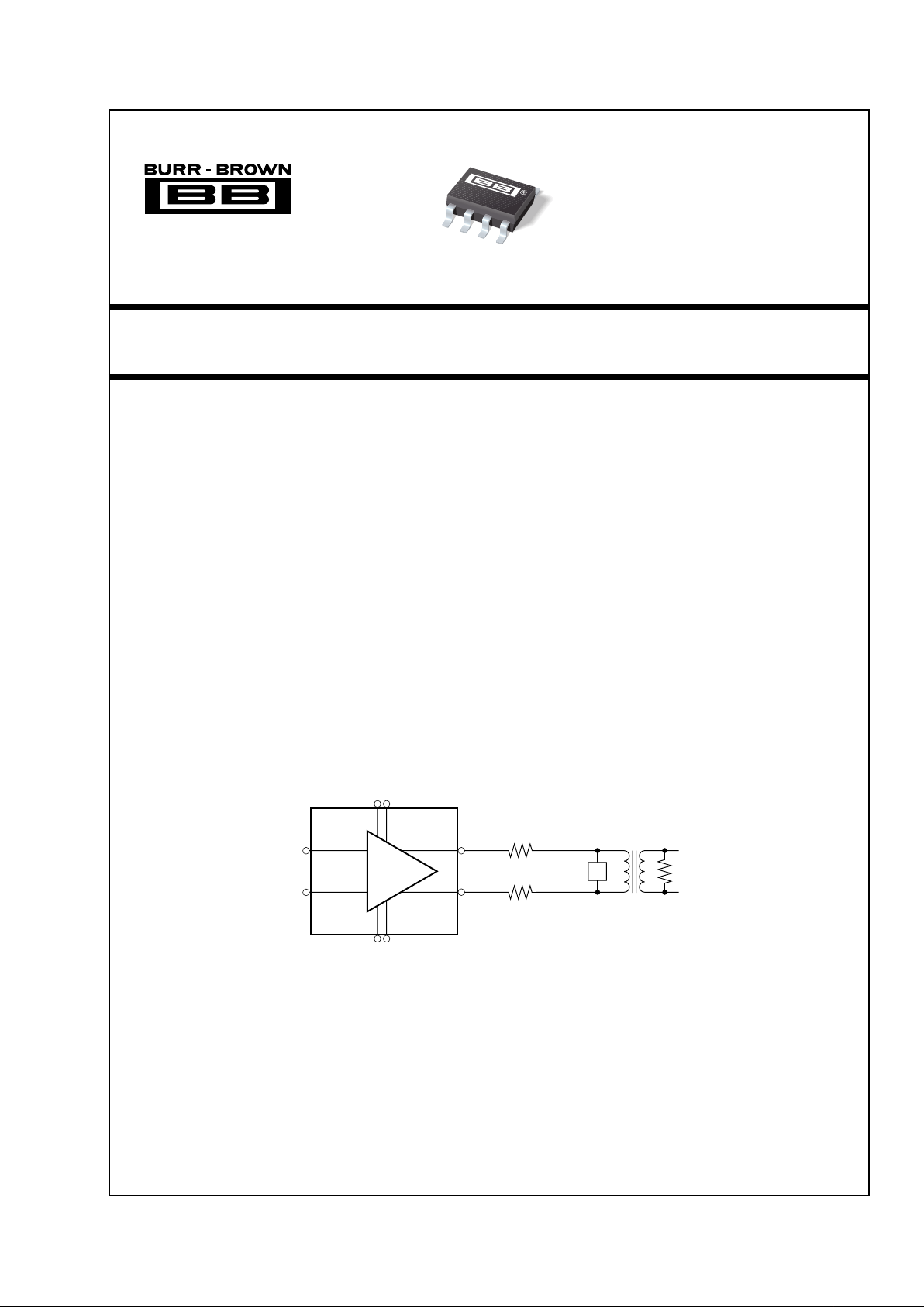
The DRV1101 is fixed gain differential line driver
designed for very low distortion operation when driving DSL line transformers. It is designed for use as the
upstream line driver for ADSL G.Lite, and as both
upstream and downstream line drivers in CAP systems. Operating on a single 5V supply, the DRV1101
can supply up to 230mA peak output current. The
output voltage can swing up to 9.5Vp-p on a single 5V
supply. In ADSL G.Lite applications, DRV1101 can
supply up to 10dBm average line power with a crest
factor of 5.3 for a peak line power delivered of
approximately 25dBm. It is packaged in a 8-lead
SOIC.
FEATURES
● HIGH OUTPUT CURRENT: 230mA
● SINGLE SUPPLY OPERATION: 5V
● 10MHz BANDWIDTH: 6Vp-p into 15Ω
● VERY LOW THD AT HIGH POWER:
–81dBc at 6Vp-p, 100kHz, 100Ω
● FIXED DIFFERENTIAL GAIN: 3V/V
APPLICATIONS
● DSL TWISTED PAIR LINE DRIVER
● COMMUNICATIONS LINE DRIVER
● TWISTED-PAIR CABLE DRIVER
©
1998 Burr-Brown Corporation PDS-1462A Printed in U.S.A. July, 1998
DRV1101
In+
In–
Out+
+5V
G = 3V/V
DRV1101
Patent
Pending
GND
Out–
4Ω
4Ω
Protection
1:3.3
Transformer
100Ω
Page 2
2
®
DRV1101
DRV1101U
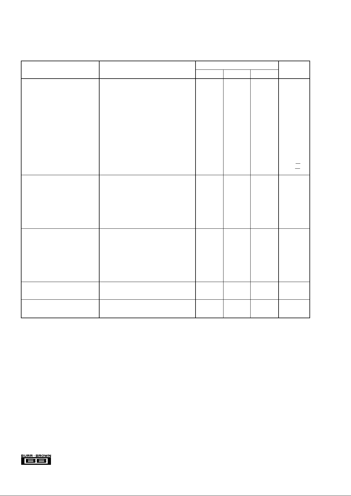
PARAMETER CONDITIONS MIN TYP MAX UNITS
AC PERFORMANCE
–3dB Bandwidth R
L
= 15Ω, VO = 1Vp-p 24 MHz
R
L
= 100Ω, VO = 1Vp-p 42 MHz
R
L
= 15Ω, VO = 6Vp-p 17 MHz
R
L
= 100Ω, VO = 6Vp-p 23 MHz
Slew Rate R
L
= 100Ω, VO = 6Vp-p 100 V/µs
Step Response Delay
(2)
VO = 1Vp-p 25 ns
Settling Time to 1%, Step Input V
O
= 1Vp-p, RL = 100Ω 0.12 µs
Settling Time to 1%, Step Input V
O
= 6Vp-p, RL = 100Ω 0.13 µs
Settling Time to 0.1%, Step Input V
O
= 1Vp-p, RL = 100Ω 0.30 µs
Settling Time to 0.1%, Step Input V
O
= 6Vp-p, RL = 100Ω 0.32 µs
THD, Total Harmonic Distortion
f = 10kHz R
L
= 100Ω, VO = 6Vp-p –88 dB
f = 10kHz R
L
= 15Ω, VO = 6Vp-p –85 dB
f = 100kHz R
L
= 100Ω, VO = 6Vp-p –83 dB
f = 100kHz R
L
= 15Ω, VO = 6Vp-p –66 –71 dB
Input Voltage Noise f = 100kHz 30 nV/√Hz
Input Current Noise f = 100kHz 0.5 fA/√Hz
INPUT
Differential Input Resistance 10
9
Ω
Differential Input Capacitance 1pF
Common-Mode Input Resistance 10
9
Ω
Common-Mode Input Capacitance 6pF
Input Offset Voltage 3mV
Input Bias Current 1nA
Common-Mode Rejection Ratio Input Referred 46 dB
Power Supply Rejection Ratio Input Referred 55 76 dB
Input Common-Mode Voltage Range
(4)
0.5 VDD –0.5 V
OUTPUT
Differential Output Offset, RTO ±10 ±30 mV
Differential Output Offset Drift, RTO –40°C to +85°C30µV/°C
Differential Output Resistance 0.16 Ω
Peak Current (Continuous) R
L
= 15Ω 200 230 mA
Differential Output Voltage Swing
(5)
RL = 1kΩ 9.8 Vp-p
R
L
= 100Ω 8.5 9.7 Vp-p
R
L
= 15Ω 7.0 Vp-p
Gain Fixed Gain, Differential 3.1 V/V
Gain Error ±0.25 dB
POWER SUPPLY
Operating Voltage Range 4.5 5.0 5.5 V
Quiescent Current V
DD
= 5.0V 25 38 mA
TEMPERATURE RANGE –40 +85 °C
Thermal Resistance,
θ
JA
8-Pin SOIC 125 °C/W
NOTES: (1) Measurement Bandwidth = 500kHz. (2) Time from 50% point of input step to 50% point of output step. (3) For step input. (4) Output common-mode voltage
follows input common-mode voltage; therefore, if input V
CM
= VDD/2, then output VCM = VDD/2. (5) THD = 1%.
SPECIFICATIONS
Typical at 25°C, VCM = VDD/2, VDD = +5.0V, unless otherwise specified.
The information provided herein is believed to be reliable; however, BURR-BROWN assumes no responsibility for inaccuracies or omissions. BURR-BROWN
assumes no responsibility for the use of this information, and all use of such information shall be entirely at the user’s own risk. Prices and specifications are subject
to change without notice. No patent rights or licenses to any of the circuits described herein are implied or granted to any third party. BURR-BROWN does not
authorize or warrant any BURR-BROWN product for use in life support devices and/or systems.
Page 3

3
®
DRV1101
PIN CONFIGURATIONS
Top View
Analog Inputs: Current .............................................. ±100mA, Momentary
±10mA, Continuous
Voltage....................................... GND –0.3V to V
DD
+0.2V
Analog Outputs Short Circuit to Ground (+25°C) ..................... Momentary
Analog Outputs Short Circuit to V
DD
(+25°C) ........................... Momentary
V
DD
to GND .............................................................................. –0.3V to 6V
Junction Temperature ................................................................... +150°C
Storage Temperature Range .......................................... –40°C to +125°C
Lead Temperature (soldering, 3s)................................................. +260°C
Power Dissipation .............................. (See Thermal/Analysis Discussion)
ABSOLUTE MAXIMUM RATINGS
PACKAGE/ORDERING INFORMATION
PACKAGE DRAWING
PRODUCT PACKAGE NUMBER
(1)
DRV1101U SO-8 Surface Mount 182
NOTE: (1) For detailed drawing and dimension table, please see end of data
sheet, or Appendix C of Burr-Brown IC Data Book.
ELECTROSTATIC
DISCHARGE SENSITIVITY
This integrated circuit can be damaged by ESD. Burr-Brown
recommends that all integrated circuits be handled with
appropriate precautions. Failure to observe proper handling
and installation procedures can cause damage.
ESD damage can range from subtle performance degradation
to complete device failure. Precision integrated circuits may
be more susceptible to damage because very small parametric
changes could cause the device not to meet its published
specifications.
In+
2
67
41
3
5
8
In–
Out+
+5V
GND
Out–
GND
In+
In–
GND
Out–
V
DD
(+5V)
V
DD
(+5V)
Out+
1
2
3
4
8
7
6
5
Page 4

4
®
DRV1101
APPLICATIONS INFORMATION
INTERNAL BLOCK DIAGRAM
The DRV1101 is a true differential input to differential
output fixed gain amplifier. Operating on a single +5V
power supply, it provides an internally fixed differential
gain of +3V/V and a common-mode gain of +1V/V from the
input to output. Fabricated on an advanced CMOS process,
it offers very high input impedance along with a low impedance 230mA output drive. Figure 1 shows a simplified
internal block diagram.
FIGURE 1. Simplified DRV1101 Internal Block Diagram.
The DRV1101 should be operated with the inputs centered
at VDD/2. This will place the output differential voltage
centered at VDD/ 2 for maximum swing and lowest distortion. Purely differential input signals will produce a purely
differential output signal. A single ended input signal, applied to one input of the DRV1101, with the other input at
a fixed voltage, will produce both a differential and common-mode output signal. This is an acceptable mode of
operation when the DRV1101 is driving an element with
good common-mode rejection (such as a transformer).
DIFFERENTIAL OUTPUT VOLTAGE AND POWER
Applying the balanced differential output voltage of the
DRV1101 to a load between the outputs will produce a peakto-peak voltage swing that is twice the swing of each
individual output. This is illustrated in Figure 2 where the
common-mode voltage is VDD/2. For a load connected
between the outputs, the only voltage that matters is the
differential voltage between the two outputs—the commonmode voltage does not produce any load current in this case.
The peak power that the DRV1101 can deliver into a differential load is V
P
2
/RL. The peak voltage (Vp) equals 1/2 of the
peak-to-peak voltage (Vp-p). Squaring 1/2 of the Vp-p and
dividing by the load impedance will give the peak power. For
example, the specifications show that on +5V supply the
DRV1101 will deliver 6.0Vp-p into 15Ω. The peak load
power under this condition is (6.0Vp-p/2)2/15Ω = 600mW.
POWER SUPPLY
The DRV1101 is designed for operation on a single +5V
supply. For loads > 200Ω, each output will swing rail to rail.
This gives a peak-to-peak differential output swing that is
approximately = 2 • VDD. For best distortion performance,
the power supply should be decoupled to a good ground
plane immediately adjacent to the package with a 0.1µF
capacitor. In addition, a larger electrolytic supply decoupling
capacitor (6.8µF) should be near the package but can be
shared among multiple devices.
DIGITAL SUBSCRIBER LINE APPLICATIONS
The DRV1101 is designed for the high power, low distortion, requirements of a twisted pair driver in digital communications applications. These include ADSL (Asymmetrical
Digital Subscriber Lines), and RADSL (Rate adaptive ADSL).
Figure 3 shows a typical transformer coupled xDSL line
driver configuration.
The DRV1101 is recommended as the upstream driver (CPE
equipment) for ADSL G.Lite systems. These system require
an rms line power of 10dBm with a voltage crest factor of
5.3 (crest factor is the ratio of peak to rms voltage). A
voltage crest factor of 5.3 is equivalent to a power crest
factor of about 15dB. Therefore, the peak power required at
the line for G.Lite is 25dBm. Using the basic circuit shown
in Figure 3, DRV1101 will provide this power to the line
with very low distortion.
FIGURE 2. DRV1101 Single Ended and Differential Output
Waveforms.
In+
In–
Out+
Out–
Buffer
Preamp
Out+
V
DD
/2
Out–
V
DD
/2
Load
0V
V
P
V
P
V
P
V
P
Page 5

5
®
DRV1101
To calculate the amplifier requirements for a DSL application:
1. Determine the average power that must be delivered to
the line. The amplifier must deliver twice this power to
account for the power dissipated in the series impedance
matching resistors. Therefore, add 3dB to the line power.
This is the average power delivered at the output of the
amplifier. For ADSL G.Lite (as of June 1998), the average line power is 10dBm. Adding 3dB results in an
average power at the amplifier output of 13dBm.
2. Next add the power crest factor needed for the line code
used. The power crest factor for ADSL is 15dB which
means that the peak power (P
PEAK
) needed at the ampli-
fier output is 28dBm (13dBm +15dB). 28dBm is 631mW.
3. The DRV1101 peak output voltage is calculated by the
formula: V
PEAK
= (P
PEAK
• RL)
1/2
where RL is the load
impedance that the DRV1101 must drive. For ADSL
Lite, using the circuit shown in Figure 3, V
PEAK
= (P
PEAK
• RL)
1/2
= (.631W x 17Ω)
1/2
= 3.3V. The peak-to-peak
voltage out of the DRV1101 is 2 x 3.3V = 6.6V.
4. The transformer turns ratio can be changed to keep the
required output voltage and current within the range of the
DRV1101. The line impedance (R
LINE
) is 100Ω for ADSL.
The impedance that is reflected to the DRV1101 side of
the transformer is R
LINE
/(turns ratio)2. For best power
transfer, the total of the impedance matching resistors
should equal the reflected impedance. Thus, for the circuit
shown in Figure 3, the reflected impedance is 100Ω/(3.4)
2
= 8.6Ω. With two impedance matching resistors of 4Ω
each and about 0.5Ω transformer resistance, the total load
impedance is about (8.6Ω + 4Ω + 4Ω + 0.5Ω) = 17Ω.
FIGURE 3. Typical Digital Subscriber Line Application.
OUTPUT PROTECTION
Figure 3 also shows overvoltage and short circuit protection
elements that are commonly included in DSL applications.
Overvoltage suppressors include diodes or MOV’s. The
outputs of the DRV1101 can be momentarily shorted to
ground or to the supply without damage. The outputs are not,
however, designed for a continuous short to ground or the
supply.
POWER DISSIPATION AND THERMAL ANALYSIS
The total internal power dissipation of the DRV1101 is the
sum of a fixed overhead power that is independent of the
load plus the power dissipated internally to deliver the
average load power. The total internal power dissipation
determines the internal temperature rise when in operation.
For DSL applications with high crest factors, such as ADSL,
the average load power delivered is much lower than the
peak power required. For practical purposes, this means that
internal temperature rise is not an issue for the DRV1101 in
high-crest factor DSL applications.
With a +5V supply, the DRV1101’s typical fixed overhead
current of 22mA (out of total no-load supply current of
29mA) creates a fixed overhead power dissipation of 110mW.
The load dependent power dissipation of the DRV1101
when delivering an output voltage Vrms to a load RL is:
P = (VDD – Vrms) • (Vrms/RL)
The internal power dissipation will reach a maximum when
Vrms is equal to VDD/2. For a sinusoidal output, this
corresponds to an output Vp-p = 1.41 • VDD.
As an example, compute the power and junction temperature
under a worst case condition with
V
DD
= +5V and Vrms = 2.5V
into a 20Ω differential load. The total internal power dissipation
would be:
(110mW) + (5V – 2.5V) • (2.5V/20Ω) = 423mW
In+
In–
Out+
+5V
DRV1101
GND
Out–
4Ω
4Ω
Protection Circuits
Impedance Matching
Resistors
1:3.3
Transformer
Line Impedance
100Ω
Fixed Load Related
Page 6

6
®
DRV1101
FIGURE 5. AC-Coupled Differential Input Interface.
FIGURE 4. Junction Temperature Rise From Ambient for
the DRV1101U.
To compute the internal junction temperature, this power is
multiplied by the junction to ambient thermal impedance (to
get the temperature rise above ambient) then added to the
ambient temperature. Using the specified maximum ambient
temperature of +85°C, the junction temperature for the
DRV1101 in an SO-8 package under these worst case
conditions will be:
TJ = 85°C + 0.423W • 125°C/W = 138°C
The internal junction temperature should, in all cases, be
limited to < 150°C. For a maximum ambient temperature of
+85°C, this limits the internal temperature rise to less than
65°C. Figure 4 shows the temperature rise from ambient to
junction for loads of 15Ω and 100Ω.
INPUT INTERFACE CIRCUITS
DRV1101 is designed for operation with a differential input
centered at VDD/2. Signals that do not require DC coupling
may be connected as shown in Figure 5 through blocking
caps to a midpoint reference developed through resistor
dividers from the supply voltage. The 1MΩ bias resistors
determine four performance requirements.
• They bias the inputs at the supply midpoint.
• They provide a DC bias current path for the input of the
DRV1101.
• They set the AC input impedance of the circuit to approximately 1MΩ.
• They set the low cutoff frequency along with CB.
The bias resistors maybe set to a lower level if a lower input
impedance is desired.
R
L
1MΩ
C
B
C
B
V
1
V
2
1MΩ
100kΩ
5V
100kΩ
0.01µF
90
80
70
60
50
40
30
20
10
0
0 0.5 1 1.5
INTERNAL TEMPERATURE RISE
OF DRV1101
Temperature Rise
Load Voltage (rms)
2 2.5 3 3.5
RL = 15Ω
Limit at 85°C Ambient
RL = 100Ω
 Loading...