

Page 1
International Airport Industrial Park • Mailing Address: PO Box 11400, Tucson, AZ 85734 • Street Address: 6730 S. Tucson Blvd., Tucson, AZ 85706 • Tel: (520) 746-1111 • Twx: 910-952-1111
Internet: http://www.burr-brown.com/ • FAXLine: (800) 548-6133 (US/Canada Only) • Cable: BBRCORP • Telex: 066-6491 • FAX: (520) 889-1510 • Immediate Product Info: (800) 548-6132
©
1998 Burr-Brown Corporation PDS-1411B Printed in U.S.A. August, 1998
DRV101
®
PWM SOLENOID/VALVE DRIVER
DRV101
DRV101
FEATURES
● HIGH OUTPUT DRIVE: 2.3A
● WIDE SUPPLY RANGE: +9V to +60V
● COMPLETE FUNCTION
PWM Output
Internal 24kHz Oscillator
Digital Control Input
Adjustable Delay and Duty Cycle
Over/Under Current Indicator
● FULLY PROTECTED
Thermal Shutdown with Indicator
Internal Current Limit
● PACKAGES: 7-Lead TO-220 and 7-Lead
Surface-Mount DDPAK
APPLICATIONS
● ELECTROMECHANICAL DRIVER:
Solenoids Positioners
Actuators
High Power Relays/Contactors
Valves Clutch/Brake
● FLUID AND GAS FLOW SYSTEMS
● INDUSTRIAL CONTROL
● FACTORY AUTOMATION
● PART HANDLERS
● PHOTOGRAPHIC PROCESSING
● ELECTRICAL HEATERS
● MOTOR SPEED CONTROL
● SOLENOID/COIL PROTECTORS
● MEDICAL ANALYZERS
DESCRIPTION
The DRV101 is a low-side power switch employing a
pulse-width modulated (PWM) output. Its rugged design is optimized for driving electromechanical devices such as valves, solenoids, relays, actuators, and
positioners. The DRV101 is also ideal for driving
thermal devices such as heaters and lamps. PWM
operation conserves power and reduces heat rise, resulting in higher reliability. In addition, adjustable
PWM allows fine control of the power delivered to the
load. Time from dc output to PWM output is externally adjustable.
The DRV101 can be set to provide a strong initial
closure, automatically switching to a “soft” hold mode
for power savings. Duty cycle can be controlled by a
resistor, analog voltage, or digital-to-analog converter
for versatility. A flag output indicates thermal shutdown and over/under current limit. A wide supply
range allows use with a variety of actuators.
The DRV101 is available in 7-lead staggered TO-220
package and a 7-lead surface-mount DDPAK plastic
power package. It is specified over the extended industrial temperature range, –40°C to +85°C.
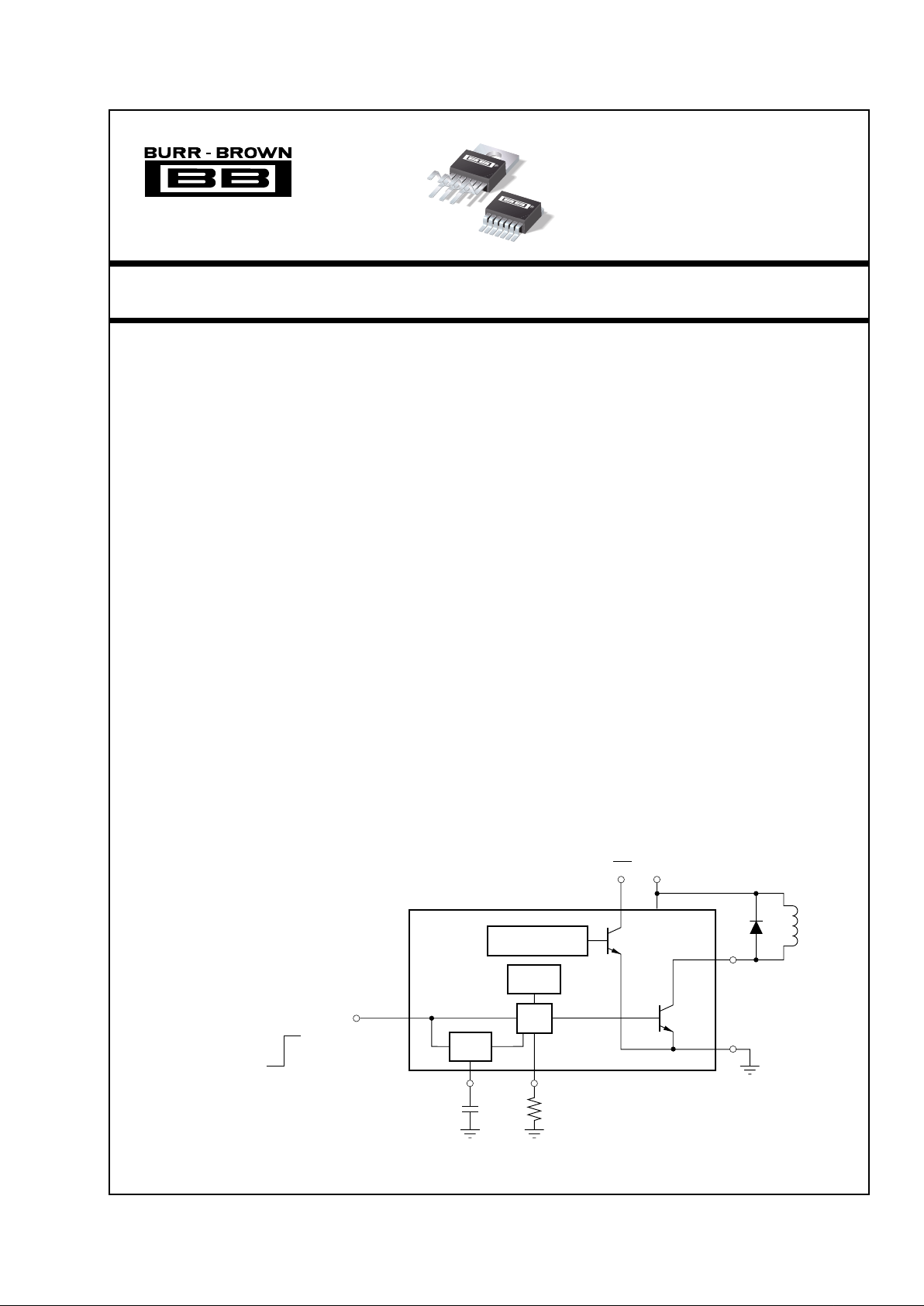
Delay
Adjust
Input
(TTL-Compatible)
On
Off
Thermal Shutdown
Over/Under Current
Flag
Load
Duty Cycle Adjust
VS (+9V to +60V)
24kHz
Oscillator
PWM
23
1
75
6
4
Gnd
Out
(electrically
connected to
tab)
Delay
Page 2
2
®
DRV101
SPECIFICATIONS
At TC = +25°C, VS = +24V, Load = 100Ω || 1000pF, and 4.99kΩ Flag pullup to +5V, unless otherwise noted.
DRV101T, F
PARAMETER COMMENTS MIN TYP MAX UNITS
OUTPUT
Output Saturation Voltage, Sink I
O
= 1A +0.8 +1 V
I
O
= 0.1A +0.2 +0.3 V
Current Limit 1.9 2.3 3 A
Under-Scale Current
(1)
23 mA
Leakage Current Output Transistor Off, V
S
= VO = +60V ±0.01 ±1mA
DIGITAL CONTROL INPUT
(2)
V
CTR
Low (output disabled) 0 +1.2 V
V
CTR
High (output enabled) +2.2 +5.5 V
I
CTR
Low (output disabled) V
CTR
= 0V –80 µA
I
CTR
High (output enabled) V
CTR
= +5V 20 µA
Propagation Delay On-to-Off and Off-to-On 2 µs
DELAY TO PWM
(3)
dc to PWM Mode
Delay Equation
(4)
Delay to PWM ≈ CD • 106 (CD in F) s
Delay Time C
D
= 0.1µF 80 95 110 ms
Minimum Delay Time
(5)
CD = 0 15 µs
DUTY CYCLE ADJUST
Duty Cycle Range 10 to 90 %
Duty Cycle Accuracy 50% Duty Cycle, R
PWM
= 28.7kΩ±2 ±5%
vs Supply Voltage 50% Duty Cycle, V
S
= VO = +9V to +60V ±1 ±5%
Nonlinearity
(6)
10% to 80% Duty Cycle 2 % FSR
DYNAMIC RESPONSE
Output Voltage Rise Time V
O
= 10% to 90% of V
S
1 2.5 µs
Output Voltage Fall Time VO = 90% to 10% of V
S
0.1 2.5 µs
Oscillator Frequency 19 24 29 kHz
FLAG
Normal Operation 20kΩ Pull-Up to +5V, I
O
< 1.5A +4 +4.9 V
Fault
(7)
Sinking 1mA +0.2 +0.8 V
Sink Current V
FLAG
= 0.4V 2 mA
Under-Current Flag: Set 4 µs
Reset 2 µs
Over-Current Flag: Set 2 µs
Reset 2 µs
THERMAL SHUTDOWN
Junction Temperature
Shutdown +165 °C
Reset from Shutdown +150 °C
POWER SUPPLY
Specified Operating Voltage +24 V
Operating Voltage Range +9 +60 V
Quiescent Current I
O
= 0 3.5 5 mA
TEMPERATURE RANGE
Specified Range –40 +85 °C
Operating Range –55 +125 °C
Storage Range –65 +150 °C
Thermal Resistance,
θ
JC
7-Lead DDPAK, 7-Lead TO-220 3 °C/W
Thermal Resistance,
θ
JA
7-Lead DDPAK, 7-Lead TO-220 No Heat Sink 65 °C/W
NOTES:(1) Under-scale current for T
C
< 100°C—see Under-Scale Current vs Temperature typical performance curve. (2) Logic High enables output (normal
operation). (3) Constant dc output to PWM (pulse-width modulated) time. (4) Maximum delay is determined by an external capacitor. Pulling the Delay Adjust Pin
low corresponds to an infinite (continuous) delay. (5) Connecting the Delay Adjust pin to +5V reduces delay time to 3µs. (6) V
IN
at pin 3 to percent of duty cycle
at pin 6. (7) A fault results from over-temperature, over-current, or under-current conditions.
The information provided herein is believed to be reliable; however, BURR-BROWN assumes no responsibility for inaccuracies or omissions. BURR-BROWN assumes
no responsibility for the use of this information, and all use of such information shall be entirely at the user’s own risk. Prices and specifications are subject to change
without notice. No patent rights or licenses to any of the circuits described herein are implied or granted to any third party. BURR-BROWN does not authorize or warrant
any BURR-BROWN product for use in life support devices and/or systems.
Page 3
3
®
DRV101
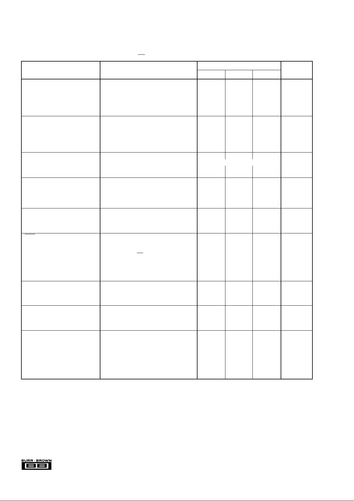
CONNECTION DIAGRAMS
Top Front View TO-220, DDPAK
Supply Voltage, V
S
.............................................................................. 60V
Input Voltage .......................................................................... –0.2V to V
S
PWM Adjust Input .................................................................. –0.2V to V
S
Delay Adjust Input ................................................ –0.2V to VS (24V max)
Operating Temperature Range ...................................... –40°C to +125°C
Storage Temperature Range ......................................... –65°C to +150°C
Junction Temperature .................................................................... +150°C
Lead Temperature (soldering, 10s)
(2)
........................................... +300°C
NOTES: (1) Stresses above these ratings may cause permanent damage.
Exposure to absolute maximum conditions for extended periods may degrade device reliability. (2) Vapor-phase or IR reflow techniques are recommended for soldering the DRV101F surface-mount package. Wave soldering
is not recommended due to excessive thermal shock and “shadowing” of
nearby devices.
ABSOLUTE MAXIMUM RATINGS
(1)
ELECTROSTATIC
DISCHARGE SENSITIVITY
This integrated circuit can be damaged by ESD. Burr-Brown
recommends that all integrated circuits be handled with
appropriate precautions. Failure to observe proper handling and
installation procedures can cause damage.
ESD damage can range from subtle performance degradation to
complete device failure. Precision integrated circuits may be more
susceptible to damage because very small parametric changes
could cause the device not to meet its published specifications.
7-Lead
Stagger-Formed
TO-220
NOTE: Tabs are electrically connected to ground (pin 4).
1234
5
6 7
7-Lead
DDPAK
Surface-Mount
PWM
PWM
Gnd Out
V
S
Delay
In
1234
5
6
Flag
Gnd Out
V
S
Delay
In
Flag
7
PACKAGE SPECIFIED
DRAWING TEMPERATURE PACKAGE ORDERING TRANSPORT
PRODUCT PACKAGE NUMBER
(1)
RANGE MARKING NUMBER
(2)
MEDIA
DRV101T 7-Lead Stagger-Formed TO-220 327 –40°C to +85°C DRV101T DRV101T Rails
DRV101F 7-Lead DDPak Surface Mount 328 –40°C to +85°C DRV101F DRV101F Rails
" " " " " DRV101F/500 Tape and Reel
NOTES: (1) For detailed drawing and dimension table, please see end of data sheet, or Appendix C of Burr-Brown IC Data Book. (2) Models with a slash (/ )
are available only in Tape and Reel in the quantities indicated (e.g., /500 indicates 500 devices per reel). Ordering 500 pieces of “DRV101F/500” will get a single
500-piece Tape and Reel. For detailed Tape and Reel mechanical information, refer to Appendix B of Burr-Brown IC Data Book.
PACKAGE/ORDERING INFORMATION
Page 4
4
®
DRV101
PIN # NAME DESCRIPTION
Pin 1 Input The input is compatible with standard TTL levels. The device output becomes enabled when the input voltage is driven above
the typical switching threshold, 1.7V. Below this level, the output is disabled. With no connection to the pin, the input level rises
to 3.4V. Input current is 20µA when driven high and 80µA with the input low. The input may be momentarily driven to the power
supply (V
S
) without damage.
Pin 2 Delay Adjust This pin sets the duration of the initial 100% duty cycle before the output goes into PWM mode. Leaving this pin floating results
in a delay of approximately 15µs, which is internally limited by parasitic capacitance. Minimum delay may be reduced to less
than 3µs by tying the pin to 5V. This pin connects internally to a 3µA current source from V
S
and to a 3V threshold comparator.
When the pin voltage is below 3V, the output device is 100% on. The PWM oscillator is not synchronized to the Input (pin 1),
so the first pulse may be extended by any portion of the programmed duty cycle.
Pin 3 Duty Cycle Adjust Internally, this pin connects to the input of a comparator and a 19kΩ resistor to ground. It is driven by a 200µA current source
(PWM) from V
S
. The voltage at this node linearly sets the duty cycle. Duty cycle can be programmed with a resistor, analog voltage,
or output of a D/A converter. The active voltage range is from 0.75V to 3.7V to facilitate the use of single-supply control
electronics. At 0.75V (or R
PWM
= 3.5kΩ), duty cycle is near 90%. Swing to ground should be limited to no lower than 0.1V. PWM
frequency is a constant 24kHz.
Pin 4 Ground This pin is electrically connected to the package tab. It must be connected to system ground for the DRV101 to function. It
carries the 3.5mA quiescent current plus the load current when the device is on.
Pin 5 V
S
This is the power supply pin. Operating range is +9V to +60V.
Pin 6 Out The output is the collector of a power npn with the emitter connected to ground. Low power dissipation in the DRV101 is attained
by the low saturation voltage and the fast switching transitions. Fall time is less than 75ns, rise time depends on load
impedance. Base drive to the power device is limited with light loads to control turn-off delay. The response of this circuit causes
the brief dip in saturation voltage after turn on. A flyback diode is needed with inductive loads to conduct the load current during
the off cycle. The external diode should be selected for low forward voltage. The internal clamp diode provides protection but
shouuld not be used to conduct load currents greater than 0.5A.
Pin 7 Flag Normally high (active low), the Flag signals either an over-temperature, over-current, or under-current fault. The over/under-
current flags are true only when the output is on (constant dc output or the “on” portion of PWM mode). A thermal fault (thermal
shutdown) occurs when the die surface reaches approximately 165°C and latches until the die cools to 150°C. Its output
requires a pull-up resistor. It can typically sink two milliamps, sufficient to drive a low-current LED.
PIN DESCRIPTIONS
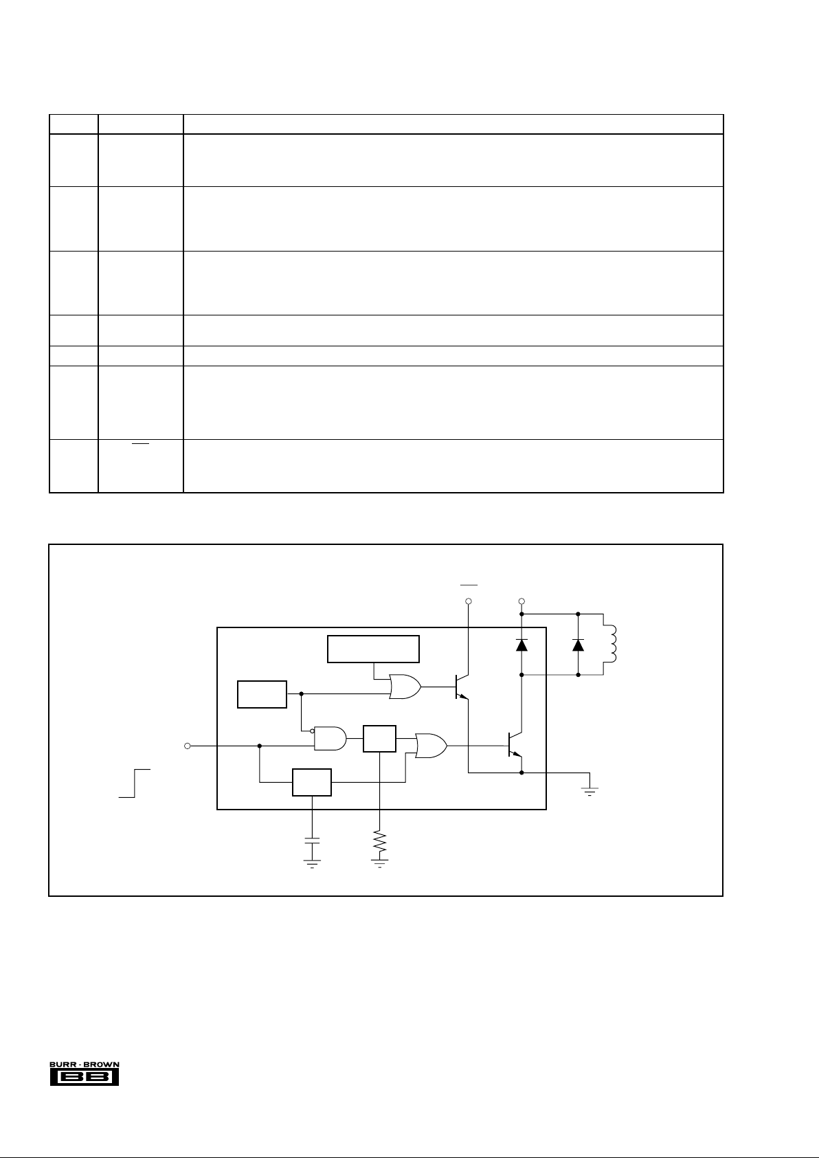
LOGIC BLOCK DIAGRAM
C
D
R
PWM
Input
On
Off
Over/Under Current
Flag
Load
VS (+9V to +60V)
Thermal
Shutdown
PWM
23
1
75
6
4
Gnd
Out
Delay
Schottky Power
Rectifier
Page 5
5
®
DRV101
DUTY CYCLE vs TEMPERATURE
–75 –50 –25 0 25 50 75 100 125
Temperature (°C)
Duty Cycle (%)
100
80
60
40
20
0
R
PWM
= 6.04kΩ
R
PWM
= 30.1kΩ
R
PWM
= 100kΩ
R
PWM
= 301kΩ
R
PWM
= 750kΩ
TYPICAL PERFORMANCE CURVES
At TC = +25°C and VS = +24V, unless otherwise noted.
CURRENT LIMIT vs TEMPERATURE
–75 –50 –25 0 25 50 75 100 125
Temperature (°C)
Current Limit (mA)
2.6
2.4
2.2
2.0
1.8
1.6
VS = +9V to +60V
QUIESCENT CURRENT vs TEMPERATURE
–75 –50 –25 0 25 50 75 100 125
Temperature (°C)
Quiescent Current (mA)
3.9
3.7
3.5
3.3
3.1
VS = +60V
VS = +9V
VS = +24V
UNDER-SCALE CURRENT vs TEMPERATURE
–75 –50 –25 0 25 50 75 100 125
Temperature (°C)
Under-Scale Current (mA)
30
25
20
15
10
5
0
VS = +9V
Lines represent maximum current
before under-current Flag occurs.
Under-current Flag may not
occur for case temperature
above 100°C.
VS = +60V
VS = +24V
DUTY CYCLE and DUTY CYCLE ERROR vs VOLTAGE
0 0.5 1.0 1.5 2.0 2.5 3.0 3.5 4.0
V
PWM
(V)
Duty Cycle (%)
Duty Cycle Error (%)
90
80
70
60
50
40
30
20
10
8
6
4
2
0
–2
–4
–6
–8
Duty Cycle
Load = 1A
Error
OUTPUT SATURATION VOLTAGE vs TEMPERATURE
–75 –50 –25 0 25 50 75 100 125
Temperature (°C)
Saturation Voltage (V)
2.5
2.0
1.5
1.0
0.5
0
IO = 2A
IO = 1A
IO = 1.5A
IO = 0.5A
IO = 0.1A
Effect of
Current-Limit
Page 6

6
®
DRV101
TYPICAL PERFORMANCE CURVES (CONT)
At TC = +25°C and VS = +24V, unless otherwise noted.
V
OUT
FLAG OPERATION
OVER-CURRENT LIMIT
(VS = +60V, CD = 110pF, R
PWM
= 750kΩ)
FLAG OPERATION
UNDER-CURRENT
(V
S
= +24V, CD = 110pF, R
PWM
= 6.04kΩ)
No Load
2A
1A
0
V
OUT
DUTY CYCLE UNDERSHOOT
Load = 1A
DC TO PWM MODE
DRIVING INDUCTIVE LOAD
(VS = +60V, CD = 110pF, R
PWM
= 301kΩ)
30V
20V
10V
0
30V
20V
10V
0
V
OUT
TYPICAL SOLENOID CURRENT WAVEFORM
(VS = +24V)
50µs/div
Inductive load ramp current
See Duty Cycle Undershoot
curve for detail
25µs/div
60V
40V
20V
0V
I
GND
1µs/div
PWM Mode
Constant Output
Flag only on during constant output
or “ON” portion of PWM mode
4V
2V
0
4V
2V
0
V
IN
V
FLAG
50µs/div
1A
0.5A
0
25ms/div
PWM Mode
OSCILLATOR FREQUENCY vs TEMPERATURE
–75 –55 –35 –15 5 25 45 65 85 105 125
Temperature (°C)
Oscillator Frequency (kHz)
24.2
24.0
23.8
23.6
23.4
VS = +9V
VS = +60V
60V
40V
20V
0
4V
2V
0
V
FLAG
Onset of
current limit
Flag only set
during constant
output mode or
“ON” portion of
PWM mode
Clean Layout
Non-optimized Layout
V
OUT
Solenoid Closure
{
Solenoid
Motion
Period
Page 7

7
®
DRV101
TYPICAL PERFORMANCE CURVES (CONT)
At TC = +25°C and VS = +24V, unless otherwise noted.
MINIMUM DELAY TO PWM vs TEMPERATURE
–75 –50 –25 0 25 50 75 100 125
Temperature (°C)
Delay (µs)
22
21
20
19
18
17
16
15
14
VS = +24V
No connection to
Delay Adjust pin
(C
D
= 0)
VS = +60V
VS = +9V
NOMINAL DELAY TIME TO PWM vs TEMPERATURE
–75 –50 –25 0 25 50 75 100 125
Temperature (°C)
Delay (ms)
104
102
100
98
96
94
92
90
88
VS = +9V
VS = +60V
VS = +24VVS = +24V
CD = 0.1µF
Page 8

8
®
DRV101
BASIC OPERATION
The DRV101 is a low-side, bipolar power switch employing
a pulse-width modulated (PWM) output for driving electromechanical and thermal devices. Its design is optimized for
two types of applications; a two-state driver (open/close) for
loads such as solenoids and actuators, and a linear driver for
valves, positioners, heaters, and lamps. Its wide supply
range, adjustable delay to PWM mode, and adjustable duty
cycle make it suitable for a wide range of applications.
Figure 1 shows the basic circuit connections to operate the
DRV101. A 0.1µF bypass capacitor is shown connected to
the power supply pin.
The Input (pin 1) is compatible with standard TTL levels.
Input voltages between +2.2V and +5.5V turn the device
output on, while pulling the pin low (0V to +1.2V), shuts the
DRV101 output off. Input current is typically 80µA.
Delay Adjust (pin 2) and Duty Cycle Adjust (pin 3) allow
external adjustment of the PWM output signal. The Delay
Adjust pin can be left floating for minimum delay to PWM
mode (typically 15µs) or a capacitor can be used to set the
delay time. Duty cycle of the PWM output can be controlled
FIGURE 1. Basic Circuit Connections and Timing Diagram.
by a resistor, analog voltage, or D/A converter. Figure 1b
provides an example timing diagram with the Delay Adjust
pin connected to 0.1µF and duty cycle set for 25%. See the
“Delay Adjust” and “Duty Cycle Adjust” text for equations
and further explanation.
Ground (pin 4) is electrically connected to the package tab.
This pin must be connected to system ground for the
DRV101 to function. This serves as the load current path to
ground, as well as the DRV101 reference ground.
The load (solenoid, valve, etc.) is connected between the
supply (pin 5) and output (pin 6). For an inductive load, an
external diode across the output is required as shown in
Figure 1a. The diode serves to maintain the hold force during
PWM operation. For remotely located loads, the external
diode should be placed close to the DRV101 (Figure 1a). The
internal clamp diode between the output and ground should
not be used to carry load current.
The Flag (pin 7) provides fault status for under-current,
over-current, and thermal shutdown conditions. This pin is
active low with pin voltage typically +0.3V during a fault
condition. A small value capacitor may be needed between
Flag and ground for noisy applications.
R
PWM
C
D
Delay
Adjust
Input
(TTL-Compatible)
On
Off
Thermal Shutdown
Over/Under Current
Flag
Load
Duty Cycle Adjust
V
S
24kHz
Oscillator
PWM
23
1
75
6
4
Gnd
Out
(electrically
connected to
tab)
Delay
0.1µF
(a)
(b)
t
P
t
ON
OUTPUT
V
S
0
INPUT
+2.2V to +5.5V
0V to +1.2V
Duty Cycle = = 25%
t
ON
t
P
R
PWM
= 130kΩ
t
ON
≈ 10.4µs
t
P
≈ 41.6µs (1/24kHz)
Basic Circuit Connections
Simplified Timing Diagram
CD = 0.1µF (95ms constant dc output before PWM)
R
PWM
= 130kΩ
(1)
NOTE: (1) External flyback diode required for inductive loads to conduct load current during the off cycle.
For remotely located loads, diode should be placed close to the DRV101.
Motorola MSRS1100T3 (1A, 100V), MBRS360T3 (3A, 60V)
CD = 0.1µF
95ms
• • •
• • •
Initial dc Output
(set by value
of C
D
)
PWM Mode
(resistor or voltage
controlled)
Page 9

9
®
DRV101
APPLICATIONS INFORMATION
POWER SUPPLY
The DRV101 operates from a single +9V to +60V supply
with excellent performance. Most behavior remains unchanged throughout the full operating voltage range. Parameters which vary significantly with operating voltage are
shown in the Typical Performance Curves.
ADJUSTABLE INITIAL 100% DUTY CYCLE
A unique feature of the DRV101 is its ability to provide an
initial constant dc output (100% duty cycle) and then switch
to PWM mode to save power. This function is particularly
useful when driving solenoids which have a much higher
pull-in current requirement than hold requirement.
The duration of this constant dc output (before PWM output
begins) can be externally controlled with a capacitor connected from Delay Adjust (pin 2) to ground according to the
following equation:
Delay Time ≈ CD • 10
6
(time in seconds, CD in Farads)
Leaving the Delay Adjust pin open results in a constant
output time of approximately 15µs. The duration of this
initial output can be reduced to less than 3µs by connecting
the pin to 5V. Table I provides examples of desired “delay”
times (constant output before PWM mode) and the appropriate capacitor values or pin connection.
CONSTANT OUTPUT DURATION C
D
3µs Pin connected to 5V
15µs Pin open
100µs 100pF
1ms 1nF
100ms 0.1µF
TABLE I. Delay Adjust Pin Connections.
ADJUSTABLE DUTY CYCLE
The DRV101’s externally adjustable duty cycle provides an
accurate means of controlling power delivered to the load.
Duty cycle can be set from 10% to 100% with an external
resistor, analog voltage, or the output of a D/A converter.
Reduced duty cycle results in reduced power dissipation.
This keeps the DRV101 and load cooler, resulting in increased reliability for both devices. PWM frequency is a
constant 24kHz.
Resistor Controlled Duty Cycle
Duty cycle is easily programmed with a resistor (R
PWM
)
connected between the Duty Cycle Adjust pin and ground.
Increased resistor values correspond to decreased duty cycles.
Table II provides resistor values for typical duty cycles.
Resistor values for additional duty cycles can be obtained
from Figure 3. For reference purposes, the equation for
calculating R
PWM
is included in Figure 3.
FIGURE 3. R
PWM
vs Duty Cycle.
FIGURE 2. Simplified Circuit Model of the Delay Adjust Pin.
The internal Delay Adjust circuitry is composed of a 3µA
current source and a 3V comparator as shown in Figure 2.
Thus, when the pin voltage is less than 3V, the output device
is 100% on (dc output mode).
3µA
2
C
D
V
S
3V Reference
Comparator
Delay Adjust
DRV101
RESISTOR
(1)
VOLTAGE
(2)
DUTY CYCLE R
PWM
(kΩ)V
PWM
(V)
10 976 3.7
20 205 3.4
30 84.5 3.0
40 46.4 2.6
50 28.7 2.2
60 18.2 1.75
70 11.8 1.35
80 7.50 1.00
90 4.87 0.75
NOTES: (1) Resistor values listed are nearest 1% standard values. (2) Do not
drive pin below 0.1V. For additional values, see “Duty Cycle vs Voltage” typical
performance curve.
TABLE II. Duty Cycle Adjust. TA= +25°C, VS = +24V.
10 20 40 60 10080
Duty Cycle (%)
R
PWM
(kΩ)
1000
100
10
1
R
PWM
= [ a + b (DC) + c (DC)2 + d (DC)3 + e (DC)4]
–1
where: a = 2.4711 x 10
–6
b = –5.2095 x 10
–7
c = 4.4576 x 10
–8
d = –7.6427 x 10
–10
e = 6.8039 x 10
–12
R
PWM
= [2.4711 x 10
–6
+ (–5.2095 x 10
–7)
(50) + (4.4576 x 10⁻⁸) (50)
2
+ (–7.6427 x 10
–10
) (50)3 + (6.8039 x 10
–12
) (50)4]
–1
DC = duty cycle in %
For 50% duty cycle:
= 28.7kΩ
Page 10

10
®
DRV101
Voltage Controlled Duty Cycle
Duty cycle can also be programmed with an analog voltage,
V
PWM
. With V
PWM
≈ 0.75V, duty cycle is near 90%. Increas-
ing this voltage results in decreased duty cycles. Table II
provides V
PWM
values for typical duty cycles. See the “Duty
Cycle vs Voltage” Typical Performance Curve for additional duty cycles.
The Duty Cycle Adjust pin should not be driven below 0.1V.
If the voltage source used can go between 0.1V and ground,
a series resistor between the voltage source and the Duty
Cycle Adjust pin (Figure 4) is required to limit swing. If the
pin is driven below 0.1V, the output will be unpredictable.
FIGURE 5. Simplified Circuit Model of the Duty Cycle
Adjust Pin.
STATUS FLAG
Flag (pin 7) provides fault indication for under-current,
over-current, and thermal shutdown conditions. During a
fault condition, Flag output is driven low (pin voltage
typically drops to 0.3V). A pull-up resistor, as shown in
Figure 6, is required to interface with standard logic. A small
value capacitor may be needed between Flag and ground in
noisy applications.
Figure 6 gives an example of a non-latching fault monitoring
circuit, while Figure 7 provides a latching version. The Flag
pin can sink several milliamps, sufficent to drive external
logic circuitry or an LED (Figure 8) to indicate when a fault
has occurred. In addition, the Flag pin can be used to turn off
other DRV101’s in a system for chain fault protection.
The DRV101’s internal 24kHz oscillator sets the PWM
period. This frequency is not externally adjustable. Duty
Cycle Adjust (pin 3) is internally driven by a 200µA current
source and connects to the input of a comparator and a 19kΩ
resistor as shown in Figure 5. The DRV101’s PWM control
design is inherently monotonic. That is, a decreased voltage
(or resistor value) always produces an increased duty cycle.
200µA
3
V
S
Comparator
Duty Cycle
Adjust
DRV101
19kΩ
Resistor or
Voltage Source
(1)
NOTE: (1) Do not drive pin below 0.1V.
3.8V
0.7V
f = 24kHz
FIGURE 4. Using a Voltage to Program Duty Cycle.
DRV101
D/A
Converter
(or analog
voltage)
1kΩ
(1)
PWM
V
PWM
V
S
3
4
6
5
Out
NOTE: (1) Required if voltage source can go below 0.1V.
DRV101
Thermal Shutdown
Over/Under Current
4
6
7
Out
5kΩ
Pull-Up
+5V
Flag
TTL or HCT
FIGURE 7. Latching Fault Monitoring Circuit.
FIGURE 6. Non-Latching Fault Monitoring Circuit.
DRV101
Thermal Shutdown
Over/Under Current
4
6
7
Out
20kΩ
+5V
Flag
Q
Q
CLR
Flag
Flag
Flag Reset
J
CLK
GND K
V
S
74XX76A
(1)
NOTE: (1) Small capacitor (10pF) may be required in noisy environments.
Page 11

11
®
DRV101
An under-current fault occurs when the output current is
below the under-scale current threshold (typically 23mA).
For example, this function indicates when the load is disconnected. Again, the flag output is not latched, so an undercurrent condition during PWM mode will produce a flag
output that is modulated by the PWM waveform. An initial,
brief under-current flag normally appears driving inductive
loads and may be avoided by adding a parallel resistor
sufficient to move the initial current above the under-current
threshold. An under-current flag may not appear for case
temperatures above 100°C. Avoid adding capacitance to pin
6 (Out) as it may cause momentary current limiting.
Over-Temperature Fault
A thermal fault occurs when the die reaches approximately
165°C, producing a similar effect as pulling the input low.
Internal shutdown circuitry disables the output and resets the
Delay Adjust pin. The Flag is latched in the low state (fault
condition) until the die has cooled to approximately 150°C.
A thermal fault can occur in any mode of operation. Recovery from thermal fault will start in delay mode (constant dc
output).
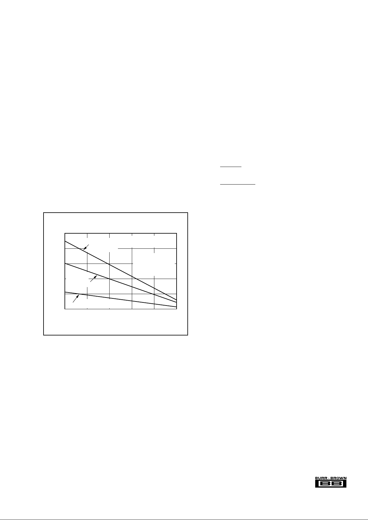
PACKAGE MOUNTING
Figure 9 provides recommended PCB layouts for both the
TO-220 and DDPAK power packages. The tab of both
packages is electrically connected to ground (pin 4). It may
be desirable to isolate the tab of TO-220 package from its
mounting surface with a mica (or other film) insulator (see
FIGURE 9. TO-220 and DDPAK Solder Footprints.
7-Lead DDPAK
(1)
(Package Drawing #328)
7-Lead TO-220
(Package Drawing #327)
NOTE: (1) For improved thermal performance increase footprint area.
See Figure 11, “Thermal Resistance vs Circuit Board Copper Area”.
Mean dimensions in inches. Refer to end of data sheet
or Appendix C of Burr-Brown Data Book for tolerances
and detailed package drawings.
0.335
0.15
0.05
0.45
0.51
0.105
0.05
0.035
0.04
0.2
0.085
Over/Under Current Fault
An over-current fault occurs when the output current is
greater than approximately 2.3A. The status flag is not
latched. Since current during PWM mode is switched on and
off, the flag output will be modulated with PWM timing (see
flag waveforms in the Typical Performance Curves).
FIGURE 8. LED to Indicate Fault Condition.
DRV101
Thermal Shutdown
Over/Under Current
4
6
7
Out
5kΩ
+5V
Flag
(LED)
HLMP-Q156
Page 12
12
®
DRV101
Figure 10). For lowest overall thermal resistance, it is best to
isolate the entire heat sink/DRV101 structure from the
mounting surface rather than to use an insulator between the
semiconductor and heat sink.
For best thermal performance, the tab of the DDPAK surface-mount version should be soldered directly to a circuit
board copper area. Increasing the copper area improves heat
dissipation. Figure 11 shows typical thermal resistance from
junction-to-ambient as a function of the copper area.
POWER DISSIPATION
Power dissipation depends on power supply, signal, and load
conditions. Power dissipation is equal to the product of
output current times the voltage across the conducting output transistor times the duty cycle. Power dissipation can be
minimized by using the lowest possible duty cycle necessary
to assure the required hold force.
Application Bulletin AB-039 explains how to calculate or
measure power dissipation with unusual signals and loads.
THERMAL PROTECTION
Power dissipated in the DRV101 will cause the junction
temperature to rise. The DRV101 has thermal shutdown
circuitry that protects the device from damage. The thermal
protection circuitry disables the output when the junction
temperature reaches approximately +165°C, allowing the
device to cool. When the junction temperature cools to
approximately +150°C, the output circuitry is again enabled.
Depending on load and signal conditions, the thermal protection circuit may cycle on and off. This limits the dissipation
of the amplifier but may have an undesirable effect on the
load.
Any tendency to activate the thermal protection circuit
indicates excessive power dissipation or an inadequate heat
sink. For reliable operation, junction temperature should be
limited to +125°C, maximum. To estimate the margin of
safety in a complete design (including heat sink), increase
the ambient temperature until the thermal protection is
triggered. Use worst-case load and signal conditions. For
good reliability, thermal protection should trigger more than
40°C above the maximum expected ambient condition of
your application. This produces a junction temperature of
125°C at the maximum expected ambient condition.
The internal protection circuitry of the DRV101 was designed to protect against overload conditions. It was not
intended to replace proper heat sinking. Continuously running the DRV101 into thermal shutdown will degrade reliability.
FIGURE 11. DDPAK Thermal Resistance vs Circuit Board Copper Area.
FIGURE 10. TO-220 Thermal Resistance vs Aluminum Plate Area.
012345678
18
16
14
12
10
8
Thermal Resistance
JA
(°C/W)
Aluminum Plate Area (inches2)
THERMAL RESISTANCE
vs ALUMINUM PLATE AREA
Aluminum Plate Area
Flat, Rectangular
Aluminum Plate
DRV101
TO-220 Package
θ
0.030in Al
0.062in Al
0.050in Al
Vertically Mounted
in Free Air
Optional mica or film insulator
for electrical isolation. Adds
approximately 1°C/W.
Aluminum
Plate Thickness
THERMAL RESISTANCE vs
CIRCUIT BOARD COPPER AREA
50
40
30
20
10
0
Thermal Resistance, θ
JA
(°C/W)
012345
Copper Area (inches
2
)
DRV101
DDPAK
Surface-Mount Package
1oz. copper
Circuit Board Copper Area
DRV101
DDPAK
Surface-Mount Package
Page 13
13
®
DRV101
Heat Sink Selection Example
A TO-220 package is dissipating 5 Watts. The maximum
expected ambient temperature is 35°C. Find the proper heat
sink to keep the junction temperature below 125°C.
Combining Equations 1 and 2 gives:
TJ = TA + PD(
θ
JC
+
θ
CH
+
θ
HA
) (3)
TJ, TA, and PD are given.
θ
JC
is provided in the specification
table, 3°C/W.
θ
CH
can be obtained from the heat sink
manufacturer. Its value depends on heat sink size, area, and
material used. Semiconductor package type, mounting screw
torque, insulating material used (if any), and thermal
joint compound used (if any) also affect
θ
CH
. A typical
θ
CH
for a TO-220 mounted package is 1°C/W. Now we can solve
for
θ
HA
:
(4)
To maintain junction temperature below 125°C, the heat
sink selected must have a
θ
HA
less than 14°C/W. In other
words, the heat sink temperature rise above ambient must be
less than 70°C (14°C/W x 5W). For example, at 5 Watts
Thermalloy model number 6030B has a heat sink
temperature rise of 66°C above ambient (
θ
HA
= 66°C/5W =
13.2°C/W), which is below the 70°C required in this example. Figure 12 shows power dissipation versus ambient
temperature for a TO-220 package with a 6030B heat sink.
Another variable to consider is natural convection versus
forced convection air flow. Forced-air cooling by a small fan
can lower
θ
CA
(
θ
CH
+
θ
HA
) dramatically. Heat sink manufacturers provide thermal data for both of these cases. For
additional information on determining heat sink requirements, consult Application Bulletin AB-038.
As mentioned earlier, once a heat sink has been selected, the
complete design should be tested under worst-case load and
signal conditions to ensure proper thermal protection.
HEAT SINKING
Most applications will not require a heat sink to assure that
the maximum operating junction temperature (125°C) is not
exceeded. However, junction temperature should be kept as
low as possible for increased reliability. Junction temperature can be determined according to the equation:
TJ = TA + P
DθJA
(1)
where,
θ
JA
=
θ
JC
+
θ
CH
+
θ
HA
(2)
TJ= Junction Temperature (°C)
TA= Ambient Temperature (°C)
PD= Power Dissipated (W)
θ
JC
= Junction-to-Case Thermal Resistance (°C/W)
θ
CH
= Case-to-Heat Sink Thermal Resistance (°C/W)
θ
HA
=
Heat Sink-to-Ambient Thermal Resistance (°C/W)
θ
JA
= Junction-to-Air Thermal Resistance (°C/W)
Figure 12 shows maximum power dissipation versus ambient temperature with and without the use of a heat sink.
Using a heat sink significantly increases the maximum
power dissipation at a given ambient temperature as shown.
FIGURE 12. Maximum Power Dissipation vs Ambient
Temperature.
The difficulty in selecting the heat sink required lies in
determining the power dissipated by the DRV101. For dc
output into a purely resistive load, power dissipation is simply
the load current times the voltage developed across the
conducting output transistor times the duty cycle. Other loads
are not as simple. Consult Application Bulletin AB-039 for
further insight on calculating power dissipation. Once power
dissipation for an application is known, the proper heat sink
can be selected.
θ
HA
=
T
J–TA
P
D
–
θ
JC
+
θ
CH
()
θ
HA
=
125°C–35°C
5W
– 3°C/W +1°C/W
()
=14°C/ W
10
8
6
4
2
0
Power Dissipation (Watts)
0 25 50 75 100 125
Ambient Temperature (°C)
MAXIMUM POWER DISSIPATION
vs AMBIENT TEMPERATURE
TO-220 with Thermalloy
6030B Heat Sink
JA
= 16.7°C/W
PD = (TJ (max) – TA) /
JA
TJ (max) = 125°C
With infinite heat sink
(
JA
= 3°C/W),
max P
D
= 33W
at T
A
= 25°C
θ
θ
DDPAK
JA
= 26°C/W
(3 in
2
one oz
copper mounting pad)
θ
DDPAK or TO-220
JA
= 65°C/W (no heat sink)
θ
θ
Page 14

14
®
DRV101
APPLICATION CIRCUITS
FIGURE 13. Fluid Flow Control System.
DRV101
Thermal Shutdown
Over/Under Current
24kHz
Oscillator
PWM
Delay
Gnd
TTL Control Input
Off
On
Flexible Tube
Plunger
Pinch Valve
Solenoid Coil
Out
6
4
57
2
1
C
DRPWM
3
V
S
(+9V to +60V)
Flag
Delay
Adjust
Duty Cycle Adjust
(1)
(10% to 100%)
Can drive most types
of solenoid-actuated
valves and actuators
NOTE: (1) Duty cycle can be programmed by
a resistor, analog voltage, or D/A converter.
Do not drive below 0.1V.
Microprocessor
+5V
5kΩ
FIGURE 14. Instrument Light Dimmer Circuit.
FIGURE 15. 4-20mA Input to PWM Output.
DRV101
Coil
Duty Cycle Adjust
Input
(On/Off)
5
V
S
6
4
1
3
4-20mA
NOTE: (1) Rectifier diode required for inductive
loads to conduct load current during the off cycle.
(1)
100Ω
187Ω
DRV101
Lamp
Cadmium Sulfide
Optical Detector
(Clairex CL70SHL
or CLSP5M)
Aimed at
ambient
light
On/Off
λ
Brighter light results in
increased duty cycle
5
6
4
10kΩ
V
S
Page 15

15
®
DRV101
FIGURE 16. Temperature Controller.
DRV101
V
S
On/Off
On/Off
Heating Element
Thermistor
Duty Cycle
Adjust
(a)
(b)
Higher temperature results in lower duty cycle
5
1
3
6
4
DRV101
REF200
V
S
V
S
Heating
Element
Duty Cycle
Adjust
5
1
32
NC
6
12
4
0.1µF
0.1µF
2µF Film
7
2
3
4
6
10µF
100µA 100µA
1kΩ
10kΩ
10MΩ
OPA134
IN4148
(1)
or
Thermistor
5kΩ at +25°C
20kΩ
4.7V
Integrator improves accuracy
NOTE: (1) Or any common silicon diode suited
to the mechanical mounting requirements.
Temperature
Control
7, 8
R
1
R
2
Page 16

16
®
DRV101
DRV101
dc Tachometer Coupled to Motor
T
+12V
5
6
4
R
1
R
2
Duty Cycle
3
Speed Control
(1)
M
NOTE: (1) Select R1/R2 ratio based on tachometer output voltage.
Input
(On/Off)
1
FIGURE 17. Constant Speed Motor Control.
FIGURE 18. DC Motor Speed Control Using AC Tachometer.
One-Shot
–15V
5nF
NP0
VFC32
0V to +10V
1kΩ
40kΩ
DRV101
2
DC
Motor
Duty Cycle
Adjust
3
5
6
4
1
100kΩ
470kΩ
Frequency In
22kΩ
47kΩ
10kΩ
M
T
AC
Tachometer
Coupled to Motor
+40V
+15V
+15V
0.5µF
1nF
2N2222
Speed Control Input
V
OUT
Delay Adjust
Open circuit will
provide 3.4V
“on” signal
Page 17

17
®
DRV101
FIGURE 19. Three-Phase Stepper Motor Driver Provides High-Stepping Torque.
DRV101
DRV101
DRV101
Phase 1
Stepper
Logic In
Phase 3
Stepper
Logic In
Phase 2
Stepper
Logic In
+V
S
M
Only one DRV101 is turned
on at sequence time
DRV101
Lamp
5
1
6
4
3
R
2
VS = +9V to +60V
R
1
R
3
4.87kΩ
R
4
4.87kΩ
C
1
20µF
+
4.3V
DIN5229
Duty Cycle Adjust
after soft start
Select R1 and R2 to divide
down V
S
to 5.5V max.
For example: with V
S
= 60V
R
1
= 11kΩ, R2 = 1kΩ
V
S
VIN = • 60V = 5V
Sets start-up
duty cycle
1kΩ
1kΩ + 11kΩ
FIGURE 20. Soft-Start Circuit for Incandescent Lamps and Other Sensitive Loads.
Page 18

18
®
DRV101
Load
5
6
4
20Ω
(10W)
DRV101
P-Channel
MOSFET
IRF4905
12V
70A
+12V
FIGURE 21. High Power, High-Side Driver.
FIGURE 22. High Power, Time Delay, Low-Side Driver.
FIGURE 23. Very High Power, Low-Side Driver.
120Ω
(2W)
750Ω
DRV101
N-Channel
IGBT
IRGPC50F
480V
27A
2N3725A
2N3725A
MPSA56
V
S
+12V
5
6
4
Load
NOTE: Duty cycle is inverted. For example, to achieve 25% duty cycle, program 75%.
Load
12V
50A
Out
5
1
6
4
32
12Ω
(20W)
1.4kΩ
1kΩ
DRV101
N-Channel
MOSFET
IRFZ48N
R
PWM
(2)
C
D
(1)
+12V
NOTES: (1) CD controls “OFF” time (turn-on delay). (2) Duty cycle is inverted.
Page 19
19
®
DRV101
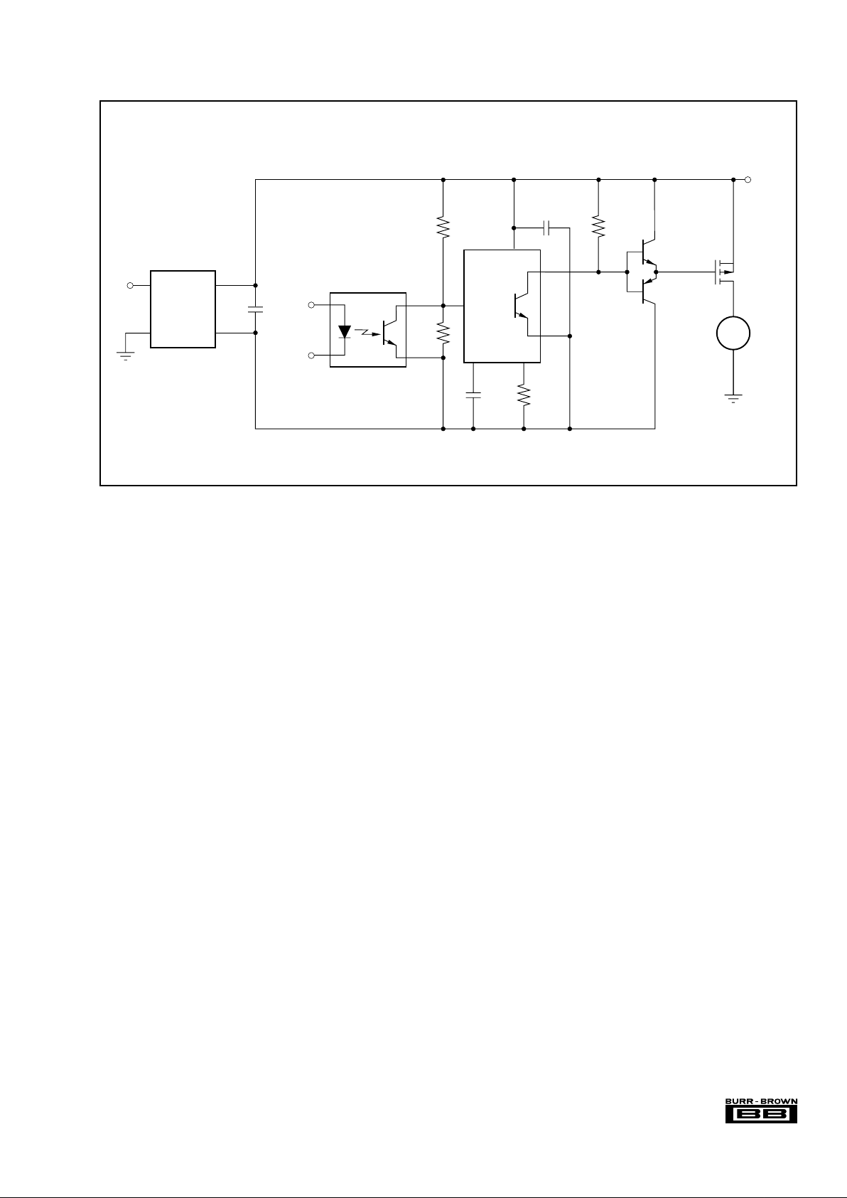
FIGURE 24. Isolated High-Side Driver.
Load
200Ω
R
PWM
C
D
2.7kΩ
2kΩ
DRV101
P-Channel
MOSFET
IRF9640
2N3725A
MPSA56
+170V
5
6
1
23
4
Control
In
0.1µF
0.1µF
12V
+5V
+
–
DCP010512
1
2
6
5
4N32
Optocoupler
 Loading...