

Page 1
DP8430V/31V/32V-33 microCMOS Programmable
256k/1M/4M Dynamic RAM Controller/Drivers
General Description
The DP8430V/31V/32V dynamic RAM controllers provide a
low cost, single chip interface between dynamic RAM and
all 8-, 16- and 32-bit systems. The DP8430V/31V/32V generate all the required access control signal timing for
DRAMs. An on-chip refresh request clock is used to automatically refresh the DRAM array. Refreshes and accesses
are arbitrated on chip. If necessary, a WAIT
put inserts wait states into system access cycles, including
burst mode accesses. RAS
RAS
precharge time after refreshes and back to back ac-
low time during refreshes and
cesses are guaranteed through the insertion of wait states.
Separate on-chip precharge counters for each RAS
can be used for memory interleaving to avoid delayed back
to back accesses because of precharge. An additional feature of the DP8432V is two access ports to simplify dual
accessing. Arbitration among these ports and refresh is
done on chip.
Ý
Control
of Pins
(PLCC) Outputs
DP8430V 68 9 256 kbit 4 Mbytes Single Access Port
DP8431V 68 10 1 Mbit 16 Mbytes Single Access Port
DP8432V 84 11 4 Mbit 64 Mbytes Dual Access Ports (A and B)
Ý
of Address
or DTACK out-
output
Features
Y
On chip high precision delay line to guarantee critical
DRAM access timing parameters
Y
microCMOS process for low power
Y
High capacitance drivers for RAS, CAS,WEand DRAM
address on chip
Y
On chip support for nibble, page and static column
DRAMs
Y
Byte enable signals on chip allow byte writing in a word
size up to 32 bits with no external logic
Y
Can use a single clock source. Up to 33 MHz operating
frequency
Y
On board Port A/Port B (DP8432V only)/refresh arbitration logic
Y
Direct interface to all major microprocessors
Y
4 RAS and 4 CAS drivers (the RAS and CAS configuration is programmable)
Largest Direct Drive Access
DRAM Memory Ports
Possible Capacity Available
July 1993
DP8430V/31V/32V-33 microCMOS Programmable
256k/1M/4M Dynamic RAM Controller/Drivers
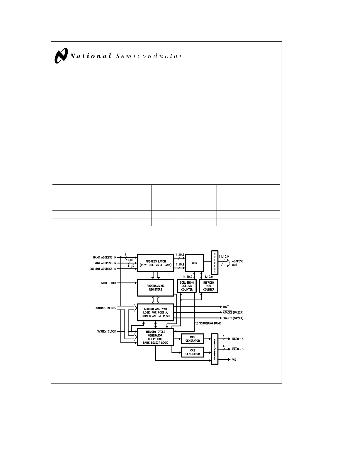
Block Diagram
DP8430V/31V/32V DRAM Controller
TRI-STATEÉis a registered trademark of National Semiconductor Corporation.
Staggered Refresh
C
1995 National Semiconductor Corporation RRD-B30M75/Printed in U. S. A.
TM
is a trademark of National Semiconductor Corporation.
TL/F/11118
FIGURE 1
TL/F/11118– 1
Page 2

Table of Contents
1.0 INTRODUCTION
2.0 SIGNAL DESCRIPTIONS
2.1 Address, R/W and Programming Signals
2.2 DRAM Control Signals
2.3 Refresh Signals
2.4 Port A Access Signals
2.5 Port B Access Signals (DP8432V)
2.6 Common Dual Port Signals (DP8432V)
2.7 Power Signals and Capacitor Input
2.8 Clock Inputs
3.0 PROGRAMMING AND RESETTING
3.1 Reset
3.2 Programming Methods
3.2.1 Mode Load Only Programming
3.2.2 Chip Selected Access Programming
3.3 Internal Programming Modes
4.0 PORT A ACCESS MODES
4.1 Access Mode 0
4.2 Access Mode 1
4.3 Extending CAS with Either Access Mode
4.4 Read-Modify-Write Cycles with Either Access Mode
4.5 Additional Access Support Features
4.5.1 Address Latches and Column Increment
4.5.2 Address Pipelining
4.5.3 Delay CAS
5.0 REFRESH OPTIONS
5.1 Refresh Control Modes
5.1.1 Automatic Internal Refresh
5.1.2 Externally Controlled Refresh
During Write Accesses
5.2 Refresh Cycle Types
5.2.1 Conventional Refresh
5.2.2 Staggered Refresh
TM
5.2.3 Error Scrubbing Refresh
5.3 Extending Refresh
6.0 PORT A WAIT STATE SUPPORT
6.1 WAIT
6.2 DTACK
Type Output
Type Output
6.3 Dynamically Increasing the Number of Wait States
6.4 Guaranteeing RAS
Low Time and RAS Precharge
Time
7.0 RAS
AND CAS CONFIGURATION MODES
7.1 Byte Writing
7.2 Memory Interleaving
7.3 Address Pipelining
7.4 Error Scrubbing
7.5 Page/Burst Mode
8.0 TEST MODE
9.0 DRAM CRITICAL TIMING PARAMETERS
9.1 Programmable Values of t
9.2 Calculation of t
RAH
and t
RAH
ASC
and t
ASC
10.0 DUAL ACCESSING (DP8432V)
10.1 Port B Access Mode
10.2 Port B Wait State Support
10.3 Common Port A and Port B Dual Port Functions
10.3.1 GRANTB Output
10.3.2 LOCK
Input
11.0 ABSOLUTE MAXIMUM RATINGS
12.0 DC ELECTRICAL CHARACTERISTICS
13.0 AC TIMING PARAMETERS
14.0 DP8430V/31V/32V USER HINTS
2
Page 3

1.0 Introduction
The DP8430V/31V/32V DRAM controllers are the latest
devices based upon the DP8420A/21A/22A predecessors.
The DP8430V/31V/32V implement changes which do not
allow them to be pin compatible with any of the DP842XA or
the DP842XV DRAM controllers. Two changes have been
made: The limits for the input frequency to DELCLK have
been increased making possible the use of a single clock
source. A RESET input is now available making the reset
procedure easier. These changes, although minimal, facilitate the use of the controllers and make them even more
attractive for high performance applications. The controllers
incorporate address latches, refresh counter, row/column/
refresh address multiplexer, delay line, refresh/access/precharge arbitration logic and high capacitive drivers. The
DP8430V/31V/32V DRAM controllers allow any manufacturer’s CPU or bus to directly interface to DRAM arrays up to
64 Mbytes in size.
Reset:
The user must reset the controller before programming it.
Reset is achieved by asserting the RESET
16 positive edges of clock.
Programming:
After reset, the user can program the controller by either
one of two methods: Mode Load Only Programming or Chip
Select Access Programming. The chip is programmed
through the address bus.
Initialization Period:
Once the DP8430V/31V/32V has been programmed for the
first time, a 60 ms initialization period is entered. During this
time the DRC performs refreshes to the DRAM array so
further warm up cycles are unnecessary. The initialization
period is entered only after the first programming after a
reset.
Accessing Modes:
After resetting and programming the chip, the DP8430V/
31V/32V is ready to access the DRAM. There are two
modes of accessing with these controllers. Mode 0, which
indicates RAS
RAS
asynchronously.
Refresh Modes:
Two refresh modes can be programmed. The user can
choose Automatic Internal Refresh or Externally Controlled
Refresh. With any refresh mode the user can perform burst
refreshes.
Refresh Types:
There are three types of refreshing available: Conventional,
Staggered and Error Scrubbing. Any refresh control mode
can be used with any type of refresh.
Wait Support:
The DP8430V/31V/32V have wait support available as
DTACK
Transfer ACKnowledge, is useful for processors whose wait
signal is active high. WAIT
whose wait signal is active low. The user can choose either
at programming. These signals are used by the on chip arbiter to insert wait states to guarantee the arbitration between
accesses, refreshes and precharge. Both signals are independent of the access mode chosen and both signals can
be dynamically delayed further through the WAITIN
the DP8430V/31V/32V.
synchronously and Mode 1, which indicates
or WAIT. Both are programmable. DTACK, Data
is useful for those processors
input for at least
signal to
Sequential Accesses (Static Column/Page Mode):
The DP8430V/31V/32V have address latches, used to
latch the bank, row and column address inputs. Once the
address is latched, a COLumn INCrement (COLINC) feature
can be used to increment the column address. The address
latches can also be programmed to be fall through. COLINC
can be used for Sequential Accesses of Static Column
DRAMs. Also, COLINC in conjunction with ECAS
be used for Sequential Accesses to Page Mode DRAMs.
RAS
and CAS Configuration (Byte Writing):
The RAS and CAS drivers can be configured to drive a one,
two or four bank memory array up to 32 bits in width. The
ECAS
signals can then be used to select one of four CAS
drivers for Byte Writing with no extra logic.
Memory Interleaving:
When configuring the DP8430V/31V/32V for more than
one bank, Memory Interleaving can be used. By tying the
low order address bits to the bank select lines B0 and B1,
sequential back to back accesses will not be delayed since
these controllers have separate precharge counters per
bank.
Address Pipelining:
The DP8430V/31V/32V are capable of performing Address
Pipelining. In address pipelining, the DRC will guarantee the
column address hold time and switch the internal multiplexor to place the row address on the address bus. At this
time, another memory access to another bank can be initiated.
Dual Accessing:
Finally, the DP8432V has all the features previously mentioned and unlike the DP8430V/31V, the DP8432V has a
second port to allow a second CPU to access the same
memory array. The DP8432V has four signals to support
Dual Accessing, these signals are AREQB
and GRANTB. All arbitration for the two ports and refresh is
done on chip by the controller through the insertion of wait
states. Since the DP8432V has only one input address bus,
the address lines must be multiplexed externally. The signal
GRANTB can be used for this purpose.
Terminology:
The following explains the terminology used in this data
sheet. The terms negated and asserted are used. Asserted
refers to a ‘‘true’’ signal. Thus, ‘‘ECAS0
the ECAS0
ed’’ means the COLINC input is at a logic 1. The term negated refers to a ‘‘false’’ signal. Thus, ‘‘ECAS0
means the ECAS0
negated’’ means the input COLINC is at a logic 0. The table
shown below clarifies this terminology.
input is at a logic 0. The term ‘‘COLINC assert-
input is at a logic 1. The term ‘‘COLINC
Signal Action Logic Level
Active High Asserted High
Active High Negated Low
Active Low Asserted Low
Active Low Negated High
inputs can
, ATACKB, LOCK
asserted’’ means
negated’’
3
Page 4
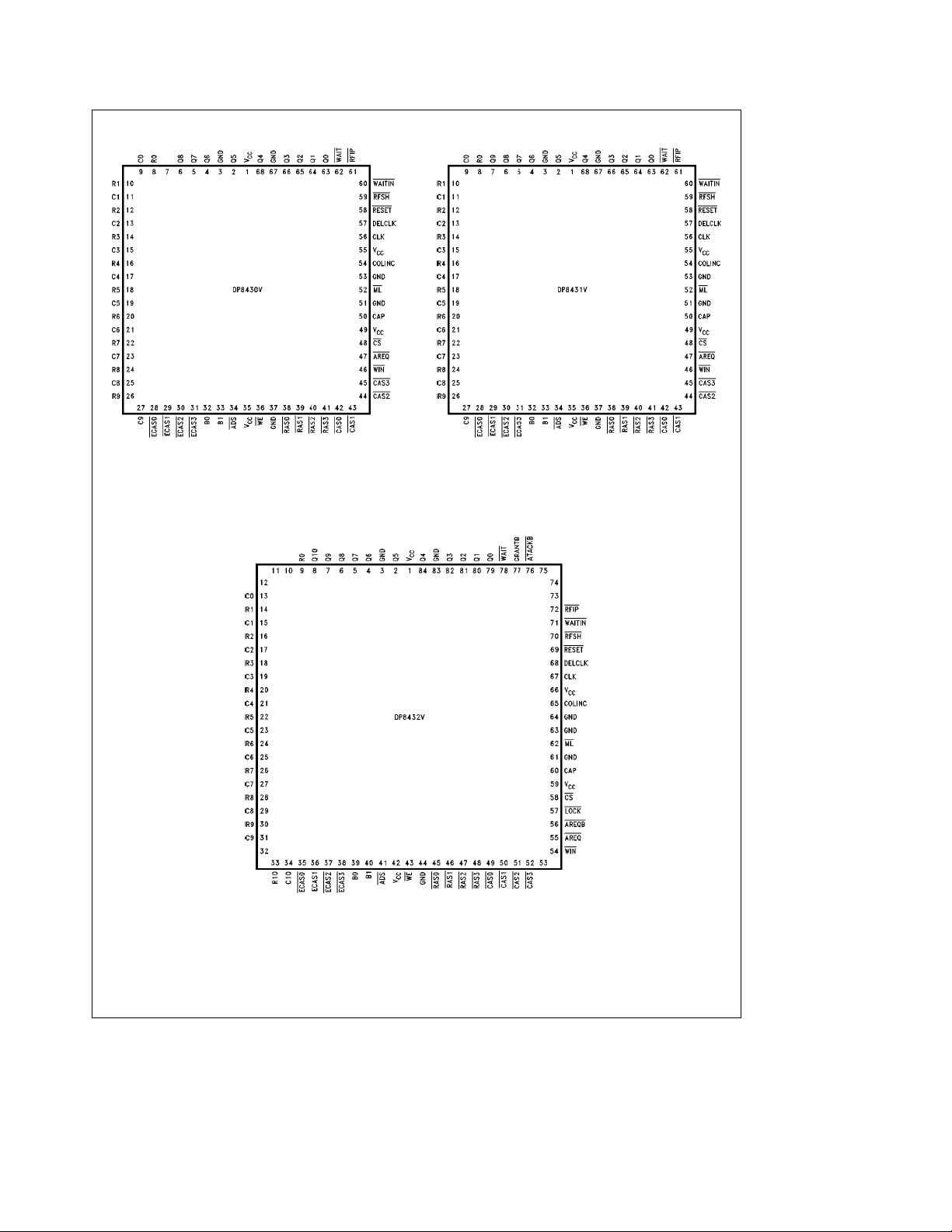
Connection Diagrams
Top View
FIGURE 2
Order Number DP8430V-33
See NS Package Number V68A
TL/F/11118– 2
Top View
FIGURE 4
Order Number DP8432V-33
See NS Package Number V84A
Top View
TL/F/11118– 3
FIGURE 3
Order Number DP8431V-33
See NS Package Number V68A
TL/F/11118– 4
4
Page 5
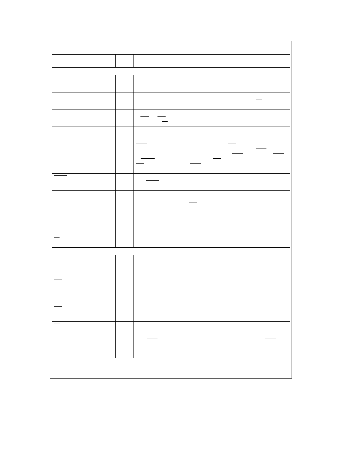
2.0 Signal Descriptions
Pin Device (If not Input/
Name Applicable to All) Output
2.1 ADDRESS, R/W AND PROGRAMMING SIGNALS
R0–10 DP8432V I ROW ADDRESS: These inputs are used to specify the row address during an access
R0–9 DP8430V/31V I
C0–10 DP8432V I COLUMN ADDRESS: These inputs are used to specify the column address during an
C0–9 DP8430V/31V I
B0, B1 I BANK SELECT: Depending on programming, these inputs are used to select a group
ECAS0–3 I ENABLE CAS: These inputs are used to enable a single or group of CAS outputs
RESET I RESET: At power up, this input is used to reset the DRAM controller. The user must
WIN I WRITE ENABLE IN: This input is used to signify a write operation to the DRAM. If
COLINC I COLUMN INCREMENT: When the address latches are used, and RFIP is negated,
(EXTNDRF) I
ML I MODE LOAD: This input signal, when low, enables the internal programming register
2.2 DRAM CONTROL SIGNALS
Q0–10 DP8432V O DRAM ADDRESS: These outputs are the multiplexed output of the R0 –9, 10 and
Q0–9 DP8431V O
Q0–8 DP8430V O
RAS0–3 O ROW ADDRESS STROBES: These outputs are asserted to latch the row address
CAS0–3 O COLUMN ADDRESS STROBES: These outputs are asserted to latch the column
WE O WRITE ENABLE or REFRESH REQUEST: This output asserted specifies a write
(RFRQ
)O
to the DRAM. They are also used to program the chip when ML
R10).
access to the DRAM. They are also used to program the chip when ML
(except C10).
of RAS and CAS outputs to assert during an access. They are also used to program
the chip when ML
when asserted. In combination with the B0, B1 and the programming bits, these
inputs select which CAS
ECAS
signals can also be used to toggle a group of CAS outputs for page/nibble
mode accesses. They also can be used for byte write operations. If ECAS
negated during programming, continuing to assert the ECAS
or AREQB during an access, will cause the CAS outputs to be extended while the
RAS
outputs are negated (the ECASn inputs have no effect during scrubbing
refreshes).
keep RESET
must remain negated (high) to avoid an unwanted reset.
ECAS0 is asserted during programming, the WE output will follow this input. This
input asserted will also cause CAS
bit C9 is asserted during programming.
this input functions as COLINC. Asserting this signal causes the column address to
be incremented by one. When RFIP
refresh cycle by any number of periods of CLK until it is negated.
that stores the programming information.
C0–9, 10 and form the DRAM address bus. These outputs contain the refresh
address whenever RFIP
series damping resistors.
contained on the outputs Q0–8, 9, 10 into the DRAM. When RFIP
RAS
outputs are used to latch the refresh row address contained on the Q0–8, 9, 10
outputs in the DRAM. These outputs contain high capacitive drivers with 20X series
damping resistors.
address contained on the outputs Q0–8, 9, 10 into the DRAM. These outputs have
high capacitive drivers with 20X series damping resistors.
operation to the DRAM. When negated, this output specifies a read operation to the
DRAM. When the DP8430V/31V/32V is programmed in address pipelining mode or
when ECAS0 is negated during programming, this output will function as RFRQ.
RFRQ
asserted, specifies that 13 msor15ms have passed. RFRQ can be used to
externally request a refresh through the input RFSH
capacitive driver and a 20X series damping resistor.
is asserted.
output or CAS outputs will assert during an access. The
low for at least 16 positive edges of clock. After programming this input
is asserted. They contain high capacitive drivers with 20X
Description
is asserted (except
is asserted
0is
0 while negating AREQ
to delay to the next positive clock edge if address
is asserted, this signal is used to extend the
is asserted, the
. This output has a high
5
Page 6
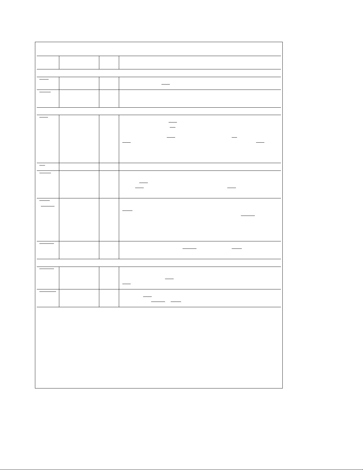
2.0 Signal Descriptions (Continued)
Pin Device (If not Input/
Name Applicable to All) Output
2.3 REFRESH SIGNALS
RFIP O REFRESH IN PROGRESS: This output is asserted prior to a refresh cycle and is
RFSH I REFRESH: This input asserted will request a refresh. If this input is continually
2.4 PORT A ACCESS SIGNALS
ADS I ADDRESS STROBE or ADDRESS LATCH ENABLE: Depending on programming,
(ALE) I
CS I CHIP SELECT: This input signal must be asserted to enable a Port A access.
AREQ I ACCESS REQUEST: This input signal in Mode 0 must be asserted some time after
WAIT O WAIT or DTACK: This output can be programmed to insert wait states into a CPU
(DTACK
)O
WAITIN I WAIT INCREASE: This input can be used to dynamically increase the number of
2.5 PORT B ACCESS SIGNALS
AREQB DP8432V I PORT B ACCESS REQUEST: This input asserted will latch the row, column and bank
ATACKB DP8432V O ADVANCED TRANSFER ACKNOWLEDGE PORT B: This output is asserted when
only
only
negated when all the RAS
asserted, the DP8430V/31V/32V will perform refresh cycles in a burst refresh
fashion until the input is negated.
this input can function as ADS
when asserted along with CS
an access will start from the positive clock edge of CLK as soon as possible. In Mode
1, the input functions as ADS
RAS
to assert if no other event is taking place. If an event is taking place, RAS will be
asserted from the positive edge of CLK as soon as possible. In both cases, the low
going edge of this signal latches the bank, row and column address if programmed to
do so.
the first positive clock edge after ALE has been asserted. When this signal is
negated, RAS
before ADS
access.
access cycle. With R7 negated during programming, the output will function as a
WAIT
With R7 asserted during programming, the output will function as DTACK
case, the output will be negated to signify a wait condition and will be asserted to
signify the access has taken place. Each of these signals can be delayed by a
number of positive clock edges or negative clock levels of CLK to increase the
microprocessor’s access cycle through the insertion of wait states.
positive clock edges of CLK until DTACK
during a DRAM access.
address if programmed, and requests an access to take place for Port B. If the
access can take place, RAS
RAS
the access RAS
the appropriate DTACK
is negated for the access. In Mode 1, this signal must be asserted
can be negated. When this signal is negated, RAS is negated for the
type output. In this case, the output will be active low to signal a wait condition.
will assert as soon as possible from a positive edge of CLK.
is asserted for a Port B access. This signal can be used to generate
or WAIT type signal for Port B’s CPU or bus.
Description
outputs are negated for that refresh.
or ALE. In mode 0, the input functions as ALE and
causes an internal latch to be set. Once this latch is set
and when asserted along with CS, causes the access
. In this
will be asserted or WAIT will be negated
will assert immediately. If the access has to be delayed,
6
Page 7
2.0 Signal Descriptions (Continued)
Pin Device (If not Input/
Name Applicable to All) Output
2.6 COMMON DUAL PORT SIGNALS
GRANTB DP8432V O GRANT B: This output indicates which port is currently granted access to the DRAM
LOCK DP8432V I LOCK: This input can be used by the currently granted port to ‘‘lock out’’ the other
2.7 POWER SIGNALS AND CAPACITOR INPUT
V
CC
GND I GROUND: Supply Voltage Reference.
CAP I CAPACITOR: This input is used by the internal PLL for stabilization. The value of the
2.8 CLOCK INPUTS
There are two clock inputs to the DP8430V/31V/32V, CLK and DELCLK. These two clocks may both be tied to the same clock
input, or they may be two separate clocks, running at different frequencies, asynchronous to each other.
CLK I SYSTEM CLOCK: This input may be in the range of 0 Hz up to 25 MHz. This input is
DELCLK I DELAY LINE CLOCK: The input frequency to DELCLK should be in the range of
only
only
array. When GRANTB is asserted, Port B has access to the array. When GRANTB is
negated, Port A has access to the DRAM array. This signal is used to multiplex the
signals R0–8, 9, 10; C0 –8, 9, 10; B0 – 1; WIN
when using dual accessing.
port from the DRAM array by inserting wait states into the locked out port’s access
cycle until LOCK is negated.
I POWER: Supply Voltage.
ceramic capacitor should be 0.1 mF and should be connected between this input and
ground.
generally a constant frequency but it may be controlled externally to change
frequencies or perhaps be stopped for some arbitrary period of time.
This input provides the clock to the internal state machine that arbitrates between
accesses and refreshes. This clock’s positive edges and negative levels are used to
extend the WAIT
RAS
precharge time and RAS low time during refresh.
All Port A and Port B accesses are assumed to be synchronous to the system clock
CLK.
12 MHz to 40 MHz. This frequency will be internally divided by choosing a divisor
when programming the part. The result of the division should be a frequency of
2 MHz. This is because the Phase Lock Loop that generates the delay line assumes
an input clock frequency of 2 MHz. If after dividing DELCLK by one of the internal
divisors (6, 8, 10, 12, 14, 16, 18 or 20) the resulting frequency is not 2 MHz, the delay
line will suffer.
For example, if the DELCLK frequency is 18 MHz and a divide by 8 is chosen,
programming bits C0–2, the resulting frequency will be 2.25 which is 12.5% off of
2 MHz. Therefore, the DP8430V/31V/32V will produce delays that are shorter (faster
delays) than what is intended. On the other hand, if divide by 10 was chosen, the
resulting frequency will be 1.8 MHz, this frequency will produce delays that are longer
(slower delays) than intended.
This clock is also divided to create the internal refresh clock.
(DTACK) signals. Ths clock is also used as the reference for the
Description
; LOCK and ECAS0–3 to the DP8432V
7
Page 8
3.0 Programming and Resetting
The DP8430V/31V/32V must be reset before it can be programmed. After reset, the DRAM controller is programmed
through the address bus by either one of two methods;
Mode Load Only Programming or Chip Select Access Programming. After the first programming after a reset, the chip
enters a 60 ms initialization period. During this period the
controller performs refreshes every 13 msor15ms, this
makes further DRAM warm up cycles unnecessary. After
this stage the DRAM controller can be programmed as
many times as the user wishes and the 60 ms initialization
period will not be entered into unless the chip is reset and
programmed again. During the 60 ms initialization period,
RFIP
is asserted and RAS toggles every 13 msor15ms
depending on the programming bit for refresh (C3). CAS
be negated and the Q outputs will count from 0 to 2047
refreshing the entire DRAM array. The initialization time period is given by the following formula. T
e
4096 * (Clock
Divisor Select) * (Refresh Clock Fine Tune)/(DELCLK Frq.)
3.1 RESET
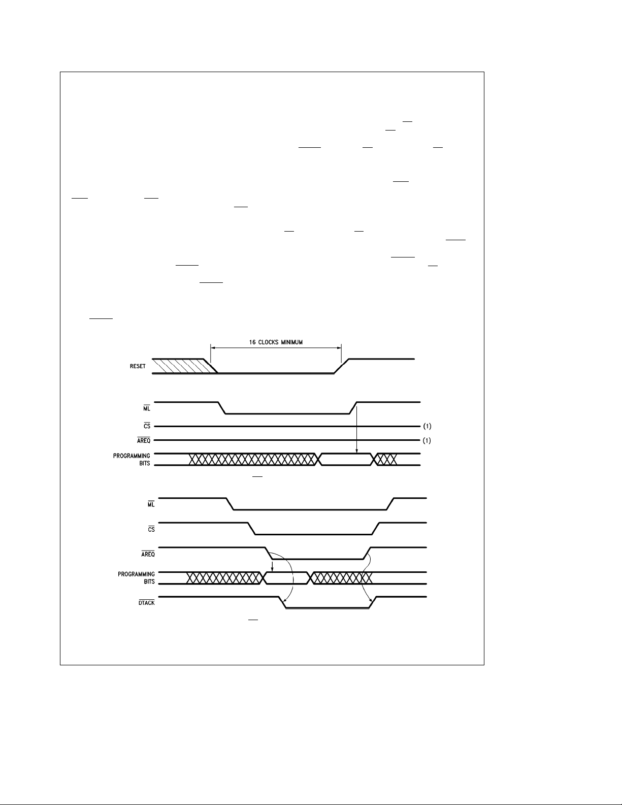
The DP8430V/31V/32V have a RESET
input pin which facilitates the reset procedure required for proper operation.
Reset is accomplished by asserting the RESET
least 16 positive edges of clock as shown in
Figure 5
The DRC may be programmed anytime on the fly, but the
user must make sure that no access or refresh is in progress. RESET
is asynchronous.
will
input for at
.
3.2 PROGRAMMING METHODS
3.2.1 Mode Load Only Programming
To use this method the user asserts ML
nal programming register. After ML
enabling the inter-
is asserted, a valid programming selection is placed on the address bus, B0, B1
and ECAS0
inputs, then ML is negated. When ML is negated the programming bits are latched into the internal programming register and the DP8430V/31V/32V is programmed, see
controller must not be refreshing, RFIP
Figure 6
. When programming the chip, the
must be high (1) to
have a successful programming.
3.2.2 Chip Selected Access Programming
The chip can also be programmed by performing a chip
selected access. To program the chip using this method,
ML
is asserted, then CS is asserted and a valid programming selection is placed on the address bus. When AREQ
asserted, the programming bits affecting the wait logic become effective immediately, then DTACK
ing the access to terminate. After the access, ML
is asserted allow-
is negated
and the rest of the programming bits take effect.
is
FIGURE 5. Reset
FIGURE 6. ML Only Programming
FIGURE 7. CS Access Programming
TL/F/11118– 5
TL/F/11118– 6
TL/F/11118– 7
8
Page 9
3.0 Programming and Resetting (Continued)
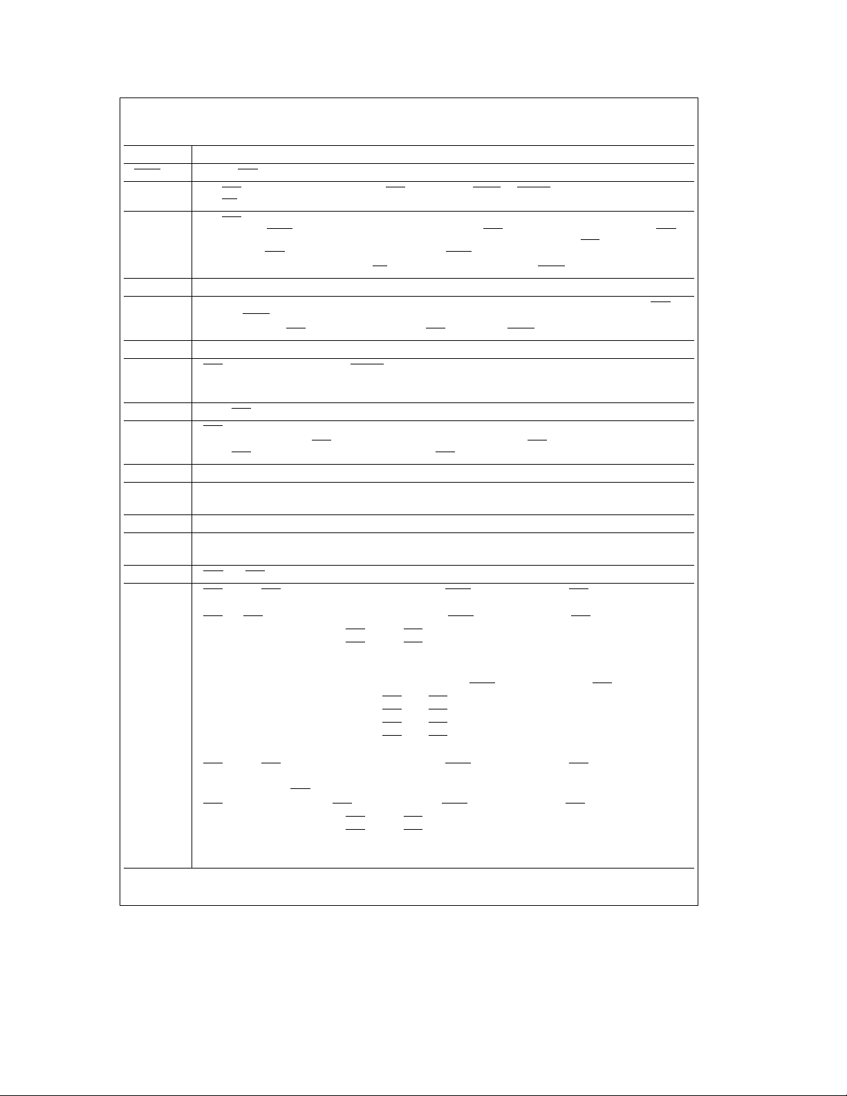
3.3 PROGRAMMING BIT DEFINITIONS
Symbol Description
ECAS0 Extend CAS/Refresh Request Select
0 The CASn outputs will be negated with the RASn outputs when AREQ (or AREQB, DP8432V only) is negated.
1 The CASn outputs will be negated, during an acccess (Port A (or Port B, DP8432V only)) when their
B1 Access Mode Select
0 ACCESS MODE 0: ALE pulsing high sets an internal latch. On the next positive edge of CLK, the access (RAS
1 ACCESS MODE 1: ADS
B0 Address Latch Mode
0 ADS or ALE asserted for Port A or AREQB asserted for Port B with the appropriate GRANT latch the input row,
1 The row, column and bank latches are fall through.
C9 Delay CAS during WRITE Accesses
0 CAS is treated the same for both READ and WRITE accesses.
1 During WRITE accesses, CAS will be asserted by the event that occurs last: CAS asserted by the internal delay
C8 Row Address Hold Time
0 Row Address Hold Timee25 ns minimum
1 Row Address Hold Timee15 ns minimum
C7 Column Address Setup Time
0 Column Address Setup Timee10 ns miniumum
1 Column Address Setup Timee0 ns minimum
C6, C5, C4 RAS and CAS Configuration Modes/Error Scrubbing during Refresh
0, 0, 0 RAS0 – 3 and CAS0–3 are all selected during an access. ECASn must be asserted for CASn to be asserted.
0, 0, 1 RAS
0, 1, 0 RAS and CAS singles are selected during an access by B0 – 1. ECAS
0, 1, 1 RAS
1, 0, 0 RAS pairs are selected by B1. CAS0 – 3 are all selected. ECASn must be asserted for CASn to be asserted.
The WE
output pin will function as write enable. Automatic Internal Refresh selected.
corresponding ECAS
outputs negating. Scrubbing refreshes are NOT affected. During scrubbing refreshes the CAS outputs will negate
along with the RAS
Externally Controlled Refresh selected, WE will function as ReFresh ReQuest (RFRQ).
will start. AREQ
column and bank address.
line or CAS
B0 and B1 are not used during an access. Error scrubbing during refresh.
and CAS pairs are selected during an access by B1. ECASn must be asserted for CAS
e
B1
0 during an access selects RAS0–1 and CAS0–1.
B1e1 during an access selects RAS2–3 and CAS2–3.
B0 is not used during an Access.
Error scrubbing during refresh.
e
B1
0, B0e0 during an access selects RAS0 and CAS0.
e
B1
0, B0e1 during an access selects RAS1 and CAS1.
e
B1
1, B0e0 during an access selects RAS2 and CAS2.
B1e1, B0e1 during an access selects RAS3 and CAS3.
Error scrubbing during refresh.
0–3 and CAS0 –3 are all selected during an access. ECASn must be asserted for CASn to be asserted.
B1, B0 are not used during an access.
No error scrubbing. (RAS
e
B1
0 during an access selects RAS0–1 and CAS0–3.
B1e1 during an access selects RAS2–3 and CAS0–3.
B0 is not used during an access.
No error scrubbing.
n inputs are negated. This feature allows the CAS outputs to be extended beyond the RAS
outputs regardless of the state of the ECAS inputs.
will terminate the access.
asserted starts the access (RAS) immediately. AREQ will terminate the access.
asserted on the positive edge of CLK after RAS is asserted.
n to be asserted.
n must be asserted for CASn to be asserted.
only refreshing)
)
9
Page 10
3.0 Programming and Resetting (Continued)
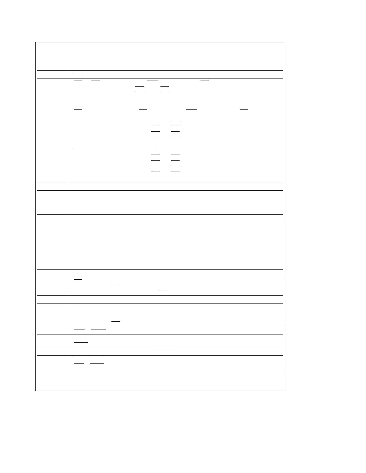
3.3 PROGRAMMING BIT DEFINITIONS (Continued)
Symbol Description
C6, C5, C4 RAS and CAS Configuration Modes (Continued)
1, 0, 1 RAS and CAS pairs are selected by B1. ECASn must be asserted for CASn to be asserted.
1, 1, 0 RAS singles are selected by B0 –1. CAS0 – 3 are all selected. ECASn must be asserted for CASntobe
1, 1, 1 RAS and CAS singles are selected by B0, 1. ECASn must be asserted for CASn to be asserted.
C3 Refresh Clock Fine Tune Divisor
0 Divide delay line/refresh clock further by 30 (If DELCLK/Refresh Clock Clock Divisore2 MHze15 ms
1 Divide delay line/refresh clock further by 26 (If DELCLK/Refresh Clock Clock Divisor
C2, C1, C0 Delay Line/Refresh Clock Divisor Select
0, 0, 0 Divide DELCLK by 20 to get as close to 2 MHz as possible.
0, 0, 1 Divide DELCLK by 18 to get as close to 2 MHz as possible.
0, 1, 0 Divide DELCLK by 16 to get as close to 2 MHz as possible.
0, 1, 1 Divide DELCLK by 14 to get as close to 2 MHz as possible.
1, 0, 0 Divide DELCLK by 12 to get as close to 2 MHz as possible.
1, 0, 1 Divide DELCLK by 10 to get as close to 2 MHz as possible.
1, 1, 0 Divide DELCLK by 8 to get as close to 2 MHz as possible.
1, 1, 1 Divide DELCLK by 6 to get as close to 2 MHz as possible.
R9 Refresh Mode Select
0 RAS0 – 3 will all assert and negate at the same time during a refresh.
1 Staggered Refresh. RAS
R8 Address Pipelining Select
0 Address pipelining is selected. The DRAM controller will switch the DRAM column address back to the row
1 Non-address pipelining is selected. The DRAM controller will hold the column address on the DRAM address
R7 WAIT or DTACK Select
0 WAIT type output is selected.
1 DTACK
R6 Add Wait States to the Current Access if WAITIN is Low
0 WAIT or DTACK will be delayed by one additional positive edge of CLK.
1 WAIT
e
B1
0 during an access selects RAS0–1 and CAS0–1.
e
B1
1 during an access selects RAS2–3 and CAS2–3.
B0 is not used during an access.
No error scrubbing.
asserted.
e
B1
0, B0e0 during an access selects RAS0 and CAS0–3.
e
B1
0, B0e1 during an access selects RAS1 and CAS0–3.
e
B1
1, B0e0 during an access selects RAS2 and CAS0–3.
e
B1
1, B0e1 during an access selects RAS3 and CAS0–3.
No error scrubbing.
e
B1
0, B0e0 during an access selects RAS0 and CAS0.
e
B1
0, B0e1 during an access selects RAS1 and CAS1.
e
B1
1, B0e0 during an access selects RAS2 and CAS2.
e
B1
1, B0e1 during an access selects RAS3 and CAS3.
No error scrubbing.
refresh period).
refresh period).
outputs during refresh are separated by one positive clock edge. Depending on the
configuration mode chosen, either one or two RAS
s will be asserted.
address after guaranteeing the column address hold time.
bus until the access RAS
s are negated.
(Data Transfer ACKnowledge) type output is selected.
or DTACK will be delayed by two additional positive edges of CLK.
e
2 MHze13 ms
10
Page 11
3.0 Programming and Resetting (Continued)
3.3 PROGRAMMING BIT DEFINITIONS (Continued)
Symbol Description
R5, R4 WAIT/DTACK during Burst (See Section 5.1.2 or 5.2.2)
0, 0 NO WAIT STATES; If R7e0 during programming, WAIT will remain negated during burst portion of access.
0, 1 1T; If R7e0 during programming, WAIT will assert when the ECAS inputs are negated with AREQ asserted.
1, 0 (/2T; If R7e0 during programming, WAIT will assert when the ECAS inputs are negated with AREQ asserted.
1, 1 0T; If R7e0 during programming, WAIT will assert when the ECAS inputs are negated. WAIT will negate when
R3, R2 WAIT/DTACK Delay Times (See Section 5.1.1 or 5.2.1)
0, 0 NO WAIT STATES; If R7e0 during programming, WAIT will remain high during non-delayed accesses. WAIT
0, 1 (/2T; If R7e0 during programming, WAIT will negate on the negative level of CLK, after the access RAS.
1, 0 NO WAIT STATES, (/2T; If R7e0 during programming, WAIT will remain high during non-delayed accesses.
1, 1 1T; If R7
R1, R0 RAS Low and RAS Precharge Time
0, 0 RAS asserted during refreshe2 positive edges of CLK.
0, 1 RAS asserted during refreshe3 positive edges of CLK.
1, 0 RAS asserted during refreshe2 positive edges of CLK.
1, 1 RAS
e
If R7
1 programming, DTACK will remain asserted during burst portion of access.
WAIT
will negate from the positive edge of CLK after the ECASs have been asserted.
If R7e1 during programming, DTACK will negate when the ECAS inputs are negated with AREQ asserted.
DTACK
will assert from the positive edge of CLK after the ECASs have been asserted.
WAIT
will negate on the negative level of CLK after the ECASs have been asserted.
e
If R7
1 during programming, DTACK will negate when the ECAS inputs are negated with AREQ asserted.
DTACK
will assert from the negative level of CLK after the ECASs have been asserted.
the ECAS
If R7e1 during programming, DTACK will negate when the ECAS inputs are negated. DTACK will assert when
the ECAS
will negate when RAS is negated during delayed accesses.
NO WAIT STATES; If R7
1T; If R7e1 during programming, DTACK will be asserted on the positive edge of CLK after the access RAS.
WAIT
(/2T; If R7
1(/2T; If R7
of CLK after the access RAS
RAS
RAS
RAS
RAS
RAS
RAS
RAS
RAS
inputs are asserted.
inputs are asserted.
e
1 during programming, DTACK will be asserted when RAS is asserted.
will negate on the negative level of CLK, after the access RAS, during delayed accesses.
e
1 during programming, DTACK will be asserted on the negative level of CLK after the access RAS.
e
0 during programming, WAIT will negate on the positive edge of CLK after the access RAS.
e
1 during programming, DTACK will be asserted on the negative level of CLK after the positive edge
precharge timee1 positive edge of CLK.
will start from the first positive edge of CLK after GRANTB transitions (DP8432V).
precharge timee2 positive edges of CLK.
will start from the second positive edge of CLK after GRANTB transitions (DP8432V).
precharge timee2 positive edges of CLK.
will start from the first positive edge of CLK after GRANTB transitions (DP8432V).
asserted during refreshe4 positive edges of CLK.
precharge timee3 positive edges of CLK.
will start from the second positive edge of CLK after GRANTB transitions (DP8432V).
.
11
Page 12

4.0 Port A Access Modes
The DP8430V/31V/32V have two general purpose access
modes. Mode 0 RAS
chronous. One of these modes is selected at programming
through the B1 input. A Port A access to DRAM is initiated
by two input signals: ADS
ways terminated by one signal: AREQ
should be synchronous to the input clock.
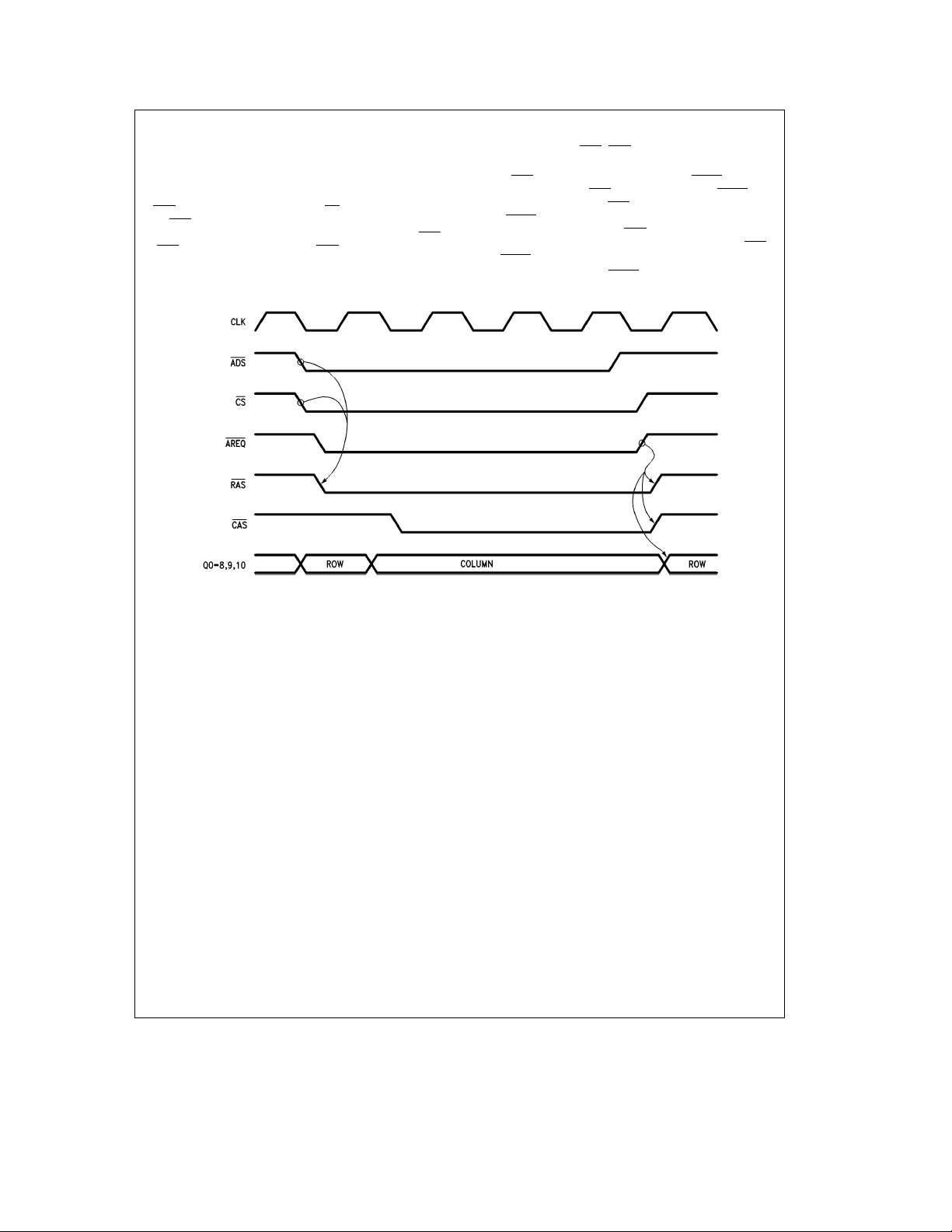
4.1 ACCESS MODE 0
Mode 0, synchronous access, is selected by negating the
input B1 during programming (B1
access, ALE is pulse high and CS
time was met, a refresh of DRAM or a Port B access was
not in progress, the RAS
synchronous and Mode 1 RAS asyn-
(ALE) and CS. The access is al-
(RASs) would be asserted on the
. These input signals
e
0). To initiate a Mode 0
is asserted. If precharge
first rising edge of clock. If a refresh or a Port B access is in
progress or precharge time is required, the controller will
wait until these events have taken place and assert RAS
(RASs) on the next positive edge of clock.
Sometime after the first positive edge of clock after ALE and
CS
have been asserted, the input AREQ must be asserted.
In single port applications, once AREQ
be negated. On the other hand, ALE can stay asserted several periods of clock; however, ALE must be negated before
or during the period of CLK in which AREQ
The controller samples AREQ on the every rising edge of
clock after DTACK
AREQ
is sampled negated.
is asserted. The access will end when
is asserted, CS can
is negated.
FIGURE 8a. Access Mode 0
12
TL/F/11118– 8
Page 13
4.0 Port A Access Modes (Continued)
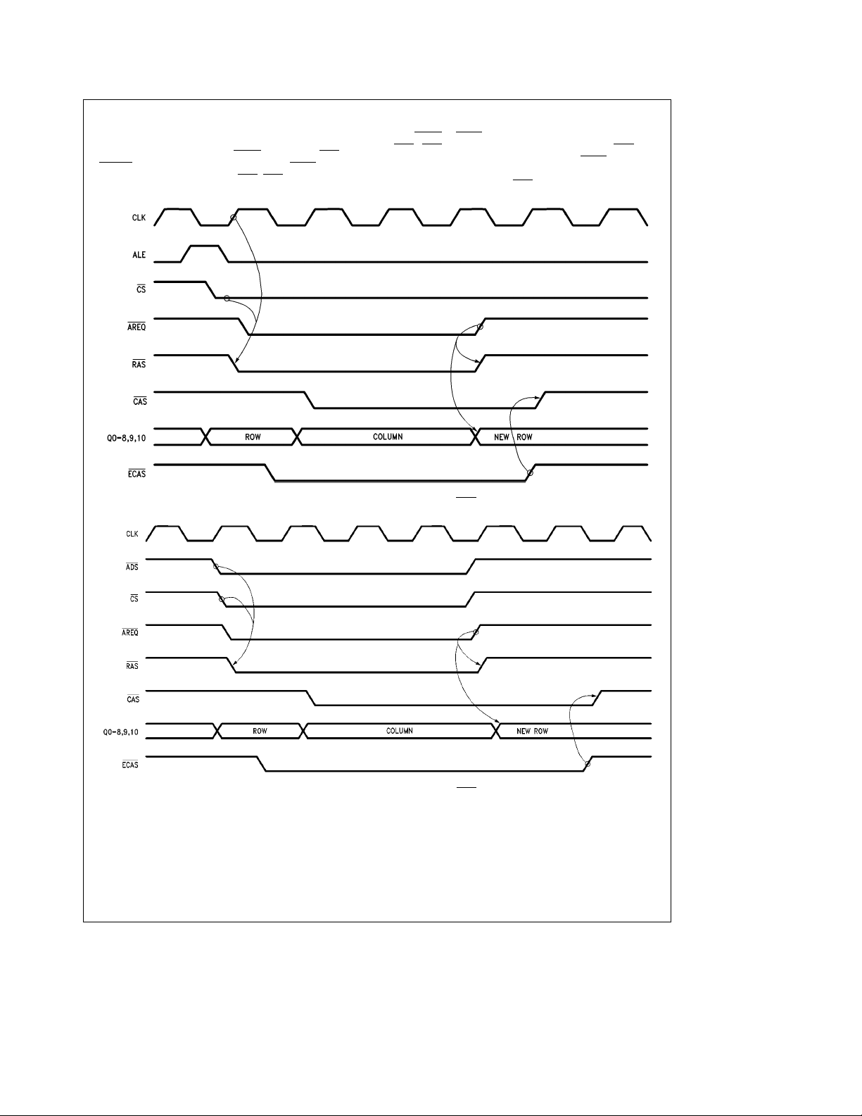
4.2 ACCESS MODE 1
Mode 1, asynchronous access, is selected by asserting the
input B1 during programming (B1
cesses to start immediately from the access request input,
ADS
. To initiate a Mode 1 access, CS is asserted followed
by ADS
asserted. If precharge time was met, a refresh of
the DRAM or a Port B access was not in progress, the RAS
(RASs) would be asserted from ADS being asserted. If a
refresh or Port B access is in progress or precharge time is
required, the controller will wait until these events have tak-
e
1). This mode allows ac-
en place and assert RAS
of clock.
When ADS
asserted. At this time, ADS
continue the access. Also, ADS
after AREQ
new access will not start until ADS
again. When address pipelining is not implemented, ADS
and AREQ can be tied together.
The access will end when AREQ is negated.
is asserted or sometime after, AREQ must be
has been asserted and negated; however, a
(RASs) from the next rising edge
can be negated and AREQ will
can continue to be asserted
is negated and asserted
FIGURE 8b. Access Mode 1
13
TL/F/11118– 9
Page 14
4.0 Port A Access Modes (Continued)
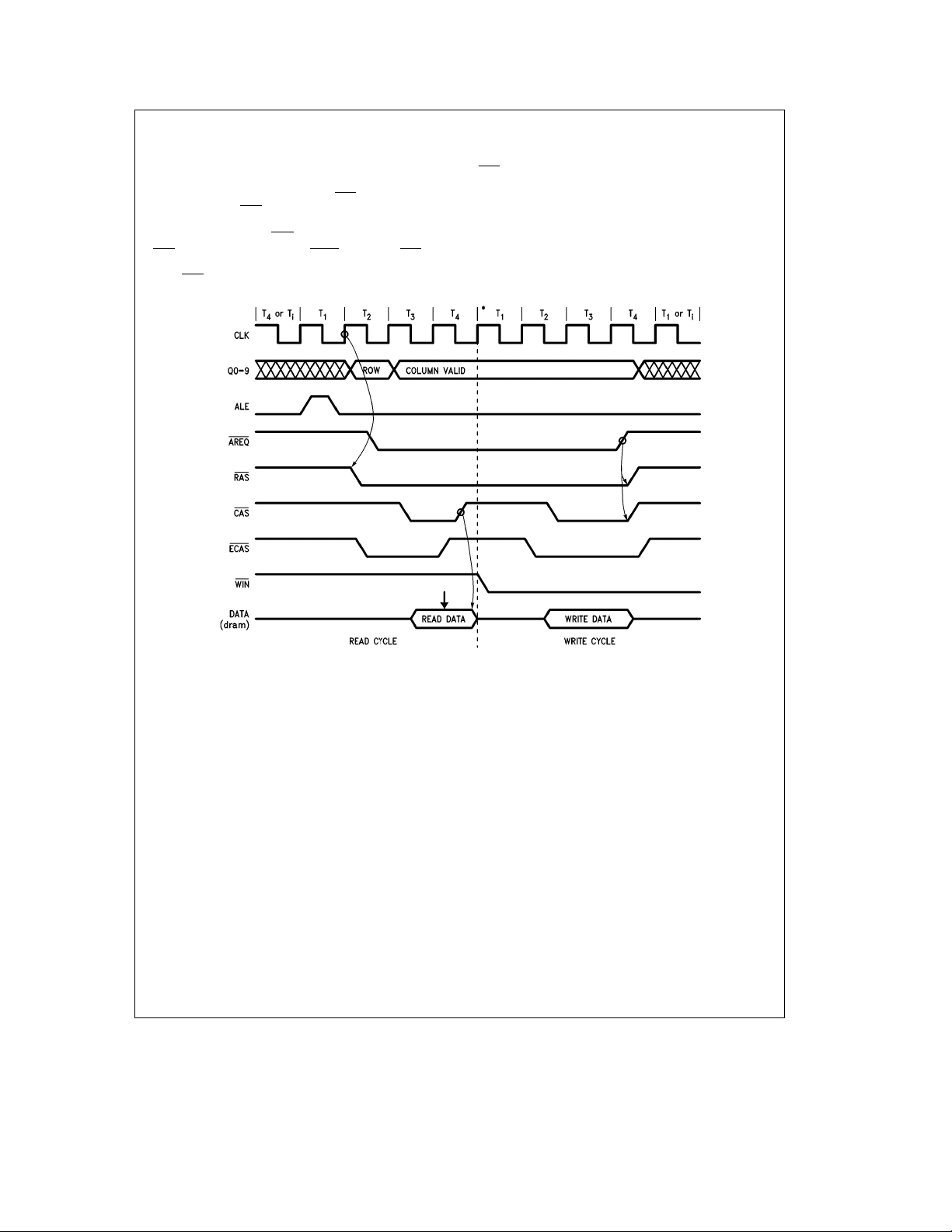
4.3 EXTENDING CAS WITH EITHER ACCESS MODE
In both access modes, once AREQ
DTACK
if programmed will be negated. If ECAS0 was as-
serted (0) during programming, CAS
is negated, RAS and
(CASs) will be negated
with AREQ
CAS
been negated, given that the appropriate ECAS
. If ECAS0 was negated (1) during programming,
(CASs) will continue to be asserted after RAS has
inputs are
asserted. This allows a DRAM to have data present on the
data out bus while gaining RAS
precharge time.
FIGURE 9a. Access Mode 0 Extending CAS
FIGURE 9b. Access Mode 1 Extending CAS
TL/F/11118– 10
TL/F/11118– 11
14
Page 15
4.0 Port A Access Modes (Continued)
4.4 READ-MODIFY-WRITE CYCLES WITH EITHER ACCESS MODE
There are 2 methods by which this chip can be used to do
read-modify-write access cycles. The first method involves
doing a late write access where the WIN
some delay after CAS
volves doing a page mode read access followed by a page
mode write access with RAS
CASn must be toggled using the ECASn inputs and WIN has
to be changed from negated to asserted (read to write)
while CAS
is negated. This method is better than changing
is asserted. The second method in-
held low (see
input is asserted
Figure 9c
).
WIN
from negated to asserted in a late write access because here a problem may arise with DATA IN and DATA
OUT being valid at the same time. This may result in a data
line trying to drive two different levels simultaneously. The
page mode method of a read-modify-write access allows
the user to have transceivers in the system because the
data in (read data) is guaranteed to be high impedance during the time the data out (write data) is valid.
*There may be idle states inserted here by the CPU.
TL/F/11118– 12
FIGURE 9c. Read-Modify-Write Access Cycle
15
Page 16
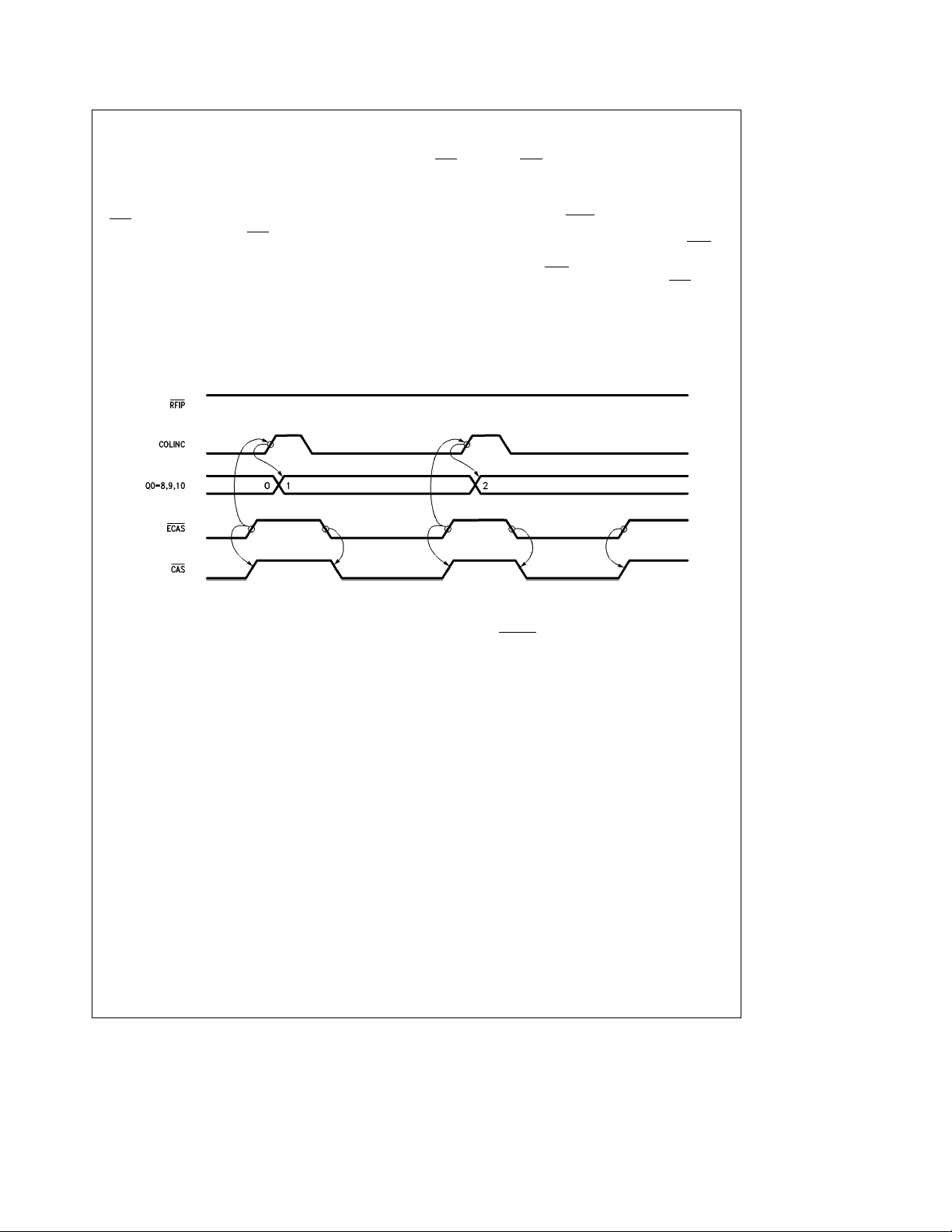
4.0 Port A Access Modes (Continued)
4.5 ADDITIONAL ACCESS SUPPORT FEATURES
To support the different modes of accessing, the DP8430V/
31V/32V offer other access features. These additional features include: Address Latches and Column Increment (for
page/burst mode support), Address Pipelining, and Delay
CAS
(to allow the user with a multiplexed bus to ensure
valid data is present before CAS
4.5.1 Address Latches and Column Increment
The Address Latches can be programmed, through programming bit B0. They can be programmed to either latch
the address or remain in a fall-through mode. If the address
latches are used to latch the address, the controller will
function as follows:
In Mode 0, the rising edge of ALE places the latches in fallthrough, once ALE is negated, the address present in the
row, column and bank input is latched.
is asserted).
In Mode 1, the address latches are in fall through mode until
ADS
is asserted. ADS asserted latches the address.
Once the address is latched, the column address can be
incremented with the input COLINC. COLINC can be used
for sequential accesses of static column DRAMs. COLINC
can also be used with the ECAS
tial accesses to page mode DRAMs as shown in
COLINC should only be asserted when the signal RFIP
negated during an access since this input functions as extended refresh when RFIP
negated (0) when the address is being latched (ADS
edge in Mode 1). If COLINC is asserted with all of the bits of
the column address asserted (ones), the column address
will return to zero.
inputs to support sequen-
Figure 10
is asserted. COLINC must be
falling
.
is
FIGURE 10. Column Increment
The address latches function differently with the DP8432V.
The DP8432V will latch the address of the currently granted
port. If Port A is currently granted, the address will be
latched as described in Section 4.5.1. If Port A is not granted, and requests an access, the address will be latched on
the first or second positive edge of CLK after GRANTB has
been negated depending on the programming bits R0, R1.
For Port B, if GRANTB is asserted, the address will be
latched with AREQB
address will latch on the first or second positive edge of
CLK after GRANTB is asserted depending on the programming bits R0, R1.
16
asserted. If GRANTB is negated, the
TL/F/11118– 13
Page 17
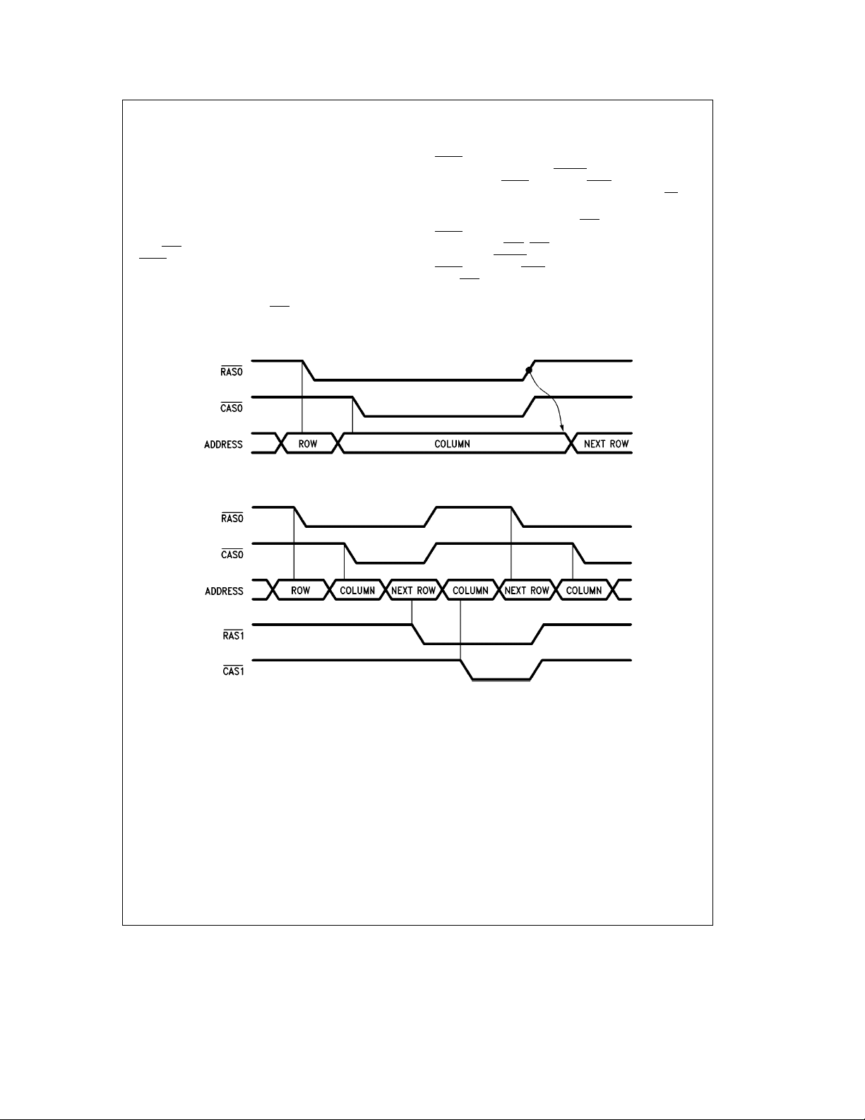
4.0 Port A Access Modes (Continued)
4.5.2 Address Pipelining
Address pipelining is the overlapping of accesses to different banks of DRAM. If the majority of successive accesses
are to a different bank, the accesses can be overlapped.
Because of this overlapping, the cycle time of the DRAM
accesses are greatly reduced. The DP8430V/31V/32V can
be programmed to allow a new row address to be placed on
the DRAM address bus after the column address hold time
has been met. At this time, a new access can be initiated
with ADS
AREQ
supports address pipelining for Port A only. This mode cannot be used with page, static column or nibble modes of
operations because the DRAM column address is switched
back to the row address after CAS
programmed through address bit R8 (see
11b
or ALE, depending on the access mode, while
is used to sustain the current access. The DP8432V
is asserted. This mode is
Figures 11a
).
and
During address pipelining in Mode 0, shown in
ALE cannot be pulsed high to start another access until
AREQ
has been asserted for the previous access for at
least one period of CLK. DTACK
negated once AREQ
insert wait states, will be asserted once ALE and CS
asserted.
In Mode 1, shown in
AREQ
is asserted. After meeting the minimum negated
pulse width for ADS
new access. DTACK
AREQ
is negated. WAIT, if programmed, will be asserted
once ADS
In either mode with either type of wait programmed, the
DP8430V/31V/32V will still delay the access for precharge
if sequential accesses are to the same bank or if a refresh
takes place.
is asserted.
is negated. WAIT, if programmed to
Figure 11d
, ADS can again be asserted to start a
, if programmed, will be negated once
, if programmed, will be
, ADS can be negated once
Figure 11c
are
,
FIGURE 11a. Non-Address Pipelined Mode
FIGURE 11b. Address Pipelined Mode
TL/F/11118– 14
TL/F/11118– 15
17
Page 18
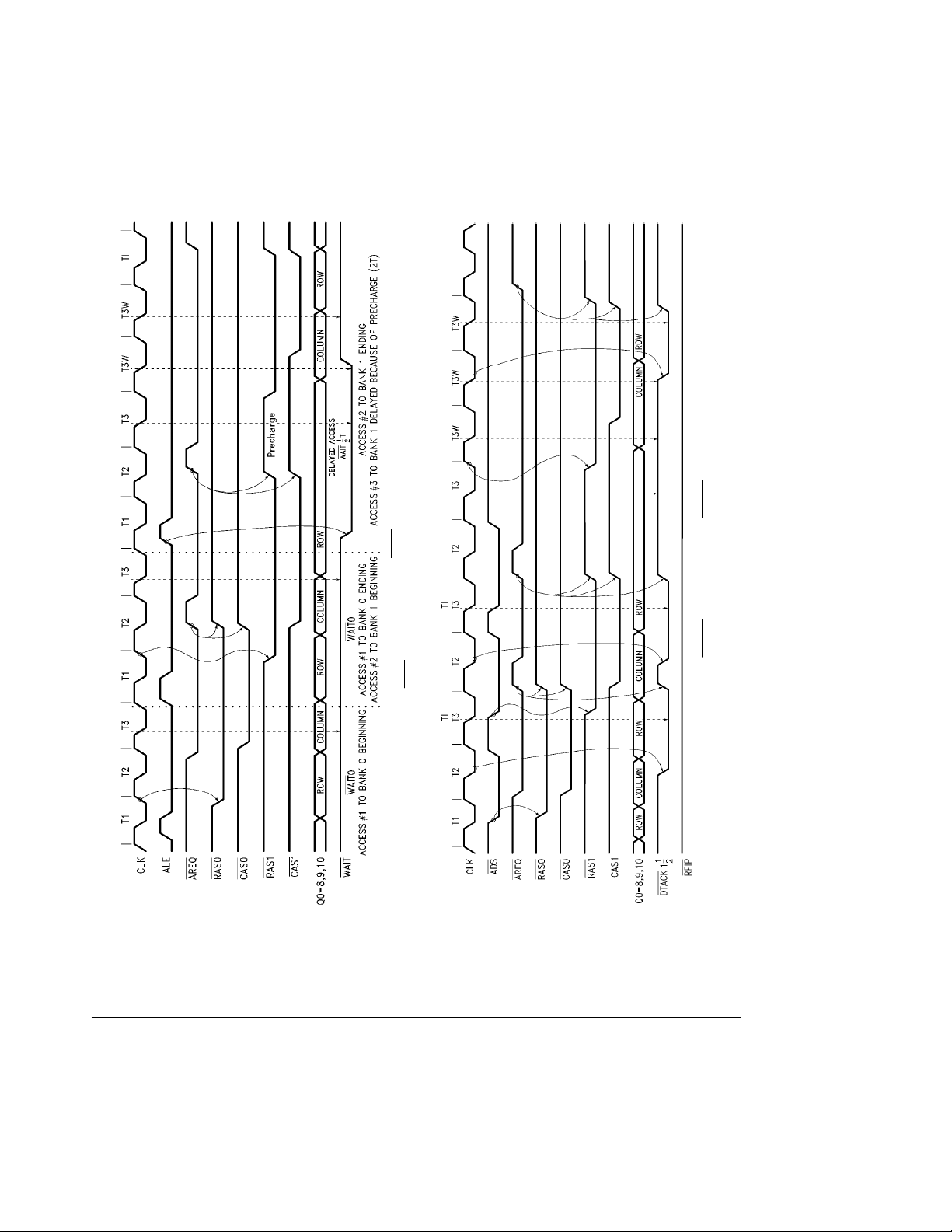
4.0 Port A Access Modes (Continued)
TL/F/11118– 16
TL/F/11118– 17
is Sampled at the ‘‘T3’’ Falling Clock Edge)
WAIT
FIGURE 11c. Mode 0 Address Pipelining (WAIT of 0, (/2T Has Been Programmed.
18
FIGURE 11d. Mode 1 Address Pipelining (DTACK 1(/2T Programmed, DTACK is Sampled at the ‘‘T3’’ Falling Clock Edge)
Page 19
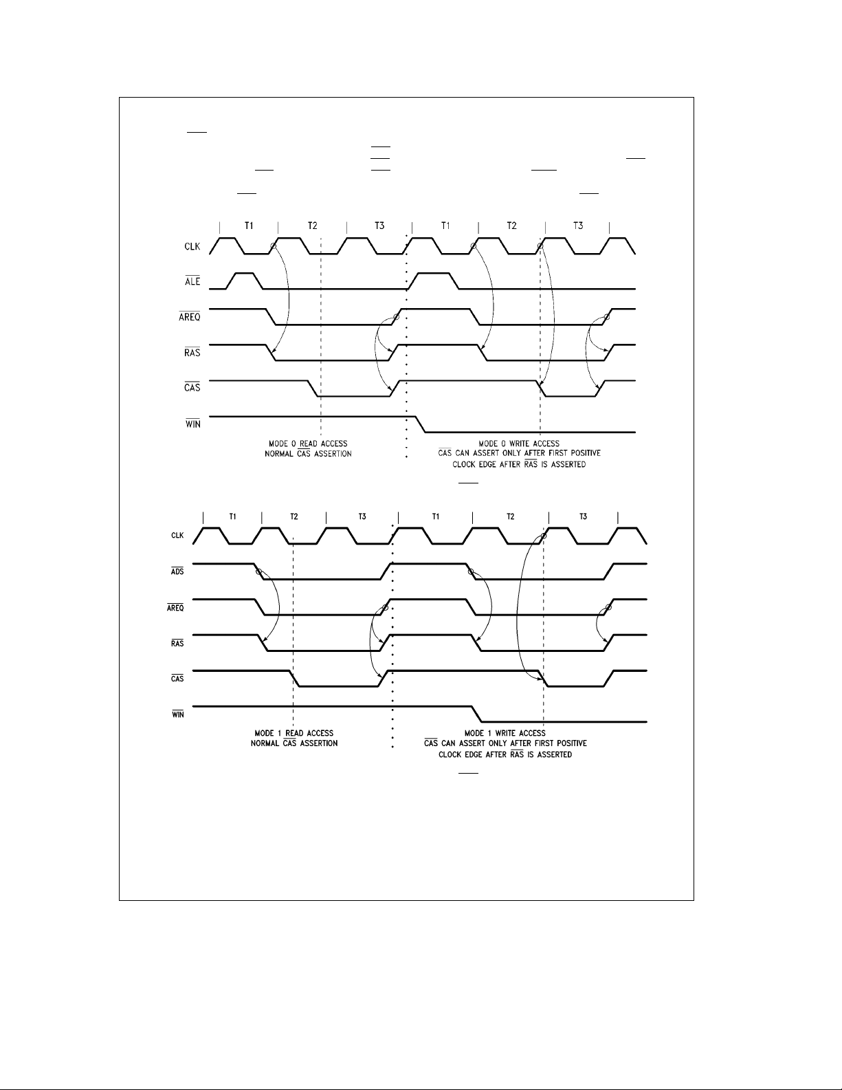
4.0 Port A Access Modes (Continued)
4.5.3 Delay CAS
Address bit C9 asserted during programming will cause CAS
to be delayed until the first positive edge of CLK after RAS
is asserted when the input WIN is asserted. Delaying CAS
during write accesses ensures that the data to be written to
DRAM will be setup to CAS
during Write Accesses
asserting as shown in
Figures
and
12b.
12a
be present after the first positive edge of CLK, CAS
delayed further with the ECAS
negated during programming, read and write accesses will
be treated the same (with regard to CAS
If the possibility exists that data still may not
can be
inputs. If address bit C9 is
).
FIGURE 12a. Mode 0 Delay CAS
FIGURE 12b. Mode 1 Delay CAS
TL/F/11118– 18
TL/F/11118– 19
19
Page 20
5.0 Refresh Options
The DP8430V/31V/32V support two refresh control mode
options:
1. Automatic Internally Controlled Refresh.
2. Externally Controlled Refresh.
With each of the control modes above, three types of refresh can be performed.
1. All RAS
2. Staggered Refresh.
3. Error Scrubbing During All RAS Refresh.
There are two inputs, EXTNDRF and RFSH
puts, RFIP
also ten programming bits: R0 – 1, R9, C0 –6 and ECAS0
used to program the various types of refreshing.
Asserting the input EXTNDRF, extends the refresh cycle for
a single or multiple integral periods of CLK.
The output RFIP
first refresh RAS
progress, RFIP
before the first refresh RAS
ted for the access (see
The DP8430V/31V/32V will increment the refresh address
counter automatically, independent of the refresh mode
used. The refresh address counter will be incremented once
all the refresh RAS
Refresh.
and two out-
and RFRQ, associated with refresh. There are
is asserted one period of CLK before the
is asserted. If an access is currently in
will be asserted up to one period of CLK
, after AREQ or AREQB is nega-
Figure 13
).
s have been negated.
In every combination of refresh control mode and refresh
type, the DP8430V/31V/32V is programmed to keep RAS
asserted a number of CLK periods. The time values of RAS
low during refresh are programmed through programming
bits R0 and R1.
5.1 REFRESH CONTROL MODES
5.1.1. Automatic Internal Refresh
To select Automatic Internal Refresh, the user must choose
e
ECAS0
0 during programming. The DP8430V/31V/32V
have an internal refresh clock. The period of the refresh
clock is generated from the programming bits C0 –3. Every
period of the refresh clock, an internal refresh request is
generated. As long as a DRAM access is not currently in
progress and precharge time has been met, the internal refresh request will generate an automatic internal refresh. If a
DRAM access is in progress, the DP8430V/31V/32V onchip arbitration logic will wait until the access is finished
before performing the refresh. The refresh/access arbitration logic can insert a refresh cycle between two address
pipelined accesses. However, the refresh arbitration logic
can not interrupt an access cycle to perform a refresh.
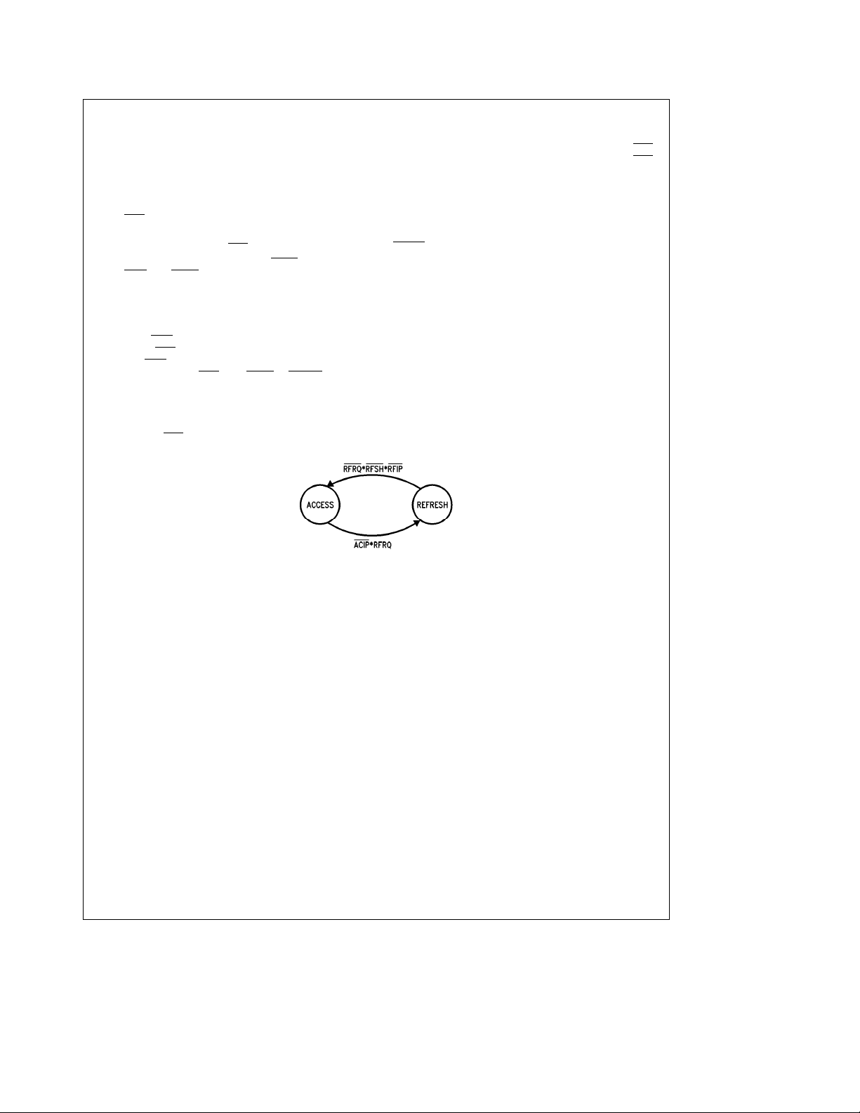
Explanation of Terms
RFRQeReFresh ReQuest internal to the DP8430V/31V/32V. RFRQ has the ability to hold off a pending access.
e
RFSH
Externally requested ReFreSH
e
RFIP
ReFresh in Progress
e
ACIP
Port A or Port B (DP8432V only) ACcess in Progress. This means that either RAS is low for an access or is in the process of
transitioning low for an access.
TL/F/11118– 20
FIGURE 13. DP8430V/31V/32V Access/Refresh Arbitration State Program
20
Page 21
5.0 Refresh Options (Continued)
5.1.2 Externally Controlled Refresh Mode
To choose this refresh mode, the user must program
e
ECAS0
sponsible for generating refresh requests by asserting the
input RFSH
this refresh mode, the output WE
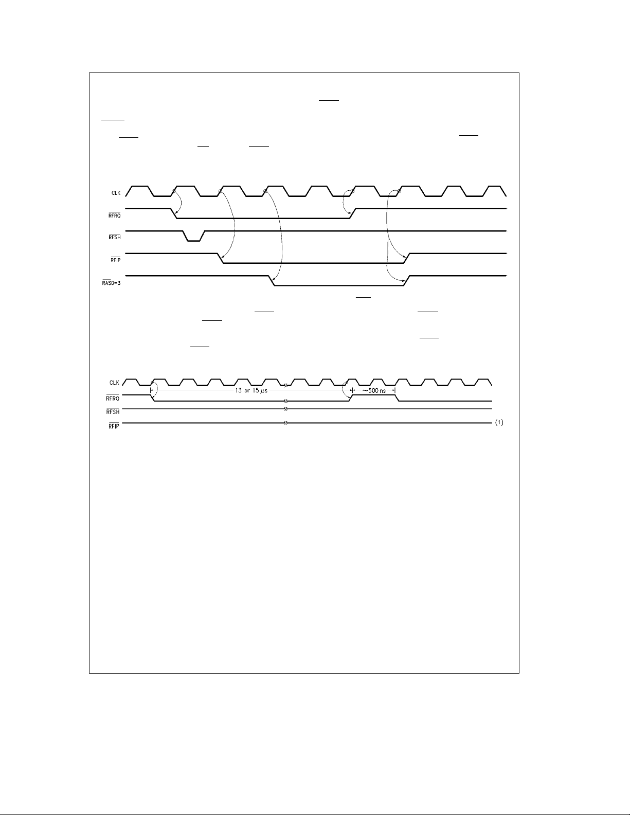
When Externally Controlled Refresh is selected, the user
may choose to monitor the output ReFresh ReQuest
1. When this mode is selected, the user is re-
every time a refresh cycle is to be performed. In
functions a RFRQ.
(RFRQ
) for an indication from the DRAM controller that a
refresh is needed. When this output asserts, it indicates that
the internal refresh clock has expired and that another refresh is necessary. Then the user has two options. First, he
can answer immediately asserting the input RFSH
ing a refresh cycle. In this case a refresh will take place
immediately if no access is in progress and precharge time
for the previous access has been met. See
request-
Figure 14a
.
FIGURE 14a. Automatic Internal Refresh with Refresh Request (3T of RAS Low during Refresh Programmed)
Second, the user may choose not to assert the RFSH
delaying the refresh until later. RFRQ
assert (toggle) if additional periods of the internal refresh
clock have expired and the user has not performed a refresh by asserting the input RFSH
critical event, or a long access like page or static column
will go high and then
. See
Figure 14b
FIGURE 14b. Refresh Request Timing
input
. If a time
mode can not be interrupted, RFRQ
used to increment an external counter. This counter can
later be used to perform a burst refresh of the number of
refreshes missed (through the RFSH
can be thought of as Refresh Request/Acknowledge.
pulsing high can be
input). This scheme
TL/F/11118– 21
TL/F/11118– 22
21
Page 22
5.0 Refresh Options (Continued)
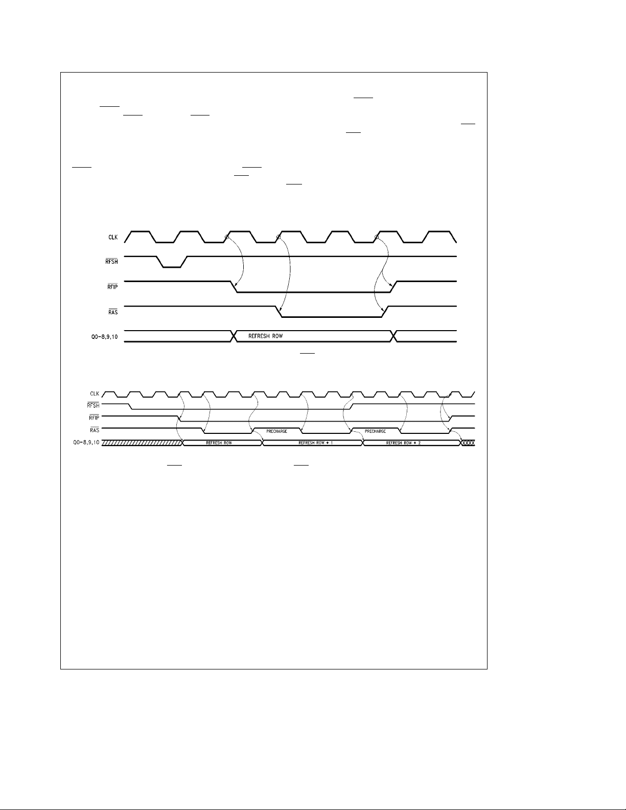
In Externally Controlled Refresh the user does not have to
wait for RFRQ
time assert the RFSH
ternal latch that is used to produce the internal refresh request. The refresh cycle will take place on the next positive
edge of clock, as shown in
DRAM is in progress or precharge time for the last access
has not been met, the refresh will be delayed. Since pulsing
RFSH
low until the refresh starts. When the last refresh RAS negates, the internal refresh request latch is cleared.
to perform a refresh. The user can at any
input. Pulsing RFSH low, sets an in-
Figure 15a
. If an access to the
low sets a latch, the user doesn’t have to keep RFSH
By keeping the input RFSH
of CLK which ends the refresh cycle as shown in
15b
, the user will perform another refresh cycle. Each re-
asserted past the positive edge
Figure
fresh cycle during a burst refresh will meet the refresh RAS
low time and the RAS precharge time (programming bits
R0–1). This scheme can be thought of as Externally Controlled Burst Refresh. If the user desires to burst refresh the
entire DRAM, he could generate an end of count signal
(burst refresh finished), by looking at one of the DP8430V/
31V/32V high address outputs (Q7, Q8, Q9 or Q10) and the
RFIP
output. The Qn outputs function as a decode of how
many row addresses have been refreshed. (Q7
freshes, Q8
e
e
256 refreshes, Q9e512 refreshes and Q10
1024 refreshes).
e
128 re-
FIGURE 15a. Single Externally Refreshes (2 Periods of RAS Low during Refresh Programmed)
FIGURE 15b. External Burst Refresh
(2 Periods of RAS
Precharge, 2 Periods of Refresh RAS Low during Refresh Programmed)
TL/F/11118– 23
TL/F/11118– 24
22
Page 23
5.0 Refresh Options (Continued)
5.2 REFRESH CYCLE TYPES
Three different types of refresh cycles are available for use.
The three different types are mutually exclusive and can be
used with any of the three modes of refresh control. The
three different refresh cycle types are: all RAS
gered RAS
fresh. In all refresh cycle types, the RAS
guaranteed: between the previous access RAS
the refresh RAS
and access RAS
refresh and error scrubbing during all RAS re-
0 starting; between refresh RAS3 ending
beginning; between burst refresh RASs.
refresh, stag-
precharge time is
ending and
5.2.1 Conventional RAS
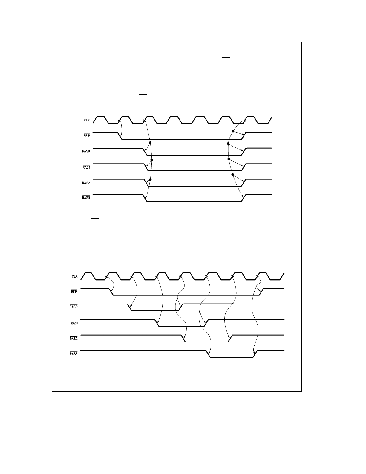
A conventional refresh cycle causes RAS0– 3 to all assert
from the first positive edge of CLK after RFIP
shown in
number of positive edges of CLK programmed have passed.
On the last positive edge, RAS
ed. This type of refresh cycle is programmed by negating
address bit R9 during programming.
Figure 16
Refresh
is asserted as
. RAS0 –3 will stay asserted until the
0–3, and RFIP will be negat-
FIGURE 16. Conventional RAS Refresh
5.2.2 Staggered RAS
A staggered refresh staggers each RAS or group of RASs
by a positive edge of CLK as shown in
ber of RAS
of CLK, is determined by the RAS
programming bits C4 – C6. If single RAS
ed during programming, then each RAS
cessive positive edges of CLK. If two RAS
lected during programming then RAS
s, which will be asserted on each positive edge
Refresh
Figure 17
, CAS configuration mode
0 and RAS1 will assert
. The num-
outputs are select-
will assert on suc-
outputs are se-
FIGURE 17. Staggered RAS Refresh
TL/F/11118– 25
on the first positive edge of CLK after RFIP
RAS
2 and RAS3 will assert on the second positive edge of
CLK after RFIP
during programming, all RAS
first positive edge of CLK after RFIP
or group of RASs will meet the programmed RAS low time
and then negate.
is asserted. If all RAS outputs were selected
outputs would assert on the
is asserted. Each RAS
is asserted.
TL/F/11118– 26
23
Page 24
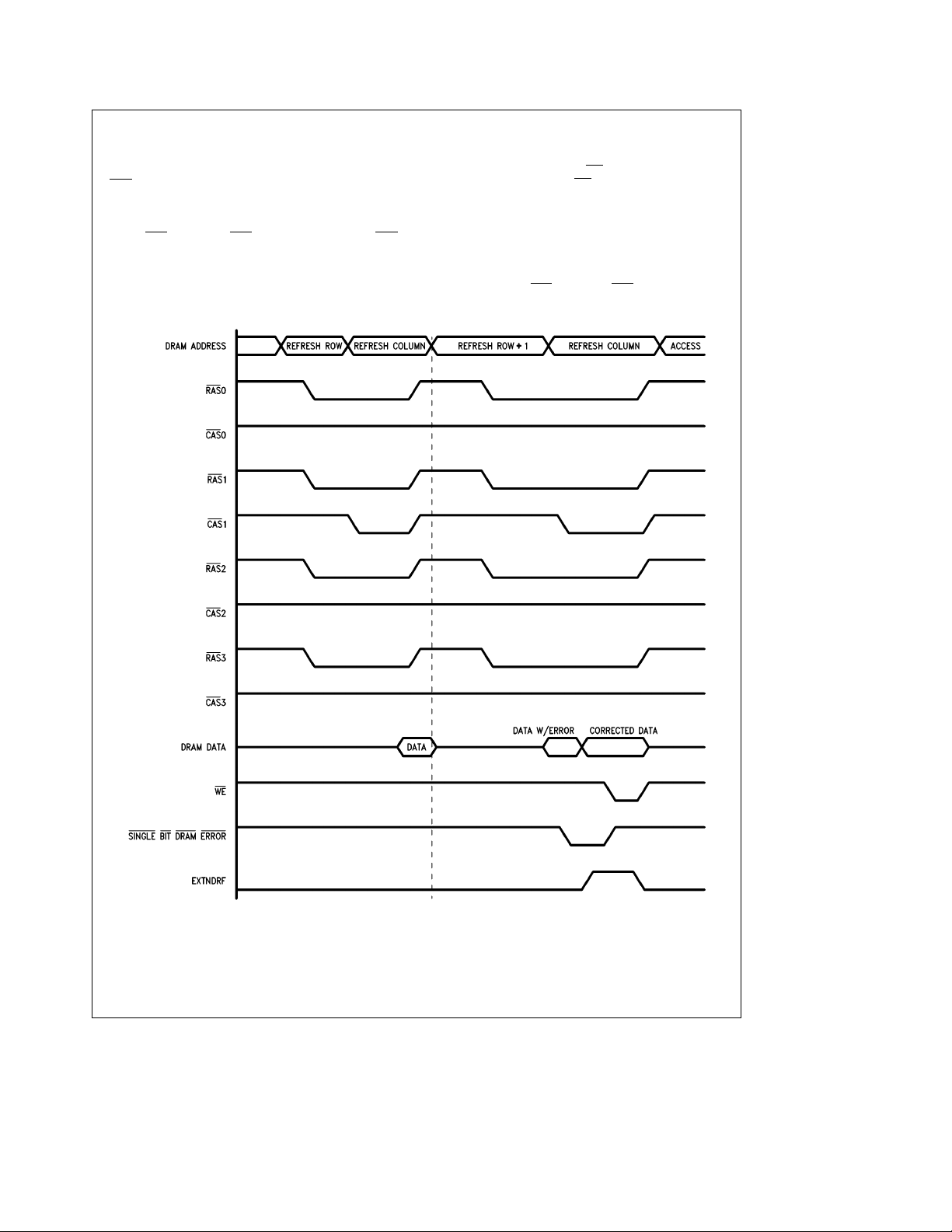
5.0 Refresh Options (Continued)
5.2.3 Error Scrubbing during Refresh
The DP8430V/31V/32V support error scrubbing during all
RAS
DRAM refreshes. Error scrubbing during refresh is selected through bits C4 – C6 with bit R9 negated during programming. Error scrubbing can not be used with staggered
refresh (see Section 8.0). Error scrubbing during refresh allows a CAS
refresh as shown in
from the DRAM array and passed through an Error Detection And Correction Chip, EDAC. If the EDAC determines
that the data contains a single bit error and corrects that
error, the refresh cycle can be extended with the input ex-
or group of CASs to assert during the all RAS
Figure 18
. This allows data to be read
tend refresh, EXTNDRF, and a read-modify-write operation
can be performed by asserting WE
the designer to ensure that WE
has a 24-bit internal refresh address counter that contains
the 11 row, 11 column and 2 bank addresses. The
DP8430V/31V have a 22-bit internal refresh address counter that contains the 10 row, 10 column and 2 bank addresses. These counters are configured as bank, column, row
with the row address as the least significant bits. The bank
counter bits are then used with the programming selection
to determine which CAS
a refresh.
or group of CASs will assert during
. It is the responsibility of
is negated. The DP8432V
FIGURE 18. Error Scrubbing during Refresh (Two Refresh Cycles Shown)
24
TL/F/11118– 27
Page 25
5.0 Refresh Options (Continued)
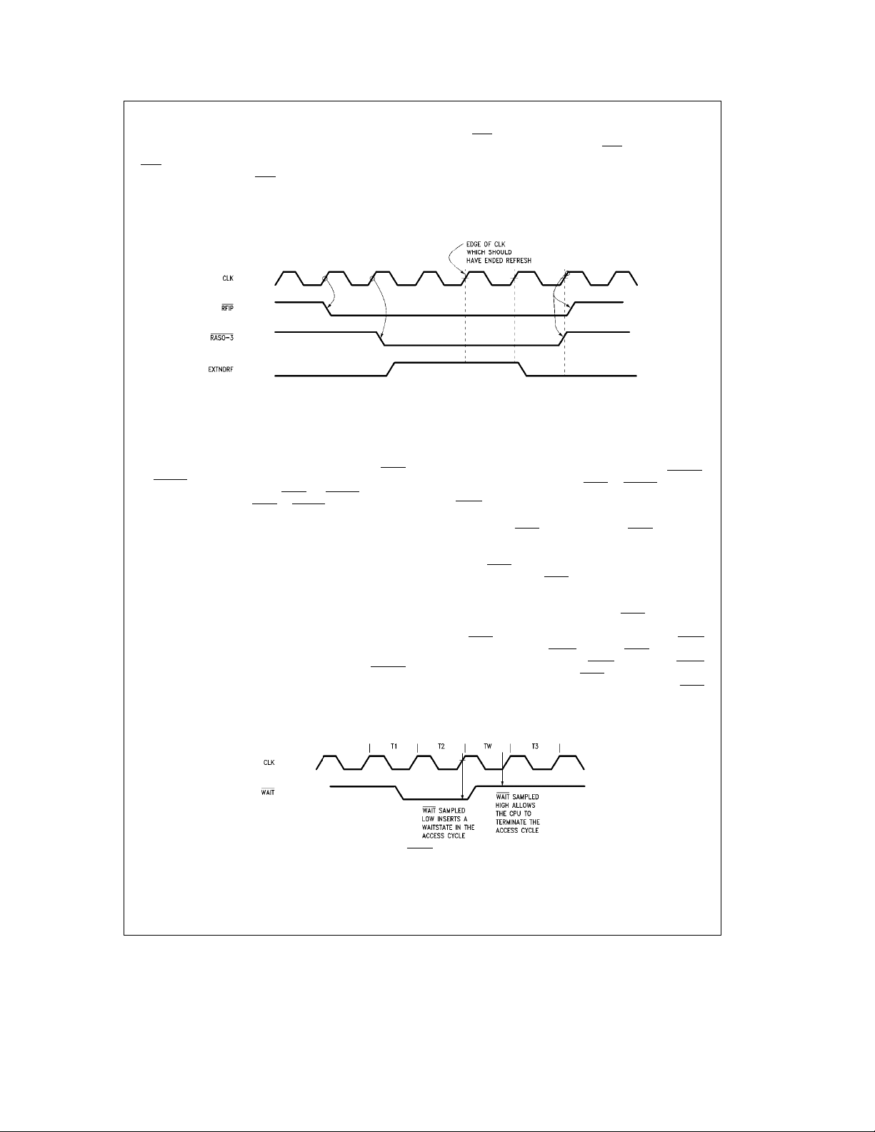
5.3 EXTENDING REFRESH
The programmed number of periods of CLK that refresh
RAS
s are asserted can be extended by one or multiple periods of CLK. Only the all RAS
bing) type of refresh can be extended. To extend a refresh
cycle, the input extend refresh, EXTNDRF, must be asserted before the positive edge of CLK that would have negated
(with or without error scrub-
all the RAS
positive edge of CLK which starts all RAS
refresh as shown in
the next positive edge of CLK and EXTNDRF will be sampled again. The refresh cycle will continue until EXTNDRF is
sampled low on a positive edge of CLK.
outputs during the refresh cycle and after the
Figure 19
. This will extend the refresh to
outputs during the
FIGURE 19. Extending Refresh with the Extend Refresh (EXTNDRF) Input
6.0 Port A Wait State Support
Wait states allow a CPU’s access cycle to be increased by
one or multiple CPU clock periods. The wait or ready input is
named differently by CPU manufacturers. However, any
CPU’s wait or ready input is compatible with either the WAIT
or DTACK output of the DP8430V/31V/32V. The user determines whether to program WAIT
which value to select for WAIT
ing upon the CPU used and where the CPU samples its wait
input during an access cycle.
The decision to terminate the CPU access cycle is directly
affected by the speed of the DRAMs used. The system designer must ensure that the data from the DRAMs will be
present for the CPU to sample or that the data has been
written to the DRAM before allowing the CPU access cycle
to terminate.
The insertion of wait states also allows a CPU’s access cycle to be extended until the DRAM access has taken place.
The DP8430V/31V/32V insert wait states into CPU access
cycles due to; guaranteeing precharge time, refresh currently in progress, user programmed wait states, the WAITIN
signal being asserted and GRANTB not being valid
(DP8432V only). If one of these events is taking place and
the CPU starts an access, the DP8430V/31V/32V will insert
wait states into the access cycle, thereby increasing the
or DTACK (R7) and
or DTACK (R2, R3) depend-
TL/F/11118– 28
length of the CPU’s access. Once the event has been completed, the DP8430V/31V/32V will allow the access to take
place and stop inserting wait states.
There are six programming bits, R2 –R7; an input, WAITIN
and an output that functions as WAIT
6.1 WAIT
With the R7 address bit negated during programming, the
user selects the WAIT
asserted by the CPU, wait states (extra clock periods) are
inserted into the current access cycle as shown in
20
completed by the CPU. WAIT
a chip selected access and is programmed to negate a
number of positive edges and/or negative levels of CLK
from the event that starts the access. WAIT
programmed to function in page/burst mode applications.
Once WAIT
inputs are negated with AREQ asserted, WAIT can be programmed to toggle, following the ECAS
is negated, ending the access, WAIT will stay negated until
the next chip selected access. For more details about WAIT
Type Output, see Application Note AN-773.
TYPE OUTPUT
output. As long as WAIT is sampled
. Once WAIT is sampled negated, the access cycle is
is negated during an access, and the ECAS
or DTACK.
Figure
is asserted at the beginning of
can also be
inputs. Once AREQ
;
FIGURE 20. WAIT Type Output
25
TL/F/11118– 29
Page 26
6.0 Port A Wait State Support (Continued)
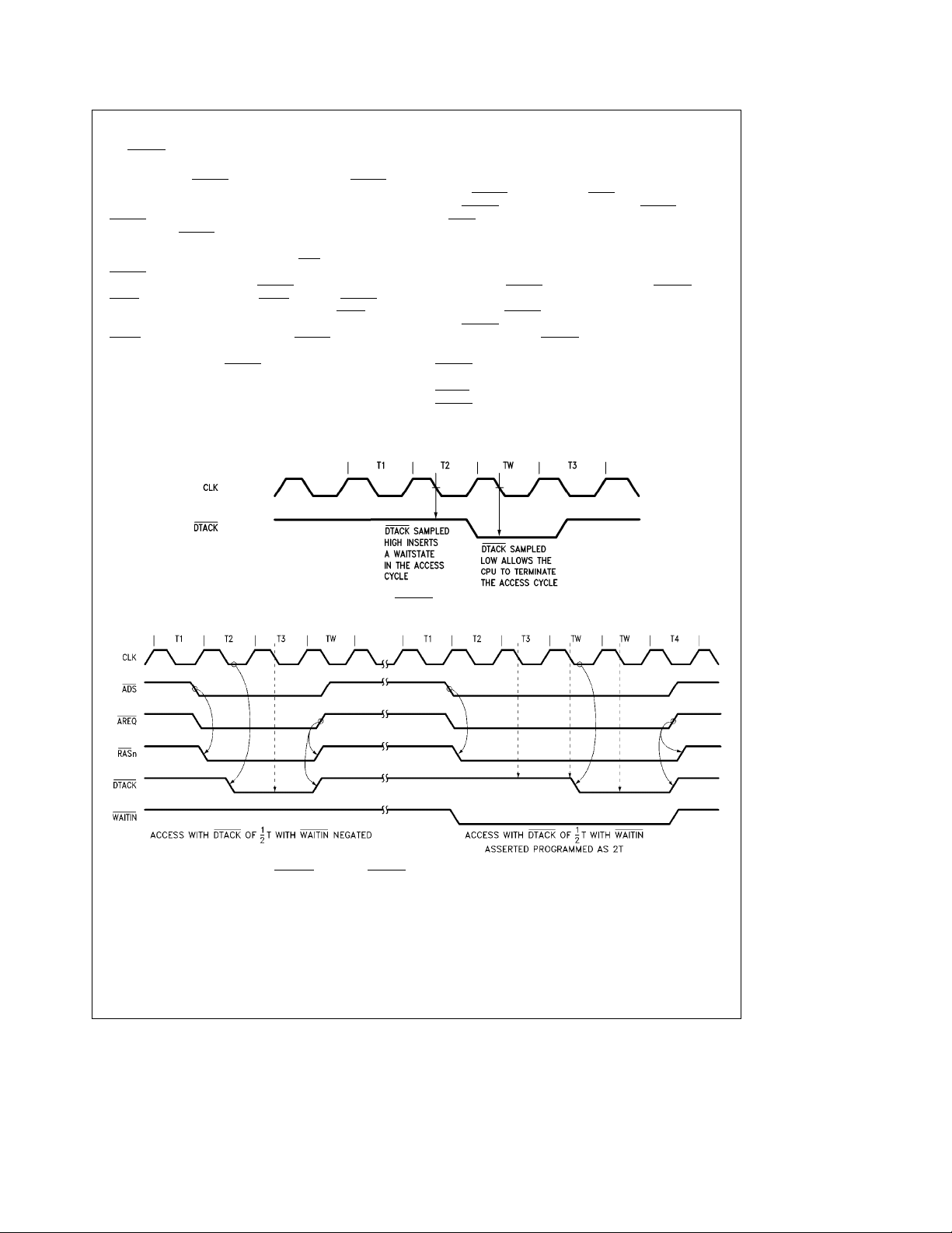
6.2 DTACK
With the R7 address bit asserted during programming, the
user selects the DTACK
sampled negated by the CPU, wait states are inserted into
the current access cycle as shown in
DTACK
by the CPU. DTACK
grammed to assert a number of positive edges and/or negative levels from the event that starts RAS
DTACK
burst mode accesses. Once DTACK
ECAS
be programmed to negate and assert from the ECAS
toggling to perform a page/burst mode operation. Once
AREQ
ed and stays negated until the next chip selected access.
For more details about DTACK
Note AN-773.
TYPE OUTPUT
type output. As long as DTACK is
is sampled asserted, the access cycle is completed
Figure 21.
, which is normally negated, is pro-
for the access.
can also be programmed to function during page/
is asserted and the
inputs are negated with AREQ asserted, DTACK can
is negated, ending the access, DTACK will be negat-
type output see Application
Once
inputs
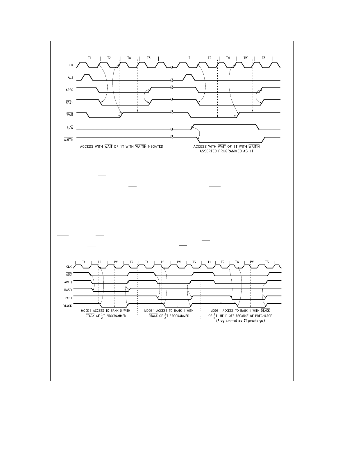
6.3 DYNAMICALLY INCREASING THE
NUMBER OF WAIT STATES
The user can increase the number of positive edges of CLK
before DTACK
input WAITIN
or WAIT
CLK. The number of edges is programmed through address
bit R6. If the user is increasing the number of positive edges
in a delay that contains a negative level, the positive edges
will be met before the negative level. For example if the user
programmed DTACK
grammed as 2T, would increase the number of positive edges resulting in DTACK
larly, WAITIN
a page/burst access. WAITIN
in systems requiring an increased number of wait states.
WAITIN
the type of access. As an example, a user could invert the
WRITE
WAITIN
1 wait state and read accesses with 2 wait states as shown
in
Figure 22b
is asserted or WAIT is negated. With the
asserted, the user can delay DTACK asserting
negating either one or two more positive edges of
of (/2T, asserting WAITIN, pro-
of 2(/2T as shown in
can increase the number of positive edges in
can be permanently asserted
can also be asserted and negated, depending on
line from the CPU and connect the output to
. This could be used to perform write accesses with
.
Figure 22a
. Simi-
FIGURE 21. DTACK Type Output
FIGURE 22a. WAITIN Example (DTACK is Sampled at the ‘‘T3’’ Falling Clock Edge)
26
TL/F/11118– 30
TL/F/11118– 31
Page 27
6.0 Port A Wait State Support (Continued)
FIGURE 22b. WAITIN Example (WAIT is Sampled at the End of ‘‘T2’’).
6.4 GUARANTEEING RAS
AND RAS
The DP8430V/31V/32V will guarantee RAS precharge time
between accesses; between refreshes; and between access and refreshes. The programming bits R0 and R1 are
used to program combinations of RAS
RAS
low time is programmed for refreshes only. During an access, the system designer guarantees the time RAS
serted through the DP8430V/31V/32V wait logic. Since inserting wait states into an access increases the length of
the CPU signals which are used to create ADS
AREQ
The precharge time is also guaranteed by the DP8430V/
31V/32V. Each RAS
PRECHARGE TIME
low time referenced by positive edges of CLK. RAS
, the time that RAS is asserted can be guaranteed.
LOW TIME
precharge time and
is as-
or ALE and
output has a separate positive edge
TL/F/11118– 32
of CLK counter. AREQ
of CLK to terminate the access. That positive edge is 1T.
The next positive edge is 2T. RAS
the programmed number of positive edges of CLK have
passed as shown in
charge time has been met, RAS
positive edge of CLK. However, since there is a precharge
counter per RAS
delayed. Precharge time before a refresh is always referenced from the access RAS
refresh asserting. After a refresh, precharge time is referenced from RAS
RAS
asserting.
is negated setup to a positive edge
will not be asserted until
Figure 23
, an access using another RAS will not be
3 negating, for the refresh, to the access
. Once the programmed pre-
will be asserted from the
negating before RAS0 for the
FIGURE 23. Guaranteeing RAS Precharge (DTACK is Sampled at the ‘‘T2’’ Falling Clock Edge)
27
TL/F/11118– 33
Page 28
7.0 RAS and CAS Configuration Modes
The DP8430V/31V/32V allow the user to configure the
DRAM array to contain one, two or four banks of DRAM.
Depending on the functions used, certain considerations
must be used when determining how to set up the DRAM
array. Programming address bits C4, C5 and C6 along with
bank selects, B0 –1, and CAS
mine which RAS
of CAS
s will be asserted during an access. Different memory schemes are described. The DP8430V/31V/32V is specified driving a heavy load of 72 DRAMs, representing four
banks of DRAM with 16-bit words and 2 parity bits. The
DP8430V/31V/32V can drive more than 72 DRAMs, but the
AC timing must be increased. Since the RAS
puts are configurable, all RAS
used for the maximum amount of drive.
or group of RASs and which CAS or group
enables, ECAS0–3, deter-
and CAS out-
and CAS outputs should be
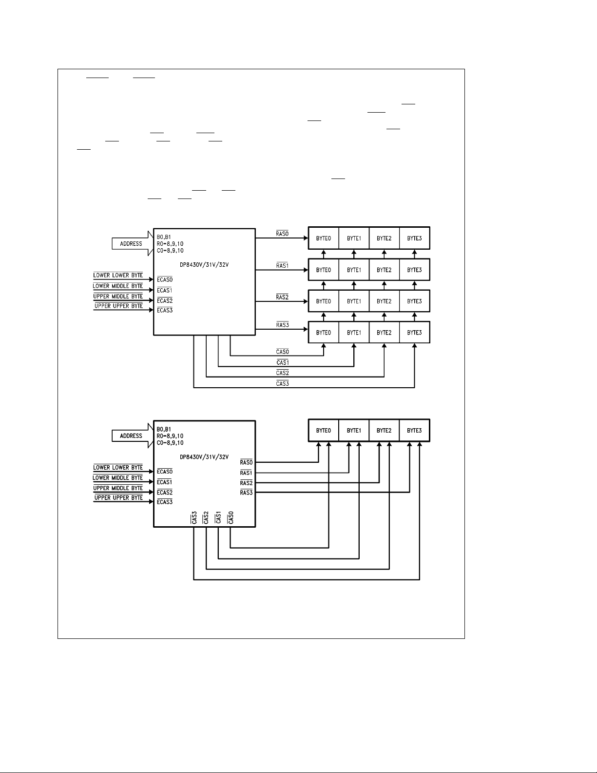
7.1 BYTE WRITING
By selecting a configuration in which all CAS
selected during an access, the ECAS
or group of CAS
size of up to 32 bits. In this case, the RAS
to select which of up to 4 banks is to be used as shown in
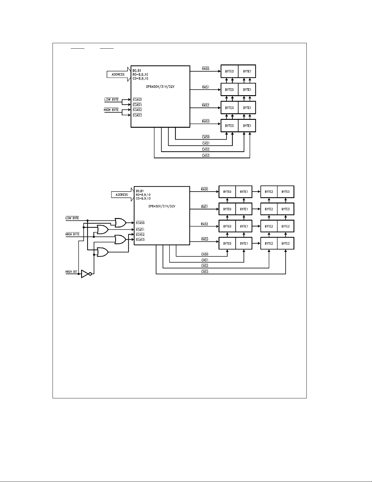
Figures 24a
the byte enables can be gated with a high order address bit
to produce four byte enables which gives an equivalent to 8
banks of 16-bit words as shown in
ry is required, each CAS
in the 16-bit word as shown in
outputs to select a byte (or bytes) in a word
and
24b
. In systems with a word size of 16 bits,
should be used to drive each nibble
inputs enable a single
Figure 24d
Figure 24c
outputs are
outputs are used
. If less memo-
.
FIGURE 24a. DRAM Array Setup for 32-Bit System (C6, C5, C4e1, 1, 0 during Programming)
FIGURE 24b. DRAM Array Setup for 32-Bit, 1 Bank System (C6, C5, C4e0, 0, 0 Allowing Error Scrubbing
or C6, C5, C4
e
0, 1, 1 No Error Scrubbing during Programming)
28
TL/F/11118– 34
TL/F/11118– 35
Page 29
7.0 RAS and CAS Configuration Modes (Continued)
FIGURE 24c. DRAM Array Setup for 16-Bit System (C6, C5, C4e1, 1, 0 during Programming)
TL/F/11118– 36
FIGURE 24d. 8 Bank DRAM Array for 16-Bit System (C6, C5, C4e1, 1, 0 during Programming)
TL/F/11118– 37
29
Page 30
7.0 RAS and CAS Configuration Modes (Continued)
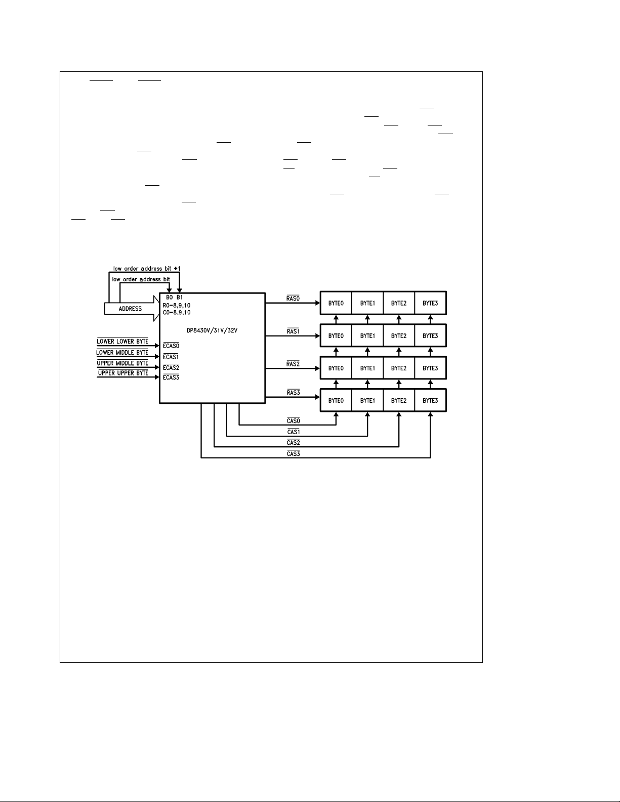
7.2 MEMORY INTERLEAVING
Memory interleaving allows the cycle time of DRAMs to be
reduced by having sequential accesses to different memory
banks. Since the DP8430V/31V/32V have separate precharge counters per bank, sequential accesses will not be
delayed if the accessed banks use different RAS
To ensure different RAS
selected where either one or two RAS
serted during an access. The bank select or selects, B0 and
B1, are then tied to the least significant address bits, causing a different group of RAS
tial access as shown in
be at least one clock period of all RAS
different RAS
CAS
’s being asserted to avoid the condition of a
before RAS refresh cycle.
outputs will be used, a mode is
s to assert during each sequen-
Figure 25
outputs will be as-
. In this figure there should
’s negated between
outputs.
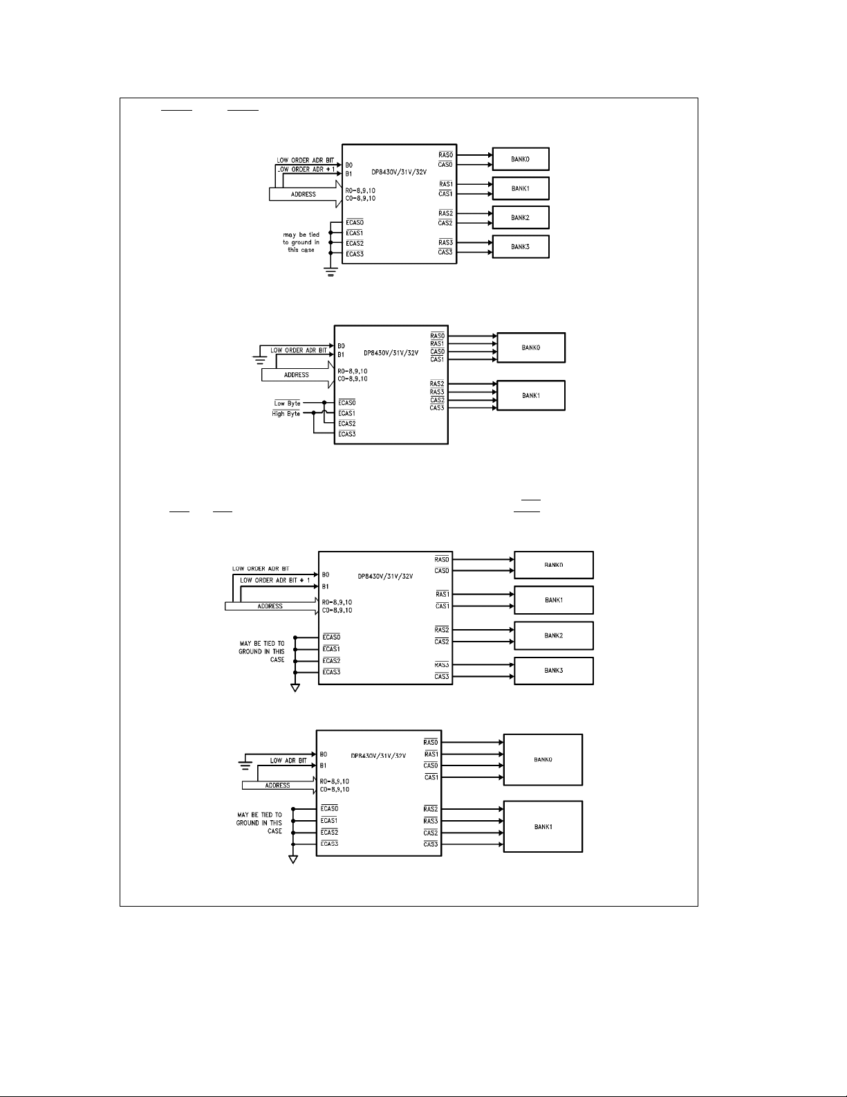
7.3 ADDRESS PIPELINING
Address pipelining allows several access RAS
serted at once. Because RAS
quires either a mode where one RAS
per bank as shown in
two CAS
writing can be accomplished in a 16-bit word system if two
RAS
s and two CASs are used per bank. In other systems,
WE
s (or external gating on the CAS outputs) must be used
to perform byte writing. If WE
and data out buffers must be used. If the array is not layed
out this way, a CAS
will cause a refresh of the DRAM, not an access. To take
full advantage of address pipelining, memory interleaving is
used. To memory interleave, the least significant address
bits should be tied to the bank select inputs to ensure that
all ‘‘back to back’’ sequential accesses are not delayed,
since different memory banks are accessed.
s can overlap, each bank re-
s are used per bank as shown in
Figure 26a
to a bank can be low before RAS, which
and one CAS are used
or where two RASs and
s are used separate data in
stobeas-
Figure 26b
. Byte
FIGURE 25. Memory Interleaving (C6, C5, C4e1, 1, 0 during Programming)
30
TL/F/11118– 38
Page 31
7.0 RAS and CAS Configuration Modes (Continued)
FIGURE 26a. DRAM Array Setup for 4 Banks Using Address Pipelining (C6, C5, C4e1, 1, 1
or C6, C5, C4
FIGURE 26b. DRAM Array Setup for Address Pipelining with 2 Banks (C6, C5, C4e1, 0, 1
or C6, C5, C4
e
0, 1, 0 (Also Allowing Error Scrubbing) during Programming)
e
0, 0, 1 (Also Allowing Error Scrubbing) during Programming)
7.4 ERROR SCRUBBING
In error scrubbing during refresh, the user selects one, two
or four RAS
and CAS outputs per bank. When performing
error detection and correction, memory is always accessed
as words. Since the CAS
individual bytes, the ECAS
in
Figures 27a
and
27b
.
TL/F/11118– 39
TL/F/11118– 40
signals are not used to select
inputs can be tied low as shown
FIGURE 27a. DRAM Array Setup for 4 Banks Using Error Scrubbing (C6, C5, C4e0, 1, 0 during Programming)
TL/F/11118– 41
FIGURE 27b. DRAM Array Setup for Error Scrubbing with 2 Banks (C6, C5, C4e0, 0, 1 during Programming)
TL/F/11118– 42
31
Page 32
7.0 RAS and CAS Configuration Modes (Continued)
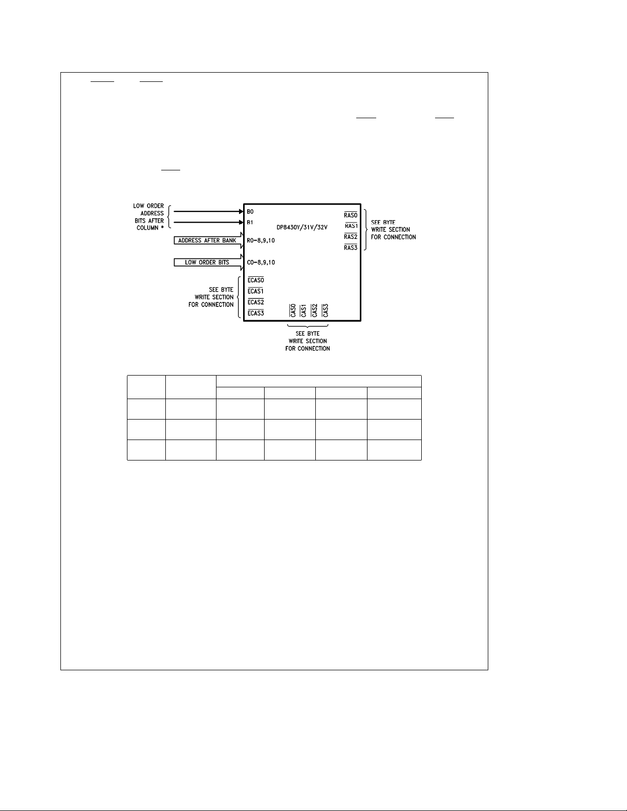
7.5 PAGE/BURST MODE
In a static column, page or burst mode system, the least
significant bits must be tied to the column address in order
to ensure that the page/burst accesses are to sequential
memory addresses, as shown in
Figure 28.
In a nibble
mode system, the least significant bits must be tied to the
highest column and row address bits in order to ensure that
sequential address bits are the ‘‘nibble’’ bits for nibble mode
accesses
*See table below for row, column & bank address bit map. A0, A1 are used for byte addressing in this example.
(Figure 28)
. The ECAS inputs may then be tog-
Addresses Nibble Mode*
Column C9,R9eA2,A3 C0– 7eA2–9 C0–8eA2–10 C0–9eA2–11
Address C0 –8
Row
Address
B0 A4 A10 A11 A12 A13
B1 A5 A11 A12 A13 A14
Assume that the least significant address bits are used for byte addressing. Given a 32-bit system A0,A1 would be
used for byte addressing.
e
X
DON’T CARE, the user can do as he pleases.
*Nibble mode values for R and C assume a system using 1 Mbit DRAMs.
XXX X X
256 Bits/Page 512 Bits/Page 1024 Bits/Page 2048 Bits/Page
e
X C8–10eX C9,10eX C10eX
FIGURE 28. Page, Static Column, Nibble Mode System
gled with the DP8430V/31V/32V’s address latches in fallthrough mode, while AREQ
can also be used to select individual bytes. When using nibble mode DRAMS, the third and fourth address bits can be
tied to the bank select inputs to perform memory interleaving. In page or static column modes, the two address bits
after the page size can be tied to the bank select inputs to
select a new bank if the page size is exceeded.
Page Mode/Static Column Mode Page Size
is asserted. The ECAS inputs
TL/F/11118– 43
e
C0–10
A2–12
32
Page 33
8.0 Test Mode
Staggered refresh in combination with the error scrubbing
mode places the DP8430V/31V/32V in test mode. In this
mode, the 24-bit refresh counter is divided into a 13-bit and
11-bit counter. During refreshes both counters are incremented to reduce test time.
9.0 DRAM Critical Timing
Parameters
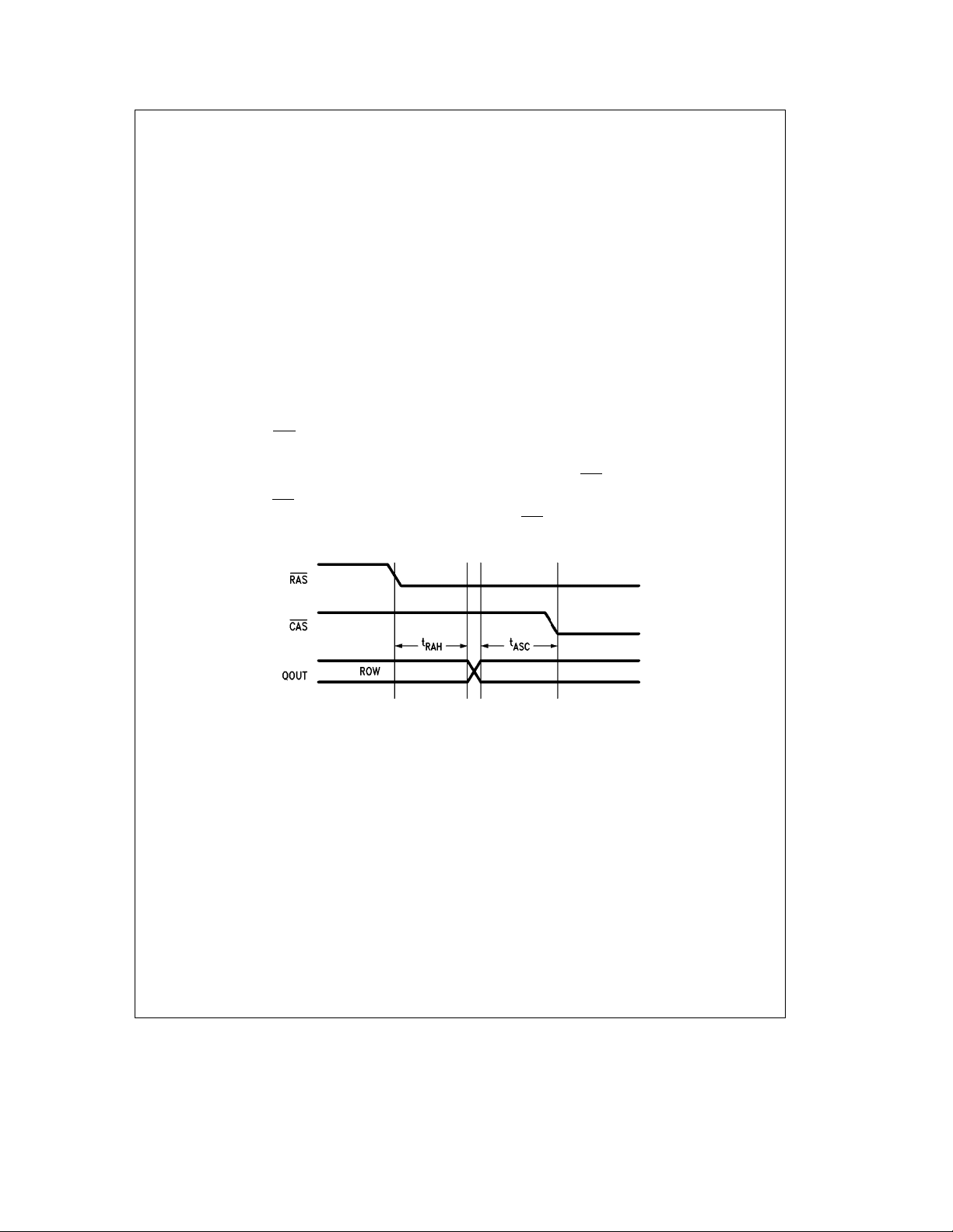
The two critical timing parameters, shown in
must be met when controlling the access timing to a DRAM
are the row address hold time, t
dress setup time, t
tain a precise internal delay line, the values of these param-
. Since the DP8430V/31V/32V con-
ASC
RAH
eters can be selected at programming time. These values
will also increase and decrease if DELCLK varies from
2 MHz.
9.1 PROGRAMMABLE VALUES OF t
The DP8430V/31V/32V allow the values of t
to be selected at programming time. For each parameter,
two choices can be selected. t
time, is measured from RAS
RAH
asserted to the row address
starting to change to the column address. The two choices
for t
are 15 ns and 25 ns, programmable through ad-
RAH
dress bit C8.
t
, the column address setup time, is measured from the
ASC
column address valid to CAS
t
are 0 ns and 10 ns, programmable through address bit
ASC
C7.
asserted. The two choices for
Figure 29
, that
, and the column ad-
AND t
RAH
RAH
ASC
and t
ASC
, the row address hold
9.2 CALCULATION OF t
RAH
AND t
ASC
There are two clock inputs to the DP8430V/31V/32V.
These two clocks, DELCLK and CLK can either be tied together to the same clock or be tied to different clocks running asynchronously at different frequencies.
The clock input, DELCLK, controls the internal delay line
and refresh request clock. DELCLK should be a multiple of
2 MHz. If DELCLK is not a multiple of 2 MHz, t
will change. The new values of t
lated by the following formulas:
If t
was programmed to equal 15 ns then t
RAH
15*(((DELCLK Divisor)* 2 MHz/(DELCLK Frequency))b1)
a
15 ns.
was programmed to equal 25 ns then t
If t
RAH
25*(((DELCLK Divisor)* 2 MHz/(DELCLK Frequency))b1)
a
25 ns.
If t
was programmed to equal 0 ns then t
ASC
((DELCLK Divisor)* 2 MHz/(DELCLK Frequency))
RAH
and t
RAH
can be calcu-
ASC
ASC
and t
RAH
RAH
e
ASC
12.5*
12.5 ns.
If t
was programmed to equal 10 ns then t
ASC
((DELCLK Divisor)* 2 MHz/(DELCLK Frequency))
ASC
e
22.5*
12.5 ns.
Since the values of t
creased, the time to CAS
and t
RAH
asserted will also increase or de-
are increased or de-
ASC
crease. These parameters can be adjusted by the following
formula:
Delay to CAS
Programmed t
e
Actual Spec.aActual t
a
Actual t
RAH
ASC
b
b
RAH
Programmed t
ASC
.
e
e
b
b
FIGURE 29. t
33
RAH
and t
ASC
TL/F/11118– 44
Page 34
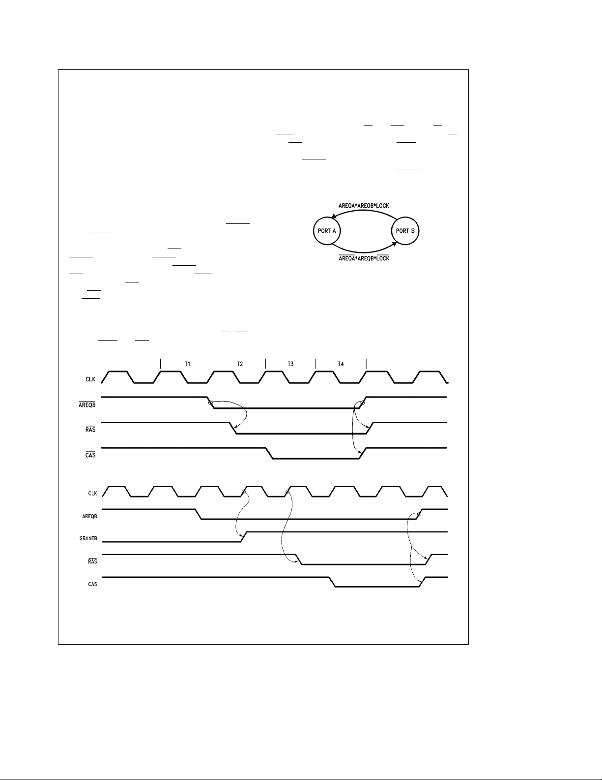
10.0 Dual Accessing (DP8432V)
The DP8432V has all the functions previously described. In
addition to those features, the DP8432V also has the capabilities to arbitrate among refresh, Port A and a second port,
Port B. This allows two CPUs to access a common DRAM
array. DRAM refresh has the highest priority followed by the
currently granted port. The ungranted port has the lowest
priority. The last granted port will continue to stay granted
even after the access has terminated, until an access request is received from the ungranted port (see
The dual access configuration assumes that both Port A
and Port B are synchronous to the system clock. If they are
not synchronous to the system clock they should be externally synchronized (Ex. By running the access requests
through several Flip-Flops, see
Figure 32a
10.1 PORT B ACCESS MODE
Port B accesses are initiated from a single input, AREQB
When AREQB
is asserted, an access request is generated.
If GRANTB is asserted and a refresh is not taking place or
precharge time is not required, RAS
AREQB
is asserted. Once AREQB is asserted, it must stay
asserted until the access is over. AREQB
RAS
as shown in
programming the CAS
yond RAS
ate ECAS
Figure 30b
. Note that if ECAS0e1 during
outputs may be held asserted (be-
n negating) by continuing to assert the appropri-
n inputs (the same as Port A accesses). If Port B
is not granted, the access will begin on the first or second
positive edge of CLK after GRANTB is asserted (See R0,
R1 programming bit definitions) as shown in
suming that Port A is not accessing the DRAM (CS
ALE and AREQ
) and RAS precharge for the particular bank
Figure 30a
).
will be asserted when
negated, negates
Figure 30c
, as-
, ADS/
has completed. It is important to note that for GRANTB to
transition to Port B, Port A must not be requesting an access at a rising clock edge (or locked) and Port B must be
requesting an access at that rising clock edge. Port A can
request an access through CS
AREQ
. Therefore during an interleaved access where CS
and ADS/ALE or CS and
and ADS/ALE become asserted before AREQ from the previous access is negated, Port A will retain GRANTB
whether AREQB
).
is asserted or not.
Since there is no chip select for Port B, AREQB must incorporate this signal. This mode of accessing is similar to Mode
1 accessing for Port A.
.
Explanation of Terms
e
AREQA
AREQB
LOCK
Chip Selected access request from Port A
e
Chip Selected access request from Port B
e
Externally controlled LOCKing of the Port
that is currently GRANTed.
FIGURE 30a. DP8432V Port A/Port B Arbitration
State Diagram. This arbitration may take place
during the ‘‘ACCESS’’ or ‘‘REFRESH’’
state (see
Figure 13
).
e
TL/F/11118– 45
0
FIGURE 30b. Access Request for Port B
FIGURE 30c. Delayed Port B Access
34
TL/F/11118– 46
TL/F/11118– 47
Page 35
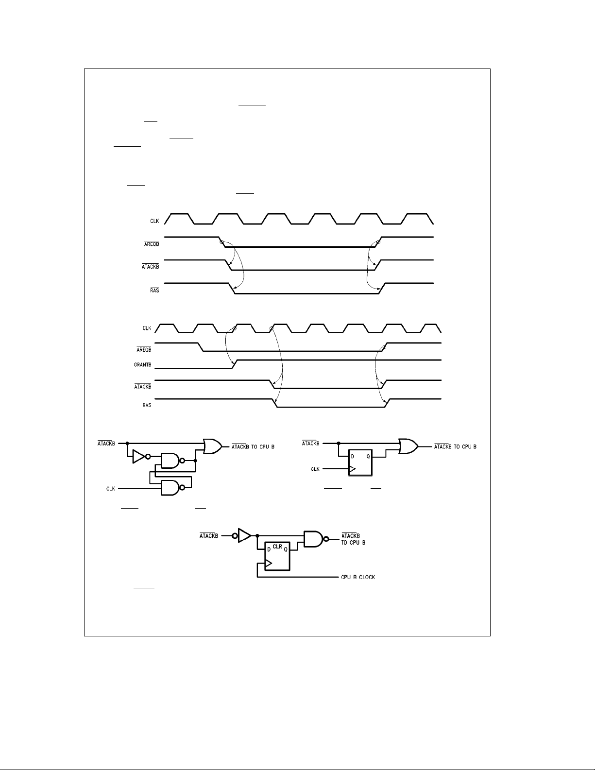
10.0 Dual Accessing (DP8432V) (Continued)
10.2 PORT B WAIT STATE SUPPORT
Advanced transfer acknowledge for Port B, ATACKB
used for wait state support for Port B. This output will be
asserted when RAS
shown in
Figures 31a
will stay asserted until AREQB
logic, ATACKB
input as shown in
for the Port B access is asserted, as
and
31b
. Once asserted, this output
is negated. With external
can be made to interface to any CPU’s wait
Figure 31c
.
10.3 COMMON PORT A AND PORT B DUAL PORT
FUNCTIONS
An input, LOCK
, and an output, GRANTB, add additional
functionality to the dual port arbitration logic. LOCK
,is
allows
Port A or Port B to lock out the other port from the DRAM.
When a Port is locked out of the DRAM, wait states will be
inserted into its access cycle until it is allowed to access
memory. GRANTB is used to multiplex the input control signals and addresses to the DP8432V.
10.3.1 GRANTB Output
The output GRANTB determines which port has current access to the DRAM array. GRANTB asserted signifies Port B
has access. GRANTB negated signifies Port A has access
to the DRAM array.
FIGURE 31a. Non-Delayed Port B Access
FIGURE 31b. Delayed Port B Access
B. Extend ATACK to 1T after RAS goes low.
TL/F/11118– 50
A. Extend ATACK to (/2T((/2 Clock) after RAS goes low.
C. Synchronize ATACKB to CPU B Clock. This is useful if CPU B runs asynchronous to the DP8432.
FIGURE 31c. Modifying Wait Logic for Port B
TL/F/11118– 48
TL/F/11118– 49
TL/F/11118– 51
TL/F/11118– 52
35
Page 36
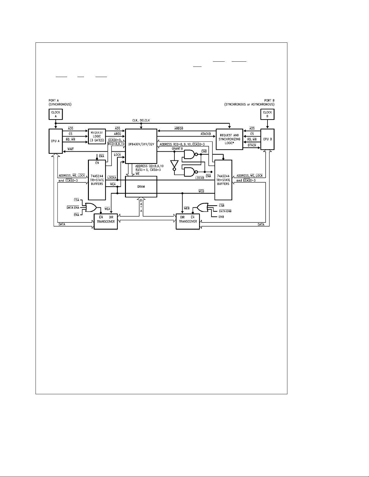
10.0 Dual Accessing (DP8432V) (Continued)
Since the DP8432V has only one set of address inputs, the
signal is used, with the addition of buffers, to allow the currently granted port’s addresses to reach the DP8432V. The
signals which need to be bufferred are R0 –10, C0 – 10,
B0–1, ECAS
common and do not have to be buffered as shown in
32a.
0–3, WE, and LOCK. All other inputs are not
Figure
If a Port, which is not currently granted, tries to access
the DRAM array, the GRANTB output will transition from a
rising clock edge from AREQ
precede the RAS
ods. GRANTB will then stay in this state until the other port
requests an access and the currently granted port is not
accessing the DRAM as shown in
for the access by one or two clock peri-
or AREQB negating and will
Figure 32b
.
*If Port B is synchronous the Request Synchronizing logic will not be required.
FIGURE 32a. Dual Accessing with the DP8432V (System Block Diagram)
TL/F/11118– 53
36
Page 37
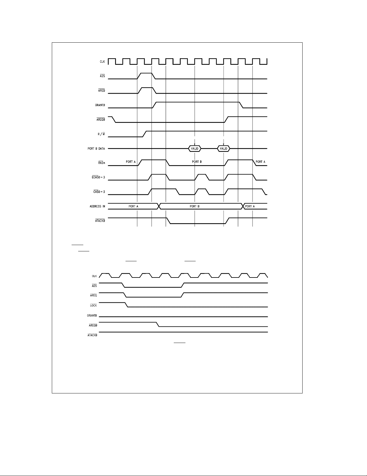
10.0 Dual Accessing (DP8432V) (Continued)
FIGURE 32b. Wait States during a Port B Access
10.3.2 LOCK
When the LOCK
can ‘‘lock out’’ the other port through the insertion of wait
states to that port’s access cycle. LOCK
Input
input is asserted, the currently granted port
does not disable
FIGURE 33. LOCK Function
refreshes, it only keeps GRANTB in the same state even if
the other port requests an access, as shown in
LOCK
can be used by either port.
37
TL/F/11118– 54
Figure 33
TL/F/11118– 55
.
Page 38
11.0 Absolute Maximum Ratings (Note 1)
If Military/Aerospace specified devices are required,
please contact the National Semiconductor Sales
Office/Distributors for availability and specifications.
Temperature under Bias ААААААААААААААААААА0
Storage Temperature АААААААААААААААААb65§Ctoa150§C
Ctoa70§C
§
All Input or Output Voltage
with Respect to GNDААААААААААААААААААА
b
0.5V toa7V
Power Dissipation@20 MHzААААААААААААААААААААААА0.5W
ESD RatingААААААААААААААААААААААААААААААААААААА2000V
Temperature Cycle АААААААААААААААААААААА300 of 0/125§C
12.0 DC Electrical Characteristics T
e
0§Ctoa70§C, V
A
e
5Vg10%, GNDe0V
CC
Symbol Parameter Conditions Min Typ Max Units
V
IH
V
IL
V
OH1
V
OL1
V
OH2
V
OL2
I
IN
I
IL ML
I
CC1
I
CC1
I
CC1
I
CC2
I
CC2
I
CC2
Logical 1 Input Voltage Tested with a Limited
Functional Pattern
Logical 0 Input Voltage Tested with a Limited
Functional Pattern
Q and WE Outputs I
Q and WE Outputs I
All Outputs except Qs, WE I
All Outputs except Qs, WE I
Input Leakage Current V
ML Input Current (Low) V
Standby Current CLK at 12 MHz (V
Standby Current CLK at 20 MHz (V
Standby Current CLK at 33 MHz (V
eb
10 mA V
OH
e
10 mA 0.5 V
OL
eb
3mA V
OH
e
3 mA 0.5 V
OL
e
VCCor GND
IN
e
GND 200 mA
IN
e
VCCor GND) 6 15 mA
IN
e
VCCor GND) 8 17 mA
IN
e
VCCor GND) 10 20 mA
IN
Supply Current CLK at 12 MHz (Inputs Active)
(I
LOAD
e
25 pF) (V
e
IN
VCCor GND)
Supply Current CLK at 20 MHz (Inputs Active)
(I
LOAD
e
25 pF) (V
e
IN
VCCor GND)
Supply Current CLK at 33 MHz (Inputs Active)
(I
LOAD
e
25 pF) (V
e
IN
VCCor GND)
2.0 V
b
0.5 0.8 V
b
1.0 V
CC
b
1.0 V
CC
b
10 10 mA
CC
a
0.5 V
30 60 mA
65 90 mA
115 150 mA
CIN* Input Capacitance fINat 1 MHz 10 pF
*CINis not 100% tested.
Note 1: ‘‘Absolute Maximum Ratings’’ are those values beyond which the safety of the device cannot be guaranteed. They are not meant to imply that the devices
should be operated at these limits. The tables of ‘‘Electrical Characteristics’’ provide conditions for actual device operation.
Note 2: Input pulse 0V to 3V; t
Note 3: AC production testing is done at 50 pF.
e
e
t
2.5 ns. Input reference point on AC measurements is 1.5V. Output reference point is 1.5V.
R
F
38
Page 39
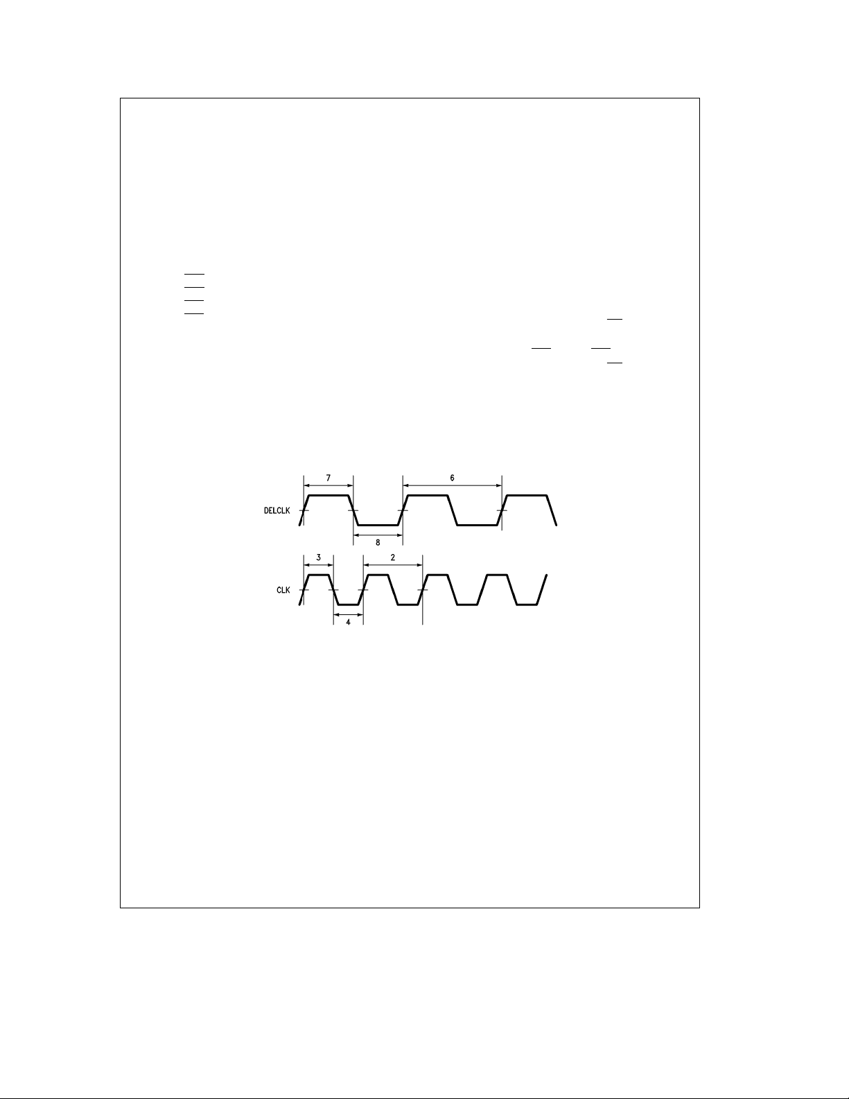
13.0 AC Timing Parameters
Two speed selections are given, the DP8430V/31V/32V-20
and the DP8430V/31V/32V-33. The differences between
the two parts are the maximum operating frequencies of the
input CLKs and the maximum delay specifications. Low frequency applications may use the ‘‘-25’’ part to gain improved timing.
The AC timing parameters are grouped into sectional numbers as shown below. These numbers also refer to the timing diagrams.
1–36 Common parameters to all modes of operation
50–56 Difference parameters used to calculate;
RAS
low time,
RAS
precharge time,
CAS
high time and
CAS
low time
100–121 Common dual access parameters used for Port
B accesses and inputs and outputs used only in
dual accessing
200–212 Refresh parameters
Note 1: ‘‘Absolute Maximum Ratings’’ are the values beyond which the safety of the device cannot be guaranteed. They are not meant to imply that the device
should be operated at these limits. The table of ‘‘Electrical Characteristics’’ provides conditions for actual device operation.
Note 2: Input pulse 0V to 3V; tR
Note 3: AC Production testing is done at 50 pF.
etFe
2.5 ns. Input reference point on AC measurements is 1.5V. Output reference points are 2.4V for High and 0.8V for Low.
300–315 Mode 0 access parameters used in both single
and dual access applications
400–416 Mode 1 access parameters used in both single
and dual access applications
450–455 Special Mode 1 access parameters which super-
sede the 400 –416 parameters when dual accessing
500–506 Programming parameters
Unless otherwise stated V
70§C, the output load capacitance is typical for 4 banks of
e
5.0Vg10%, 0kT
CC
A
18 DRAMs per bank, including trace capacitance (see Note
2).
Two different loads are specified:
e
C
50 pF loads on all outputs except
L
e
C
150 pF loads on Q0 –8, 9, 10 and WE;or
L
e
50 pF loads on all outputs except
C
H
e
C
125 pF loads on RAS0 –3 and CAS0–3 and
H
e
C
380 pF loads on Q0 –8, 9, 10 and WE.
H
k
FIGURE 34. Clock, DELCLK Timing
39
TL/F/11118– 56
Page 40
13.0 AC Timing Parameters (Continued)
Unless otherwise stated V
per bank, including trace capacitance (Note 2).
Two different loads are specified:
e
C
50 pF loads on all outputs except
L
e
C
150 pF loads on Q0 –8, 9, 10 and WE;or
L
e
5.0Vg10%, 0§CkT
CC
A
k
70§C, the output load capacitance is typical for 4 banks of 18 DRAMs
e
C
50 pF loads on all outputs except
H
e
C
125 pF loads on RAS0 –3 and CAS0–3 and
H
e
C
380 pF loads on Q0 –8, 9, 10 and WE.
H
DP8430V/31V/32V-33
C
L
C
H
Number Symbol
Common Parameter
Description
Min Max Min Max
1f
CLK
CLK Frequency 0 33 0 33
2 tCLKP CLK Period 30 30
3, 4 tCLKPW CLK Pulse Width 12 12
5 fDCLK DELCLK Frequency 12 40 12 40
6 tDCLKP DELCLK Period 25 83 25 83
7, 8 tDCLKPW DELCLK Pulse Width 12 12
9a tPRASCAS0 RAS Asserted to CAS Asserted
e
(tRAH
15 ns, tASCe0 ns)
9b tPRASCAS1 RAS Asserted to CAS Asserted
(tRAHe15 ns, tASCe10 ns)
9c tPRASCAS2 (RAS Asserted to CAS Asserted
e
(tRAH
25 ns, tASCe0 ns)
9d tPRASCAS3 (RAS Asserted to CAS Asserted
e
(tRAH
25 ns, tASCe10 ns)
30 30
40 40
40 40
50 50
10a tRAH Row Address Hold Time (tRAHe15) 15 15
10b tRAH Row Address Hold Time (tRAHe25) 25 25
11a tASC Column Address Setup Time (tASCe0) 0 0
11b tASC Column Address Setup Time (tASCe10) 10 10
12 tPCKRAS CLK High to RAS
following Precharge
Asserted
18 22
13 tPARQRAS AREQ Negated to RAS Negated 25 29
14 tPENCL ECAS0–3 Asserted to CAS Asserted 15 22
15 tPENCH ECAS0– 3 Negated to CAS Negated 14 21
16 tPARQCAS AREQ Negated to CAS Negated 36 43
17 tPCLKWH CLK to WAIT Negated 25 25
18 tPCLKDL0 CLK to DTACK Asserted
(Programmed as DTACK of 1/2, 1, 1(/2 23 23
or if WAITIN is Asserted)
19 tPEWL ECAS Negated to WAIT Asserted
during a Burst Access
29 29
20 tSECK ECAS Asserted Setup to CLK High to
Recognize the Rising Edge of CLK 13 13
during a Burst Access
40
Page 41
13.0 AC Timing Parameters (Continued)
Unless otherwise stated V
per bank, including trace capacitance (Note 2).
Two different loads are specified:
e
C
50 pF loads on all outputs except
L
e
C
150 pF loads on Q0 –8, 9, 10 and WE;or
L
e
5.0Vg10%, 0§CkT
CC
A
k
70§C, the output load capacitance is typical for 4 banks of 18 DRAMs
e
C
50 pF loads on all outputs except
H
e
C
125 pF loads on RAS0 –3 and CAS0–3 and
H
e
C
380 pF loads on Q0 –8, 9, 10 and WE.
H
DP8430V/31V/32V-33
C
L
C
H
Number Symbol
Common Parameter
Description
Min Max Min Max
21 tPEDL ECAS Asserted to DTACK
Asserted during a Burst Access 29 29
(Programmed as DTACK
22 tPEDH ECAS Negated to DTACK
Negated during a Burst Access
0)
30 30
23 tSWCK WAITIN Asserted Setup to CLK 5 5
24 tPWINWEH WIN Asserted to WE Asserted 18 28
25 tPWINWEL WIN Negated to WE Negated 18 28
26 tPAQ Row, Column Address Valid to
Q0–8, 9, 10 Valid
27 tPCINCQ COLINC Asserted to Q0–8, 9, 10
Incremented
28 tSCINEN COLINC Asserted Setup to ECAS
e
Asserted to Ensure tASC
0ns
29a tSARQCK1 AREQ, AREQB Negated Setup to CLK
High with 1 Period of Precharge
29b tSARQCK2 AREQ, AREQB Negated Setup to CLK High
withl1 Period of Precharge Programmed
14 16
25 25
11 11
20 29
24 33
30 tPAREQDH AREQ Negated to DTACK Negated 20 20
31 tPCKCAS CLK High to CAS Asserted
when Delayed by WIN
32 tSCADEN Column Address Setup to ECAS
Asserted to Guarantee tASCe0
10 11
21 28
33 tWCINC COLINC Pulse Width 10 10
34a tPCKCL0 CLK High to CAS Asserted following
Precharge (tRAH
e
15 ns, tASCe0 ns)
34b tPCKCL1 CLK High to CAS Asserted following
Precharge (tRAHe15 ns, tASCe10 ns)
34c tPCKCL2 CLK High to CAS Asserted following
Precharge (tRAH
e
25 ns, tASCe0 ns)
34d tPCKCL3 CLK High to CAS Asserted following
Precharge (tRAH
e
25 ns, tASCe10 ns)
35 tCAH Column Address Hold Time
(Interleave Mode Only)
36 tPCQR CAS Asserted to Row Address
Valid (Interleave Mode Only)
25 25
65 73
75 83
75 83
85 93
70 70
41
Page 42
13.0 AC Timing Parameters (Continued)
Unless otherwise stated V
per bank, including trace capacitance (Note 2).
Two different loads are specified:
e
C
50 pF loads on all outputs except
L
e
C
150 pF loads on Q0 –8, 9, 10 and WE;or
L
e
5.0Vg10%, 0§CkT
CC
A
k
70§C, the output load capacitance is typical for 4 banks of 18 DRAMs
e
C
50 pF loads on all outputs except
H
e
C
125 pF loads on RAS0 –3 and CAS0–3 and
H
e
C
380 pF loads on Q0 –8, 9, 10 and WE.
H
Number Symbol
Difference
Parameter Description
50 tD1 (AREQ or AREQB Negated to RAS
Negated) Minus (CLK High to RAS 99
Asserted)
51 tD2 (CLK High to Refresh RAS Negated)
Minus (CLK High to RAS Asserted)
52 tD3a (ADS Asserted to RAS Asserted
(Mode 1)) Minus (AREQ
to RAS
Negated)
Negated 4 4
53 tD3b (CLK High to RAS Asserted (Mode 0))
Minus (AREQ Negated to RAS Negated)
54 tD4 (ECAS Asserted to CAS Asserted)
Minus (ECAS
Negated to CAS Negated)
55 tD5 (CLK to Refresh RAS Asserted) Minus
(CLK to Refresh RAS
Negated)
56 tD6 (AREQ Negated to RAS Negated)
Minus (ADS
Asserted to RAS 55
Asserted (Mode 1))
DP8430V/31V/32V-33
C
L
C
H
Min Max Min Max
77
22
b
55
b
55
44
42
Page 43
13.0 AC Timing Parameters (Continued)
Unless otherwise stated V
per bank, including trace capacitance (Note 2).
Two different loads are specified:
e
C
50 pF loads on all outputs except
L
e
C
150 pF loads on Q0 –8, 9, 10 and WE;or
L
Number Symbol
e
5.0Vg10%, 0§CkT
CC
Common Dual Access
Parameter Description
k
70§C, the output load capacitance is typical for 4 banks of 18 DRAMs
A
e
C
50 pF loads on all outputs except
H
e
C
125 pF loads on RAS0 –3 and CAS0–3 and
H
e
C
380 pF loads on Q0 –8, 9, 10 and WE.
H
DP8430V/31V/32V-33
C
L
Min Max Min Max
C
H
100 tHCKARQB AREQB Negated Held from CLK High 2 2
101 tSARQBCK AREQB Asserted Setup to CLK High 5 5
102 tPAQBRASL AREQB Asserted to RAS Asserted 29 33
103 tPAQBRASH AREQB Negated to RAS Negated 24 28
105 tPCKRASG CLK High to RAS Asserted for
Pending Port B Access
37 41
106 tPAQBATKBL AREQB Asserted to ATACKB Asserted 37 37
107 tPCKATKB CLK High to ATACKB Asserted
for Pending Access
45 45
108 tPCKGH CLK High to GRANTB Asserted 28 28
109 tPCKGL CLK High to GRANTB Negated 26 26
110 tSADDCKG Row Address Setup to CLK High That
Asserts RAS
Change to Ensure tASR
111 tSLOCKCK LOCK Asserted Setup to CLK Low
to Lock Current Port
following a GRANTB 7 11
e
0 ns for Port B
44
112 tPAQATKBH AREQ Negated to ATACKB Negated 16 16
113 tPAQBCASH AREQB Negated to CAS Negated 38 45
114 tSADAQB Address Valid Setup to
AREQB
Asserted
610
116 tHCKARQG AREQ Negated Held from CLK High 5 5
117 tWAQB AREQB High Pulse Width
to Guarantee tASR
e
0ns
118a tPAQBCAS0 AREQB Asserted to CAS Asserted
(tRAHe15 ns, tASCe0 ns)
118b tPAQBCAS1 AREQB Asserted to CAS Asserted
118c tPAQBCAS2 AREQB Asserted to CAS Asserted
118d tPAQBCAS3 AREQB Asserted to CAS Asserted
(tRAH
(tRAH
(tRAH
e
e
e
15 ns, tASCe10 ns)
25 ns, tASCe0 ns)
25 ns, tASCe10 ns)
17 19
79 86
89 96
89 96
99 106
120a tPCKCASG0 CLK High to CAS Asserted
for Pending Port B Access 84 91
e
(tRAH
15 ns, tASCe0 ns)
120b tPCKCASG1 CLK High to CAS Asserted
for Pending Port B Access 94 101
e
(tRAH
15 ns, tASCe10 ns)
120c tPCKCASG2 CLK High to CAS Asserted
for Pending Port B Access 94 101
(tRAHe25 ns, tASCe0 ns)
120d tPCKCASG3 CLK High to CAS Asserted
for Pending Port B Access 104 111
e
(tRAH
25 ns, tASCe10 ns)
121 tSBADDCKG Bank Address Valid Setup to CLK
High That Starts RAS 55
for Pending Port B Access
43
Page 44
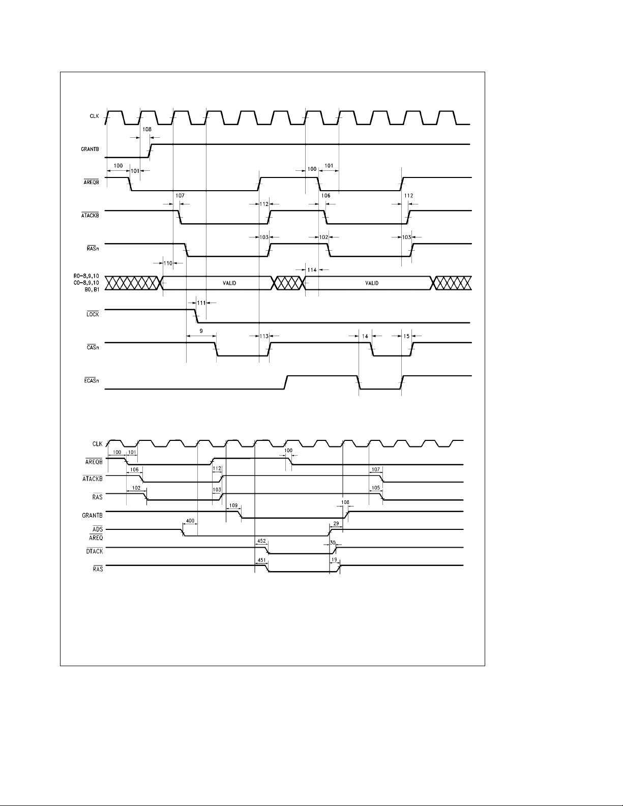
13.0 AC Timing Parameters (Continued)
FIGURE 35. 100: Dual Access Port B
FIGURE 36. 100: Port A and Port B Dual Access
44
TL/F/11118– 57
TL/F/11118– 58
Page 45
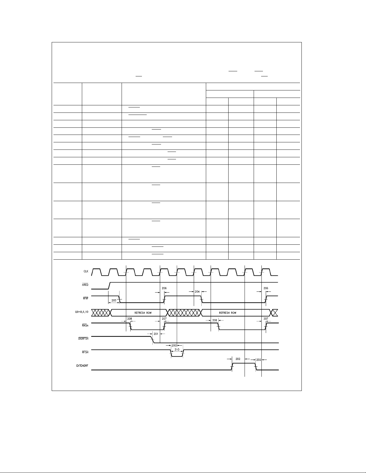
13.0 AC Timing Parameters (Continued)
Unless otherwise stated V
per bank, including trace capacitance (Note 2).
Two different loads are specified:
e
C
50 pF loads on all outputs except
L
e
C
150 pF loads on Q0 –8, 9, 10 and WE;or
L
e
5.0Vg10%, 0§CkT
CC
Number Symbol
k
70§C, the output load capacitance is typical for 4 banks of 18 DRAMs
A
Refresh Parameter
Description
e
C
50 pF loads on all outputs except
H
e
C
125 pF loads on RAS0 –3 and CAS0–3 and
H
e
C
380 pF loads on Q0 –8, 9, 10 and WE.
H
DP8430V/31V/32V-33
C
L
Min Max Min Max
C
H
200 tSRFCK RFSH Asserted Setup to CLK High 16 16
201 tSDRFCK DISRFSH Asserted Setup to CLK High 16 16
202 tSXRFCK EXTENDRF Setup to CLK High 8 8
204 tPCKRFL CLK High to RFIP Asserted 26 26
205 tPARQRF AREQ Negated to RFIP Asserted 38 38
206 tPCKRFH CLK High to RFIP Negated 41 41
207 tPCKRFRASH CLK High to Refresh RAS Negated 26 30
208 tPCKRFRASL CLK High to Refresh RAS Asserted 20 24
209a tPCKCL0 CLK High to CAS Asserted
during Error Scrubbing 64 73
e
15 ns, t
(t
RAH
ASC
e
0 ns)
209b tPCKCL1 CLK High to CAS Asserted
during Error Scrubbing 74 83
e
15 ns, t
(t
RAH
ASC
e
10 ns)
209c tPCKCL2 CLK High to CAS Asserted
during Error Scrubbing 74 83
e
25 ns, t
(t
RAH
ASC
e
0 ns)
209d tPCKCL3 CLK High to CAS Asserted
during Error Scrubbing 85 94
e
25 ns, t
(t
RAH
ASC
e
10 ns)
210 tWRFSH RFSH Pulse Width 9 9
211 tPCKRQL CLK High to RFRQ Asserted 22 22
212 tPCKRQH CLK High to RFRQ Negated 22 22
FIGURE 37. 200: Refresh Timing
45
TL/F/11118– 59
Page 46
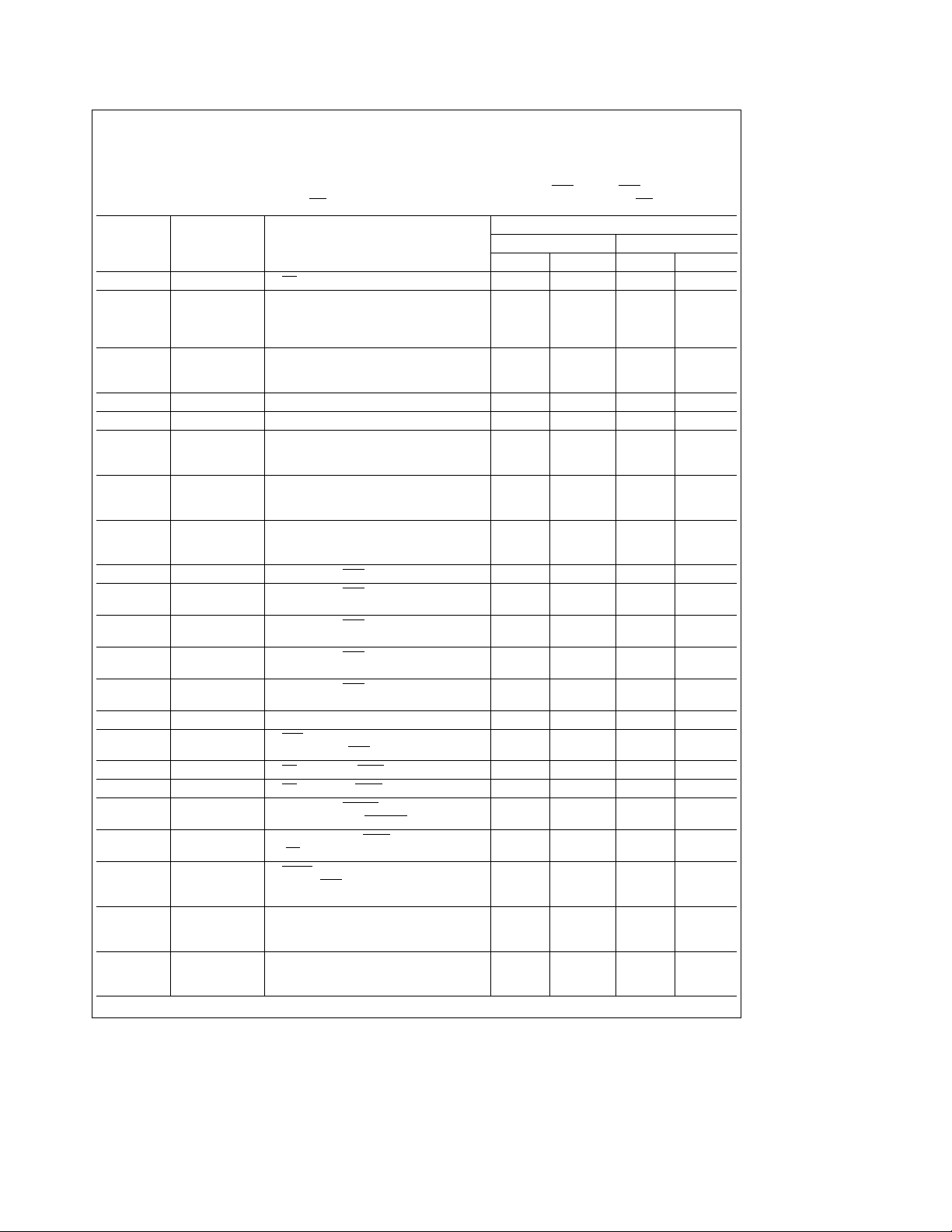
13.0 AC Timing Parameters (Continued)
Unless otherwise stated V
per bank, including trace capacitance (Note 2).
Two different loads are specified:
e
C
50 pF loads on all outputs except
L
e
C
150 pF loads on Q0 –8, 9, 10 and WE;or
L
Number Symbol
e
5.0Vg10%, 0§CkT
CC
Parameter Description
k
70§C, the output load capacitance is typical for 4 banks of 18 DRAMs
A
Mode 0 Access
e
C
50 pF loads on all outputs except
H
e
C
125 pF loads on RAS0 –3 and CAS0–3 and
H
e
C
380 pF loads on Q0 –8, 9, 10 and WE.
H
DP8430V/31V/32V-33
C
L
Min Max Min Max
C
H
300 tSCSCK CS Asserted to CLK High 8 8
301a tSALECKNL ALE Asserted Setup to CLK High
Not Using On-Chip Latches or
if Using On-Chip Latches and
11 11
B0, B1, Are Constant, Only 1 Bank
301b tSALECKL ALE Asserted Setup to CLK High,
if Using On-Chip Latches if B0, B1 20 20
Can Change, More Than One Bank
302 tWALE ALE Pulse Width 10 10
303 tSBADDCK Bank Address Valid Setup to CLK High 10 10
304 tSADDCK Row, Column Valid Setup to
CLK High to Guarantee 6 10
e
tASR
0ns
305 tHASRCB Row, Column, Bank Address
Held from ALE Negated 6 6
(Using On-Chip Latches)
306 tSRCBAS Row, Column, Bank Address
Setup to ALE Negated 1 1
(Using On-Chip Latches)
307 tPCKRL CLK High to RAS Asserted 19 23
308a tPCKCL0 CLK High to CAS Asserted
308b tPCKCL1 CLK High to CAS Asserted
308c tPCKCL2 CLK High to CAS Asserted
308d tPCKCL3 CLK High to CAS Asserted
e
(t
15 ns, t
RAH
e
(t
15 ns, t
RAH
e
(t
25 ns, t
RAH
e
(t
25 ns, t
RAH
ASC
ASC
ASC
ASC
e
e
e
e
0 ns)
10 ns)
0 ns)
10 ns)
65 72
75 82
75 82
85 92
309 tHCKALE ALE Negated Hold from CLK High 0 0
310 tSWINCK WIN Asserted Setup to CLK High
to Guarantee CAS
is Delayed
b
16
b
16
311 tPCSWL CS Asserted to WAIT Asserted 20 20
312 tPCSWH CS Negated to WAIT Negated 20 20
313 tPCLKDL1 CLK High to DTACK Asserted
(Programmed as DTACK0
)
314 tPALEWL ALE Asserted to WAIT Asserted
(CS
is Already Asserted)
27 27
21 21
315 AREQ Negated to CLK High That Starts
Access RAS to Guarantee tASRe0ns 27 31
(Non-Interleaved Mode Only)
316 tPCKCV0 CLK High to Column
Address Valid 58 67
e
(t
15 ns, t
RAH
ASC
e
0 ns)
317 tPCKCV1 CLK High to Column
Address Valid 68 75
e
(t
25 ns, t
RAH
ASC
e
0 ns)
46
Page 47
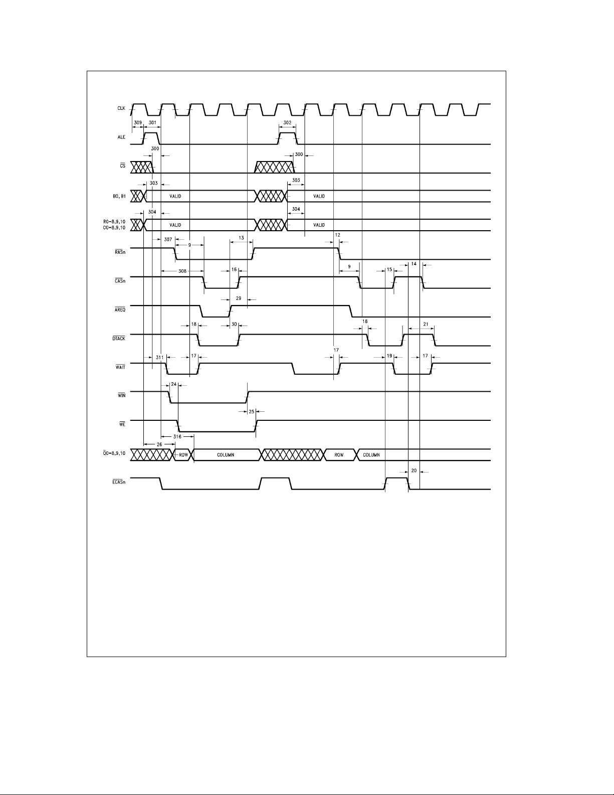
13.0 AC Timing Parameters (Continued)
FIGURE 38. 300: Mode 0 Timing
47
TL/F/11118– 60
Page 48
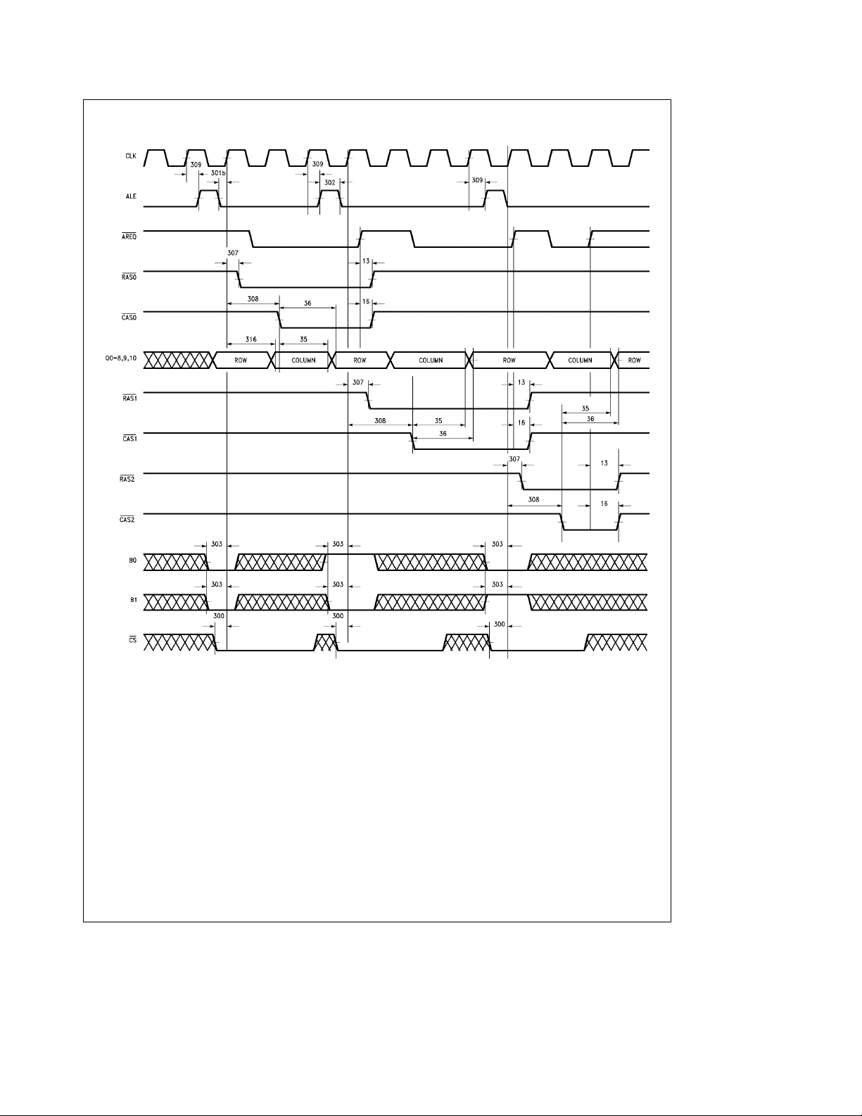
13.0 AC Timing Parameters (Continued)
(Programmed as C4e1, C5e1, C6e1)
TL/F/11118– 61
FIGURE 39. 300: Mode 0 Interleaving
48
Page 49
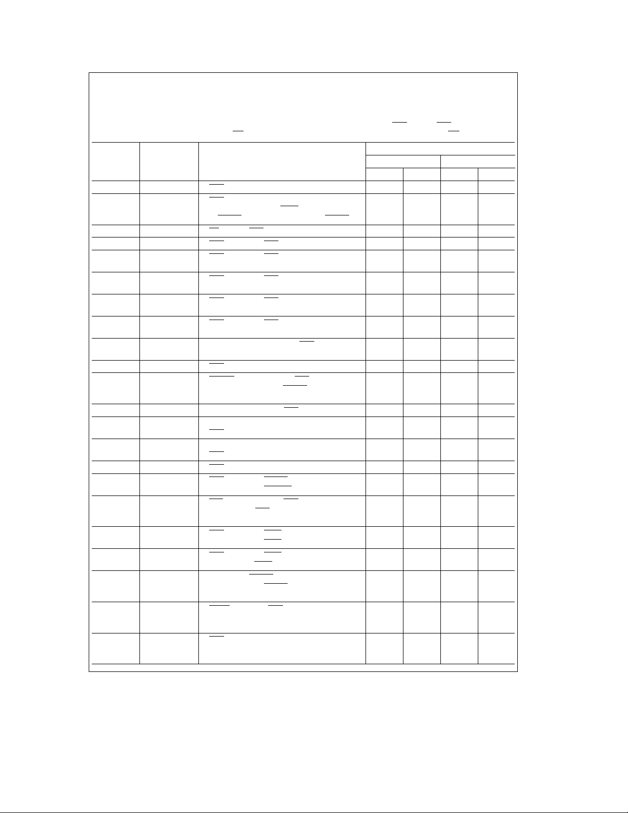
13.0 AC Timing Parameters (Continued)
Unless otherwise stated V
per bank, including trace capacitance (Note 2).
Two different loads are specified:
e
C
50 pF loads on all outputs except
L
e
C
150 pF loads on Q0 –8, 9, 10 and WE;or
L
Number Symbol
e
5.0Vg10%, 0§CkT
CC
Parameter Description
k
70§C, the output load capacitance is typical for 4 banks of 18 DRAMs
A
e
C
50 pF loads on all outputs except
H
e
C
125 pF loads on RAS0 –3 and CAS0–3 and
H
e
C
380 pF loads on Q0 –8, 9, 10 and WE.
H
Mode 1 Access
DP8430V/31V/32V-33
C
L
Min Max Min Max
C
H
400a tSADSCK1 ADS Asserted Setup to CLK High 9 9
400b tSADSCKW ADS Asserted Setup to CLK
(to Guarantee Correct WAIT
19 19
or DTACK Output; Doesn’t Apply for DTACK0)
401 tSCSADS CS Setup to ADS Asserted 4 4
402 tPADSRL ADS Asserted to RAS Asserted 20 24
403a tPADSCL0 ADS Asserted to CAS Asserted
e
(tRAH
15 ns, tASCe0 ns)
403b tPADSCL1 ADS Asserted to CAS Asserted
(tRAHe15 ns, tASCe10 ns)
403c tPADSCL2 ADS Asserted to CAS Asserted
e
(tRAH
25 ns, tASCe0 ns)
403d tPADSCL3 ADS Asserted to CAS Asserted
e
(tRAH
25 ns, tASCe10 ns)
404 tSADDADS Row Address Valid Setup to ADS
Asserted to Guarantee tASR
e
0ns
611
70 77
80 87
80 87
90 97
405 tHCKADS ADS Negated Held from CLK High 0 0
406 tSWADS WAITIN Asserted Setup to ADS
Asserted to Guarantee DTACK000
Is Delayed
407 tSBADAS Bank Address Setup to ADS Asserted 6 6
408 tHASRCB Row, Column, Bank Address Held from
ADS Asserted (Using On-Chip Latches)
409 tSRCBAS Row, Column, Bank Address Setup to
Asserted (Using On-Chip Latches)
ADS
66
11
410 tWADSH ADS Negated Pulse Width 12 17
411 tPADSD ADS Asserted to DTACK Asserted
(Programmed as DTACK0
)
29 29
412 tSWINADS WIN Asserted Setup to ADS Asserted
(to Guarantee CAS
Delayed during
b
10
b
10
Writes Accesses)
413 tPADSWL0 ADS Asserted to WAIT Asserted
(Programmed as WAIT
0, Delayed Access)
414 tPADSWL1 ADS Asserted to WAIT Asserted
(Programmed WAIT
1/2 or 1)
19 19
22 22
415 tPCLKDL1 CLK High to DTACK Asserted
(Programmed as DTACK0, 27 27
Delayed Access)
416 AREQ Negated to ADS Asserted
e
to Guarantee tASR
0ns 27 29
(Non Interleaved Mode Only)
417 tPADSCV0 ADS Asserted to Column
Address Valid 51 60
e
(t
15 ns, t
RAH
ASC
e
0 ns)
49
Page 50
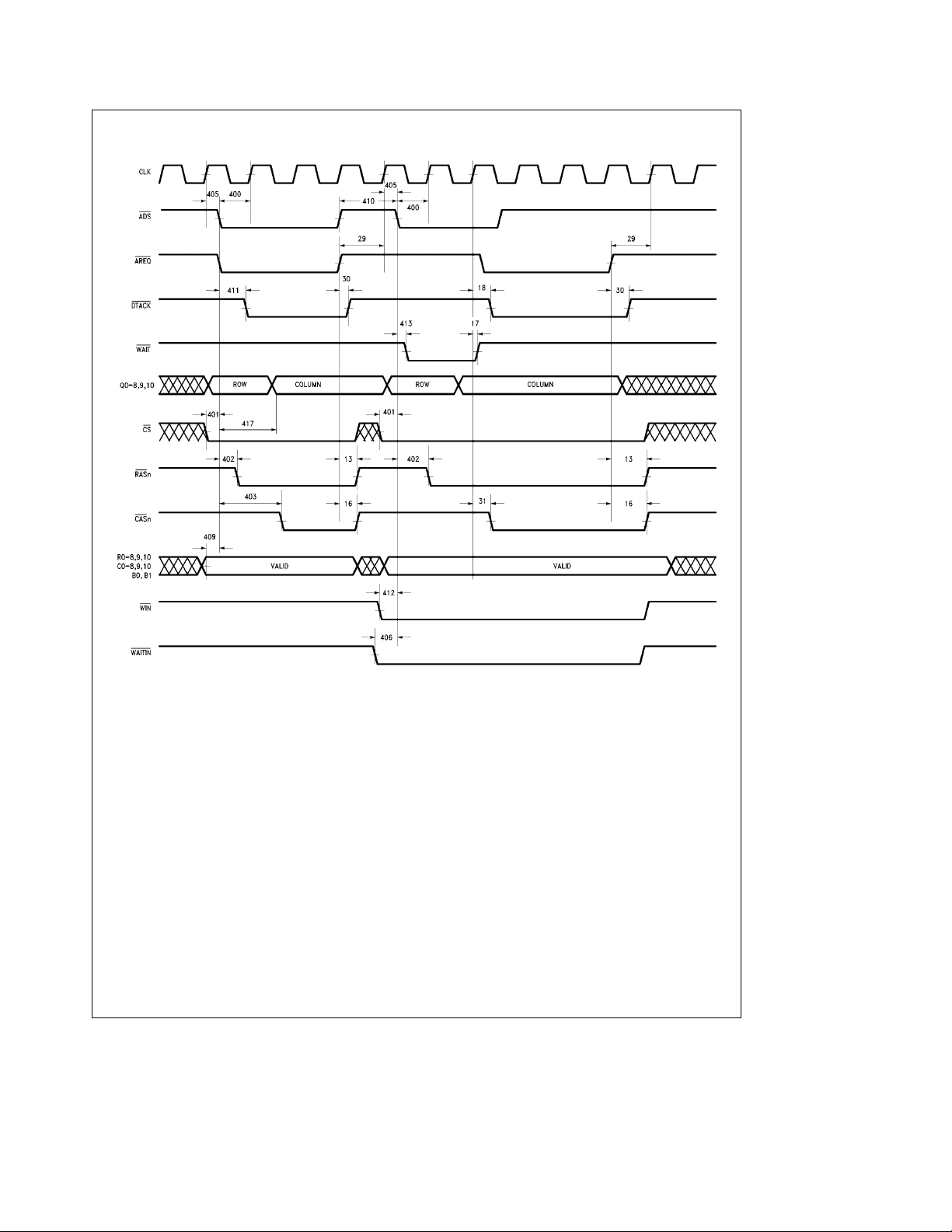
13.0 AC Timing Parameters (Continued)
FIGURE 40. 400: Mode 1 Timing
50
TL/F/11118– 62
Page 51
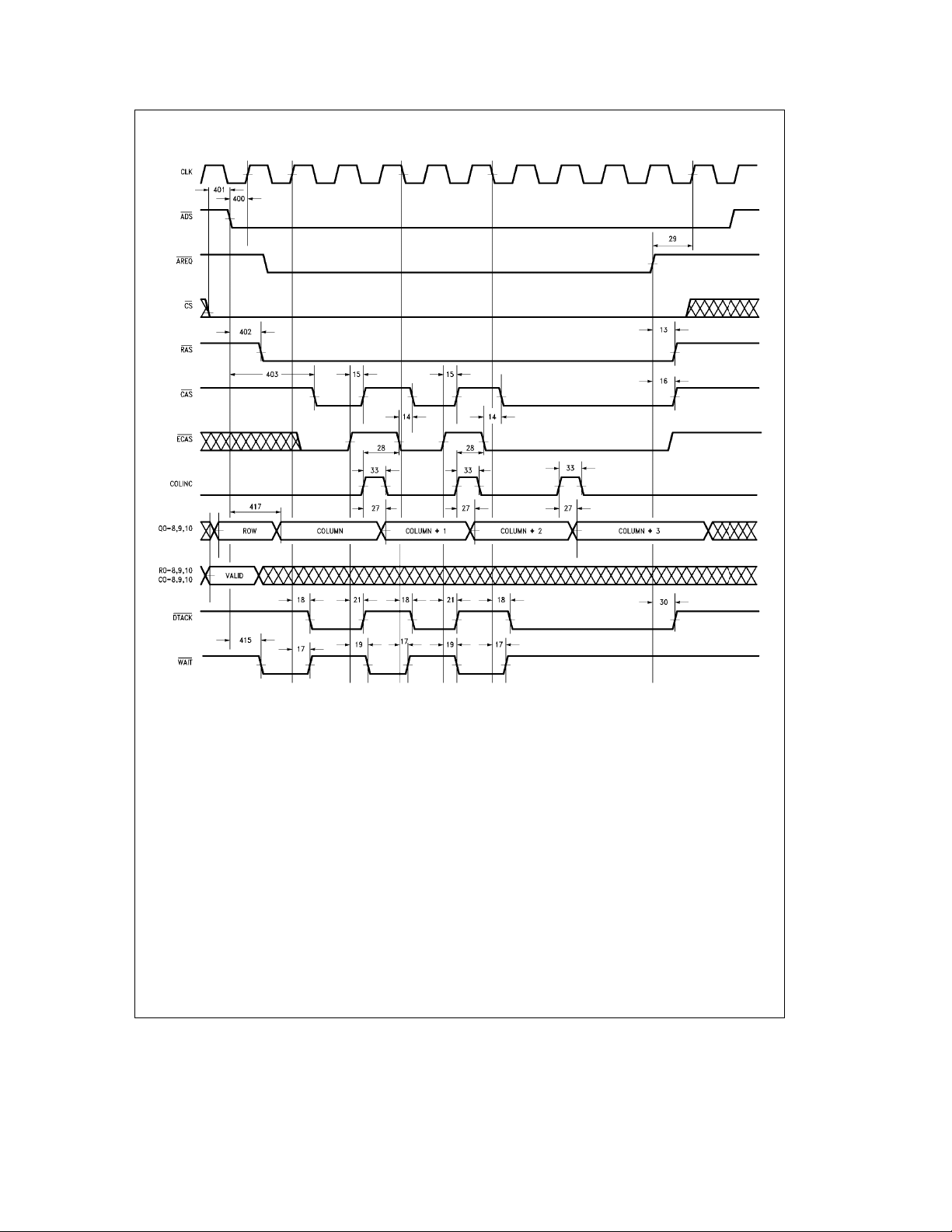
13.0 AC Timing Parameters (Continued)
FIGURE 41. 400: COLINC Page/Static Column Access Timing
51
TL/F/11118– 63
Page 52
13.0 AC Timing Parameters (Continued)
Unless otherwise stated V
per bank, including trace capacitance (Note 2).
Two different loads are specified:
e
C
50 pF loads on all outputs except
L
e
C
150 pF loads on Q0 –8, 9, 10 and WE;or
L
Number Symbol
e
5.0Vg10%, 0§CkT
CC
Mode 1 Dual Access
Parameter Description
k
70§C, the output load capacitance is typical for 4 banks of 18 DRAMs
A
e
C
50 pF loads on all outputs except
H
e
C
125 pF loads on RAS0 –3 and CAS0–3 and
H
e
C
380 pF loads on Q0 –8, 9, 10 and WE.
H
DP8430V/31V/32V-33
C
L
Min Max Min Max
450 tSADDCKG Row Address Setup to CLK High That
Asserts RAS
Port Change to Ensure tASR
451 tPCKRASG CLK High to RAS Asserted
for Pending Access
452 tPCLKDL2 CLK to DTACK Asserted for Delayed
Accesses (Programmed as DTACK
following a GRANTB 10 12
e
0ns
30 34
0)
37 37
453a tPCKCASG0 CLK High to CAS Asserted
for Pending Access 81 88
(t
RAH
e
15 ns, t
ASC
e
0 ns)
453b tPCKCASG1 CLK High to CAS Asserted
for Pending Access 91 98
(t
RAH
e
15 ns, t
ASC
e
10 ns)
453c tPCKCASG2 CLK High to CAS Asserted
for Pending Access 91 98
(t
RAH
e
25 ns, t
ASC
e
0 ns)
453d tPCKCASG3 CLK High to CAS Asserted
for Pending Access 101 108
e
(t
25 ns, t
RAH
454 tSBADDCKG Bank Address Valid Setup to CLK High
that Asserts RAS
e
10 ns)
ASC
for Pending Access
33
455 tSADSCK0 ADS Asserted Setup to CLK High 8 8
C
H
52
Page 53
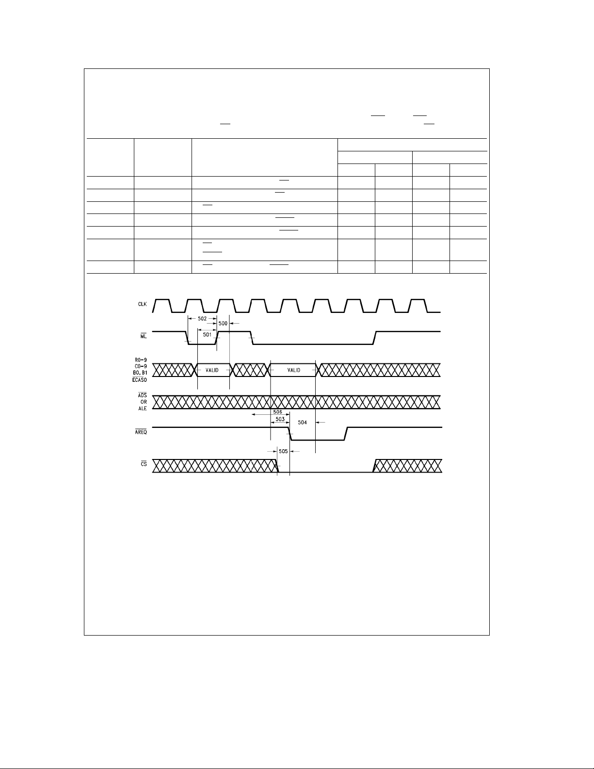
13.0 AC Timing Parameters (Continued)
Unless otherwise stated V
per bank, including trace capacitance (Note 2).
Two different loads are specified:
e
C
50 pF loads on all outputs except
L
e
C
150 pF loads on Q0 –8, 9, 10 and WE;or
L
e
5.0Vg10%, 0§CkT
CC
A
k
70§C, the output load capacitance is typical for 4 banks of 18 DRAMs
e
C
50 pF loads on all outputs except
H
e
C
125 pF loads on RAS0 –3 and CAS0–3 and
H
e
C
380 pF loads on Q0 –8, 9, 10 and WE.
H
DP8430V/31V/32V-33
C
L
Number Symbol
Programming
Parameter Description
Min Max Min Max
500 tHMLADD Mode Address Held from ML Negated 6 6
501 tSADDML Mode Address Setup to ML Negated 6 6
502 tWML ML Pulse Width 12 12
503 tSADAQML Mode Address Setup to AREQ Asserted 0 0
504 tHADAQML Mode Address Held from AREQ Asserted 30 30
505 tSCSARQ CS Asserted Setup to
AREQ
Asserted
66
506 tSMLARQ ML Asserted Setup to AREQ Asserted 6 6
C
H
FIGURE 42. 500: Programming
53
TL/F/11118– 64
Page 54

14.0 DP8430V/31V/32V User Hints
1. All inputs to the DP8430V/31V/32V should be tied high,
low or the output of some other device.
Note: One signal is active high. COLINC (EXTNDRF) should be tied low
to disable.
2. Each ground on the DP8430V/31V/32V must be decou-
pled to the closest on-chip supply (V
ramic capacitor. This is necessary because these
grounds are kept separate inside the DP8430V/31V/32V.
The decoupling capacitors should be placed as close as
possible with short leads to the ground and supply pins of
the DP8430V/31V/32V.
3. The output called ‘‘CAP’’ should have a 0.1 mF capacitor
to ground.
4. The DP8430V/31V/32V has 20X series damping resis-
tors built into the output drivers of RAS
and WE
/RFRQ. Space should be provided for external
damping resistors on the printed circuit board (or wirewrap board) because they may be needed. The value of
these damping resistors (if needed) will vary depending
upon the output, the capacitance of the load, and the
characteristics of the trace as well as the routing of the
trace. The value of the damping resistor also may vary
between the wire-wrap board and the printed circuit
board. To determine the value of the series damping resistor it is recommended to use an oscilloscope and look
at the furthest DRAM from the DP8430V/31V/32V. The
undershoot of RAS
, CAS,WEand the addresses should
be kept to less than 0.5V below ground by varying the
value of the damping resistor. The damping resistors
should be placed as close as possible with short leads to
the driver outputs of the DP8430V/31V/32V.
5. The circuit board must have a good V
plane connection. If the board is wire-wrapped, the V
and ground pins of the DP8430V/31V/32V, the DRAM
associated logic and buffer circuitry must be soldered to
the V
and ground planes.
CC
) with 0.1 mF ce-
CC
, CAS, address
and ground
CC
CC
6. The traces from the DP8430V/31V/32V to the DRAM
should be as short as possible.
7. Parameter Changes due to Loading
All A.C. parameters are specified with the equivalent load
capacitances, including traces, of 64 DRAMs organized
as 4 banks of 18 DRAMs each. Maximums are based on
worst-case conditions. If an output load changes then the
A.C. timing parameters associated with that particular
output must be changed. For example, if we changed our
output load to
e
C
250 pF loads on RAS0 –3 and CAS0–3
e
C
760 pF loads on Q0 –9 and WE
we would have to modify some parameters (not all calculated here)
$308a clock to CAS
e
(t
15 ns, t
RAH
A ratio can be used to figure out the timing change per
ASC
asserted
e
0 ns)
change in capacitance for a particular parameter by using
the specifications and capacitances from heavy and light
load timing.
$308a w/Heavy Loadb$308a w/Light Load
e
Ratio
79 nsb72 ns
e
125 pFb50 pF
$308a (actual)
CH(CAS)bCL(CAS)
7ns
e
e
(capacitance difference
75 pF
c
ratio)a$308a (specified)
e
(250 pFb125 pF)
e
11.7 nsa79 ns
e
90.7 ns@250 pF load
7ns
75 pF
a
79 ns
54
Page 55

55
Page 56
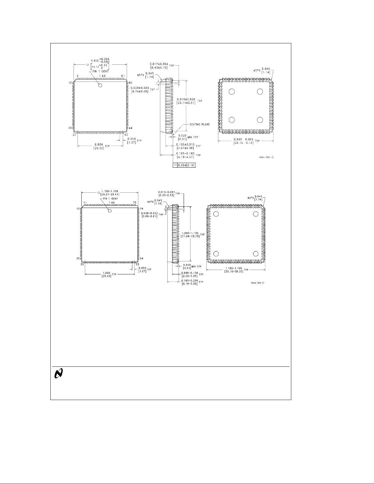
Physical Dimensions inches (millimeters)
Order Number DP8430V-33 or DP8431V-33
Plastic Chip Carrier (V)
NS Package Number V68A
256k/1M/4M Dynamic RAM Controller/Drivers
DP8430V/31V/32V-33 microCMOS Programmable
Plastic Chip Carrier (V)
Order Number DP8432V-33
NS Package Number V84ALIFE SUPPORT POLICY
NATIONAL’S PRODUCTS ARE NOT AUTHORIZED FOR USE AS CRITICAL COMPONENTS IN LIFE SUPPORT
DEVICES OR SYSTEMS WITHOUT THE EXPRESS WRITTEN APPROVAL OF THE PRESIDENT OF NATIONAL
SEMICONDUCTOR CORPORATION. As used herein:
1. Life support devices or systems are devices or 2. A critical component is any component of a life
systems which, (a) are intended for surgical implant support device or system whose failure to perform can
into the body, or (b) support or sustain life, and whose be reasonably expected to cause the failure of the life
failure to perform, when properly used in accordance support device or system, or to affect its safety or
with instructions for use provided in the labeling, can effectiveness.
be reasonably expected to result in a significant injury
to the user.
National Semiconductor National Semiconductor National Semiconductor National Semiconductor National Semiconductores National Semiconductor
Corporation GmbH Japan Ltd. Hong Kong Ltd. Do Brazil Ltda. (Australia) Pty, Ltd.
2900 Semiconductor Drive Livry-Gargan-Str. 10 Sumitomo Chemical 13th Floor, Straight Block, Rue Deputado Lacorda Franco Building 16
P.O. Box 58090 D-82256 F4urstenfeldbruck Engineering Center Ocean Centre, 5 Canton Rd. 120-3A Business Park Drive
Santa Clara, CA 95052-8090 Germany Bldg. 7F Tsimshatsui, Kowloon Sao Paulo-SP Monash Business Park
Tel: 1(800) 272-9959 Tel: (81-41) 35-0 1-7-1, Nakase, Mihama-Ku Hong Kong Brazil 05418-000 Nottinghill, Melbourne
TWX: (910) 339-9240 Telex: 527649 Chiba-City, Tel: (852) 2737-1600 Tel: (55-11) 212-5066 Victoria 3168 Australia
National does not assume any responsibility for use of any circuitry described, no circuit patent licenses are implied and National reserves the right at any time without notice to change said circuitry and specifications.
Fax: (81-41) 35-1 Ciba Prefecture 261 Fax: (852) 2736-9960 Telex: 391-1131931 NSBR BR Tel: (3) 558-9999
Tel: (043) 299-2300 Fax: (55-11) 212-1181 Fax: (3) 558-9998
Fax: (043) 299-2500
 Loading...