

Page 1
TL/F/9579
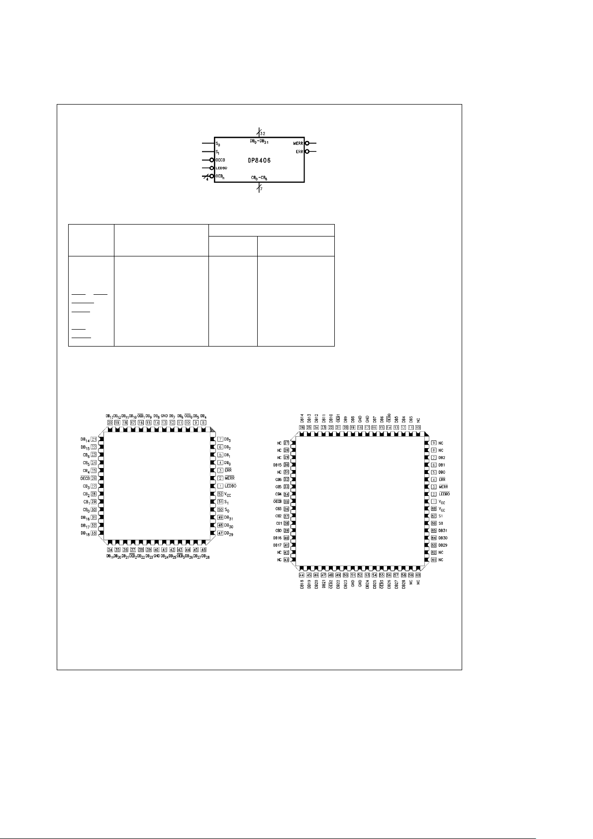
DP8406 (54F/74F632) 32-Bit Parallel Error Detection and Correction Circuit
May 1991
DP8406 (54F/74F632)
32-Bit Parallel Error Detection and Correction Circuit
General Description
The DP8406 device is a 32-bit parallel error detection and
correction circuit (EDAC) in a 52-pin or 68-pin package. The
EDAC uses a modified Hamming code to generate a 7-bit
check word from a 32-bit data word. This check word is
stored along with the data word during the memory write
cycle. During the memory read cycle, the 39-bit words from
memory are processed by the EDAC to determine if errors
have occurred in memory.
Single-bit errors in the 32-bit data word are flagged and corrected.
Single-bit errors in the 7-bit check word are flagged, and the
CPU sends the EDAC through the correction cycle even
though the 32-bit data word is not in error. The correction
cycle will simply pass along the original 32-bit data word in
this case and produce error syndrome bits to pinpoint the
error-generating location.
Dual-bit errors are flagged but not corrected. These errors
may occur in any two bits of the 39-bit word from memory
(two errors in the 32-bit data word, two errors in the 7-bit
check word, or one error in each word). The gross-error
condition of all LOWs or all HIGHs from memory will be
detected. Otherwise, errors in three or more bits of the
39-bit word are beyond the capabilities of these devices to
detect.
Read-modify-write (byte-control) operations can be performed by using output latch enable, LEDBO
, and the indi-
vidual OEB
0
through OEB3byte control pins.
Diagnostics are performed on the EDACs by controls and
internal paths that allow the user to read the contents of the
Data Bit and Check Bit input latches. These will determine if
the failure occurred in memory or in the EDAC.
Features
Y
Detects and corrects single-bit errors
Y
Detects and flags dual-bit errors
Y
Built-in diagnostic capability
Y
Fast write and read cycle processing times
Y
Byte-write capability
Y
Guaranteed 4000V minimum ESD protection
Y
Fully pin and function compatible with TI’s
SN74ALS632A thru SN74ALS635 series
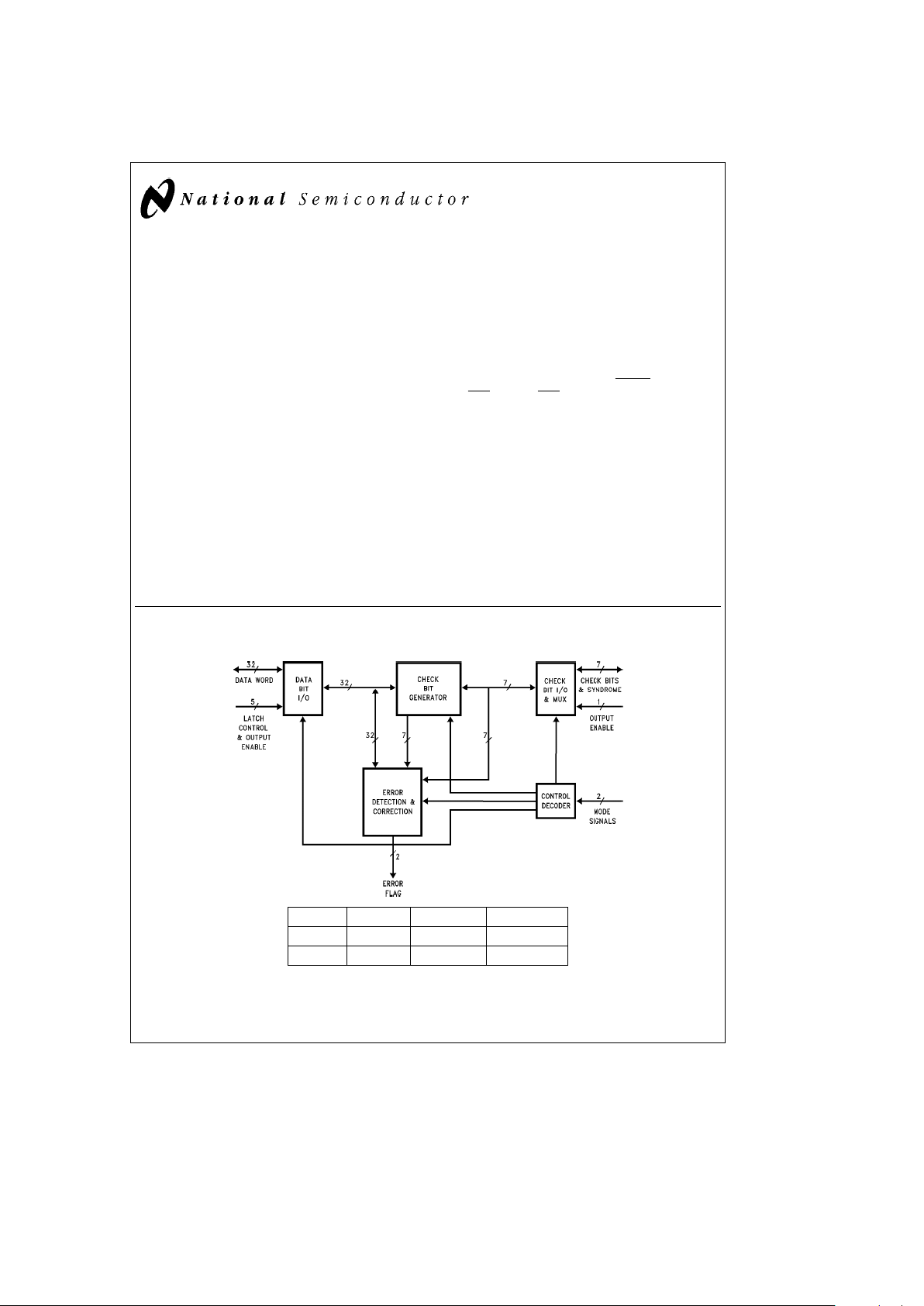
Simplified Functional Block
TL/F/9579– 9
Device Package Byte-Write Output
DP8406 52-Pin yes TRI-STATE
É
DP8406 68-Pin yes TRI-STATE
É
FASTÉand TRI-STATEÉare registered trademarks of National Semiconductor Corporation.
C
1995 National Semiconductor Corporation RRD-B30M105/Printed in U. S. A.
Page 2
Logic Symbol
TL/F/9579– 1
Unit Loading/Fan Out
54F/74F
Pin Names Description
U.L. Input I
IH/IIL
HIGH/LOW Output IOH/I
OL
CB0–CB6Check Word Bit, Input 3.5/1.083 70 mA/b650 mA
or TRI-STATE
É
Output 150/40 (33.3)b3 mA/24 mA (20 mA)
DB
0
–DB31Data Word Bit, Input 3.5/1.083 70 mA/b650 mA
or TRI-STATE Output 150/40 (33.3)
b
3 mA/24 mA (20 mA)
OEB0–OEB3Output Enable Data Bits 1.0/1.0 20 mA/b0.6 mA
LEDBO Output Latch Enable Data Bit 1.0/1.0 20 mA/b0.6 mA
OECB
Output Enable Check Bit 1.0/1.0 20 m A/b0.6 mA
S
0,S1
Select Pins 1.0/1.0 20 mA/b0.6 mA
ERR
Single Error Flag 50/33.3
b
1 mA/20 mA
MERR
Multiple Error Flag 50/33.3
b
1 mA/20 mA
Connection Diagrams
Pin Assignment
for LCC and PCC
52-Pin
TL/F/9579– 3
Order Number DP8406QV (74F632QC)
See NS Package Number V52A
Pin Assignment
for LCC and PCC
68-Pin
TL/F/9579– 8
NCÐNo internal connection
Order Number DP8406V (74F632VC)
See NS Package Number V68A
2
Page 3
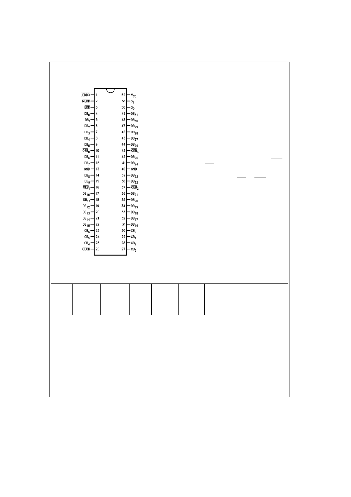
Connection Diagram (Continued)
Pin Assignment for
Side Brazed DIP
TL/F/9579– 2
Order Number DP8406D (74F632DC)
See NS Package Number D52A
Functional Description
MEMORY WRITE CYCLE DETAILS
During a memory write cycle, the check bits (CB0through
CB
6
) are generated internally in the EDAC by seven 16-input parity generators using the 32-bit data word as defined
in Table II. These seven check bits are stored in memory
along with the original 32-bit data word. This 32-bit word will
later be used in the memory read cycle for error detection
and correction.
ERROR DETECTION AND CORRECTION DETAILS
During a memory read cycle, the 7-bit check word is retrieved along with the actual data. In order to be able to
determine whether the data from memory is acceptable to
use as presented to the bus, the error flags must be tested
to determine if they are at the HIGH level.
The first case in Table III represents the normal, no-error
conditions. The EDAC presents HIGHs on both flags. The
next two cases of single-bit errors give a HIGH on MERR
and a LOW on ERR, which is the signal for a correctable
error, and the EDAC should be sent through the correction
cycle. The last three cases of double-bit errors will cause
the EDAC to signal LOWs on both ERR
and MERR, which is
the interrupt indication for the CPU.
Error detection is accomplished as the 7-bit check word and
the 32-bit data word from memory are applied to internal
parity generators/checkers. If the parity of all seven groupings of data and check bits is correct, it is assumed that no
error has occurred and both error flags will be HIGH.
TABLE I. Write Control Function
Memory EDAC Control DB Control
DB Output CB
Error Flags
Cycle Function S
1
S
0
Data I/O
OEB
n
Latch Check I/O Control
ERR
MERR
LEDBO OECB
Write
Generate
L L Input H X
Output
LHH
Check Word Check Bit*
*See Table II for details of check bit generation.
3
Page 4
Functional Description (Continued)
TABLE II. Parity Algorithm
Check Word
32-Bit Data Word
Bit
31 30 29 28 27 26 25 24 23 22 21 20 19 18 17 16 15 14 13 12 11 10 9 8 7 6 5 4 3 2 1 0
CB
0
XXXX XXXX X XXXXXX X
CB
1
XXXXXXXX XXXXXXXX
CB
2
XXXXXXXXXXXXXXXX
CB
3
XXX XXX XX XXX XXX XX
CB
4
XX XXXXXX XX XXXXXX
CB
5
XXXXXXXX XXXXXXXX
CB
6
XXXXXXXX XXXXXXXX
The seven check bits are parity bits derived from the matrix of data bits as indicated by X for each bit.
TABLE III. Error Function
Total Number of Errors Error Flags
Data Correction
32-Bit Data Word 7-Bit Check Word ERR MERR
0 0 H H Not Applicable
1 0 L H Correction
0 1 L H Correction
1 1 L L Interrupt
2 0 L L Interrupt
0 2 L L Interrupt
HeHIGH Voltage Level
L
e
LOW Voltage Level
If the parity of one or more of the check groups is incorrect,
an error has occurred and the proper error flag or flags will
be set LOW. Any single error in the 32-bit data word will
change the state of either three or five bits of the 7-bit
check word. Any single error in the 7-bit check word changes the state of only that one bit. In either case, the single
error flag (ERR
) will be set LOW while the dual error flag
(MERR
) will remain HIGH.
Any 2-bit error will change the state of an even number of
check bits. The 2-bit error is not correctable since the parity
tree can only identify single-bit errors. Both error flags are
set LOW when any 2-bit error is detected.
Three or more simultaneous bit errors can cause the EDAC
to believe that no error, a correctable error, or an uncorrectable error has occurred and will produce erroneous results
in all three cases. It should be noted that the gross-error
conditions of all LOWs and all HIGHs will be detected.
As the corrected word is made available on the data I/O
port (DB
0
through DB31), the check word I/O port (CB
0
through CB6) presents a 7-bit syndrome error code. This
syndrome error code can be used to locate the bad memory
chip. See Table V for syndrome decoding.
READ-MODIFY-WRITE (BYTE CONTROL) OPERATIONS
The ’F632 device is capable of byte-write operations. The
39-bit word from memory must first be latched into the Data
Bit and Check Bit input latches. This is easily accomplished
by switching from the read and flag mode (S
1
e
H, S
0
e
L)
to the latch input mode (S
1
e
H, S
0
e
H). The EDAC will
then make any corrections, if necessary, to the data word
and place it at the input of the output data latch. This data
word must then be latched into the output data latch by
taking LEDBO
from a LOW to a HIGH.
Byte control can now be employed on the data word
through the OEB
0
through OEB3controls. OEB0controls
DB
0
–DB7(byte 0), OEB1controls DB8–DB15(byte 1),
OEB
2
controls DB16–DB23(byte 2), and OEB3controls
DB
24
–DB31(byte 3). Placing a HIGH on the byte control will
disable the output and the user can modify the byte. If a
LOW is placed on the byte control, then the original byte is
allowed to pass onto the data bus unchanged. If the original
data word is altered through byte control, a new check word
must be generated before it is written back into memory.
This is easily accomplished by taking controls S
1
and S
0
LOW. Table VI lists the read-modify-write functions.
DIAGNOSTIC OPERATIONS
The ’F632 is capable of diagnostics that allow the user to
determine whether the EDAC or the memory is failing. The
diagnostic function tables will help the user to see the possibilities for diagnostic control. In the diagnostic mode
(S
1
e
L, S
0
e
H), the check word is latched into the input
latch while the data input latch remains transparent. This
lets the user apply various data words against a fixed known
check word. If the user applies a diagnostic data word with
an error in any bit location, the ERR
flag should be LOW. If a
diagnostic data word with two errors in any bit location is
applied, the MERR
flag should be LOW. After the check
word is latched into the input latch, it can be verified by
taking OECB
LOW. This outputs the latched check word.
The diagnostic data word can be latched into the output
data latch and verified. By changing from the diagnostic
mode (S
1
e
L, S
0
e
H) to the correction mode (S
1
e
H, S
0
e
H), the user can verify that the EDAC will correct the
diagnostic data word. Also, the syndrome bits can be produced to verify that the EDAC pinpoints the error location.
Table VII lists the diagnostic functions.
4
Page 5
Functional Description (Continued)
TABLE IV. Read, Flag and Correct Function
Memory EDAC Control DB Control
DB Output CB
Error Flags
Cycle Function S
1S0
Data I/O
OEB
n
Latch Check I/O Control
ERR
MERR
LEDBO OECB
Read Read & Flag H L Input H X Input H Enabled (Note 1)
Read Latch Input Latched Latched
Data & Check H H Input H L Input H Enabled (Note 1)
Bits Data Check Word
Read Output Output Output
Corrected Data H H Corrected L X Syndrome L Enabled (Note 1)
& Syndrome Bits Data Word Bits (Note 2)
Note 1: See Table III for error description.
Note 2: See Table V for error location.
TABLE V. Syndrome Decoding
Syndrome Bits
Error
6543210
LLLLLLL unc
L L L L L L H 2-Bit
L L L L L H L 2-Bit
LLLLLHH unc
L L L L H L L 2-Bit
LLLLHLH unc
LLLLHHL unc
L L L L H H H 2-Bit (Note 2)
L L L H L L L 2-Bit
LLLHLLH unc
LLLHLHL DB
31
L L L H L H H 2-Bit
LLLHHLL unc
L L L H H L H 2-Bit
L L L H H H L 2-Bit
LLLHHHH DB
30
L L H L L L L 2-Bit
LLHLLLH unc
LLHLLHL DB
29
L L H L L H H 2-Bit
LLHLHLL DB
28
L L H L H L H 2-Bit
L L H L H H L 2-Bit
L LH L HHH DB
27
LLHHLLL DB
26
L L H H L L H 2-Bit
L L H H L H L 2-Bit
LLHHLHH DB
25
L L H H H L L 2-Bit
LLHHHLH DB
24
L L H H H H L unc
L L H H H H H 2-Bit
Syndrome Bits
Error
6543210
L H L L L L L 2-Bit
LHLLL LHunc
LHLLLHLDB
7
L H L L L H H 2-Bit
LHLLHLLDB
6
L H L L H L H 2-Bit
L H L L H H L 2-Bit
LHLLHHHDB
5
LHLHLLLDB
4
L H L H L L H 2-Bit
L H L H L H L 2-Bit
LHLHLHHDB
3
L H L H H L L 2-Bit
LHLHHLHDB
2
L H L H H H L unc
L H L H H H H 2-Bit
LHHLL LLDB
0
L H H L L L H 2-Bit
L H H L L H L 2-Bit
L H H L L H H unc
L H H L H L L 2-Bit
LHHLHLHDB
1
LHHLHHLunc
L H H L H H H 2-Bit
L H H H L L L 2-Bit
L H H H L L H unc
L H H H L H L unc
L H H H L H H 2-Bit
LHHHHL Lunc
L H H H H L H 2-bit
L H H H H H L 2-bit
LHHHHHHCB
6
CB
X
e
Error in check bit X
DB
Y
e
Error in data bit Y
2-Bit
e
Double-bit error
unc
e
Uncorrectable multi-bit error
Note: 2-bit and unc condition will cause both ERR
and MERR to be LOW
Note 1: Syndrome bits for all LOWs. MERR
and ERR LOW for all LOWs,
only ERR
LOW for DB30error.
Note 2: Syndrome bits for all HIGHs.
5
Page 6

Functional Description (Continued)
TABLE V. Syndrome Decoding (Continued)
Syndrome Bits
Error
6543210
H L L L L L L 2-Bit
HLL L LLHunc
HLL L LHLunc
H L L L L H H 2-Bit
H L L L H L L unc
H L L L H L H 2-Bit
H L L L H H L 2-Bit
H L L L H H H unc
HLLHLLLunc
H L L H L L H 2-Bit
H L L H L H L 2-Bit
HLLHLHHDB
15
H L L H H L L 2-Bit
H L L H H L H unc
HLLHHHLDB
14
H L L H H H H 2-Bit
H L H L L L L unc
H L H L L L H 2-Bit
H L H L L H L 2-Bit
HLHL LHHDB
13
H L H L H L L 2-Bit
HLHLHLHDB
12
HLHLHHLDB
11
H L H L H H H 2-Bit
H L H H L L L 2-Bit
HLHHLLHDB
10
HLHHLHLDB
9
H L H H L H H 2-Bit
HLHHHL LDB
8
H L H H H L H 2-Bit
H L H H H H L 2-Bit
HLHHHHHCB
5
Syndrome Bits
Error
6543210
H H L L L L L unc
H H L L L L H 2-Bit
H H L L L H L 2-Bit
HHL L L HH DB
23
H H L L H L L 2-Bit
HHL L HL H DB
22
HHL L HHL DB
21
H H L L H H H 2-Bit
H H L H L L L 2-Bit
HHL H L LH DB
20
HHL H LHL DB
19
H H L H L H H 2-Bit
HHL HH L L DB
18
H H L H H L H 2-Bit
H H L H H H L 2-Bit
HHL HHHH CB
4
H H H L L L L 2-Bit
HHHL L LH DB
16
H H H L L H L unc
H H H L L H H 2-Bit
HHHLH L L DB
17
H H H L H L H 2-Bit
H H H L H H L 2-Bit
HHHLHHH CB
3
H H H H L L L unc (Note 1)
H H H H L L H 2-Bit
H H H H L H L 2-Bit
HHHH LHH CB
2
H H H H H L L 2-Bit
HHHHH LH CB
1
HHHHHH L CB
0
H H H H H H H None
CB
X
e
Error in check bit X
DB
Y
e
Error in data bit Y
2-Bit
e
Double-bit error
unc
e
Uncorrectable multi-bit error
Note: 2-bit and unc condition will cause both ERR
and MERR to be LOW
Note 1: Syndrome bits for all LOWs. MERR
and ERR LOW for all LOWs,
only ERR
LOW for DB30error.
Note 2: Syndrome bits for all HIGHs.
6
Page 7

Functional Description (Continued)
TABLE VI. Read-Modify-Write Function
Memory EDAC Control
DB Output CB
Error Flags
Cycle Function S
1
S
0
BYTEn* OEBn* Latch Check I/O Control
ERR
MERR
LEDBO OECB
Read Read & Flag H L Input H X Input H Enabled
Read Latch Input Latched Latched
Data & H H Input H L Input H Enabled
Check Bits Data Check Word
Read Latch Corrected
Latched
High Z H
Data Word into
HH
Output
HH
Output
L
Enabled
Output Latch
Data
Syndrome
Word
Bits
Modify/ Modify Input
Write Appropriate Modified H
Byte or Bytes
LL
BYTE
0
H
Output
LHH
& Generate New
Output
Check Word
Check Word
Unchanged L
BYTE
0
*OEB0controls DB0–DB7(BYTE0); OEB1controls DB8–DB15(BYTE1); OEB2controls DB16–DB23(BYTE2); OEB3controls DB24–DB31(BYTE3).
TABLE VII. Diagnostic Function
EDAC Control
DB Byte DB Output CB
Error Flags
Function S
1
S
0
Data I/O Control Latch Check I/O Control
ERR
MERR
OEB
n
LEDBO OECB
Read & Flag
HL
Input Correct
HX
Input Correct
HH
Data Word Check Bits
Latch Input Check
Word while Data Input Latched
Input Latch L H Diagnostic H L Input H Enabled
Remains Data Word* Check Bits
Transparent
Latch Diagnostic
Input
Output
Data Word into
L H Diagnostic H H
Latched L
Output Latch
Data Word*
Check Bits Enabled
High Z H
Latch Diagnostic
Latched
Output
Data Word into
HH
Input
HH
Syndrome L
Enabled
Input Latch
Diagnostic
Bits
Data Word
High Z H
Output Diagnostic
Output
Output
Data Word &
H H Diagnostic L H
Syndrome L
Enabled
Syndrome Bits
Data Word
Bits
High Z H
Output Corrected
Output
Output
Diagnostic Data
HH
Corrected
LL
Syndrome L
Enabled
Word & Output
Diagnostic
Bits
Syndrome Bits
Data Word
High Z H
*Diagnostic data is a data word with an error in one bit location except when testing the MERR error flag. In this case,the diagnostic data word will contain errors in
two bit locations.
7
Page 8

Block Diagram
TL/F/9579– 4
Timing Waveforms
Read, Flag and Correct Mode
TL/F/9579– 5
8
Page 9

Timing Waveforms (Continued)
Read, Correct and Modify Mode
TL/F/9579– 6
Diagnostic Mode
TL/F/9579– 7
9
Page 10

Absolute Maximum Ratings (Note 1)
If Military/Aerospace specified devices are required,
please contact the National Semiconductor Sales
Office/Distributors for availability and specifications.
Storage Temperature
b
65§Ctoa150§C
Ambient Temperature under Bias
b
55§Ctoa125§C
Junction Temperature under Bias
b
55§Ctoa175§C
VCCPin Potential to
Ground Pin
b
0.5V toa7.0V
Input Voltage (Note 2)
b
0.5V toa7.0V
Input Current (Note 2)
b
30 mA toa5.0 mA
Voltage Applied to Output
in HIGH State (with V
CC
e
0V)
Standard Output
b
0.5V to V
CC
TRI-STATE Output
b
0.5V toa5.5V
Current Applied to Output
in LOW State (Max) twice the rated I
OL
(mA)
ESD Last Passing Voltage (Min) 4000V
Note 1: Absolute maximum ratings are values beyond which the device may
be damaged or have its useful life impaired. Functional operation under
these conditions is not implied.
Note 2: Either voltage limit or current limit is sufficient to protect inputs.
Recommended Operating
Conditions
Free Air Ambient Temperature
Military
b
55§Ctoa125§C
Commercial 0
§
Ctoa70§C
Supply Voltage
Military
a
4.5V toa5.5V
Commercial
a
4.5V toa5.5V
DC Electrical Characteristics
Symbol Parameter
54F/74F
Units V
CC
Conditions
Min Typ Max
V
IH
Input HIGH Voltage 2.0 V Recognized as a HIGH Signal
V
IL
Input LOW Voltage 0.8 V Recognized as a LOW Signal
V
CD
Input Clamp Diode Voltage
b
1.2 V Min I
IN
eb
18 mA
V
OH
Output HIGH 54F 10% VCC2.5 I
OH
eb
1 mA (ERR, MERR,DBn,CBn)
Voltage 54F 10% V
CC
2.4 I
OH
eb
3mA(DBn,CBn)
74F 10% V
CC
2.5
V Min
I
OH
eb
1 mA (ERR, MERR,DBn,CBn)
74F 10% V
CC
2.4 I
OH
eb
3mA(DBn,CBn)
74F 5% V
CC
2.7 I
OH
eb
1 mA (ERR, MERR,DBn,CBn)
74F 5% V
CC
2.7 I
OH
eb
3mA(DBn,CBn)
V
OL
Output LOW 54F 10% V
CC
0.5 I
OL
e
20 mA (ERR, MERR,DBn,CBn)
Voltage 74F 10% V
CC
0.5 V Min I
OL
e
20 mA (ERR, MERR)
74F 10% V
CC
0.5 I
OL
e
24 mA (DBn,CBn)
I
IH
Input HIGH 54F 20.0
mA Max
V
IN
e
2.7V (S0,S1, OEBn, OECB, LEDBO)
Current 74F 5.0
I
BVI
Input HIGH Current 54F 100
mA Max
V
IN
e
7.0V (S0,S1, OEBn, OECB, LEDBO)
Breakdown Test 74F 7.0
I
BVIT
Input HIGH Current 54F 1.0
mA Max
V
IN
e
5.5V (CBn,DBn)
Breakdown (I/O) 74F 0.5
I
CEX
Output HIGH 54F 250
mA Max
V
OUT
e
V
CC
Leakage Current 74F 50
V
ID
Input Leakage
74F 4.75 V 0.0
I
ID
e
1.9 mA
Test All Other Pins Grounded
I
OD
Output Leakage
74F 3.75 mA 0.0
V
IOD
e
150 mV
Circuit Current All Other Pins Grounded
I
IL
Input LOW Current
b
0.6 mA Max V
IN
e
0.5V (S0,S1, OEB
n
, OECB, LEDBO)
I
IH
a
I
OZH
Output Leakage Current 70 mA Max V
I/O
e
2.7V (CBn,DBn)
I
IL
a
I
OZL
Output Leakage Current
b
650 mA Max V
I/O
e
0.5V (CBn,DBn)
I
OZH
Output Leakage Current 70 mA Max V
I/O
e
2.7V (CBn,DBn)
I
OZL
Output Leakage Current
b
650 mA Max V
I/O
e
0.5V (CBn,DBn)
I
OS
Output Short-Circuit Current
b
60
b
150 mA Max V
OUT
e
0V
I
ZZ
Bus Drainage Test 500 mA 0.0V V
OUT
e
5.25V (CBn,DBn)
I
CC
Power Supply Current 340 mA Max T
A
e
0§C–25§C
I
CC
Power Supply Current 325 mA Max T
A
e
25§C–70§C
10
Page 11

AC Electrical Characteristics
74F 54F 74F
T
A
ea
25§C
T
A,VCC
e
Mil TA,V
CC
e
Com
Symbol Parameter V
CC
ea
5.0V
C
L
e
50 pF C
L
e
50 pF
Units
C
L
e
50 pF
Min Typ Max Min Max Min Max
t
PLH
Propagation Delay 4.0 14.0 27.0 4.0 31.0
ns
t
PHL
DB or CB to ERR 4.0 10.5 18.0 4.0 20.0
t
PLH
Propagation Delay 4.0 21.0 27.0 4.0 31.0
ns
t
PHL
DB to ERR 4.0 14.0 18.0 4.0 20.0
t
PLH
Propagation Delay 5.0 17.0 27.0 5.0 31.0
ns
t
PHL
DB or CB to MERR 5.0 16.0 27.0 5.0 31.0
t
PLH
Propagation Delay 5.0 23.0 27.0 5.0 31.0
ns
t
PHL
DB to MERR 5.0 19.0 27.0 5.0 31.0
t
PLH
Propagation Delay 4.0 12.0 16.0 4.0 20.0
ns
t
PHL
S0and S1, LOW, to DB 4.0 12.0 16.0 4.0 20.0
t
PLH
Propagation Delay 4.0 10.5 14.0 4.0 15.0
ns
t
PHL
S1to CB 4.0 9.0 14.0 4.0 15.0
t
PLH
Propagation Delay
2.0 11.5 13.0 2.0 14.0 ns
S
0
or S1to ERR or MERR
t
PLH
Propagation Delay 4.0 16.0 23.0 4.0 25.0
ns
t
PHL
DB to CB 4.0 18.0 23.0 4.0 25.0
t
PLH
Propagation Delay 2.0 11.0 13.0 2.0 14.0
ns
t
PHL
LEDBO to DB 2.0 11.0 13.0 2.0 14.0
t
PZH
Output Enable Time 1.0 6.0 10.0 1.0 10.0
ns
t
PZL
OEBnto DB 1.0 6.0 10.0 1.0 10.0
t
PHZ
Output Disable Time 10 5.0 10.0 1.0 10.0
ns
t
PLZ
OEBnto DB 1.0 4.0 10.0 1.0 10.0
t
PZH
Output Enable Time 1.0 6.0 10.0 1.0 10.0
ns
t
PZL
OECB to CB 1.0 6.0 10.0 1.0 10.0
t
PHZ
Output Disable Time 1.0 5.0 10.0 1.0 10.0
ns
t
PLZ
OECB to CB 1.0 4.0 10.0 1.0 10.0
11
Page 12

AC Operating Requirements
74F 54F 74F
Symbol Parameter
T
A
ea
25§C
T
A,VCC
e
Mil TA,V
CC
e
Com Units
V
CC
ea
5.0V
Min Max Min Max Min Max
t
s
Setup Time, HIGH or LOW
3.0 3.0 ns
DB/CB before S
0
HIGH (S1HIGH)
ts(H) Setup Time, HIGH
12.0 14.0 ns
S0HIGH before LEDBO HIGH
ts(H) Setup Time, HIGH
00ns
LEDBO
HIGH before S0or S1LOW
ts(H) Setup Time, HIGH
00ns
LEDBO
HIGH before S1HIGH
t
s
Setup Time, HIGH or LOW
00ns
Diagnostic DB before S
1
HIGH
t
s
Setup Time, HIGH or LOW
Diagnostic CB before 3.0 3.0 ns
S
1
LOW or S0HIGH
t
s
Setup Time, HIGH or LOW
Diagnostic DB before 8.0 8.0 ns
LEDBO
HIGH (S1LOW, S0HIGH)
th(L) Hold Time, LOW
8.0 8.0 ns
S
0
LOW after S1HIGH
t
h
Hold Time, HIGH or LOW
8.0 8.0 ns
DB and CB Hold after S
0
HIGH
t
h
Hold Time, HIGH or LOW
8.0 8.0 ns
DB Hold after S
1
HIGH
t
h
Hold Time, HIGH or LOW
5.0 5.0 ns
CB Hold after S
1
LOW or S
0
HIGH
t
h
Hold Time, HIGH or LOW
Diagnostic DB after 0 0 ns
LEDBO HIGH (S1LOW, S0HIGH)
tw(L)* LEDBO Pulse Width 8.0 8.0 ns
t
corr
* Correction Time 25.0 28.0 ns
*Note: These parameters are guaranteed by characterization or other tests performed.
Ordering Information
The device number is used to form part of a simplified purchasing code where the package type and temperature range are
defined as follows:
74F 632 D C QR
Temperature Range Family Special Variations
74F
e
Commercial FAST QReCommercial grade device
54F
e
Military FAST with burn-in
QB
e
Military grade device with
Device Type
environmental and burn-in
processing
Package Code
DeCeramic DIP
Temperature Range
Q
e
52-Lead Plastic Chip Carrier (PCC)
C
e
Commercial (0§Ctoa70§C)
V
e
68-Lead Plastic Chip Carrier (PCC)
M
e
Military (b55§Ctoa125§C)
*Order DP8406QV, DP8406V or DP8406D
12
Page 13
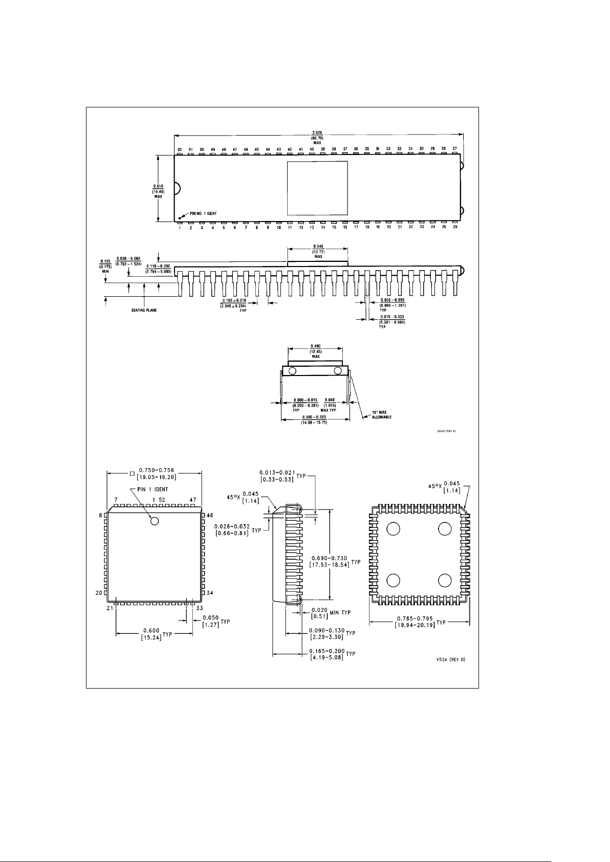
Physical Dimensions inches (millimeters)
52-Lead Side-Brazed Ceramic Dual-In-Line Package (D)
NS Package Number D52A
52-Lead Plastic Chip Carrier (Q)
NS Package Number V52A
13
Page 14

DP8406 (54F/74F632) 32-Bit Parallel Error Detection and Correction Circuit
Physical Dimensions inches (millimeters) (Continued)
68-Lead Plastic Chip Carrier (V)
NS Package Number V68A
LIFE SUPPORT POLICY
NATIONAL’S PRODUCTS ARE NOT AUTHORIZED FOR USE AS CRITICAL COMPONENTS IN LIFE SUPPORT
DEVICES OR SYSTEMS WITHOUT THE EXPRESS WRITTEN APPROVAL OF THE PRESIDENT OF NATIONAL
SEMICONDUCTOR CORPORATION. As used herein:
1. Life support devices or systems are devices or 2. A critical component is any component of a life
systems which, (a) are intended for surgical implant support device or system whose failure to perform can
into the body, or (b) support or sustain life, and whose be reasonably expected to cause the failure of the life
failure to perform, when properly used in accordance support device or system, or to affect its safety or
with instructions for use provided in the labeling, can effectiveness.
be reasonably expected to result in a significant injury
to the user.
National Semiconductor National Semiconductor National Semiconductor National Semiconductor
Corporation Europe Hong Kong Ltd. Japan Ltd.
1111 West Bardin Road Fax: (
a
49) 0-180-530 85 86 13th Floor, Straight Block, Tel: 81-043-299-2309
Arlington, TX 76017 Email: cnjwge@tevm2.nsc.com Ocean Centre, 5 Canton Rd. Fax: 81-043-299-2408
Tel: 1(800) 272-9959 Deutsch Tel: (
a
49) 0-180-530 85 85 Tsimshatsui, Kowloon
Fax: 1(800) 737-7018 English Tel: (
a
49) 0-180-532 78 32 Hong Kong
Fran3ais Tel: (
a
49) 0-180-532 93 58 Tel: (852) 2737-1600
Italiano Tel: (
a
49) 0-180-534 16 80 Fax: (852) 2736-9960
National does not assume any responsibility for use of any circuitry described, no circuit patent licenses are implied and National reserves the right at any time without notice to change said circuitry and specifications.
 Loading...