

Page 1
DP83959
8-Port Lite Ethernet Repeater Interface Controller
DP83959 8-Port Lite Ethernet Repeater Interface Controller
October 1997
General Description
The DP83959 8-Port Lite Ethernet Repeater Interface
Controller (LERIC8) is a single chip solution for unmanaged 10BASE-T Ethernet repeater (hub) products. By integrating electronics needed to support eight 10BASE-T
ports, a full level/drive compatible AUI port for a backbone
connection, and an internal power on reset circuit, a
LERIC8 based design requires only the addition of a few
passive components: crystal, transformers, connectors
and a power source.
The LERIC8 provides on-chip LED drivers that connect directly to LEDs via series resistors. In addition to the Link
OK, Port Partition, Global Activity and Global Collision LED
outputs, the LERIC8 provides an on chip network traffic
level monitor circuit with 8 LED outputs to drive a barg raph
type display.
The LERIC8 also provides an LED and Inter Repeater Bus
interface that is compatible with the DP83955/6 LERIC™
products.
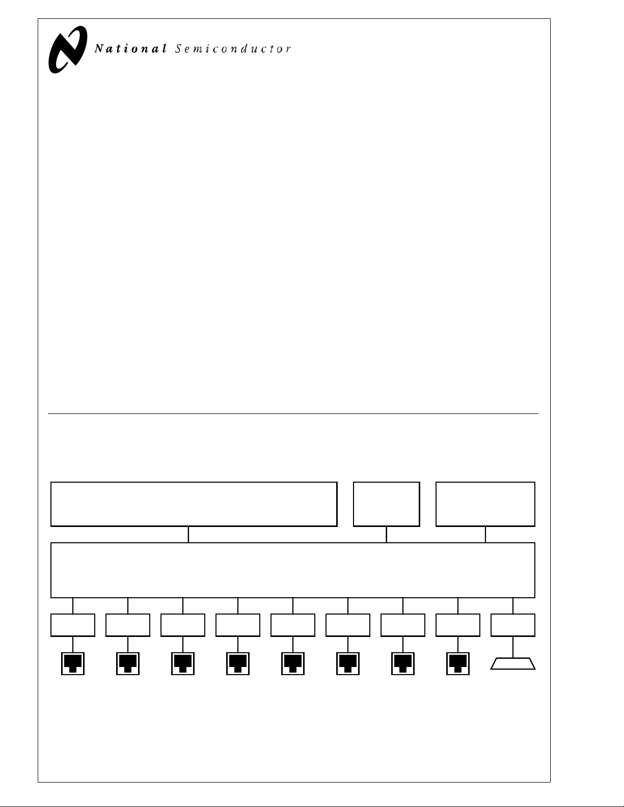
1.0 System Diagram
Features
■ Fully IEEE 802.3 Ethernet Repeater compliant
■ Eight IEEE 802.3 10BASE-T compliant ports with
on-chip transmit filters
■ One IEEE 802.3 compatible AUI port
■ Direct drive status LED outputs
■ Network traffic level monitor with direct drive LED
outputs
■ Automatic internal power-on reset function. External
TTL compatible reset pin provided for device testing if
required
■ Inter-LERIC™ bus for cascading up to 3 devices on a
single board
■ Register/LED status interface compatible with
DP83955/6 LERIC™ products
■ Single 20 MHz crystal or external 20 MHz oscillator
module operation
■ Single 5V supply
■ 160 pin PQFP package
Status LEDs (Optional)
Per 10BASE-T Port Link & Partition
AUI Port Partition
Global Activity, Global Collision
Network Traffic Bargraph
Alert (High Traffic or Long Partition)
DP83959 LERIC8
8-Port Lite Ethernet Repeater Interface Controller
Transformer
10BASE-T
Port 1
TRI-STATE® is a registered trademark of National Semiconductor Corporation.
™
and Inter-LERIC™ are trademarks of National Semiconductor Corporation.
LERIC
Transformer Transformer
10BASE-T
Port 2
10BASE-T
Port 3
10BASE-T
Port 4
TransformerTransformer TransformerTransformerTransformer
10BASE-T
Port 5
Transformer
10BASE-T
Port 6
20MHz
Oscillator
or Crystal
10BASE-T
Port 7
Inter Repeater Bus
(Optional)
10BASE-T
Port 8
AUI
Port
©1997 National Semiconductor Corporation
www.national.com
Page 2
2.0 Block Diagram
LEDs
Traffic
Bargraph
RXM
/TRAF2
/TRAF4
/TRAF1
/TRAF3
/TRAF5
/TRAF6
/TRAF7
/TRAF8
/ALERT
LEDs
Global
/GCOL
/GACT
X_IN
Clock
X_OUT
Reset
/ACKI
/MLOAD
RST_INT/EXT
/ACKO
IRD
Inter-
/IRE
Bus
LERIC
IRC
/COLN
/ACTN
RA[4:0]
/ANYXN
D[3:0]
/RD
/WR
Status
Config/
READY
Bus
/STR
DFS
BUFEN
DEF/OPT
Traffic
Monitor
Decoder
Manchester
RX
Mux
LED
Interface
Crystal
Oscillator
Reset
Generator
Bus
Interface
Inter-LERIC
and Timers
Repeater Main State Machine
Compatible
& DP83955/6
Configuration
Buffer
Elasticity
and
Encoder
TX De-Mux
Manchester
Interface
& Register
Status/LED
DP83959 LERIC8
AUI Port 0
AUI Interface
RX0+/-
Port State Machine
Port Partition Logic
Port Status Register/LED Driver
TX0+/-
CD0+/-
/PART0
AUI
Port 0
10BASE-T Port 1
with Waveshaping
Port State Machine
Twisted Pair Transceiver
RX1+/-
Port Partition Logic
TX1+/-
P/L_1A
Port 1
10BASE-T
10BASE-T Port 2
Port Status Register/LED Driver
P/L_1B
TX2+/-
RX2+/-
10BASE-T
P/L_2B
P/L_2A
Port 2
TX3+/-
RX3+/-
2
10BASE-T Port 3
TX4+/-
RX4+/-
P/L_3B
P/L_3A
Port 3
10BASE-T
10BASE-T Port 4
TX5+/-
RX5+/-
P/L_4B
P/L_4A
Port 4
10BASE-T
10BASE-T Port 5
TX6+/-
RX6+/-
P/L_5B
P/L_5A
Port 5
10BASE-T
10BASE-T Port 6
TX7+/-
RX7+/-
P/L_6B
P/L_6A
Port 6
10BASE-T
10BASE-T Port 7
TX8+/-
RX8+/-
P/L_7B
P/L_7A
Port 7
10BASE-T
10BASE-T Port 8
P/L_8B
P/L_8A
Port 8
10BASE-T
www.national.com
Page 3

Table of Contents
1.0 System Diagram . . . . . . . . . . . . . . . . . . . . . . . . . . . . . . . .1
2.0 Block Diagram . . . . . . . . . . . . . . . . . . . . . . . . . . . . . . . . . .2
3.0 Pin Connection Diagram . . . . . . . . . . . . . . . . . . . . . . . . .4
4.0 Pin Descriptions . . . . . . . . . . . . . . . . . . . . . . . . . . . . . . . .5
4.1 AUI Port (Port 0) . . . . . . . . . . . . . . . . . . . . . . . . . . .5
4.2 Twisted Pair Ports (Ports 1 - 8) . . . . . . . . . . . . . . . . 5
4.3 Status LED Interface . . . . . . . . . . . . . . . . . . . . . . . .7
4.4 Inter-LERIC Bus Interface . . . . . . . . . . . . . . . . . . . .9
4.5 Clock Interface . . . . . . . . . . . . . . . . . . . . . . . . . . . .10
4.6 Register/Configuration Interface . . . . . . . . . . . . . .11
4.7 Miscellaneous Pins . . . . . . . . . . . . . . . . . . . . . . . .12
4.8 Power and Ground Pins . . . . . . . . . . . . . . . . . . . . .13
5.0 Functional Description . . . . . . . . . . . . . . . . . . . . . . . . . . 14
5.1 Repeater Main State Machine & Timers . . . . . . . .14
5.2 Port State Machines . . . . . . . . . . . . . . . . . . . . . . . .14
5.3 Receive Multiplexer . . . . . . . . . . . . . . . . . . . . . . . .14
5.4 Manchester Decoder 1 . . . . . . . . . . . . . . . . . . . . . . .4
5.5 Elasticity Buffer . . . . . . . . . . . . . . . . . . . . . . . . . . .14
5.6 Transmit DE-Multiplexer & Manchester Encoder . . 15
5.7 Inter-LERIC Bus Interface . . . . . . . . . . . . . . . . . . .15
5.8 Clock Interface . . . . . . . . . . . . . . . . . . . . . . . . . . . .15
5.9 Reset Interface . . . . . . . . . . . . . . . . . . . . . . . . . . . .15
5.10 Traffic Monitor LED Interface . . . . . . . . . . . . . . . . .16
5.11 Port Status LEDs . . . . . . . . . . . . . . . . . . . . . . . . . .18
5.12 Configuration/Register Interface . . . . . . . . . . . . . .18
5.13 Min/Max Mode LED Interface . . . . . . . . . . . . . . . .19
5.14 AUI Port 0 . . . . . . . . . . . . . . . . . . . . . . . . . . . . . . .19
5.15 10BASE-T Ports 1-8 . . . . . . . . . . . . . . . . . . . . . . .19
6.0 LERIC8 Registers 22
6.1 Register Address Map . . . . . . . . . . . . . . . . . . . . . 22
6.2 LERIC8 Status Register . . . . . . . . . . . . . . . . . . . . 23
6.3 Port 0 (AUI) Status/Configuration Register . . . . . . 24
6.4 Ports 1-8 (10BASE-T) Status/Configuration
Registers . . . . . . . . . . . . . . . . . . . . . . . . . . . . . . . 25
7.0 System Considerations . . . . . . . . . . . . . . . . . . . . . . . . 26
7.1 Cascading . . . . . . . . . . . . . . . . . . . . . . . . . . . . . . . 26
7.2 IEEE Conformance . . . . . . . . . . . . . . . . . . . . . . . . 26
8.0 DC Specifications . . . . . . . . . . . . . . . . . . . . . . . . . . . . . 27
9.0 Switching Characteristics . . . . . . . . . . . . . . . . . . . . . . 28
9.1 Port Arbitration . . . . . . . . . . . . . . . . . . . . . . . . . . . 28
9.2 Receive - AUI Port . . . . . . . . . . . . . . . . . . . . . . . . 28
9.3 Receive - 10BASE-T Ports . . . . . . . . . . . . . . . . . . 29
9.4 Transmit - AUI Port . . . . . . . . . . . . . . . . . . . . . . . . 29
9.5 Transmit - 10BASE-T Ports . . . . . . . . . . . . . . . . . 30
9.6 Collision - AUI Port . . . . . . . . . . . . . . . . . . . . . . . . 30
9.7 Collision - 10BASE-T Ports . . . . . . . . . . . . . . . . . 31
9.8 Collision - All Ports - Inter-LERIC Bus . . . . . . . . . 32
9.9 Collision - All Ports - One Port Left . . . . . . . . . . . . 32
9.10 Reset . . . . . . . . . . . . . . . . . . . . . . . . . . . . . . . . . . 33
9.11 LED Strobe . . . . . . . . . . . . . . . . . . . . . . . . . . . . . . 33
9.12 Register Read . . . . . . . . . . . . . . . . . . . . . . . . . . . . 34
9.13 Register Write . . . . . . . . . . . . . . . . . . . . . . . . . . . . 35
9.14 Inter-LERIC Bus (Packet Output) . . . . . . . . . . . . . 36
9.15 Inter-LERIC Bus (Packet Input) . . . . . . . . . . . . . . 36
10.0 AC Timing Test Conditions . . . . . . . . . . . . . . . . . . . . . 37
10.1 General Test Conditions . . . . . . . . . . . . . . . . . . . . 37
10.2 Capacitance. . . . . . . . . . . . . . . . . . . . . . . . . . . . . . 37
11.0 Physical Dimensions . . . . . . . . . . . . . . . . . . . . . . . . . . 38
3
www.national.com
Page 4
3.0 Pin Connection Diagram
NC
TX3+
TX3GND_P3
VCC_P3
RX3+
RX3-
RX2+
RX2VCC_P2
GND_P2
TX2+
TX2-
TX1+
TX1GND_P1
VCC_P1
RX1+
RX1-
GND_OSC
VCC_OSC
/MLOAD_
RST_INT/EXT
X_IN
X_OUT
VCC
GND
GND_LED
/ALERT
/TRAF1
/TRAF2
/TRAF3
GND_LED
/TRAF4
/TRAF5
/TRAF6
GND_LED
/TRAF7
/TRAF8
NC
121
122
123
124
125
126
127
128
129
130
131
132
133
134
135
136
137
138
139
140
141
142
143
144
145
146
147
148
149
150
151
152
153
154
155
156
157
158
159
160
NC
120
1
119
2
NC
TX4-
118
3
TX4+
117
4
116
5
VCC_P4
RX4-
GND_P4
115
114
7
6
RX4+
TEST_EN
113
112
8
9
TEST_4
RTX
GND_ANLG
VCC
VCC_ANLG
GND
REQ
TEST_3
109
105
108
107
106
104
111
110
DP83959VUL
LERIC8
160 pin PQFP
11
15
12
16
13
10
17
14
TEST_2
TEST_5
FIL_TTL
RX5-
101
100
103
102
Top View
19
20
21
18
RX5+
VCC_P5
98
99
22
23
TX5+
GND_P5
TX5-
97
96
95
26
24
25
TX6-
94
27
TX6+
GND_P6
93
92
28
29
VCC_P6
RX6-
RX6+
90
89
91
30
31
32
RX7-
88
33
RX7+
VCC_P7
86
87
34
35
TX7+
GND_P7
TX7-
85
84
83
38
36
37
NC
NC
82
81
80
NC
TX8-
79
78
TX8+
77
GND_P8
VCC_P8
76
RX8-
75
74
RX8+
73
RX0RX0+
72
CD0-
71
70
CD0+
69
TX0TX0+
68
VCC_AUI
67
66
GND_AUI
65
GND_PLL
VCC_PLL
64
RA4
63
62
RA3
61
RA2
RA1
60
RA0
59
58
VCC
57
GND
D3
56
D2
55
54
D1
53
D0
BUFEN
52
READY
51
50
/COLN
49
/ANYXN
/ACTN
48
GND
47
46
VCC
45
IRD
/IRE
44
IRC
43
42
NC
41
NC
39
40
NC
NC
GND
/GACT
/GCOL
P/L_1A
VCC_LED
P/L_1B
P/L_2A
P/L_2B
GND_LED
P/L_3A
P/L_4A
VCC_LED
GND_LED
P/L_5A
P/L_5B
P/L_6A
P/L_7A
VCC_LED
P/L_6B
P/L_4B
P/L_3B
Order Number DP83959VUL
See NS Package Number VUL160A
P/L_7B
P/L_8A
GND_LED
P/L_8B
TEST_1
/RD
/WR
DEF/OPT
/ACKI
/ACKO
VCC
GND
/STR
DFS
RXM
NC
/PART0
4
www.national.com
Page 5
4.0 Pin Descriptions
Key to Pin Type:
O = TTL Compatible Output I/O = TTL Compatible Input/Output
O (ECL) = ECL Compatible Output I/O (O.D.) = TTL Compatible Input/Open Drain Output
I = TTL Compatible Input TPO = Twisted Pair Interface Compatable Output
I (ECL) = ECL Compatible Input TPI = Twisted Pair Interface Compatable Input
OZ = TTL Compatible TRI-STATE
O (O.D.) = Open Drain Output
4.1 AUI PORT (PORT 0)
Signal Name Type Pin # Description
®
Output AI = Analog Input
TX0+ O
(ECL)
TX0- O
(ECL)
RX0+ I
(ECL)
RX0- I
(ECL)
CD0+ I
(ECL)
CD0- I
(ECL)
68 AUI Transmit +: The AUI transmit path includes National Semiconductor's
patented low power dissipation differential drivers that do not need external load
resistors. This output should be connected directly to the AUI isolation tr ansformer.
69 AUI T ransmit -: The AUI transmit path includes National Semiconductor's patented
low power dissipation differential drivers that do not need external load resistors.
This output should be connected directly to the AUI isolation transformer.
72 AUI Receive +: This input should be terminated with 39Ω to GND via a series DC
blocking capacitor (shared with RX0-). Refer to Figure8.
73 AUI Receive -: This input should be terminated with 39Ω to GND via a ser ies DC
blocking capacitor (shared with RX0+). Refer to Figure8.
70 AUI Collision Detect +: This input should be terminated with 39Ω to GND via a
series DC blocking capacitor (shared with CD0-). Refer to Figure 8.
71 AUI Collision Detect -: This input should be terminated with 39Ω to GND via a
series DC blocking capacitor (shared with CD0+). Refer to Figure 8.
4.2 TWISTED PAIR PORTS (PORTS 1 - 8)
Signal Name Type Pin # Description
REQ AI 108 Equalization Resistor: A resistor connected between this pin and GND or V
adjusts the equalization step amplitude on the 10BASE-T Manchester encoded
transmit data for all eight 10BASE-T ports. No resistor is required for operation with
cable length of up to 100 meters.
RTX AI 107 Extended Cable Resistor:A resistor connected between this pin and GND or V
adjusts the amplitude of the differential transmit outputs for all eight 10BASE-T
ports. No resistor is required for operation with cable length of up to 100 meters.
CC
CC
5
www.national.com
Page 6
4.0 Pin Descriptions (Continued)
The values of the resistor/capacitor parallel source impedance matching networks connected to each of the
10BASE-T transmit outputs will depend upon PCB layout
factors (such as track length, width, route etc.) and will hav e
to be determined for each design. Preliminary laboratory
Signal Name Type Pin # Description
TX1
+ TPO 134, 135 Port 1 Transmit: 10BASE-T transmitter output - requires a series source
impedance matching network consisting of a resistor and capacitor in parallel. The
values of these components will be application specific.
RX1
+ TPI 138, 139 Port 1 Receive: 10BASE-T receiver input - requires a 50Ω receive termination.
+ TPO 132, 133 Port 2 Transmit: 10BASE-T transmitter output - requires a series source
TX2
impedance matching network consisting of a resistor and capacitor in parallel. The
values of these components will be application specific.
RX2
+ TPI 128, 129 Port 2 Receive: 10BASE-T receiver input - requires a 50Ω receive termination.
+ TPO 122, 123 Port 3 Transmit: 10BASE-T transmitter output - requires a series source
TX3
impedance matching network consisting of a resistor and capacitor in parallel. The
values of these components will be application specific.
RX3
+ TPI 126, 127 Port 3 Receive: 10BASE-T receiver input - requires a 50Ω receive termination.
+ TPO 117, 118 Port 4 Transmit: 10BASE-T transmitter output - requires a series source
TX4
impedance matching network consisting of a resistor and capacitor in parallel. The
values of these components will be application specific.
RX4
+ TPI 113, 114 Port 4 Receive: 10BASE-T receiver input - requires a 50Ω receive termination.
+ TPO 95, 96
TX5
Port 5 Transmit: 10BASE-T transmitter output - requires a series source impedance matching network consisting of a resistor and capacitor in parallel. The values
of these components will be application specific.
work suggests that values of 13.5Ω and 820 pF are appropriate in order to meet IEEE 802.3 specifications and EMI
requirements - these values should be taken as a starting
point for investigation. Refer to Figure 9.
RX5
+ TPI 99, 100
TX6+ TPO 93, 94
RX6
+ TPI 89, 90
TX7+ TPO 83, 84
RX7
+ TPI 87, 88
TX8+ TPO 78, 79
RX8
+ TPI 74, 75
Port 5 Receive: 10BASE-T receiver input - requires a 50Ω receive termination.
Port 6 Transmit: 10BASE-T transmitter output - requires a series source imped-
ance matching network consisting of a resistor and capacitor in parallel. The values
of these components will be application specific.
Port 6 Receive: 10BASE-T receiver input - requires a 50Ω receive termination.
Port 7 Transmit: 10BASE-T transmitter output - requires a series source imped-
ance matching network consisting of a resistor and capacitor in parallel. The values
of these components will be application specific.
Port 7 Receive: 10BASE-T receiver input - requires a 50Ω receive termination.
Port 8 Transmit: 10BASE-T transmitter output - requires a series source imped-
ance matching network consisting of a resistor and capacitor in parallel. The values
of these components will be application specific.
Port 8 Receive: 10BASE-T receiver input - requires a 50Ω receive termination.
6
www.national.com
Page 7

4.0 Pin Descriptions (Continued)
4.3 STATUS LED INTERFACE
All the DP83959's direct drive LED outputs can drive up to
14mA maximum. The LED outputs are intended to drive an
external LED with a series current limiting resistor. The P artition/Link OK LED outputs can sink or source current and
are thus suitable for driving single or bi-color LEDs directly.
Bi-color LEDs can be connected between the A and B outputs (with series current limiting resistors) (see section
5.11).
The direct drive LED outputs are asserted during pow-
er-on/reset (either internal or external reset) and remain as-
Signal Name Type Pin # Description
P/L_1A
P/L_1B
P/L_2A
P/L_2B
O (14mA
max.)
O (14mA
max.)
6
9
10
11
Partition/Link OK LED 1 - A and B: LED outputs (for use with single or
bi-color LEDs) with the following function:
Link Status
/OK
/OK
OK
OK
Partition/Link OK LED 2 - A and B: LED outputs (for use with single or
bi-color LEDs) with the following function:
Link Status
/OK
/OK
OK
OK
serted for 1 second (nominal) following the trailing edge of
the internal/external reset signal. During the LED test at
power-on/reset, the Partition/Link OK 'A' outputs will all be
logic '1' and the 'B' outputs logic '0'.
DP83955/6 compatible LED drive outputs are only asserted
for the duration of the 1 second LED test following the trailing edge of the internal/external reset (they are not asserted
during reset). The DP83955/6 compatible status LED
scheme is described in the functional description
(Section 5.13) as it requires external circuitry to latch the
status and drive the LEDs.
Partition Status
/PART
PART
/PART
PART
Partition Status
/PART
PART
/PART
PART
A Output
1
1
0
1
A Output
1
1
0
1
B Output
1
1
1
0
B Output
1
1
1
0
P/L_3A
P/L_3B
P/L_4A
P/L_4B
P/L_5A
P/L_5B
O (14mA
max.)
O (14mA
max.)
O (14mA
max.)
12
13
14
17
18
19
Partition/Link OK LED 3 - A and B: LED outputs (for use with single or
bi-color LEDs) with the following function:
Link Status
/OK
/OK
OK
OK
Partition/Link OK LED 4 - A and B: LED outputs (for use with single or
bi-color LEDs) with the following function:
Link Status
/OK
/OK
OK
OK
Partition/Link OK LED 5 - A and B: LED outputs (for use with single or
bi-color LEDs) with the following function:
Link Status
/OK
/OK
OK
OK
Partition Status
/PART
PART
/PART
PART
Partition Status
/PART
PART
/PART
PART
Partition Status
/PART
PART
/PART
PART
A Output
1
1
0
1
A Output
1
1
0
1
A Output
1
1
0
1
B Output
1
1
1
0
B Output
1
1
1
0
B Output
1
1
1
0
7
www.national.com
Page 8

4.0 Pin Descriptions (Continued)
Signal Name Type Pin # Description
P/L_6A
P/L_6B
P/L_7A
P/L_7B
P/L_8A
P/L_8B
/TRAF1 O (14mA
/TRAF2 O (14mA
/TRAF3 O (14mA
/TRAF4 O (14mA
/TRAF5 O (14mA
/TRAF6 O (14mA
/TRAF7 O (14mA
/TRAF8 O (14mA
/ALERT O (14mA
O (14mA
max.)
O (14mA
max.)
O (14mA
max.)
max.)
max.)
max.)
max.)
max.)
max.)
max.)
max.)
max.)
20
21
22
25
26
27
150 Traffic Monitor LED 1 (1%):
151 Traffic Monitor LED 2 (2%):
152 Traffic Monitor LED 3 (3%):
154 Traffic Monitor LED 4 (6%):
155 Traffic Monitor LED 5 (12%):
156 Traffic Monitor LED 6 (25%):
158 Traffic Monitor LED 7 (50%):
159 Traffic Monitor LED 8 (>80%):
149 Alert LED: This LED output indicates that greater than 80% traffic level for
Partition/Link OK LED 6 - A and B: LED outputs (for use with single or
bi-color LEDs) with the following function:
Link Status
/OK
/OK
OK
OK
Partition/Link OK LED 7 - A and B: LED outputs (for use with single or
bi-color LEDs) with the following function:
Link Status
/OK
/OK
OK
OK
Partition/Link OK LED 8 - A and B: LED outputs (for use with single or
bi-color LEDs) with the following function:
Link Status
/OK
/OK
OK
OK
0 = 1% Traffic Level reached or exceeded
1 = Traffic Level less than 1%
0 = 2% Traffic Level reached or exceeded
1 = Traffic Level less than 2%
0 = 3% Traffic Level reached or exceeded
1 = Traffic Level less than 3%
0 = 6% Traffic Level reached or exceeded
1 = Traffic Level less than 6%
0 = 12% Traffic Level reached or exceeded
1 = Traffic Level less than 12%
0 = 25% Traffic Level reached or exceeded
1 = Traffic Level less than 25%
0 = 50% Traffic Level reached or exceeded
1 = Traffic Level less than 50%
0 = >80% Traffic Level reached or exceeded
1 = Traffic Level less than 80%
one second or more has occurred, or a 10BASE-T port partition has occurred.
The output remains active until the current event condition ceases or, if the
event condition is shorter than 30ms, for a minimum of 30ms (nominal value).
Active low.
Partition Status
/PART
PART
/PART
PART
Partition Status
/PART
PART
/PART
PART
Partition Status
/PART
PART
/PART
PART
A Output
1
1
0
1
A Output
1
1
0
1
A Output
1
1
0
1
B Output
1
1
1
0
B Output
1
1
1
0
B Output
1
1
1
0
8
www.national.com
Page 9
4.0 Pin Descriptions (Continued)
Signal Name Type Pin # Description
/PART0 O (14mA
39 Partition LED 0: Partition LED output for the AUI port. Active low.
max.)
/GCOL O (14mA
max.)
4 Global Collision LED: Global collision status LED output. Indicates collision
activity on any port. Active low. This output will be asserted low until the start
of the next network event or for a maximum of 30ms (nominal value).
/GACT O (14mA
max.)
5 Global Activity LED: Global Activity LED output. Indicates receive activity
(carrier sense active) on any port. Active low. This output will be asserted low
until the start of the next network event or for a maximum of 30ms (nominal
value).
4.4 INTER-LERIC BUS INTERFACE
Signal Name Type Pin # Description
/ACKI I 32 Acknowledge Input: to the network ports' arbitration chain. If the Inter-LERIC
bus is not being used or if this LERIC8 is at the top of the /ACKI - /A CKO chain
or is the only repeater chip in the system, this pin should be connected to V
either directly or via a pull-up resistor (≈ 4.7 kΩ). Otherwise, this input should
be driven from the previous LERIC8's /ACKO output.
/ACKO O 33 Acknowledge Output: from the network ports' arbitration chain, connected to
the /ACKI of the next repeater chip in the /ACKI - /ACKO chain. If this LERIC8
is not chained to any other repeater chips, this pin should be left unconnected.
IRD I/O 45 Inter-LERIC Data: When asser ted as an output this signal provides a serial
data stream in NRZ format. The signal is asserted by a LERIC8 when it is
receiving data from one of its network segments. The default condition of this
signal is to be an input. In this state it may be driven by other devices on the
Inter-LERIC bus. If the Inter-LERIC bus is not being used, this pin should be
left unconnected (it has an internal pull-up resistor of 14 kΩ) or pulled up to
V
via an external resistor.
CC
/IRE I/O 44 Inter-LERIC Enable: When asserted as an output this signal provides an
activity framing enable for the serial data stream. The signal is asserted by a
LERIC8 when it is receiving data from one of its network segments. The
default condition of this signal is to be an input. In this state it may be driven b y
other devices on the Inter-LERIC bus. If the Inter-LERIC bus is not being
used, this pin should be left unconnected (it has an internal pull-up resistor of
14 kΩ) or pulled up to V
be used, this signal should have an external 680Ω pull-up resistor to ensure
fast de-assertion.
IRC I/O 43 Inter-LERIC Clock: When asserted as an output this signal provides a clock
signal for the serial data stream. Data (IRD) is changed on the falling edge of
the clock. The signal is asserted by a LERIC8 when it is receiving data from
one of its network segments. The default condition of this signal is to be an
input. When an input, IRD is sampled on the rising edge of the clock. In this
state it may be driven by other devices on the Inter-LERIC bus. If the
Inter-LERIC bus is not being used, this pin should be left unconnected (it has
an internal pull-up resistor of 14 kΩ) or pulled up to V
resistor.
/COLN I/O 50 Collision on Port N: This denotes that a collision is occurring on the port
receiving the data packet (Port N). The default condition of this signal is to be
an input. In this state it may be driven by other devices on the Inter-LERIC
bus. If the Inter-LERIC bus is not being used, this pin should be left
unconnected (it has an internal pull-up resistor of 3.5 kΩ) or pulled up to V
via an external resistor. If the Inter-LERIC bus is to be used, this signal should
have an external 680Ω pull-up resistor to ensure fast de-assertion.
via an external resistor. If the Inter-LERIC b us is to
CC
via an external
CC
CC
CC
9
www.national.com
Page 10
4.0 Pin Descriptions (Continued)
Signal Name Type Pin # Description
/ACTN I/O (O.D.) 48 Activity on Port N: The LERIC8 asser ts this signal when data or collision
information is received from one of its network segments. The LERIC8 senses
this signal when this or another LERIC8 in a multi-LERIC system is receiving
data or collision information. If the Inter-LERIC bus is not being used, this pin
should be left unconnected (it has an internal pull-up resistor of 3.5 kΩ) or
pulled up to V
this signal should have an external 680Ω pull-up resistor to ensure fast
de-assertion.
/ANYXN I/O (O.D.) 49 Activity on Any Port Except Port N: The LERIC8 asserts this signal when a
transmit collision is experienced or multiple ports have active collisions on
their network segments. The LERIC8 senses this signal when this or another
LERIC8 in a multi-LERIC system is experiencing transmit collisions or multiple
ports have active collisions on their network segments. If the Inter-LERIC bus
is not being used, this pin should be left unconnected (it has an internal
pull-up resistor of 14 kΩ) or pulled up to V
Inter-LERIC bus is to be used, this signal should have an external 680Ω
pull-up resistor to ensure fast de-assertion.
4.5 CLOCK INTERFACE
Signal Name Type Pin # Description
X_IN I 144 20 MHz Crystal Oscillator Input: This pin can be used to connect an
external 20MHz crystal (between X_IN and X_OUT) as shown in Figure 2, or
as an external TTL compatible 20MHz oscillator module input as shown in
Figure 3.
X_OUT O 145 20 MHz Crystal Oscillator Output: This pin is used to connect to an external
20 MHz crystal (between X_IN and X_OUT) as shown in Figure 2. When
using an external 20 MHz crystal oscillator module connected to the X_IN
input, this pin should be left unconnected as shown in Figure 3.
via an external resistor. If the Inter-LERIC bus is to be used,
CC
via an external resistor. If the
CC
10
www.national.com
Page 11

4.0 Pin Descriptions (Continued)
4.6 REGISTER/CONFIGURATION INTERFACE
Signal Name Type Pin # Description
RA4
RA3
RA2
RA1
RA0
D3
D2
D1
D0
/RD I 31 Read Strobe: When strobed low, this input schedules a register read access
/WR I 30 Write Strobe: When strobed low, this input schedules a register write access
/READY O 51 Ready Handshake: The falling edge of this active low signal during a read
/STR O 36 Display Update Str obe:When using the DP83955/6 compatible status LEDs,
DFS O 37 Display Frozen Strobe: Asserted high when the display data for each pac k et
BUFEN O 52 Buffer Enable: Used to control an external buffer (if required) for the data
/MLOAD I 142 Mode Load/Reset: TTL level reset input (not Schmitt) for external reset or
I/O 63
62
61
60
59
I/O 56
55
54
53
Register Address [4:0]: Address input value for the current register access.
These pins also provide DP83955/6 compatible LED status: during display
update cycles these pins become outputs that provide port address and data
for LED display purposes. Pins RA[1:4] cycle values from 0h to 9h while RA0
provides Bad Polarity status for the 10BASE-T ports. See Section 5.13 for
more details. If the DP83955/6 compatible LEDs and register interface are not
being used, these pins should be left unconnected.
In Option mode (see DEF/OPT), the logic levels present on RA[4:0] at reset
(set by pull-up or pull-down resistors) are latched into the configuration
registers. See section 5.12 for more information.
Data [3:0]: Bi-directional register data. /RD and /WR control the data
direction. With /RD low and /WR high, D[3:0] are outputs and with /RD high
and /WR low, D[3:0] are inputs. These pins also provide the DP83955/6
compatible status outputs for latching to LEDs. See Section 5.13 for more
details. If the DP83955/6 compatible LEDs and register interface are not being
used, these pins should be left unconnected.
In Option mode (see DEF/OPT), the logic levels present on D[3:0] at reset (set
by pull-up or pull-down resistors) are latched into the configuration registers.
See Section 5.12 for more information.
to the register addressed by the RA[4:0] pins. If the register interface is not
being used, this pin should be connected to V
resistor (≈4.7 kΩ).
to the register addressed by the RA[4:0] pins. If the register interface is not
being used, this pin should be connected to V
resistor (≈4.7 kΩ).
cycle indicates that data is stable and valid for sampling. In write cycles, the
falling edge of /READY denotes that the write data has been latched by the
LeRIC8. Therefore, data must have been available and stable for this
operation to be successful.
this active low signal controls the latching of display data f or network ports into
the external display latches. If not required, this pin should be left
unconnected.
is frozen at the end of the repeater transmission of the packet until the start of
the next network event or for a maximum of 30ms (nominal value). This
ensures DP83955/6 compatible status LEDs are visible even for single
network events.
bus, D[3:0]. Extermal buffer will be necessary in systems having a register
interface.
test purposes. If not required, this pin should be connected to V
directly or via a pull-up resistor (≈4.7 kΩ). On the rising (trailing) edge of
/MLOAD, the logic levels present on the D[3:0] and RA[4:0] inputs (set by
pull-up or pull-down resistors) are latched into the configuration registers.
either directly or via a pull-up
CC
either directly or via a pull-up
CC
CC
either
11
www.national.com
Page 12
4.0 Pin Descriptions (Continued)
Signal Name Type Pin # Description
RST_INT/EXT I 143 RESET Internal or External: This pin is used to select either internal
(automatic) or external reset mode. External reset pulses should be applied to
the /MLOAD pin. If not used, this pin should be connected to V
directly or via a pull-up resistor (≈4.7 kΩ).
0 = External reset selected
1 = Internal reset selected
The rising edge of the external (/MLOAD) or internal reset signal starts the 1
second display test operation.
4.7 MISCELLANEOUS PINS
Signal Name Type Pin # Description
DEF/OPT I 29 Default/Optional Configuration Mode: This input is used to select the
LERIC8 configuration mode:
1 = Default Mode - The default LERIC8 configuration is used. To select this
mode the DEF/OPT pin should be pulled up to V
resistor. See Section 5.12 for a description of the default parameters.
0 = Optional Mode - The LERIC8's configuration is loaded into the device at
the trailing edge of reset from values set on the D[3:0] and RA[4:0] pins.
These values are set using 10 kΩ pull-up or pull-down resistors. For
normal default mode, no resistors are required.
TEST_1 I 28 Test 1: This pin should be connected to V
TEST_2 I 103 Test 2: This pin should be connected to GND for normal operation.
TEST_3 O 104 Test 3: This pin should be left unconnected for normal operation.
TEST_4 I 111 Test 4: This pin should be connected to GND for normal operation.
TEST_5 I 102 Test 5: This pin should be connected to GND for normal operation.
TEST_EN I 112 Test Enable: This pin selects between normal and factory test operation
modes:
0 = Normal operation - tie the TEST_EN pin to GND for normal operation.
1 = LERIC8 factory test mode - do not use.
RXM O 38 Receive Manchester Data: This pin should be left unconnected for normal
operation. It is the receive Manchester data output and is supplied for
evaluation and testing purposes.
FIL_TTL I 101 Filter /TTL Transmit Data: This pin selects between pre-filter TTL transmit
data and normal filtered analog transmit data. Connect this pin to GND for
normal operation.
0 = Normal Analog Transmit Data - Transmit outputs are normal 10BASE-T.
1 = Pre-Filter TTL Transmit Data - Transmit outputs become TTL level.
NC - 1, 2, 40,
41, 42,
80, 81,
82, 119,
120,
121, 160
No Connect: These pins are not connected internally to the DP83959. They
should be connected directly to the PCB ground plane. This will help decrease
the thermal resistance between the device and its environment.
for normal operation.
CC
CC
CC
with a 4.7 kΩ
either
12
www.national.com
Page 13

4.0 Pin Descriptions (Continued)
4.8 POWER AND GROUND PINS
The LERIC8 has power and ground (VCC and GND) pins for
each of the major functional blocks of the device. This section describes the pairing and decoupling requirements of
the power and ground pins.
4.8.1 Bi-Color LED Power and Ground Pins
These are labeled V
_LED and GND_LED and are adja-
CC
cent to each other in the following pairs:
V
/GND_LED 7/8
CC
V
/GND_LED 15/16
CC
V
/GND_LED 23/24
CC
Each pair of V
_LED/GND_LED pins supplies source and
CC
sink current for either 3 or 4 bi-color LED drivers. These
power and ground pins should be decoupled with 0.1µF capacitors to reduce noise.
Special Considerations Regarding Icc
Since the drivers source the current required to turn on the
LEDs, the total Icc required by the device will fluctuate depending on network traffic conditions. This should be taken
into consideration when calculating the power requirements
of the system.
4.8.2 Single LED Ground Pins
These are labeled GND_LED and are interspersed amongst
the single LED output driver pins which only have to sink
current to ground. These pins are:
GND_LED 148, 153 and 157
4.8.3 PLL Power and Ground Pins
The LERIC8's receive PLL supply pins (V
_PLL pin 64 and
CC
GND_PLL pin 65) should be filtered from noise on the normal +5V V
supply. The recommended method is with a
CC
10 µF capacitor in parallel with a 0.01µF capacitor and fed
from V
via a 22Ω resistor as shown in Figure 1.
CC
DP83959
VDD
22Ω
10µF0.01µF
+
LERIC8
64
VDD_PLL
65
GND_PLL
The AUI and 10BASE-T port power and ground designations are:
Port Power/Ground Names Pin Numbers
AUI VCC_AUI
GND_AUI
10BASE-T Port 1 VCC_P1
GND_P1
10BASE-T Port 2 VCC_P2
GND_P2
10BASE-T Port 3 VCC_P3
GND_P3
10BASE-T Port 4 VCC_P4
GND_P4
10BASE-T Port 5 VCC_P5
GND_P5
10BASE-T Port 6 VCC_P6
GND_P6
10BASE-T Port 7 VCC_P7
GND_P7
10BASE-T Port 8 VCC_P8
GND_P8
67
66
137
136
130
131
125
124
115
116
98
97
91
92
86
85
76
77
4.8.5 Analog Power and Ground Pins
The transmit wave shaping analog circuitry of the LERIC8
has its own power and ground pair:
VCC_ANLG pin 109
GND_ANLG pin 110
This pair should be decoupled with a 10µF capacitor as
close as possible to the pins. The power and g round f eed to
these pins should be kept as quiet as possible.
4.8.6 Crystal Oscillator Power and Ground Pins
The crystal oscillator has its own power and ground pins
(V
_OSC pin 141 and GND_OSC pin 140). This pair
CC
should be kept relatively noise free and decoupled with a
0.1µF capacitor as close to the pins as possible.
4.8.7 Digital Power and Ground Pins
The DP83959's digital core logic power supply pins should
be decoupled in pairs with 0.1µF capacitors as close to the
pins as possible. The digital power and ground pin pairs are
as follows:
Figure 1. DP83959 PLL Power Supply Decoupling
4.8.4 AUI and 10BASE-T Port Power and Ground
Pins
The AUI port and eight 10BASE-T ports each have their own
power and ground pair. These should be decoupled with a
0.1µF capacitor per pair as close to the power/ground pins
as possible.
13
V
CC
GND
-3
34 35
46 47
58 57
106 105
146 147
www.national.com
Page 14

5.0 Functional Description
The DP83959 LERIC8 consists of the following functional
blocks, each of which is described in the sections that follo w:
Repeater Main State Machine & Timers
Port State Machines
Receive Multiplexer
Manchester Decoder
Elasticity Buffer
Transmit De-Multiplexer & Manchester Encoder
Inter-LERIC Bus Interface
Clock Interface
Reset Interface
Traffic Monitor LED Interface
Port Status LEDs
Configuration/Register Interface
Min/Max Mode LED Interface
AUI Port 0
10BASE-T Ports 1 - 8
5.1 REPEATER MAIN STATE MACHINE &
TIMERS
The main state machine (MSM) has an associated set of timers that ensure the various IEEE 802.3 section 9 repeater
specification times (referred to as TW1 to TW6) are fulfilled.
Some of the major functions of the MSM and Timers are
shown in Table 1.
The MSM is the heart of the DP83959. It controls the operation of most of the functional blocks and performs the majority of the data and collision propagation operations as
defined by the IEEE specification.
The MSM requires status inputs from each of the DP83959's
ports. Each port has its own port state machine that controls
the port and maintains its status. The interaction of the main
and port state machines is visible, in part, by observation of
the Inter-LERIC bus.
5.2 PORT STATE MACHINES
Each of the nine LERIC8 ports has its own port state machine (PSM). PSMs have two main functions:
1. Control the transmission of repeated data and jam signals over the attached segment.
Table 1 Repeater Main State Machine & Timer Functions
2. Decide if the port should be the current sourceof data or
collision information to be repeated over the network.
This repeater port is known as port N.
An arbitration process is required to enable the repeater to
transition from the idle state to the send preamble pattern or
receive collision states. This process is used to locate the
port which will be port N for that particular packet.
The data received from this port is directed to the PLL decoder and transmitted over the Inter-LERIC bus. If the repeater
enters the transmit collision state a further arbitration operation is performed to determine which port is port M. P ort M is
differentiated from the repeater's other ports if the repeater
enters the one port left state. In this state port M does not
transmit to its segment; where as all other ports are still required to transmit to their segments.
5.3 RECEIVE MULTIPLEXER
The receive multiplexer routes data from whichever port receives network traffic first (port N) to the Manchester decoder. The receive multiplexer also notifies the main state
machine of any collision activity that may be present on the
repeater's ports.
5.4 MANCHESTER DECODER
Manchester encoded receive data from the receive multiple xer is routed to the Manchester decoder. The Manchester decoder contains a sophisticated PLL that locks onto the
receive packet's preamble signal. This ensures the accumulated jitter is removed from the incoming data. The Manchester data is then decoded into a NRZ receive data stream with
a synchronous clock. The DP83959 has a pin (the RXM pin)
to enable external Manchester decoders to be used if required.
5.5 ELASTICITY BUFFER
An elasticity buffer is required to allow for any difference in
the frequencies between the local clock and the clock of the
device that originated the packet, and for any preamble bits
lost in the physical layer(s) in a packet's path prior to being
repeated.
Function Action
Preamble Regeneration Restore the length of the preamble pattern to the defined size.
Fragment Extension Extend received data or collision fragments to meet the minimum fragment length of 96 bits.
Elasticity Buffer Control A portion of the received packet may require storage in an Elasticity Buffer to accommodate
preamble regeneration.
Jam / Preamble
Pattern Generation
Transmit Collision
Enforcement
Data Encoding Control NRZ format data from the elasticity buffer must be encoded into Manchester format data prior to
Tw1
Enforcement Enforce the Transmit Recovery Time specification.
Tw2
Enforcement Enforce Carrier Recovery Time specification on all ports with active collisions.
In cases of receive or transmit collisions, a LERIC8 is required to transmit a jam pattern (1010...).
Note: This pattern is the same as that used for preamble regeneration.
Once the
least 96 network bit times.
re-transmission.
TRANSMIT COLLISION
state is entered a repeater is required to stay in this state for at
14
www.national.com
Page 15

5.0 Functional Description (Continued)
The DP83959 has a 32 bit elasticity buffer (FIFO) in the
transmit path prior to the transmit de-multiplexer. This enables the DP83959 to synchronize data packets to its own
local clock prior to transmission and regenerate preamble
as required.
Soon after the network segment receiving the data packet
has been identified, the DP83959 begins to transmit the preamble pattern (1010...) to the other network segments.
While the preamble is being transmitted, the elasticity buff er
monitors the decoded receive clock and data signals (this is
done via the inter-LERIC bus as described later). When the
start of frame delimiter (SFD) is detected, the receive data
stream is written to the elasticity buffer. Removal of data
from the elasticity buffer for re-transmission is not allowed
until a valid length preamble pattern has been transmitted.
DP83959
LERIC8
X_IN
C1 C2
X_OUT
20MHz Crystal
±100ppm
ESR < 25Ω
5.6 TRANSMIT DE-MULTIPLEXER &
MANCHESTER ENCODER
The transmit de-multiplexer routes data from the Manchester decoder to all ports other than the one receiving data (all
ports not N). The NRZ data is then encoded into a Manchester transmit data stream with a synchronous clock.
5.7 INTER-LERIC BUS INTERFACE
LERIC8 devices may be cascaded to form single logical
10BASE-T repeaters with more ports if required. This is
done using the Inter-LERIC Bus. This bus consists of eight
signals (see Section 4.4).
Because the LERIC8 was designed for cost conscious
stand-alone 8 port repeater applications, the drive strength
of some of the Inter-LERIC bus signals is too weak to allow
proper operation with LERIC8's on separate boards. External Inter-LERIC bus transceivers cannot be used with the
LERIC8 since no signal to enable the transceivers is pro vided. The maximum number of cascaded LERIC8's on one
PCB is 3, using short, low capacitance traces. Note that external 680Ω pull-up resistors are required on the /COLN and
/ACTN signals, if the Inter-LERIC bus is used, because of
the reduced drive capability of these signals. These are required to ensure fast de-assertion of these signals.
Although the LERIC8 has internal pull-up resistors on the
IRD, /IRE, IRC , and /ANYXN signals , it is still recommended
that external pull-ups be used. Refer to section 7.0 System
Considerations for more information.
5.8 CLOCK INTERFACE
The DP83959 LERIC8 requires a single 20 MHz ±100 ppm
reference clock source. This can either be provided by a
crystal (with two small padding capacitors, typically 27 pF)
connected to the X_IN and X_OUT pins. This arrangement
is shown in Figure 2.
The value of the load padding capacitors depends upon the
crystal specification. They can be calculated knowing the
stray input and output capacitance's and the crystal manufacturer's recommended shunt load capacitance. Typical input capacitance (Cin) is 5 pF and typical output capacitance
(Cout) is 6 pF.
Figure 2. Clock Using a Crystal
The total shunt load capacitance is given by the equation:
C
C
L
Cin Cout×
-------------------------Cin Cout+
1C2
-------------------+=
C
1C2
×
+
The load padding capacitors C1 and C2 should be made
equal in value. Typically , these capacitors are in the order of
27pF.
Alternatively, an external 20 MHz oscillator module (mounted close to the device) feeding TTL clock directly into the
X_IN input (with X_OUT left unconnected) can be used.
This arrangement is shown in Figure 3.
DP83959
LERIC8
X_IN
20MHz ± 100ppm
Oscillator Module
X_OUT
N.C.
Figure 3. Clock Using an Oscillator Module
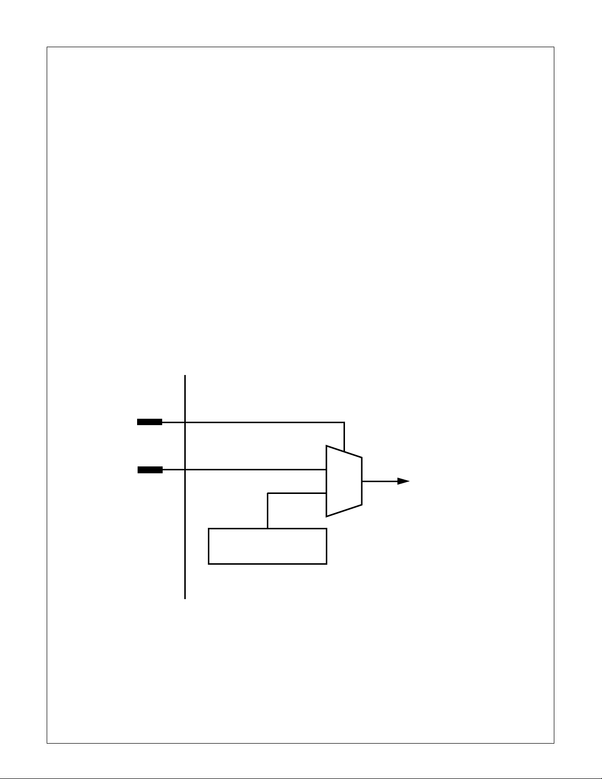
5.9 RESET INTERFACE
The DP83959 LERIC8 has an internal power-on reset function that requires no external components for it to power up
correctly and begin repeater operation automatically.
A TTL compatible reset input is also provided (/MLOAD).
Note that the /MLOAD input is not a Schmitt input: an externally generated pulse must be supplied to this input if it is to
be used. If not required, the /MLOAD input can be left unconnected. A representational logic diagram of the reset
function is given in Figure 4. The RES_INT/EXT pin selects
either internal or external reset.
15
www.national.com
Page 16
5.0 Functional Description (Continued)
Optionally, configuration information can be loaded into the
device at reset from values set by pull-up and/or pull-down
resistors on the D[3:0] and RA[4:0] pins. See Section 5.12
for more details.
The rising edge of the selected reset signal is used to start
the 1 second LED test operation.
As a power-on test feature, the DP83959 will assert all single ended LED outputs, the DP83955/6 compatible LED
outputs and the 'B' outputs of the bi-color LED outputs. The
direct drive LED outputs are asserted during reset as well as
for 1 second following the tr ailing edge of reset, whereas the
DP83955/6 compatible LEDs will only be asserted for the 1
second test, not during reset. See the pin descriptions for
the LEDs in Section 4.3 for more details.
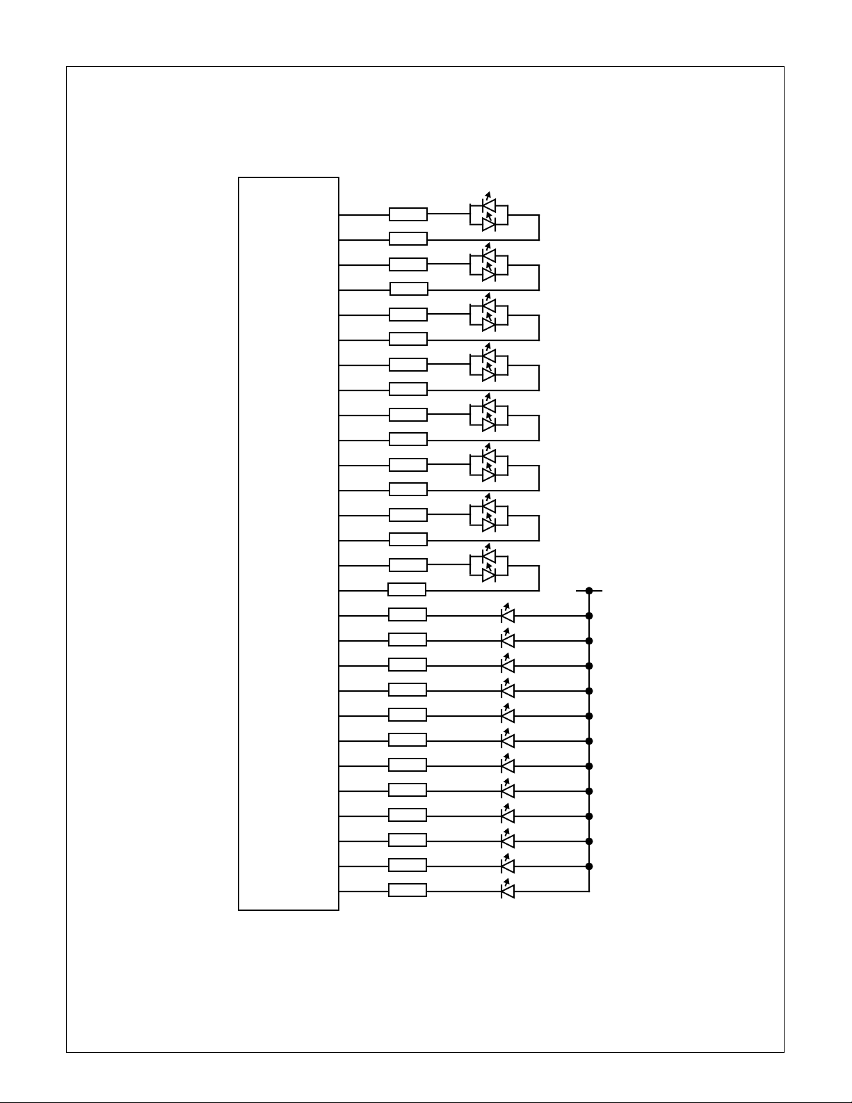
5.10 TRAFFIC MONITOR LED INTERFACE
The Network Traffic Level Monitor function displays the network utilization as a percentage on 8 LEDs connected in
bargraph format. LEDs connected to the /TRAF[1:8] outputs
will indicate the following network traffic le vels 1%, 2%, 3%,
6%, 12%, 25%, 50%, and >80% respectfully . These are chosen in order to provide for an ergonomic display.
The Network T raffic Le vel Monitor function uses a sum of the
internal carrier sense signals from each of the por ts to assess the amount of repeater activity in any given sample pe-
riod. Network activity is sampled at 6.25Hz. The activity
level is decoded into a percentage of the theoretical maximum and output to the /TRAF[1:8] pins for display on the
bargraph style LEDs. That is, all LED outputs up to and including the currently determined network traffic LED level
will be asserted. Figure 5 shows how to connect the traffic
LEDs.
Additionally, three global LEDs are provided:
An Alert LED output indicates when traffic level exceeds
80% for 1 second or more or when any of the eight
10BASE-T ports is par titioned for 1 second or more. The
output will remain active until the excess traffic or long partition event ends or for a minimum of 30ms (nominal value)
to ensure LED visibility.
A global activity LED output (/GACT) indicates the presence
of any receive activity, while a global collision LED output
(/GCOL) indicates the presence of collisions on any port.
These LED outputs have the capability to lengthen the time
the LED is active. At the end of each ev ent, the output is held
asserted for 30 ms, or until another such event occurs .Thus,
at low levels of netw ork activity (f or /GA CT) or netw ork collisions (for /GCOL), the LED is lit long enough to make it discernible to the human eye. At higher rates of events, the
relative brightness of the LEDs indicate high or low activity.
RES_INT/EXT
/MLOAD
Internal Power-On Reset
Pulse Generator
Figure 4. DP83959 Reset Logic
0
1
Internal Reset
Signal
16
www.national.com
Page 17
5.0 Functional Description (Continued)
DP83959
LERIC8
P/L_1A
P/L_1B
P/L_2A
P/L_2B
P/L_3A
P/L_3B
P/L_4A
P/L_4B
P/L_5A
P/L_5B
P/L_6A
P/L_6B
P/L_7A
P/L_7B
P/L_8A
P/L_8B
/TRAF1
/TRAF2
/TRAF3
/TRAF4
/TRAF5
/TRAF6
/TRAF7
/TRAF8
/PART0
/GCOL
/GACT
/ALERT
135Ω (typ.)
135Ω (typ.)
135Ω (typ.)
135Ω (typ.)
135Ω (typ.)
135Ω (typ.)
135Ω (typ.)
135Ω (typ.)
135Ω (typ.)
135Ω (typ.)
135Ω (typ.)
135Ω (typ.)
135Ω (typ.)
135Ω (typ.)
135Ω (typ.)
135Ω (typ.)
270Ω (typ.)
270Ω (typ.)
270Ω (typ.)
270Ω (typ.)
270Ω (typ.)
270Ω (typ.)
270Ω (typ.)
270Ω (typ.)
270Ω (typ.)
270Ω (typ.)
270Ω (typ.)
270Ω (typ.)
G
R
G
R
G
R
G
R
G
R
G
R
G
R
G
R
+5V
Figure 5. DP83959 Direct Drive LED Connections
17
www.national.com
Page 18

5.0 Functional Description (Continued)
5.11 PORT STATUS LEDS
The eight 10BASE-T Port Partition Status/Link OK Status
bi-color LED outputs have the functionality given in Table 2.
The representational logic of this function is given in
Figure 6. This logic is repeated for each of the 10BASE-T
ports ('n' in Figure 6 refers to any of ports 1 through 8). The
DP83959 bi-color LED outputs use two pins each, so that either end of a two-lead bi-color LED may be driven high or
low in order to achieve the required functionality. Two-lead
bi-color LEDs require only the addition of a single series current limiting resistors. Three lead bi-color LEDs must be
driven with two series resistors (one in each cathode lead)
and the common anode lead taken to V
If required, single LEDs may be driven by the bi-color outputs (each taken to V
Figure 5 shows one configuration, using bi-color LEDs.
via an appropriate resistor).
CC
CC
.
5.12 CONFIGURATION/REGISTER INTERFACE
Several operational parameters can be configured into the
LERIC8 at power-on/reset time (optional mode) or the standard LERIC8 configuration can be used (default mode). Selection of the mode is made using the DEF/OPT pin.
For default mode, the DEF/OPT pin must be pulled high (to
V
) with a 4.7 kΩ resistor. In this mode, the LERIC8 uses
CC
the default values given in Table 3.
For optional mode, the DEF/OPT pin must be pulled low. In
this mode, the rising edge of either the internal reset signal
or /MLOAD (see Section 5.9) is used to latch the logic levels
Table 2 10BASE-T Port Status LED Output Functionality Using Bi-color LEDs
held on the D[3:0] and RA[4:0] inputs into the internal configuration registers. Configuration data is set on the D[3:0]
and RA[4:0] pins using 10 kΩ pull-up or pull-down resistors
as required. T ab le 3 shows the parameter sections possible .
A 10 kΩ pull-up resistor to VCC is required to set a configuration bit to 1. A 10 kΩ pull-down resistor to GND to set a
configuration bit to 0.
The LERIC8 has internal registers that are accessible from
the RA[4:0] and D[3:0] interface. A certain amount of control
of operation and status information is available through this
interface. The LERIC8's registers are compatible with those
in the DP83955/6. A full description of the registers is given
in Section 6.0.
Although simple 8-port standalone hubs will not require the
register interface, it was nevertheless included as a necessary factory test feature. In a simple repeater design the /RD
and /WR pins should be disabled by connecting them to
VCC directly or via a suitable pull-up resistor (4.7 kΩ).
Since the RA[4:0] and D[3:0] interface is used for multiple
functions (configuration, register access and Min/Max LED
mode outputs) register read/write data must be transferred
using an external buffer.
The READY pin provides a means of handshaking register
accesses into the LERIC8. A simple programmable logic device (GAL) may be used to decode the address range, assert the appropriate /RD or /WR strobe and check the
READY signal. This provides an appropriate interface for
whatever CPU or other device is connected.
Link Status Port Partition Status LED
Not OK Not Partitioned OFF
Not OK Partitioned OFF
OK Not Partitioned Color #1 (usually GREEN)
OK Partitioned Color #2 (usually YELLOW or RED)
Port Partition Status (1 = Partitioned)
Port Link Status (1 = Link OK)
Figure 6. 10BASE-T Port Status LED Logic Function
P/L_nA
P/L_nB
18
www.national.com
Page 19

5.0 Functional Description (Continued)
Table 3 Default/Optional Mode Configuration Parameter Selection
Pin Function
D0 - - - x Not Used: Don't Care, can leave unconnected.
D1 - - - x Not Used: Don't Care, can leave unconnected.
D2 Reserved Not
D3 EPOLSW Not Selected Selected 1 Enables polarity switching of the receive squelch on
RA0 Reserved Not
RA1 /TXONLY Selected Not Selected 1 Allows the port partition state machines to restrict segment
RA2 /CCLIM 63 31 0 The IEEE802.3 10Mb/s Section 9 repeater partition
RA3 MIN/MAX Minimum
RA4 - - - x Not Used: Don't Care, can leave unconnected.
Effect When
Bit = 0
Permitted
Permitted
Mode
5.13 MIN/MAX MODE LED INTERFACE
The LERIC8 supports the Min and Max LED modes of the
DP83955/6 LERIC devices. If these modes are not required
(for instance, if only the direct drive LED outputs are being
used), then no actions/connections are required. If Min or
Max mode is required, the relevant circuitry is simply added
to the data and address bus pins. The /STR pin is used to
latch data into external latches for display on the status
LEDs.
For Min mode, the LERIC8 operates identically to the
DP83955/6 devices. Table 4 shows the interface pin functions for Min mode.
For Max mode, since the LERIC8 has more ports than the
DP83955/6, a slightly different latching scheme is required.
Figure 7 shows how Max mode functions for the LERIC8.
Data for latching (into external 74x259 addressable latches)
is presented on the D[0:3] and RA0 pins. Address information is presented on the RA[1:4] pins. The address cycles
from 0h through 9h and then returns to 0h and repeats continuously.
5.14 AUI PORT 0
The DP83959 LERIC8 has a single AUI port that uses the
standard 3 differential pairs of signal connections. The AUI
receiver input pairs (RX0+/- and CD0+/-) require external
line termination (78Ω balanced termination). The AUI transmit output pairs utilize class A/B output drivers and do not
require any source termination resistors (as did the
DP83955/6).
Effect When
Bit = 1
Required 1 Reserved: Must be set to 1
Required 1 Reserved: Must be set to 1
Maximum
Mode
Default
Value
detecting polarity reversal of the incoming data.
reconnection only to when a good packet is transmitted on
the partitioned port.
specification requires a port to be partitioned after a certain
number of consecutive collisions. The LERIC8 has two
values availab le to allo w users to customize the partitioning
algorithm to their environment.
1 The operation of the DP83955/6 LERIC compatible LED
display update mode is controlled by this bit.
The three AUI signal pairs (RX, TX, CD) require the use of
an isolation transformer (standard AUI 1:1 type) in order to
meet the fault condition requirements of IEEE 802.3. A typical AUI port connection is shown in Figure 8.
5.15 10BASE-T PORTS 1-8
The DP83959 will directly support up to 8 10BASE-T ports.
Figure 9 shows a typical 10BASE-T port connection.
Each of the 10BASE-T ports uses 4 signal pins on the
DP83959 package (two for transmit outputs and two for receive inputs) plus a shared power and ground. This minimal
configuration is possible due to the 10BASE-T filtering and
waveshaping being implemented internal to the device’s
transmit circuitry. The DP83959 still requires the use of receive filtering and termination and transmit source impedance matching resistors external to the device. Decoupling
capacitors may also be required from the center taps of the
transmit and receive isolation transformers.
On transmit, the 10BASE-T ports of the DP83959 requires
the use of 1:2 step-up transformers in order to generate the
correct transmit output drive voltage. Common mode
chokes may not be required to meet emissions standards if
the layout guidelines are followed.
On receive, the 10BASE-T ports of the DP83959 requires
the use of 1:1 transformers. Filtering may be required to reduce high frequency interference.
Description
19
www.national.com
Page 20

5.0 Functional Description (Continued)
Table 4 LERIC8 Min Mode LED Function
Pin Mnemonic Min Mode Function
D0 ACOL Any Collision: Asserted when a collision occurs on any of this LERIC8's ports.
D1 AREC Any Receive: Asserted when any of this LERIC8's ports experiences a data or collision
packet on its receive inputs.
D2 JAB Jabber: Asserted when this LERIC8 experiences a Jabber protect condition.
D3 APART Any Partition: Asserted when any of this LERIC8's ports is partitioned.
RA[4:0] - No function: Don't care
/STR - Strobe: Used to latch the Min mode information into an external latch (e.g. '374)
DP83959
LERIC8
D0
53
ACOL
-
Port1
LINK
Port2
LINK
Port3
LINK
Port4
LINK
Port5
LINK
Port6
LINK
Port7
LINK
Port8
LINK
D1
D2
D3
RA0
RA1
RA2
RA3
RA4
STR
54
55
56
59
60
61
62
63
36
AREC
JAB
APART
COL
REC
PART
--
0101010101
00110011
000011
0000000011
AUI
AUI
AUI
Port1
COL
Port1
REC
Port1
PART
Port1
BDPOL
Port2
COL
Port2
REC
Port2
PART
Port2
BDPOL
Port3
COL
Port3
REC
Port3
PART
Port3
BDPOL
Port4
COL
Port4
REC
Port4
PART
Port4
BDPOL
Port5
COL
Port5
REC
Port5
PART
Port5
BDPOL
1
Port6
COL
Port6
REC
Port6
PART
Port6
BDPOL
Port7
Port7
Port7
PART
Port7
BDPOL
100
COL
REC
0
Port8
COL
Port8
REC
Port8
PART
Port8
BDPOL
0
Maximum
Mode
LED
Data
(1 indicates
LED ON,
0 indicates
LED OFF)
Maximum
Mode
LED
Address
(Cycles from
0000 to 1001)
Figure 7. LERIC8 Max Mode LED Function/Mapping
20
www.national.com
Page 21

5.0 Functional Description (Continued)
DP83959
LERIC8
TX0+
TX0-
RX0+
RX0-
CD0+
CD0-
39.2Ω ±1%39.2Ω ±1%
0.01µF
39.2Ω ±1% 39.2Ω ±1%
0.01µF
+12V
Fuse
1:1
1:1
1:1
3
DO-A
11
DO-S
10
DO-B
6
Vc
14
VS
5
DI-A
4
DI-S
12
DI-B
7
CO-A
8
CO-S
15
CO-B
2
CI-A
1
CI-S
9
CI-B
13
VP
100pF
AUI Connector
Chassis
DP83959
LERIC8
TXn+
TXn-
RXn+
RXn-
0.1µF
Figure 8. Typical AUI Port Connection
* Starting point values - will need to be
adjusted depending on layout, transformer
module and other application variations.
Transformer
Module
* 13.5Ω
* 820pF
* 820pF
(Only 1 Port shown. All eight 10BASE-T ports are identical to this)
* 13.5Ω
49.9Ω ±1%49.9Ω ±1%
0.01µF
0.01µF
Optional
1:2
1:1
0.01µF
Optional
Common Mode
Choke (Optional)
1
TD+
2
TD-
Connector
3
RD+
6
RD-
RJ45
Figure 9. Typical 10BASE-T Port Connection
21
www.national.com
Page 22

6.0 LERIC8 Registers
6.1 REGISTER ADDRESS MAP
The LERIC8's register address map is shown below. Since
the data path is only a nibble wide interface, each register
has two addresses, with the most significant address bit
(RA4) used to select either the lower or upper nibble of the
register byte information. Each byte wide register can be
thought of as having data bits D[7:0], so that for the lower nibble bits D[3:0] are presented on D[3:0] respectively and for
the upper nibble, bits D[7:4] are presented on D[3:0] respectively. Register descriptions in the following sections are given in the byte wide notation, D[7:0].
Address
RA[4:0]
(4 3210)
Register
0 0000
1 0000
0 0001
1 0001
0 0010
1 0010
0 0011
1 0011
0 0100
1 0100
0 0101
1 0101
0 0110
1 0110
0 0111
1 0111
0 1000
1 1000
0 1001
1 1001
LERIC8 Status - Lower Nibble
LERIC8 Status - Upper Nibble
Port0 (AUI) Status/Config - Lower Nibble
Port0 (AUI) Status/Config - Upper Nibble
Port1 Status/Config - Lower Nibble
Port1 Status/Config - Upper Nibble
Port2 Status/Config - Lower Nibble
Port2 Status/Config - Upper Nibble
Port3 Status/Config - Lower Nibble
Port3 Status/Config - Upper Nibble
Port4 Status/Config - Lower Nibble
Port4 Status/Config - Upper Nibble
Port5 Status/Config - Lower Nibble
Port5 Status/Config - Upper Nibble
Port6 Status/Config - Lower Nibble
Port6 Status/Config - Upper Nibble
Port7 Status/Config - Lower Nibble
Port7 Status/Config - Upper Nibble
Port8 Status/Config - Lower Nibble
Port8 Status/Config - Upper Nibble
22
www.national.com
Page 23

6.0 LERIC8 Registers (Continued)
6.2 LERIC8 STATUS REGISTER
Address: RA4 - RA0
0 0000 - lower nibble
1 0000 - upper nibble
Bit Bit Name Access Bit Description
D0 /ACOL RO Any Collision:
0 = A collision is occurring at one or more of this LERIC8's ports
1 = No collisions
D1 /AREC RO Any Receive:
0 = One of this LERIC8's ports is the current data or collision receiver
1 = No data packet or collision reception within this LERIC8
D2 /JAB RO Jabber Protect:
0 = This LERIC8 has been forced into the Jabber Protect state by one of
its ports or by another port on another LERIC8 connected to this LERIC8's
Inter-LERIC bus
1 = No Jabber Protect conditions exist currently
D3 /APART RO Any Partition:
0 = One or more ports of this LERIC8 are partitioned
1 = No ports are partitioned
D4 Reserved RO Reserved - Don't care
D5 Reserved RO Reserved - Don't care
D6 Reserved RO Reserved - Don't care
D7 Reserved RO Reserved - Don't care
Key: RO = Read Only, R/W = Read Write.
23
www.national.com
Page 24

6.0 LERIC8 Registers (Continued)
6.3 PORT 0 (AUI) STATUS/CONFIGURATION REGISTER
Address: RA4 - RA0
0 0001 - lower nibble
1 0001 - upper nibble
Bit Bit Name Access Bit Description
D0 Reserved RO Reserved - Don't care
D1 /COL RO Collision:
0 = A collision is happening or occurred during the current packet
1 = No collisions have occurred (as yet) in the current packet
D2 /REC RO Receive:
0 = This port is now, or has been, the receive source of data packet or
collision information for the current network event
1 = This port is not, and has not been, the receive source for the current
network event
D3 /PART R/W Partition:
0 = This port is currently partitioned
1 = This port is not currently partitioned
Writing a 1 to this bit forces segment reconnection and partition state
machine reset. Writing a 0 to this bit has no effect.
D4 Reserved RO Reserved - Don't care
D5 Reserved RO Reserved - Don't care
D6 Reserved RO Reserved - Don't care
D7 DISPT R/W Disable Port:
0 = Port operates as defined by normal repeater operations
1 = All port activity is prevented
Key: RO = Read Only, R/W = Read Write.
24
www.national.com
Page 25

6.0 LERIC8 Registers (Continued)
6.4 PORTS 1-8 (10BASE-T) STATUS/CONFIGURATION REGISTERS
Address: RA4 - RA0
0 0010 to 0 1001 - lower nibble
1 0010 to 1 1001 - upper nibble
Bit Bit Name Access Bit Description
D0 /GDLNK R/W Good Link:
0 = Link pulses are being received by this port
1 = Link pulses are not being received by this port
Writing a 1 to this bit will cause the 10BASE-T transceiver not to
transmit or monitor the reception of link pulses. Writing a 0 to this bit
will return the 10BASE-T transceiver to normal operation.
D1 /COL RO Collision:
0 = A collision is happening or occurred during the current packet
1 = No collisions have occurred (as yet) in the current packet
D2 /REC RO Receive:
0 = This port is now, or has been, the receive source of data packet or
collision information for the current network event
1 = This port is not, and has not been, the receive source for the
current network event
D3 /PART R/W Partition:
0 = This port is currently partitioned
1 = This port is not currently partitioned
Writing a 1 to this bit forces segment reconnection and partition state
machine reset. Writing a 0 to this bit has no effect.
D4 SQL R/W Squelch Level:
0 = This port's 10BASE-T transceiver operates with normal IEEE
defined receive squelch level
1 = This port's 10BASE-T transceiver operates with reduced receive
squelch level
D5 POL RO Polarity:
0 = This port's receive polarity is normal (not inverted)
1 = This port's receive polarity is inverted
D6 Reserved R/W Reserved:
1 = LERIC8 factory test mode - Do not use.
D7 DISPT R/W Disable Port:
0 = Port operates as defined by normal repeater operations
1 = All port activity is prevented
Key: RO = Read Only, R/W = Read Write.
25
www.national.com
Page 26

7.0 System Considerations
The DP83959 can be designed into several types of repeaters. The most common design is the unmanaged,
stand-alone, 8-port repeater, where a single LERIC8 will be
used to provide the repeater capabilities. For designs that require more than 8 ports, up to 3 LERIC8s may be cascaded
on a single board.
7.1 CASCADING
Figure 10 shows the connection diagram for using 3
DP83959s in a single repeater. Most of the inter-LERIC bus
is tied together. /ACKO of one device is connected to /ACKI
of the next one. /ACKI on one end of the chain is tied high,
while /ACKO on the other end is a no-connect.
7.2 IEEE CONFORMANCE
The LERIC8 was tested for IEEE 802.3 conformance in a repeater system. Without any resistive loading on the RTX and
REQ pins, the repeater passed all conformance tests with
the exception of P eak Differential Output Voltage (V
resistive load). With only one twisted pair port loaded and
transmitting a packet, with the system running at 5.25 V in a
o
0
C chamber, the output violated the Peak Differential Out-
put V oltage (V
into a resistive load) marginally at the upper
OD
limit. With all eight twisted pair ports loaded and transmitting,
and with the system running at 4.75 V in a 80
the output violated the Peak Diff erential Output Voltage (V
into a resistive load) marginally at the lower limit. Performance is also dependent on PCB layout.
into a
OD
o
C chamber,
OD
The violation of this specification under these conditions will
not affect a normal network. The LERIC8 passes the IEEE
Output Waveform with Scaling Voltage template and the inverted template, both of which specify V
at the end of a ca-
OD
ble. The LERIC8 has also undergone endurance testing in
various platforms and has not shown any loss of data.
The RTX and REQ pins can be used to tune the internal
transmit filter and wave shaping circuitry. The RTX input can
be used to adjust the differential voltage (V
output drivers. By placing a resistor between RTX and V
) of all of the
OD
CC
the peak-to-peak voltage will be increased. Conversely, connecting the resistor to GND will decrease V
OD
.
The REQ input can be used to adjust the shape of the waveform for all outputs. By placing a resistor between REQ and
V
, the amplitude of the pre-emphasis waveform will be in-
CC
creased. Conversely, connecting the resistor to GND will decrease the amplitude.
Caution should be taken when using RTX and REQ to make
adjustments. The following IEEE parameters may be adversely affected by adjusting the amplitude or shape of the
transmitted waveform, as well as PCB layout and design:
Peak Differential Output Voltage, Harmonic Content, Output
wavef orm with Scaling of V oltage template, Output Wa veform
with Scaling of V oltage inv erted template, TD circuit Differential Output Impedance, T r ansmit Output Timing Jitter with Cable Model, and Transmit Output Timing Jitter without Cable
Model.
,
4.7K
IRD
IRC
/IRE
/ACKI
STATUS LEDS
/ACTN
/COLN
/ACKO
/ANYXN
PARTITION/LINK LEDS
TRAFFIC LEDS
GLOBAL LEDS
IRD
IRC
/IRE
/ACKI
STATUS LEDS
/ACTN
/COLN
/ACKO
/ANYXN
PARTITION/LINK LEDS
680 680
680
680
IRD
IRC
/IRE
/ACKI
/ACTN
/COLN
STATUS LEDS
PARTITION/LINK LEDS
N.C.
/ACKO
/ANYXN
Figure 10. Connection Diagram for Cascading
26
www.national.com
Page 27

8.0 DC Specifications
Absolute Maximum Ratings
Supply Voltage (VCC) -0.5V to 7.0V
DC Input Voltage (V
DC Output Voltage (V
Power Dissipation (P
Storage Temperature Range (T
Lead Temp. (T
ESD Rating
= 1.5k, C
(R
ZAP
) -0.5V to VCC + 0.5V
IN
) -0.5V to VCC + 0.5V
OUT
) (Note 1) 4.5 W
D
) -65°C to 150°C
STG
) (Soldering, 10 sec) 260°C
L
2.0 kV
= 120 pF)
ZAP
Recommended Operating Conditions
Supply Voltage (VCC) 5 Volts + 5%
Ambient Temperature (T
Note:
Absolute maximum ratings are those values beyond
which the safety of the device cannot be guaranteed. They
are not meant to imply that the device should be operated at
these limits.
) 0 to 70°C
A
DC Specifications
TA = 0°C to 70°C, VCC = 5V ± 5% unless otherwise specified
Symbol Description Conditions Min Typ Max Units
PROCESSOR, LED, AND INTER-LERIC INTERFACES
V
OH
V
OL
V
V
I
IN
I
OZ
I
CC
AUI (PORT 0)
Minimum High Level Output Voltage IOH= -8 mA 3.5 V
Minimum Low Level Output Voltage IOL = 8 mA 0.4 V
Minimum High Level Input Voltage 2.0 V
IH
Maximum Low Level Input Voltage 0.8 V
IL
Input Current VIN = VCCor GND -1.0 1.0 µA
Maximum TRI-STATE Output Leakage
Current
Average supply current VIN = VCCor GND
V
= VCCor GND -10 10 µA
OUT
570 800 mA
V
= 5.25V
CC
V
OD
V
OB
V
V
DS
V
CM
Differential Output Voltage (TX ±)78Ω Termination ± 550 ± 1200 mV
Differential Output Voltage Imbalance (TX ±)
78Ω Termination 40 mV
(Note 2)
Undershoot Voltage (TX ±) (Note 2) 78Ω Termination 80 mV
U
Differential Squelch Threshold (RX ±, CD ±) -175 -300 mV
Differential Input Common Mode Voltage
0 5.5 V
(RX ±, CD ±) (Note 2)
10BASE-T (PORTS 1-8)
V
RON
Note 1: This value is the absolute maximum, and not intended to be used to calculate case temperature. A value of 1.8W can be used for the purpose of device
heat calculations.
Note 2: This parameter is guaranteed by design and is not tested.
Note 3: The operation in Reduced mode is not gauranteed below 300 mV.
Minimum Receive Squelch Threshold:
Normal Mode
Reduced Mode
± 300
(Note 3)
± 585
± 340
mV
mV
27
www.national.com
Page 28

9.0 Switching Characteristics
9.1 PORT ARBITRATION
/ A C K I
T1 T2
/ A C K O
Number Symbol Parameter Min Max Units
T1
T2
Note: Timing valid with no receive or collision activities.
ackilackol
ackihackoh
/ACKI Low to /ACKO Low
/ACKI High to /ACKO High
26
23
9.2 RECEIVE - AUI PORT
Receive activity propagation start up and end delays for the AUI port.
R X
T5a
T6a
/ A C T N
T3a
T4a
/ A C K O
Number Symbol Parameter Min Max Units
ns
ns
T3a
T4a
T5a
T6a
Note: /ACKI assumed high.
Note 1: This time includes EOP.
Note 2: This parameter assumes squelch triggers on negative edge of RX data.
rxaackol
rxiackoh
rxaactnl
rxiactnh
RX Active to /ACKO Low (Note 2)
RX Inactive to /ACKO High (Note 1)
RX Active to /ACTN Low (Note 2)
RX Inactive to /ACTN High (Note 1)
28
66
235
75
235
www.national.com
ns
ns
ns
ns
Page 29
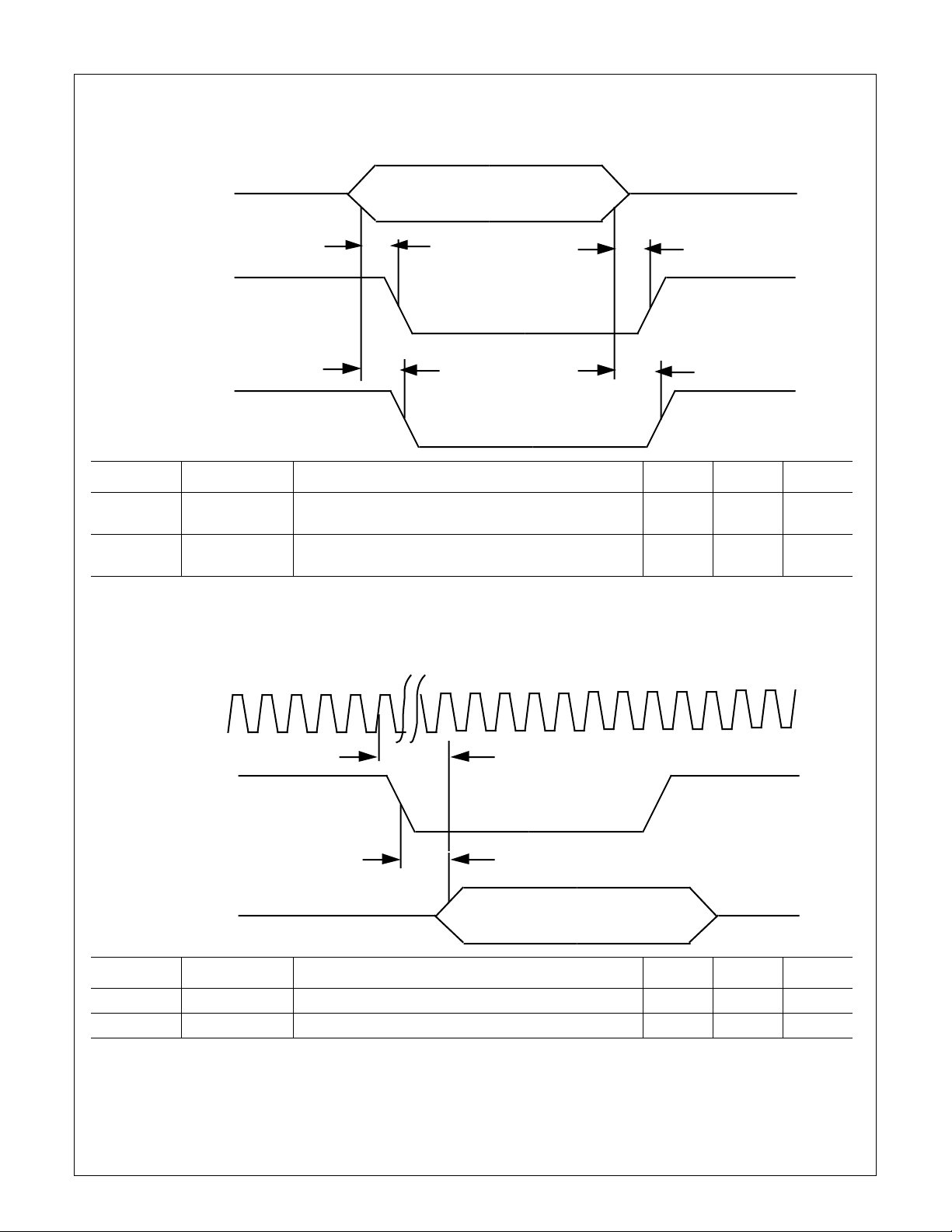
9.0 Switching Characteristics (Continued)
9.3 RECEIVE - 10BASE-T PORTS
Receive activity propagation start up and end delays for 10BASE-T ports.
R X
T5t
T6t
/ A C T N
T3t
T4t
/ A C K O
Number Symbol Parameter Min Max Units
T3t
T4t
T5t
T6t
Note: /ACKI assumed high.
Note 1: This time includes EOP.
rxaackol
rxiackoh
rxaactnl
rxiactnh
RX Active to /ACKO Low
RX Inactive to /ACKO High (Note 1)
RX Active to /ACTN Low
RX Inactive to /ACTN High (Note 1)
300
280
300
280
9.4 TRANSMIT - AUI PORT
Transmit activity propagation start up and end delays for the AUI port.
ns
ns
ns
ns
CLOCK
T16 a
/ A C T N
T15 a
T X
Number Symbol Parameter Min Max Units
T15a actnltxa /ACTN Low to TX Active 675 ns
T16a clkitxa CLOCK in to TX Active 45 ns
Note: /ACKI assumed high.
29
www.national.com
Page 30
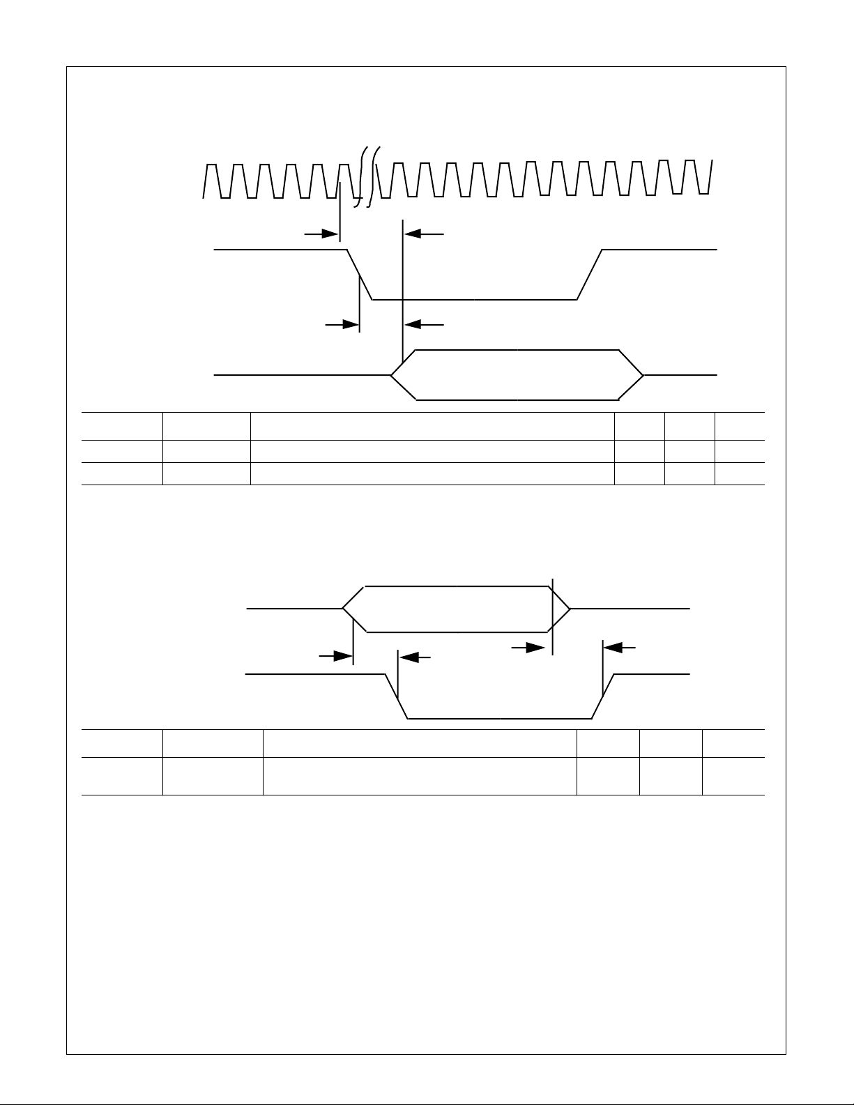
9.0 Switching Characteristics (Continued)
9.5 TRANSMIT - 10BASE-T PORTS
Receive activity propagation start up and end delays 10BASE-T ports.
CLOCK
T16 t
/ A C T N
T15 t
T X
Number Symbol Parameter Min Max Units
T15t actnltxa /ACTN Low to TX Active 790 ns
T16t clkitxa CLOCK in to TX Active 45 ns
Note: /ACKI assumed high.
9.6 COLLISION - AUI PORT
Collision activity propagation start up and end delays for the AUI port.
9.6.1 Transmit Collisions
C D
T30a
T31a
/ A N Y X N
Number Symbol Parameter Min Max Units
T30a
T31a
Note 1: TX collision extension has already been performed and no other port is driving /ANYXN.
Note 2: Includes TW2.
cdaanyxnl
cdianyxnh
CD Active to /ANYXN Low
CD Inactive to /ANYXN High (Note 1,2)
85
285
ns
ns
30
www.national.com
Page 31

9.0 Switching Characteristics (Continued)
9.6.2 Receive Collisions
C D
T32 a
T33 a
/ C O L N
T39
T40
T X DATA JAM
Number Symbol Parameter Min Max Units
T32a
T33a
T39
T40
Note 1: Reception ended before /COLN goes high.
cdacolna
cdicolni
colnljs
colnhje
CD Active to /COLN Low
CD Inactive to /COLN High
/COLN Low to Start of JAM
/COLN High toEnd of JAM (Note 1)
75
215
400
585
9.7 COLLISION - 10BASE-T PORTS
Collision activity propagation start up and end delays for 10BASE-T ports
T X
ns
ns
ns
ns
R X
T30 t
T31 t
/ A N Y X N
Number Symbol Parameter Min Max Units
T30t
T31t
Note 1: TX collision extension has already been performed and no other port is asserting /ANYXN.
colaanyl
colianyh
Collision Active to /ANYXN Low
Collision Inactive to /ANYXN High (Note 1)
800
450
ns
ns
31
www.national.com
Page 32
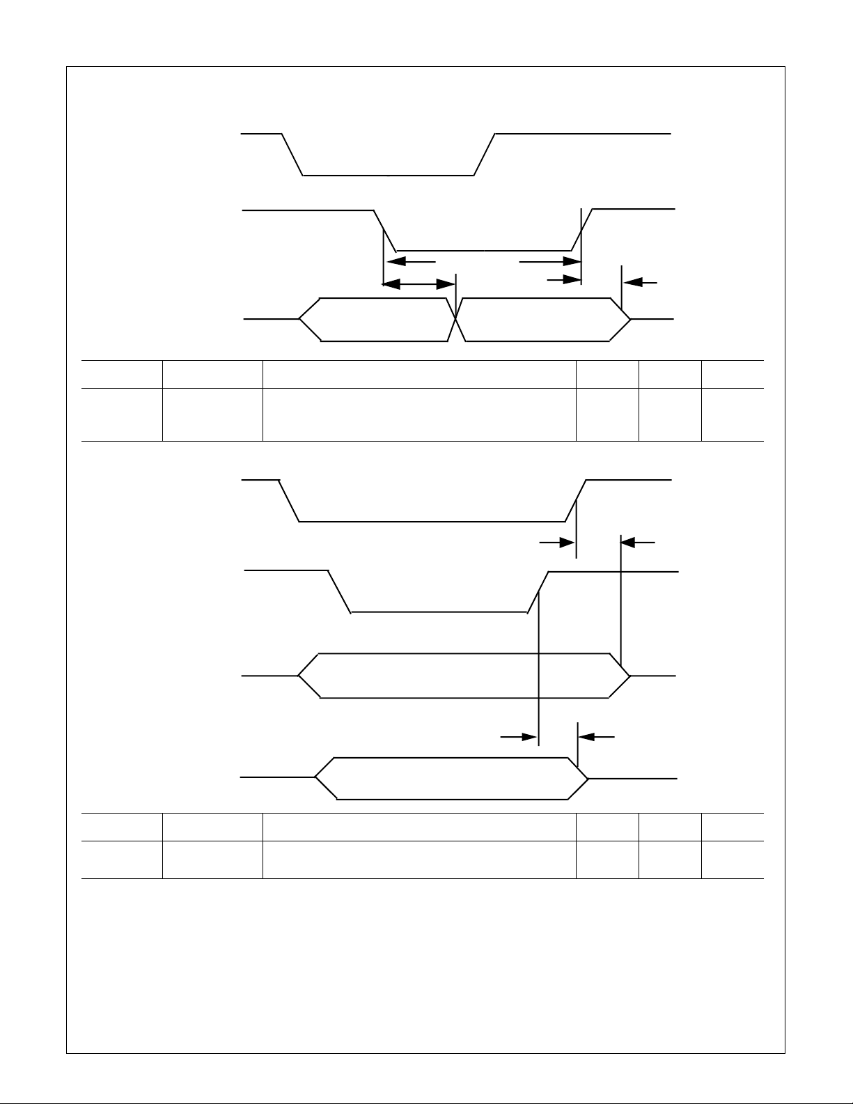
9.0 Switching Characteristics (Continued)
9.8 COLLISION - ALL PORTS - INTER-LERIC BUS
/ A C T N
/ A N Y X N
T38
T34
T35
T X
Number Symbol Parameter Min Max Units
T34
T35
T38
anylmin
anyhtxai
anylsj
/ANYXN Low time
/ANYXN High to TX to all Inactive
/ANYXN Low to Start of JAM
DATA JAM
960
20 370
565
9.9 COLLISION - ALL PORTS - ONE PORT LEFT
/ A C T N
T36
/ A N Y X N
ns
ns
ns
T X
T37
T X
one port left
Number Symbol Parameter Min Max Units
T36
T37
Note: 96 bits of JAM have already been propagated.
actnhtxi
anyhtxoi
/ACTN High to TX Inactive
/ANYXN High to TX 'One Port Left' Inactive 20
32
410
200
www.national.com
ns
ns
Page 33
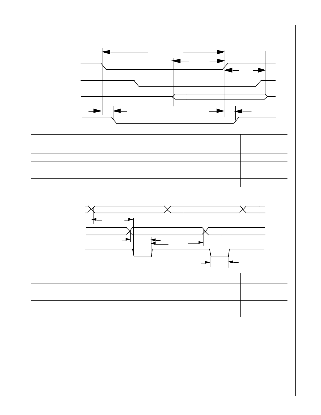
9.0 Switching Characteristics (Continued)
9.10 RESET
/ MLOAD
** / MLOAD_INT
D( 7 : 0 )
T65
T61
T62
T63
T64
/ B U F E N
** /MLOAD_INT is the internal signal which is delayed 5 cycles from the external /MLOAD signal
Number Symbol Parameter Min Max Units
T61 resdats Data Setup 20 ns
T62 resdath Data Hold 20 ns
T63 reslbufl /MLOAD Low to /BUFEN Low 35 ns
T64 reshbufh /MLOAD High to /BUFEN High 35 ns
T65 resw /MLOAD Width 800 ns
9.11 LED STROBE
RA( 4:1 )
(address)
T66
RA( 0 )
D( 3: 0 )
(data)
T67
T68
/ S T R
T69
Number Symbol Parameter Min Max Units
T66 stradrs Strobe Address Setup 70 100 ns
T67 strdats Strobe DATA SETUP 35 55 ns
T68 strdath Strobe Data Hold 145 165 ns
T69 strw Strobe Width 30 65 ns
33
www.national.com
Page 34

9.0 Switching Characteristics (Continued)
9.12 REGISTER READ
/ R D
T82
T88
T83
/ B U F E N
T89
T80
RA( 4:0 )
(address)
T84
T81
T85
D( 3: 0 )
(data)
T87
/ R DY
Number Symbol Parameter Min Max Units
T80
T81
T82
T83
T84
T85
T86
T87
T88 rdw /RD Width 650 ns
T89 rdtr /RD Low to D(3:0) TRI-STATE 80 355 ns
rdadrs
rdadrh
rdlbufl
rdhbufh
bufldatv
rddath
rdlrdyl
rdhrdyh
Address Setup from /BUFEN Low
Address Hold after /RD High
/RD Low to /BUFEN Low
/RD High to /BUFEN High
/BUFEN Low to Data Valid
Data Hold After /RD High 60
/RD Low to /RDY Low
/RD High to /RDY High
T86
0
0
80 355
340 585
85 ns
35
190 ns
30
ns
ns
ns
ns
ns
ns
Note: Minimum high time between read/write cycles is 100 ns.
34
www.national.com
Page 35
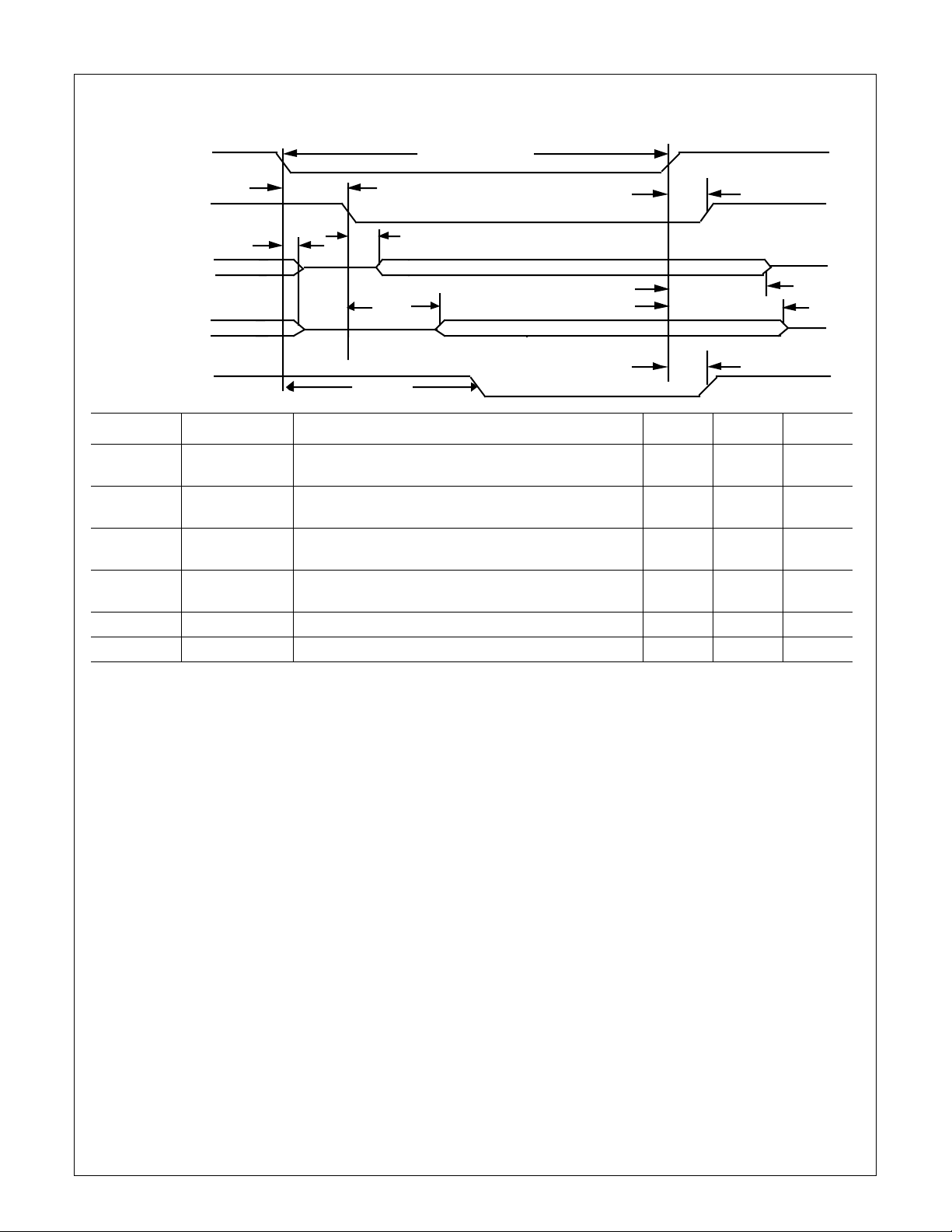
9.0 Switching Characteristics (Continued)
9.13 REGISTER WRITE
/ W R
T92
T98
T93
/ B U F E N
T99
T90
RA( 4:0 )
(address)
T94
T91
T95
D( 3:0 )
(data)
T96
T97
/ R DY
Number Symbol Parameter Min Max Units
T90
T91
T92
T93
T94
T95
T96
T97
T98 wrw /WR Width 650 ns
T99 wrtr /WR Low to D(3:0) TRI-STATE 80 355 ns
wradrs
wradrh
wrlbufl
wrhbufh
wradatv
wrdath
wrlrdyl
wrhrdyh
Address Setup from /BUFEN Low
Address Hold after /WR High
/WR Low to /BUFEN Low
/WR High to /BUFEN High
/BUFEN Low to Data Valid
Data Hold After /WR High 0
/WR Low to /RDY Low
/WR High to /RDY High
T96
0
0
80 355
340 585
14 ns
35
160 ns
30
ns
ns
ns
ns
ns
ns
Note: Minimum high time between read/write cycles is 100 ns.
35
www.national.com
Page 36

9.0 Switching Characteristics (Continued)
9.14 INTER-LERIC BUS (PACKET OUTPUT)
/ A C T N
//
//
//
T105
////
/ I R E
T106
I R C
//
T108
T107
I R D
Number Symbol Parameter Min Max Units
T101 ircoh IRC Output Duty Cycle High Time 40 60 %
T102 ircol IRC Output Duty Cycle Low Time 40 60 %
T103 ircoc IRC Output Cycle Time 90 110 ns
T105 actnolireol /ACTN Output Low to /IRE Output Low 500 ns
T106 ireolirca /IRE Output Low to IRC Active 1.8 µs
T107 irdov IRD Output Valid from IRC 10 ns
T108 irdos IRD Output Stable Valid Time 90 ns
T109 ircohireh IRC Output High to /IRE High 30 70 ns
T110 ircclks Number of IRCs after /IRE high 5 clks
//
//
T109
T110
//
//
T101
T102
T103
//
//
9.15 INTER-LERIC BUS (PACKET INPUT)
/ I R E
//
//
//
T116
I R C
//
//
//
T111
T114
T112
T115
I R D
Number Symbol Parameter Min Max Units
T111 ircih IRC Input High Time 20 ns
T112 ircil IRC Input Low Time 20 ns
T114 irdisirc IRD Input Setup to IRC 5 ns
T115 irdihirc IRD Input Hold from IRC 10 ns
T116 ircihireh Set Up Time of the Rising Edge of IRE to the Rising
//
Edge of IRC for End of Packet Generation
//
25 75 ns
//
36
www.national.com
Page 37

10.0 AC Timing Test Conditions
10.1 GENERAL TEST CONDITIONS
All AUI specifications are valid only if the mandatory isolation
transformer is employed and all differential signals are measured at the AUI connector (not at the DP83959 LERIC8 directly).
0.1 µF
V
CC
S (Note 2)
Input Pulse Levels (TTL/CMOS) GND to 3.0V
Input Rise and Fall Times
5 ns
(TTL/CMOS)
Input and Output
1.5V
Reference Levels (TTL/CMOS)
Input Pulse Levels (Differential) -350 to -1315 mV
Input and Output
Reference Levels (Diff.)
50% Point of
the Differential
TRI-STATE Reference Levels Float (∆V) ± 0.5V
Output Load (See
Figure
below)
DEVICE
R = 2.2 kΩ
UNDER
TEST
C (Note 1)
Note 1: 100 pF, includes scope and test jig capacitance.
Note 2: S1 = Open during timing tests for push pull outputs.
for VOL test.
S1 = V
CC
S1 = GND for V
S1 = V
CC
Impedance measurements.
S1 = GND for High Impedance to active high, and active high to High
Impedance measurements.
test.
OH
for High Impedance to active low, and active low to High
10.2 CAPACITANCE
TA = 25°C, f = 1 MHz
Symbol Parameter Typ Units
Input Capacitance 7 pF
Output Capacitance 7 pF
C
C
OUT
IN
37
www.national.com
Page 38

11.0 Physical Dimensions inches (millimeters) unless otherwise noted
DP83959 8-Port Lite Ethernet Repeater Interface Controller
Molded Plastic Quad Flat Package, JEDEC
Order Number DP83959VUL
NS Package Number VUL160A
LIFE SUPPORT POLICY
NATIONAL’S PRODUCTS ARE NOT AUTHORIZED FOR USE AS CRITICAL COMPONENTS IN LIFE SUPPORT
DEVICES OR SYSTEMS WITHOUT THE EXPRESS WRITTEN APPROVAL OF THE PRESIDENT OF NA TIONAL SEMICONDUCTOR CORPORATION. As used herein:
1. Life support devices or systems are devices or systems
which, (a) are intended for surgical implant into the body,
or (b) support or sustain life, and whose failure to perform, when properly used in accordance with instructions
2. A critical component is any component of a life support
device or system whose failure to perform can be reasonably expected to cause the failure of the life support
device or system, or to affect its safety or effectiveness.
for use provided in the labeling, can be reasonably expected to result in a significant injury to the user.
National Semiconductor
Corporation
Tel: 1-800-272-9959
Fax: 1-800-737-7018
Email: support@nsc.com
National Semiconductor
Europe
Fax: (+49) 0-180-530 85 86
Email: europe.support@nsc.com
Deutsch Tel: (+49) 0-180-530 85 85
English Tel: (+49) 0-180-532 78 32
NNational Semiconductor
Asia Pacific
Customer Response Group
Tel: 65-254-4466
Fax: 65-250-4466
Email: sea.support@nsc.com
National Semiconductor
Japan Ltd.
Tel: 81-3-5620-6175
Fax: 81-3-5620-6179
www.national.com
National does not assume any responsibility for use of any circuitry described, no circuit patent licenses are implied, and National reserves the right, at any time without notice, to change said circuitry or specification.
 Loading...