

Page 1
PRELIMINARY
DP83953 (RIC2A)
Repeater Interface Controller with Security Features,
Internal Drivers and Integrated Filters
DP83953 (RIC2A) Repeater Interface Controller with Security Features, Internal Drivers and Integrated Filters
March 1998
General Description
The DP83953 Repeater Interface Controller with Security
Features and Integrated Transmit Filters (RIC2A) is an enhanced v ersi on of t he DP83952 Repeat er Inter f ace Control ler with Security Features (RIC II). The RIC2A integrates
driver and f il ter circuitry into the RIC II design.
The functionality of the RIC2A is essentially similar to the
RIC II, but the pin definitions have been modified to reflect
the added integrated drivers and filters. Additionally, the
power and ground pin locations have been rearranged.
Therefore, the RIC2A is not a drop in replacement for the
RIC ll.
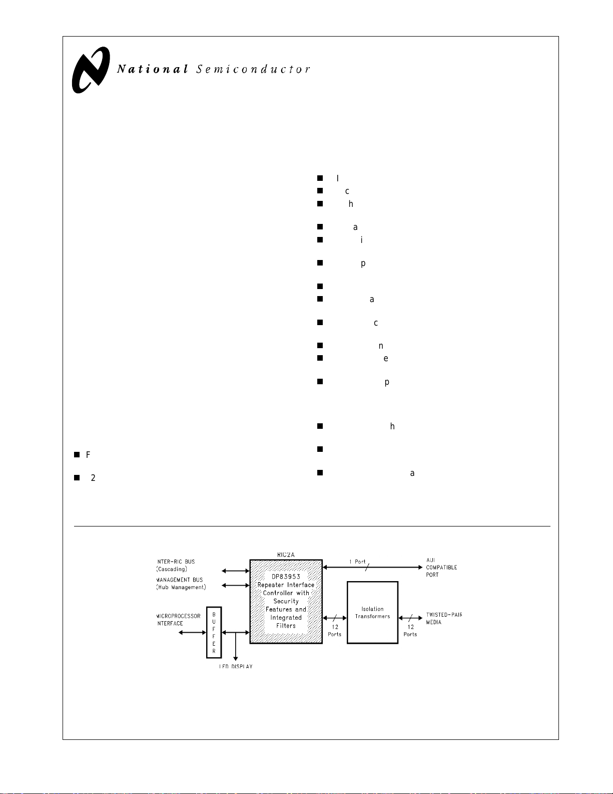
The RIC2A is National Semiconductor’s managed repeater
solution designed to comply with IEEE 802.3 Repeater
Specifica tions. Segment partiti on and jabber loc kup protection state machines are implemented in accordance with
this standard. The RIC2A has thirteen network interface
ports available, including an AUI compatible port. The AUI
port incorporates driv ers to connect an ext ernal MAU using
maximum length cable. Similarly, the other twelve interface
ports integrat e 10BASE- T t ransc eiv ers with supporting dri ver and transmit filter circuitry. (continued)
Features
Fully compliant with the IEEE 802.3 Repeater Specification
12 IEEE 802.3 10BASE-T compatible ports with built-in
drivers and analog transmit filters; additional external
isolation transformers are required to implement hubs
1 IEEE 802.3 compatible AUI port
Cascadable for la rger hub applications
On chip Elasticity Buffer, Manchester encoder and decoder
Separate Partition state machines for each port
Compatible with 802.3k Hub Management requirements
LED displays to provide port status information, including receive, collision, partition, jabber and link status,
Power-up configuration options
Repeater and Partition Specifications, Status Display,
Processor Operati ons
Simple processor interface for repeater management
and port disable.
On-chip Event Counte rs and Event Flag Arrays
Serial Management Bus Interface to combine packet
and repeater status information
Single 5V supply
The Security Features
Prevents unauthorized eavesdropping and/or intrusion
on a per port basis
58 On Chip CAMs (Content Addressable Memory) allow storage of acceptable addresses
Learn mode automatically records addresses of attached node
System Diagram
FAST® and TRI-STATE® are registered trademarks of National Semiconductor Corporation.
™
is a trademark of National Semiconductor Corporation
100RIC
™
SONIC
is a trademark of National Semiconductor Corporation
Ethernet is a trademark of Xerox Corporation
is a registered trademark of Lattice Semiconductor
GAL
®
PAL
is a registered trademark of and license from Advanced Micro Devices, Inc.
®
© 1998 National Semiconduct or Corporation
www.national.com
Page 2

General Description
(continued)
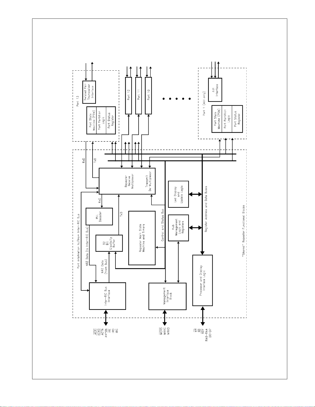
The RIC2A repeater consists of two major functional
blocks: The segment specific block and the shared functional b locks. The segment specific b lock incorporates relevant IEEE specifications on a per port basis. The shared
functional bl ocks incorporate core logic for the entire IEEE
repeater unit. The core logic blocks consist of a repeater
receive multiple xor, a phase locked loop (PLL), a Manches ter decoder, an elasticity buffer, a transmit encoder and a
demultip lexor.
A larger repeater system may be constructed by cascading
several RIC2A devices via the Inter-RIC bus. This method
Table of Contents
1.0 Connection Diagram . . . . . . . . . . . . . . . . . . . . . . . . . . . 3
2.0 Pin Descriptions . . . . . . . . . . . . . . . . . . . . . . . . . . . . . . . 5
3.0 Block Diagrams . . . . . . . . . . . . . . . . . . . . . . . . . . . . . . 10
4.0 Functional Description . . . . . . . . . . . . . . . . . . . . . . . . . 12
4.1 Summary of DP83953 RIC2A Feature
Enhancements from DP83952 RIC II . . . . . . . . . 12
4.2 Overview Of RIC2A Functions . . . . . . . . . . . . . . . 12
4.3 Description Of Repeater Operations . . . . . . . . . . 14
4.4 Examples Of Packet Repetition
Scenarios . . . . . . . . . . . . . . . . . . . . . . . . . . . . . . . 19
4.5 Description Of Hardware Connection For Inter-ric
Bus . . . . . . . . . . . . . . . . . . . . . . . . . . . . . . . . . . . . 27
4.6 Processor and Display Interface . . . . . . . . . . . . . 28
4.7 Description Of Hardware Connection For Processor
And Display Interface . . . . . . . . . . . . . . . . . . . . . . 30
of cascading allows the RIC2A system to function as a single repeater unit without introducing additional repeater
hops.
The RIC2A is configurable for specific applications. It provides port status information for LED array displays and a
simple interface for system processors. The RIC2A possesses multifunctional counters and status flag arrays to
facilitate network statistics gathering, as well as a serial
Hub Management Interf ace Bus for collect ing, e v ent dat a in
managed hub applications.
5.0 HUB Management Support . . . . . . . . . . . . . . . . . . . . . 35
5.1 Event Counting Function . . . . . . . . . . . . . . . . . . 35
5.2 Event Record Function . . . . . . . . . . . . . . . . . . . . 36
5.3 Management Interface Operation . . . . . . . . . . . . 37
5.4 Description of Hardware Connection for
Management Interface . . . . . . . . . . . . . . . . . . . . 43
6.0 Port Block Functions . . . . . . . . . . . . . . . . . . . . . . . . . 44
6.1 Transceiver Functions . . . . . . . . . . . . . . . . . . . . 44
6.2 Segment Partition . . . . . . . . . . . . . . . . . . . . . . . . 47
6.3 Port Status Register Functions . . . . . . . . . . . . . . 47
6.4 Local Ports and Expected Activity . . . . . . . . . . . 49
7.0 RIC2A Registers . . . . . . . . . . . . . . . . . . . . . . . . . . . . . 50
8.0 Board Layout Recommendations . . . . . . . . . . . . . . . 75
9.0 DC and AC Specification . . . . . . . . . . . . . . . . . . . . . . 77
10.0 Physical Dimensions . . . . . . . . . . . . . . . . . . . . . . . . . 90
2 www.national.com
Page 3
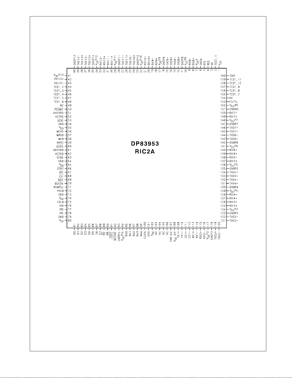
1.0 Connection Diagram
Order Number DP83953VUL
NS Package Number VUL160A
3 www.national.com
Page 4

1.0 Connection Diagram
(Continued)
12 T.P. Ports + 1 AUI
PIN NAME PIN NO. PIN NAME PIN NO. PIN NAME PIN NO. PIN NAME PIN NO.
GNDP13 40 V
DD
TXO13- 39 GND 79 TXO2+ 119 TEST_11 159
TXO13+ 38 IRC 78 GNDP2 118 TES T_10 158
TXO12- 37 IRE 77 V
TXO12+ 36 IRD 76 RXI2- 116 TEST_8 156
GNDP12 35 COLN 75 RXI2+ 115 TEST_7 155
P12 34 V
V
DD
DD
RXI12- 33 GND 73 RX1+ 113 FIL TTL 153
RXI12+ 32 PKEN 72 CD1- 112 V
RXI11- 31 RXMPLL 71 CD1+ 111 GNDWS 151
RXI11+ 30
V
P11 29
DD
GNDP11 28
TXO11- 27
TXO11+ 26
TXO10- 25 V
BUFEN
RDY
ELI
RTI
STR0
DD
TXO10+ 24 GND 64 NC 104 TXO6- 144
GNDP10 23
P10 22 ACTND 62 V
V
DD
STR0
RXI10- 21 ANYXND 61 GND 101 V
RXI10+ 20
ACKO
RXI9- 19 MRXC 59 RA4 99 RXI6+ 139
RXI9+ 18 MEN 58 RA3 98 RXI5- 138
P9 17 MRXD 57 RA2 97 RXI5+ 137
V
DD
GNDP9 16 MCRS 56 RA1 96 V
TXO9- 15 V
DD
TXO9+ 14 GND 54 V
TXO8- 13
ACKI
TXO8+ 12 ACTNS 52
GNDP8 11 ANYXNS 51
P8 10
V
DD
PCOMP
RXI8- 9 NC 49
RXI8+ 8 TEST_6 48 D7 88 RXI4- 128
V
A 7 TEST_5 47 D6 87 RXI4+ 127
DD
GNDA 6 TEST_4 46 D5 86 RXI3- 126
RTX 5 TEST_3 45 D4 85 RXI3+ 125
REQ 4 TEST_2 44 D3 84 V
NC 3 RXI13- 43 D2 83 GNDP3 123
TEST_1 2 RXI13+ 42 D1 82 TXO3- 122
V
DD
Note 1: NC = No Connect
Note 2: Port
Note 3: The path to each port
V
1V
and GND are denoted as
DD
V
and GND must have a very low impedance.
DD
P13 41 D0 81 TXO3+ 121
DD
V
Px and GNDPx, where x=2-13 for all twisted pair ports.
DD
80 TXO2- 120 GND 160
P2 117 TEST_9 157
DD
74 RX1- 114 NC 154
WS 152
DD
70 TX1- 110 RXI7- 150
69 TX1+ 109 RXI7+ 149
68 VDD AUI 108 VDDP7 148
67 GND AUI 107 GNDP7 147
66 NC 106 TXO7- 146
65 NC 105 TXO7+ 145
63 NC 103 TXO6+ 143
DD
102 GNDP6 142
P6 141
DD
60 CLKIN 100 RXI6- 140
P5 136
DD
55 RA0 95 GNDP5 135
PLL 94 TXO5- 134
DD
53 GNDPLL 93 TXO5+ 133
92 TXO4- 132
91 TXO4+ 131
90 GNDP4 130
89 VDDP4 129
P3 124
DD
50
MLOAD
CDEC
WR
RD
4 www.national.com
Page 5

2.0 Pin Descriptions
Pin Name Pin No.
Driver
Type
I/O Description
Network Interface Pins
RXI2- to RXI13- TP I Twisted Pair Receive Input Negative
RXI2+ to RXI13+ TP I Twisted Pair Receive Input Posi tive
TXO2- to TXO13- TP O Twisted Pair Transmit Output Negative
TXO2+ to TXO13+ TP O Twisted Pair Transmit Output Positive
FIL
TTL
ter/
FILTTL 153 TT I
: This pin can be utilized for the PCB diagnostic pur-
poses.
0:
Normal repeater operation
1:
Differential transmit signals change to TTL l evel +TX and de-
layed +TX.
REQ 4 Analog I Equalization Resistor: A re sisto r connect ed bet ween this pin and
GND or
V
adjusts the equalization step amplitude on the
DD
Manchester encoded t ransmit data. Care m ust be taken to ensure
system timing integrity when using cable lengt hs greater than
100m. The value here is depende nt upon board layout.
RTX 5 Analog I Extended Cable Resist or: A resistor connected between this pin
and GND or
V
adjusts th e am plitude of the differential transmit
DD
outputs. Care must be taken to ensure system timing integrity
when using cable lengt hs greater than 100m. The value here is
dependent upon boar d layout.
AUI Port
CD1+ 111 AL I AUI Collision Detect Input Positive
CD1- 112 AL I AUI Collision Detect Input Negative
RX1+ 113 AL I AUI Receive Input Positive
RX1- 114 AL I AUI Receive Input Negative
TX1+ 109 AD O AUI Transmit Output Positive
TX1- 110 AD O AUI Transmit Output Negati ve
TP
= Twisted Pair interface compatibl e, TT = TTL compatible, I = Input, O = Output, Analog = current dependent eff ect,
AL
= AUI Level, AD = AUI Drive
5 www.national.com
Page 6

2.0 Pin Descriptions
(Continued)
Pin Name Pin No.
Driver
Type
I/O Description
Processor Bus Pins
R
RA0 - RA4 TT I
EGISTER ADDRESS INPUTS: These five pins are used to
select a register to be read or wri tten. The st ate of these i nputs
is ignored when the read, write and Mode Load input strobes
are high. (Even under these conditions these inputs must n ot be
allowed to float at an undefined logic state). See text and table
for proper Mode Load Operat ion strapping.
STR0 63 C O DISPLAY UPDATE
Maximum Display Mode:
display data for network ports 1 to 7 into the off chip display
latches.
Minimum Display Mode:
display data for the RIC2 A into the off chip display latch.
During processor access cycles (read or write is asserted) thi s
signal is inactive (high).
STR1 66 C O DISPLAY UPDATE
Maximum Display Mode:
display data for network ports 8 to 13 into the off chip display
latches.
Minimum Display Mode:
During processor access cycles (read or write is asserted) thi s
signal is inactive (high).
STR
OBE 0
This signal controls the latching of
This signal control s the latching of
STR
OBE 1
This signal controls the latching of
No operation
D
D0 - D7 TT B, Z
ata Bus
Display Update Cycles:
These pins becom e outputs providing
display data and por t addr ess information.
Processor Access Cycles:
Data input or output is performed
via these pins. The r ead, write an d mode load input s control t he
direction o f the signal s.See text and tabl e for prope r Mode Loa d
Operation strap ping.
Note: The data pins remain in their display update function, i.e., asserted as outputs unless either the read or write strobe is asserted.
BUFEN 70 C O
BUF
FER ENABLE: This output contr ols th e TRI-STATE
®
operation of the bus transcei ver which provides the int erface between the RIC2A's data pins and the processor's data bus.
Note: The buffer enable output indicates the function of the data pins. When it is
high they are performing display update cycles, when it is low a processor access
or mode load cycle is occurring.
RDY 69 C O DATA READY STROBE: The falling edge of this si gnal during
a read cycle indicates th at data is stable and val id for sampling.
In write cycles the falling edge of RDY
denotes that the write
data has been latch ed by the RIC2A. The refore data mu st have
been available and stable for this operatio n to be successful.
E
ELI 68 C O
VENT LOGGING INTERRUPT: A low level on the ELI
output
indicates the RIC2A's hub managem ent logic requires CPU attention. The interrupt i s cleared b y accessing the Port Even t Recording regi ster or Event Counter that produced it. Al l i nterrupt
sources may be masked.
6 www.national.com
Page 7

2.0 Pin Descriptions
RTI 67 C O
(Continued)
R
EAL TIME INTERRUPT: A low level on the RTI
cates the RIC2A's real t ime (packet specific) i nterrupt logic requires CPU attention. The interrupt is cleared by reading the
Real Time Interrupt St atus register. Al l interrupt sources m ay be
masked.
output indi-
C
CDEC 91 TT I
WR 90 TT I
RD 89 TT I
MLOAD 92 TT I DEVICE RESET AND MODE
TT
= TTL compatible, B = Bi-directional, C = CMOS compatible, OD = Open Drain, I = Input, O = Output,
Z
= high impedance
OUNTER
strobe decrements all of the RIC2A's Port Event Counters by
one. This input is int ernally synchronized and if necessary the
operation of the signal is delayed if there is a simultaneous internally generated counting operation.
WR
ITE STROBE: Strobe from the CPU use d to write an internal
register defined by the RA0 - RA4 inputs.
READ
register defined by the RA0 - RA4 inputs.
back up from low to high, all of the RIC2A's state machines,
counters and network ports are reset and hel d inactive. On the
rising edge of MLOAD
and RA0 - RA4 inputs are lat ched into the RIC2A's conf iguration
registers. The ri sing edge of MLOAD
of the display test oper ation. The clock signal must be present
on the CLKIN pin during MLOAD
DEC
REMENT: A rising edge on the CDEC
STROBE: Strobe from the CPU used to rea d an internal
LOAD:
the logic levels present on the D0 - 7 pins
When this input cycles
also signal s the beginning
assertion and de-ass ertion.
input
7 www.national.com
Page 8

2.0 Pin Descriptions
(Continued)
Pin Name Pin No.
Inter-RIC Bus Pins
ACKI 53 TT I
ACKO 60 TT O
IRD 76 TT B,Z
IRE 77 TT B,Z
IRC 78 TT B,Z
Driver
Type
I/O Description
ACK
NOWLEDGE INPUT: Input to the network ports' arbitration
chain.
ACK
NOWLEDGE OUTPUT: Output from the networ k ports' arbi-
tration chain.
I
vides a serial data st ream in NRZ format . The signal is ass erted by
a RIC2A when it is receiving data fr om one of its network segments. The default condition of this signal i s to be an input. In this
state it may be driven by other devices on the Inter-RIC bus.
I
vides an activ ity f raming en able fo r the se rial dat a strea m. The sig nal is asserted by a RIC2A wh en it is rec eivi ng data f rom one of i ts
network segments. The default condition of this signal is to be an
input. In this state it may be driven by other devices on the InterRIC bus.
I
vides a clock signal for the serial data stream. Data (IRD) is
changed on the fal ling ed ge of the clock. The s ignal i s asser ted by
a RIC2A when it is receiving data fr om one of its network segments. The default condition of this signal is to be an input. When
an input, IRD is sampled on the rising edge of the clock. In this
state it may be driven by other devices on the Inter-RIC bus.
NTER-
NTER-
NTER-
RIC D
ATA: When asserted as an output this signal pro-
RIC E
NABLE: When asser ted as an output this signal pro-
RIC C
LOCK: When asserted as an output this signal pro-
COL
COLN 75 TT B,Z
PKEN 72 C O
CLKIN 100 TT I 40 MHz CLOCK INPUT: This input is used t o generate the
ACTND 62 OD O
ACTNS 52 TT I
ANYXND 61 OD O
ANYXNS 51 TT I
TT
= TTL compatible, B = Bi-directional, C = CMOS compatible, OD = Open Drain, I = Input, O = Output,
Z
= high impedance,
LISION ON PORT N: This denotes that a c ollision is occ urring
on the port r eceiving the dat a packet. The defaul t condition of this
signal is to be an input. In this state it may be driven by other devices on the Inter-RIC bus.
PACK
ET ENABLE: This output acts as an active high enable for
an external bus transceiver (if require d) fo r the IRE, IRC IRD and
COLN signals. When high the bus transceiver should be transmitting on to the bus, i.e. t his RIC2A is dr iving the IRD, IRE, I RC, and
COLN bus lines. When low the bus transceiver should receive from
the bus.
RIC2A's timing refer ence for the state machines, and phase lock
loop decoder.
ACT
IVITY ON PORT
RIC2A is recei ving data or c ollision infor m ati on from one o f its network segments.
ACT
IVITY ON PORT
other RIC2A in a multi-RIC2A system is receivin g data or collis ion
information.
A
CTIVITY ON ANY PORT EXCLUDING PORT
output is active when a RIC2A is experiencing a transmit collision
or multiple ports have active collisions on their network segmen ts.
A
CTIVITY ON ANY PORT EXCLUDING PORT
put senses when this RIC2A or ot her RIC2As in a multi-RI C2A system are experiencing transmit collisions or multiple ports have
active collisions on their network segments.
N D
RIVE: This output is active when the
N S
ENSE: This input s enses when this or an-
N D
RIVE: This
N S
ENSE: This in-
8 www.national.com
Page 9

2.0 Pin Descriptions
(Continued)
Pin Name Pin No.
Driver
Type
I/O Description
Management Bus Pins
M
MRXC 59 TT O,Z
ANAGEMENT RECEIVE CLOCK: When asserted this signal provides a clock si gnal for the MRXD serial data stream . The MR XD
signal is chan ged on the falling edge of this clock. The signal is asserted when a RIC2A is receiving data from one of its network segments. Other w ise the signal is inactive.
M
MCRS 56 TT B,Z
ANAGEMENT CARRIER SENSE: When asserted this signal provides an activ ity framing enable for the serial data stream. The signal is asserted when a RIC2A is receiving data from one of its
network segments. Otherwise the signal is an input.
M
MRXD 57 TT O,Z
ANAGEMENT RECEIVE DATA: When asserted this signal provides a seri al data stream i n NRZ format. The data stream is made
up of the data packet and RIC2A status information. The signal is
asserted when a RIC2A is receiving data from one of its network
segments. Otherwise the signal is inactive.
M
MEN 58 C O
ANAGEMENT BUS OUTPUT ENABLE: This output act s as an active high enable for an external bus transcei ver (if required) for the
MRXC, MCRS
and MRXD signals. When high the bus transceiver
should be transmi tting on to the bus.
PCOMP 50 TT I
P
ACKET
packet compress l ogi c. A low level on this si gnal when MCRS
tive will cause that packet to be compressed. If PCOMP
all packets are compressed, if PCO M P
COMP
RESS: This input is used to activ ate the RIC2A's
is tied high packet co mpres -
is ac-
is tied low
sion is inhibit ed.
External Decoder Pins
R
RXMPLL 71 TT O
ECEVE DATA MANCHESTER FORMAT: This output makes the
data, in Manc hester format , recei ved by po rt N avai labl e for test purposes. If not use d for testing this pin should be le ft open.
Test Pins
TEST_(12:7) 154-159 TT I Factory test control pins - this pin should be connected to GND for
proper operat ion of the repeater.
TEST_(6:2) 44-48 TT I Factory test control pins - this pin should be connected to GND for
proper operat ion of the repeater.
TEST_1 2 TT O Factory test control pins - this pin should be le ft unconnected for
proper operat ion of the repeater.
Po we r and Ground Pins
V
DD
GND 54, 64, 73, 79, 101,
1, 55, 65, 74, 80, 102 Positive Supply
Nega tive S u pp ly
160
V
A 7 Positive Supply for Analog circuitr y
DD
GNDA 6 Negative Supply for Analog circuitry
V
PLL 94 Positive Supply for Phase Lock Loop
DD
GNDPLL 93 Negative Supply for Phase Lock Loop
V
WS 152 Positive Supply for Wave Shape circuitry
DD
GNDWS 151 Negative Supply for Wave Shape circuitry
VDD P
n
10, 17, 22, 29, 34, 41,
117, 124, 129, 136,
Positiv e su pp l y fo r p or t N . C o nne c t for all por ts .
141, 148
GND P
n
11, 16, 23, 28, 35, 40,
Negative supply for port N. Connect for all ports.
118, 123, 130, 135,
142, 147
VDD AUI 108 Positive sup ply for AUI port.
GND AUI 107 Negative supply for AUI port.
TT
= TTL compatible, B = Bi-directional, C = CMOS compatible, OD = Open Drain, I = Input, O = Output,
Z
= high impedance
9 www.national.com
Page 10
3.0 Block Diagrams
Figure 1. Shared Repeater and Segment Functional Blocks
10 www.national.com
Page 11
3.0 Block Diagrams
(Continued)
Figure 2. RIC2A Port Architecture Security Block Diagram
Note: The block di agram for the RIC2A , when use d in the non-secur e mode , is identi cal to the “sha red” repea ter funct ional blo ck diag ram.(
in secure mode, additional security logic is used when operating the device (
Figure 2
)
Figure 1
). But,
11 www.national.com
Page 12

4.0 Functional Description
The IEEE 802.3 repeater specification delineates the functional criteria that all compliant repeater systems must
adhere to. An implementation of these requirements
strongly suggest a multiport modular design style. In such
a design, functionality is split between those tasks common
to all data channels and those exclusive to each individual
channel. The RIC2A follows this approach. Certain functional blocks are replicated for each network attachment,
(also known as a repeater port), and others are shared.
The following subsections provide an overview of the
RIC2A architecture. First, RIC2A feature enhancements
from the RIC II is discussed. Then, the RIC2A functional
blocks are described.
4.1 Summary of DP83953 RIC2A Feature Enhancements from DP83952 RIC II
1. The DP83953 RIC2A integrat es transmit filter s and drivers on a per port basis. These additional features allow
a system dev eloper to add l itt le more tha n exter nal is olation tran sformer s in o rder t o bu ild f ully secure d/man aged
hub products.
2. The functionality of the DP83953 is essentia lly similar to
DP83952, but some of the pin definitions have been
modified to reflect the new integrated drivers and transmit filter s. Therefore, the RIC2A is
ment for the RICII
locations have been rearranged to accommodate additional pins.
3. Integrated network port drivers provide controlled rise
and fall time output signals. These port drivers will facil itate EMI compliance without procuring additional components.
4. Compared to DP83952, the DP83 953 requires additiona l
current dr ive. The additional current is required to im plement the new integrated drivers and transmit filters.
. Additionally, power and ground pin
not a drop in replace-
4.2 Overview Of RIC2A Functions
Segment Specific Bloc k: Network Port
As shown in the block diagram, the segment specific b locks
consist of
A logic sectio n and a physical layer interface section.
The logic bloc k is required for perform ing repeater operations upon that particular segment. It is known as the
“port” lo gic since it is the access “port” the segm ent has
to the rest of the network.
This function is repeated 13 times in the RIC2A (one for
each port) and is shown on the right side of the block diagram, Figure 1.
The physical layer interface depends upon the port. Port 1
has an AUI compliant interface for use with AUI compatible
transceiver boxes and cable. Ports 2 to 13 are twisted pair
ports.
The four dist inct functions insi de the port logic block are:
1. The Port State Machine "PSM" performs data and collision repetition as described by the IEEE repeater specification. For exampl e, i t may det ermi ne if this p ort sho uld
be receiving from or transmitting to a particular network
segment.
2. The Port Partition Logic implements the segment partitioning algorithm. This algorithm is defined by the IEEE
specificatio n and is used t o protect t he network f rom malfunctioning segments.
3. The Port Status Register r eflects the cur rent stat us of the
port. The system processor may access this register to
obtain port status information or to configure certain po rt
options, such as port disable.
4. The Port security configuration logic determines if the
transmitted or received packet will cont ain intact or pseudo random data. This logic consists of two dedicated
CAM locations p er por t f or lea rning, storing, and compa ring port source addresses.
Shared Functional Blocks: Repeater Core Logic
The shared functional blocks consists of the repeater Main
State Machine (MSM), Timers, a 32 bit Elasticity Buffer,
PLL Decoder, Receive and Transmit Multiplexors, and
Security Logic with 32 shareable CAM locations. These
blocks perform the majority of the operations needed to fulfill the requirements of the IEEE repeater specification.
When a packet is received by a port it is then sent via the
Receive Multiplexor to the PLL Decoder. Notification of the
data and collision status is sent to the MSM through the
receive multiplexor and collis ion activity stat us signals. T his
enables the MSM to determine th e source and type of data
to be transmitted and eventually repeated to all ports. This
information may be valid data or the jam pattern.
According to the IEEE repeater specifications, after a collision has been determined, the transmit data will be
replaced with a jam pattern consisting of a alternating ones
and zeros. (e.g. 1010...) for at least 96 bit times. If a collision occurs during the preamb le, the addr ess field, the type
field, or the data field the RIC2A will immediately switch to
the jam pattern to be transmit ted to all ports.
If the RIC2A is configured for the "non-secure" mode, the
valid received data is transmitted to all of the other ports,
except the port which is rec eiving the pack et.
If the RIC2A is configured for the "secure" mode, the
source and destination addresses within each packet are
first chec ked against the addresses of the local and shared
CAMs assigned to the port. Based on this comparison , and
the port configuration will be either:
1. A pseudo random bit pattern may be generated in the
data field of the designated “secure” packet and then
transmitted to their respective port(s). Or,
2. The received data may be transmitted intact.
The data always remains intact on the Inter-RIC bus (IRB
to be described later) to allow any cascaded repeaters to
compare all destination addresses with their l ocal CAMs. In
12 www.national.com
Page 13

4.0 Functional Description
the case of a source address mismatch, the RIC2A will
immediately switch to a random bit pattern on both the
local transmit t ing po rts and th e IRB.
The main state machine operates in conjunction with a
series of counter timers. These timers will ensure that all
associated IEEE specification times (referred to as the
TW1 to TW6 times) are met.
An IEEE repeater system must meet the same signal jitter
performance as any other receiving n ode attached to a network segment. Consequently, a phase locked loop
Manchester decoder is required so that the packet may be
decoded, and the jitter accumulated over the receiving segment recovered. The decode logic outputs data in non
return to zero (NRZ) format with an associated clock and
enable. This format allows the packet to be conveniently
transferred to o ther attached devices, such as network controllers and other repeaters through the Inter-RIC bus
(IRB). The data may then be re-encoded into Manchester
data and transmitted.
During reception and/or transmission through the physical
layer transceivers a loss of bits in the preamble field of a
packet may occur. This loss must be replaced according to
the IEEE repeater specification. To accomplish this, an
elasticity buffer is employed to restore a full length preamble upon transmission.
(Continued)
The Sequence of Operation
Soon after the network segment receiving a packet has
been identified, the RIC2A will transmit the preamble pattern (1010...) to all other network segments. While the preamble is being transmitted, the elasticity buffer will monitor
the decoded received clock and data signals via the InterRIC bus (IRB). When the start of frame delimiter (SFD) is
detected, the received dat a stream will be written into the
elasticity buffer. The removal of stored data from the elasticity buffer for re-transmission is not allowed until a valid
length preamble pattern has been transmitted.
Internal CAMs
To implement the security features, the RIC2A uses two
sets of Content Addressable Memory (CAMs) for address
comparison: port CAMs, and shared CAMs.
Port CAMs
The RIC2A provides two CAM locations (48 bits wide) per
port for comparison. The tw o CAM locati ons contai n sour ce
address(es) for incoming packets on their respective ports.
The addresses can be stored (CPU access) or learned
(Learn Mode). While in learning mode, LME=1, external
processor access is not advised or allowed, since the contents of the two CAM registers may not be valid. Once the
addresses are learned, they are used to make comparisons between the source and destination addresses. An
address can only be learned when a packet has been
received with a valid CRC. External processor/logic access
to these registers is fine while learning is not in progress,
LME=0 in the port security configuration register.
Shared CAMs
The RIC2A provides thirty-two shareable CAM locations
(48 bits wide) to store Ethernet addresses associated with
the ports. The Ethernet addresses are stored by writing to
these CAM locati ons where the addresses could be shared
among the thirteen ports. By using shared CAMs, multiple
Ethernet addresses can be associated with a single port,
or multiple ports can be allocated to a single Ethernet
address. After the destination address of the received
packet is completely buffered, the RIC2A will compare this
address with the stored addresses in the CAM locations.
The source address is compared in a similar fashion.
These shared CAM locations are user defined onl y, and wil l
not be filled in learning mode.
A CAM entry could be shared among the thirteen local
ports. This is done through a 16-bit CAM Location Mask
Register (CLMR). For each CAM entry there is only one
CLMR, therefore there are 32 registers for the 32 CAM
entries.
Since register access is performed on a byte basis, six
write cycles must be completed to program the Ethernet
address into the CAM. The upper three bits of the CAM
Location Mask Register (CLMR) act as a pointer indicating
which byte of the 6-byte address will be accessed next.
This pointer will increment every time a read or write cycle
is completed to the CAM entry. The pointer starts at 1, indicating the least significant byte of the address.
Four additional registers are provided to validate the 32
shared CAM entries and are referred to as the Shared
CAM Validation Registers 1-4 (SCVR 1-4, Page 9H,
Address 16-19H). Each bit of the SCVR is mapped to one
CAM loc ati on. An ad dress in the CA M loc ation will o nly be
valid when a corres ponding bit Address Valid (ADV bit) has
been set in this register. The RIC2A will include only valid
CAM locations f or address comparison.
The contents of all CAM locations are unknown at power
up. This is not a problem since corresponding Address
Valid (ADV) bits are not set for each CAM. Therefore, comparisons will not take pl ace with the CAM contents.
Inter-RIC Bus (IRB) Interface
A RIC2A based repeater system may be constructed to
support many more network attachments than those available through a single chip. The split functions described
earlier, allow data packets and collision status to be transferred between multiple RIC2As while allowing the system
to function as a single logical repeater. Since all RIC2As in
a multiple RIC2A system are identical and capable of performing all repetition functions, the fail ure of one RIC2A will
not cause a failure of the entire system. This is an important issue, especially with respect to large multi-port
repeaters.
In a multi-RIC2A system, the RIC2As can communicate
through a specialized interface known as the Inter-RIC
bus(IRB). This bus allows the data packet to be transferred
from the receiving RIC2A to other RIC2As in the system.
Each RIC2A then transmits the datastream to its segments.
13 www.national.com
Page 14

4.0 Functional Description
The notification of collisions occurring across the network
is just as important as data transfers. The Inter-RIC bus
has a set of status lines capable of conveying collision
information between RIC2As in order to ensure that their
main state machines operate in the appropri ate manner.
(Continued)
LED Interface and Hub Management Function
Repeater systems usually possess optical displays indicating network activity and the status of specific repeater
operations. The display update block of the RIC2A c an provide the system designer with a wide variety of indicators.
The updates are completely autonomous and merely
require SSI logic to drive the display devices, usually made
up of light emitting diodes (LEDs). The status display is
very fle xib le and allo ws the user to choose appropri ate indicators for the specification of his equipment.
The RIC2A was designed for those interested in implementing large repe aters with hub managem ent capabi lit ies .
Hub management uses the unique position of repeaters in
a network to gather statistics about the network segments
they are attached to. Important events are gathered by the
management block from logic blocks throughout the chip.
These e vents are then stored in on-chip latches, or counted
in on-chip counters according to the developer’s supplied
latching and counting masks.
The fundamental task of a hub management system implementation is to associate the current packet and any management status information with the network segment. An
example could be keeping track of packets received on a
repeater’s ports. An ideal system would place the combined data packet and status field in system memory for
future examination by hub management software. The
main function of the RIC2A's hub management support
logic is to provide this function.
To accomplish this task, the RIC2A util izes a dedicate d hub
management interface. This is similar to the Inter-RIC bus
since it allows the data packet to be recovered from the
receiving RIC2A. Unlike the Inter-RIC bus, the intended
recipient is not another RIC2A, but typical National Semiconductor's DP83932 ("SONIC
allows a management status field to be appended at the
end of each packet without affecting the operation of the
entire repeater system.
In addition to the cou nter s provided on the RIC DP83950B,
the RIC2A implements thirteen more (8 bit wide) counters.
These counters will count events specified in the Event
Count and Interrupt Mask Register2 (ECIMR2). These
include items such as Frame Check Sequences, Frame
Alignment Errors, Partitions, and Out of Window Collisions.
This register also includes "Reset On Read" and "Freeze
When Full" contr ol bits.
It should be noted that Counter Decrement (CDEC) will not
be used with the ECMR2. Also, real time or event logging
interrupts (RTI or ELI) will not be generated for this register.
Processor Interface
The RIC2A's processor interface uses an octal bi-directional data bus in order to interface to a system processor.
The RIC2A has on-chip registers to indicate the status of
™
"). This dedicated bus
the hub management functions, chip configuration, and
port status. These registers are accessed by pl acing the
respective address at the Register Address (RA4 - RA0)
input pins.
Display update cycles and processor accesses occur utilizing the same data bus. An on-chip arbiter in the processor/display block schedules and controls the accesses and
ensures the correct information is written into the display
latches. During the display update cycles the RIC2A
behaves as a master of its data bus. This is the default
state of the data bus. Consequently, a TRI-STATE buffer
must be placed between the RIC2A and the system processor's data bus. This ensures that bus contention problems are avoided during simultaneous display update
cycles and processor accesses of other devices on the
system bus. When the processor accesses a RIC2A register, the RIC2A enables the data buffer and selects the
operation, eit her input or output, of the data pins.
For faster regi ster accesses, the RIC2A provides the added
feature of disabling display update cycles. Setting the Disable LED Update bit, DLU in the Lower Event Information
register (Page 1H, Address 1FH) stops the RIC LED
update cycles. This disables the shared mode of the data
bus, leaving the RI C2A in slave access mode. In this mode,
the maximum read/write cycle time is reduced to approximately 400 ns.
4.3 Description Of Repeater Operations
In order to implement a multi-chip repeater system that
behav es as a singl e logical rep eat er , special conside rati ons
must be taken into account with respect to the data path
used for packet repetition. For example, we must consider
where in the data path specific operations such as
Manchester decoding and elasticity buffering are performed. Additionally, the system state machines, which utilize available network activity signals, must accommodate
various packet repetition and collision scenarios according
to the IEEE repeater specification.
The RIC2A contains two types of interacting state
machines. They are:
1. Port State Machines (PSMs) Every network attachment
has its own PSM.
2. Main State Machine (MSM) This state machine controls
the shared functional blocks as shown in the block diagram Figure 1.
14 www.national.com
Page 15
4.0 Functional Description
(Continued)
Repeater Port and Main State Machines
The Port and Main State Machines are described with terminology used in the IEEE Repeater specification. For a
detailed explanation of terms, please refer to that specification. References made to repeater states or terms
described in the IEEE specification will be shown in italics.
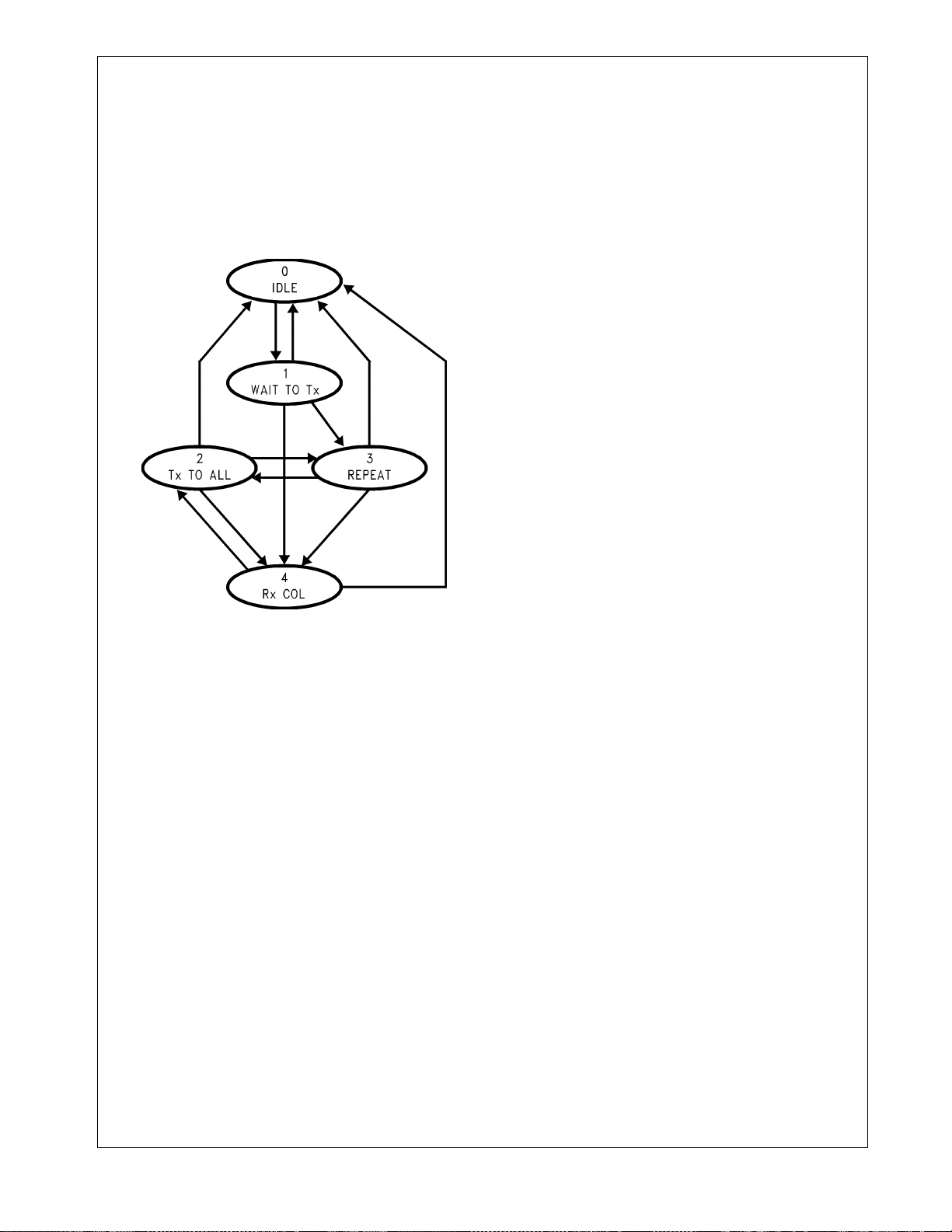
Figure 3 shows the Inter-RIC Bus State Diagram and Figure 4 shows the IEEE State Diagram.
Figure 3. Inter-RIC bus State Diag ram
15 www.national.com
Page 16
4.0 Functional Description
(Continued)
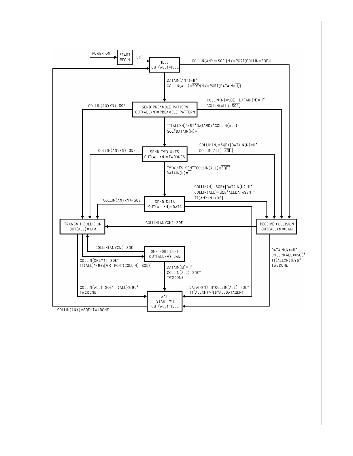
Figure 4. IEEE Repeater Main State Diagram
16 www.national.com
Page 17

4.0 Functional Description
(Continued)
The Port State Machine (PSM)
The two primary functions of t he PSM are to:
1. Control the transmission of repeated data, pseudo random data, and jam signal s over the attached segments .
2. Determine if a port will be the source of data or collision
informati on to be repe ated over t he network. This repeater port i s known as
quired to enable the repeater to transition from an
state to the
COLLISION
to locate the port that will be
packet.The dat a recei ved f ro m
PLL decoder and transmitted over the Inter-RIC bus. If a
collision occurs, the repeater enters the
COLLISION
tion is performed in order to determine which port is
PORT M. PORT M
other ports if the repeater enters the
state. In this state
ment. At that time, all other ports are still required to
transmit to t heir segments.
PORT N
SEND PREAMBLE PATTERN
states. (See Figure 4) This process is used
state. Then a subsequent arbitration opera-
is differentiated from the repeater’s
PORT M
. An arbit rati on proc ess is r e-
IDLE
or
RECEIVE
PORT N
for that particular
PORT N
is direct ed t o t he
TRANSMIT
ONE PORT LEFT
does not transmit to its seg-
The Main State Machine (MSM)
The MSM controls the operation of the shared f unct ional
blocks in each RIC2A as shown in the block diagram,
Figure 1, and performs the majority of the data and collision operations as defined by the IEEE specification.
Inter-RIC Bus (IRB) Operation
Overview
The IRB consists of eight signals. These signals implem ent
a protocol that may be used to connect multiple RIC2As
together. In this configuration, the logical function of a single repeater is maintained. The resulting multi- RIC2A
repeater syst em is compliant with the IEEE 802.3 Repeater
Specification and may even encompass several hundred
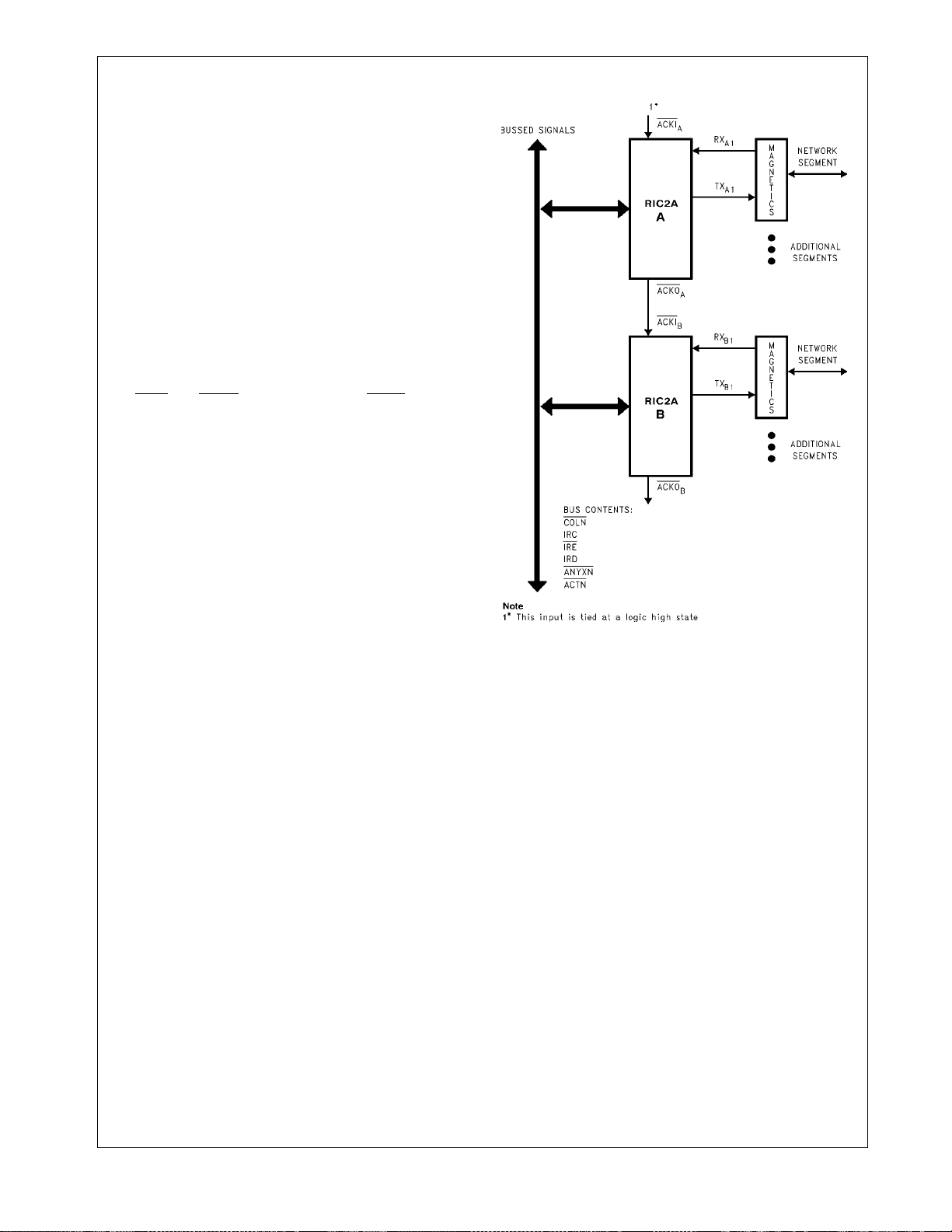
network segments. Figure 5 shows an example of a multiport RIC2A system.
Function Action
Preamble
Regeneration
Fragment
Extension
Elasticity Buffer
Control
Jam / Preamble
Pattern Generation
Transmit
Collision
Enforcement
Data Encoding
Control
Tw1
Enforcement
Tw2
Enforcement
Restore the length of the preamble pattern to the defined size.
Extend received dat a or col lision fragments to meet the minimum fragment
length of 96 bits.
A portion of the received pac ket may require storage in an Elasticity Buffer to
accommodate preamble regeneration.
In cases of receive or transmit collisions, a RIC2A is req uired t o t ransmit a
jam pattern (1010...).
Note: This pattern is the same as that used for preamble regeneration.
The
TRANSMIT COLLISION
quires a repeater to r emai n in this sta te
for at least 96 bit ti m es.
NRZ formatted data in the ela sticity
buffer must be encoded i nto Manchester formatted data pri or to re-transmission.
Enforce the Transmi t Recovery Time
specification.
Enforce Carrier Recovery Time specification on all ports with active collisi ons.
state re-
The interaction of the main and port state machines is visible, i n part, through the Inter-RIC bus.
17 www.national.com
Page 18

4.0 Functional Description
(Continued)
The IRB connects multiple RIC2As to realize the following
operations:
Port N
Identification (which port the repeater receives
data from)
Port M
Identification (which port last experienced a colli-
sion)
Data Transfer
RECEIVE COLLISION
identification
TRANSMIT COLLISION
DISABLE OUTPUT
identification
(jabber protection)
The following table briefly describes the operation of the
Inter-RIC bus signals, the conditions required for a RIC2A
to assert a signal, and which RIC2As (in a multi-RIC2A
system) would monitor the signal.
Inter-RIC
Bus Signal
Function
ACKI Input signal to Th e PSM arbit rati on
chain. This chain is employed to
identify
Note: A RIC2A whic h contains
PORT M
nal being low when its
PORT N
may be identified by its
and
ACKI
PORT M
input is high.
PORT N
ACKO
ACKO Output signal from the PSM arbi-
tration chain.
ACTN This sig nal denotes there i s activity
on
PORT N
or
PORT M.
ANYXN This signal denotes that a repeater
port that is not
PORT N
or
PORT M
is experiencing a collision.
COLN Denotes
PORT N
or
PORT M
periencing a collision.
IRE This signal ac ts as an act ivi ty fra m-
ing signal for the IRC and IRD signals.
Conditions Required for a RIC2A
to Drive this Signal
RIC2A Receiving the Signal
Not applicable This is depende nt upon the
method used to casca de
.
or
sig-
If this RIC2A contains port N, then
the device will assert this signal.
RIC2As , desc r ib ed in a follo w ing section.
This is dependent upon the
method used to casca de
RIC2As , desc r ib ed in a follo w ing section.
A RIC2A must contain
PORT M.
Note: Although this signal n ormally has only
one source asserting the signal active it is used
in a wired-or configuration.
Any RIC2A which satisfies the a bove
condition.
Note: This bus line is used in a wired-or configuration.
is ex-
A RIC2A must contain
PORT M.
PORT N
PORT N
or
The signal is monitored by all
RIC2As in the re peater syst em.
The signal is monitored by all
RIC2As in the re peater syst em.
or
The signal is monitored by all
other RIC2As in the repeater
system.
A RIC2A must contain
PORT N.
The signal is monitored by all
other RIC2As in the repeater
system.
IRD Decoded ser ial data, in NRZ for-
mat, received from the net work
segment attached to
PORT N.
IRC Clock signal associated with IRD
and IRE.
A RIC2A must contain
A RIC2A must contain
18 www.national.com
PORT N.
PORT N.
The signal is monitored by all
other RIC2As in the repeater
system.
The signal is monitored by all
other RIC2As in the repeater
system.
Page 19

4.0 Functional Description
Methods of RIC2A Cascading
In order to build multi-RIC2A repeaters,
PORT M
RIC2As in the system. Inside each RIC2A, the PSMs are
arranged in a logical arbitration chain where port 1 is the
highest and port 13 the lowest. The top of the chain, the
input to port 1 is accessible to the user via the RIC2A's
ACKI
becomes the ACKO
PORT N
chain with receive or collision activity.
is performed when the repeater is in the
M
when the repeater leaves the
state. In order for the arbitration chain to function, all that
needs to be done is to tie the ACKI
state. In multi-RIC2A systems there are two methods to
propagate the arbitration chain between RIC2As:
The first and most straight forward is to extend the arbitration chain by daisy chaining the ACKI
between RIC2As. In this approach one RIC2A is placed at
the top of the chain (its ACKI
ACKO
the next RIC2A and so on. This arrangement is simple to
implement but it places some topological restrictions upon
the repeater system. In particular, if the repeater is constructed using a backplane with removable pr inted circuit
boards. (These boards contain the RIC2As and their associated components.) If one of the boards is removed then
the ACKI
not operate cor rectly.
The second method of
this problem. This second technique relies on an external
parallel arbiter which monitors all o f the RIC2As' ACKO
nals and responds to the RIC2A with the highest priority. In
this scheme each RIC2A is assigned with a priority level.
One method of doing this is to assign a priority number
which reflects the position of a RIC2A board on the
repeater backplane, i.e., its slot number. When a RIC2A
experiences receive activity and the repeater system is in
the
nal arbitration logic drives the identifi cation number onto an
arbitration bus and the RIC2A containing
identified. An identical proced ure is used in the
COLLISION
not subject to the problems caused by missing boards, i.e.,
empty slots in the backplane. The logic associated with
asserting this arbi tration v ector in the v ario us packet repetition scenarios could be implemented in PAL® or GAL®
type devices.
Both of the above methods employ the same signals:
ACKI
tion.
The Inter-RIC bus allows mul ti -RIC2A operations to be performed in exactly the same manner as if there is only a single RIC2A in the system. The simplest way to describe the
operation of Inter-RIC bus is to see how it is used in a number of common packet repetition scenarios.
identification must be performed across all the
input pin. The output from the bottom of the chain
output pin. In a single RIC2A system
is defined as the highest port in the arbitration
is defined as the highest port in the chain with a collision
input is tied high), then the
signal from this RIC2A is sent to the ACKI input of
ACK O chain will be br oken and th e repeater will
PORT N or M
IDLE
state, the RIC2A board will assert ACKO. Exter-
state to identify
, ACKO and ACTN to perform
PORT M.
(Continued)
Por t N
IDLE
PORT N
identification
state.
and
PORT
TRANSMIT COLLISION
signal to a logic high
ACKO signals
identification avoids
sig-
PORT N
will be
TRANSMIT
Parallel arbitration is
PORT N
or M arbitra-
4.4 Examples Of Packet Repetition Scenarios
The operation of RIC2A is described b y the f oll owi ng e xamples of packet repetition scena rios.
Data Repetition Overview
When a packet is received at one port, the RIC2A checks
the source, and destination addresses of the packet. The
port configuration causes either a pseudo random bit
sequence, or the received packet to be transmi tt ed to diff erent ports.
If there is a destination address mismatch (secure mode),
then the RIC2A will generate a random pattern from the
first bit of the data field to that port. The data remains intact
on the Inter-RIC bus so other cascaded repeaters could
compare the destinat ion address with their local CAMs.
On a valid source address mismatch (secure mode),
RIC2A shall switch to random pattern both on the local
transmitt ing ports and the Inter-RIC bus.
Collision Scenari os Overview
The RIC 2A will adhere to all c ollision scenarios. When a
collisi on occ urs, RIC2A w ill switch to a jam patte r n to com ply with IEEE repeater specifications.
FIFO Condition Overview
Elasticity buffer error (ELBER) or FIFO overflow burst is
another condition that could take place anytime during the
packet transmission. The sequence of events for FIFO
burst is the same as those for collisi on.
Data Repetition Process
The first task to be performed is
This is an arbitration process performed by the Port State
Machines in the system. In situations where two or more
ports simultaneously receive packets, the Inter-RIC bus
operates by choosing one of the active ports, and forcing
the others to transmit data (real data or pseudo random
data). This is done in accordance with the IEEE specification's allowed exit paths from the
SEND PREAMBLE PATTERN
states.
The packet begins with a preamble pattern derived from
the RIC2A's on chip jam/preamble generator. The data
received at
plexor to the PLL decoder. Once phase lock has been
achieved, the decoded data (in NRZ f ormat) with its associated clock and enable signals, is asserted onto the IRD,
IRC, and IRE of the Inter-RIC bus. This serial data stream
is received from the bus by all RIC2As in the repeater and
directed to their elasticity buffers. Logic circuits monitor the
data stream and look for the Start of Frame Delimiter
(SFD). When it has been detected, data is loaded into the
elasticity buffer for later transmission. This will occur when
sufficient preamble has been transmitted and certain internal state machine oper ations have been fulfilled.
PORT N
is directed t hrough the receive multi-
PORT N
IDLE
or
RECEIVE COLLISION
identification.
state, i.e., to the
19 www.national.com
Page 20
4.0 Functional Description
Figure 5 shows two RIC2As A and B, daisy chained
together with RIC2A-A positioned at the top of the chain. If
a packet is received at port B1 of RIC2A-B, and then
repeated to the other ports in the system (non-secure
mode). Figure 6 shows the functional timing diagram for
the packet repetition si gnals. In this example only two ports
in the system are shown. In non-secure mode, the other
ports also repeat the packet. It also indicates the operation
of the RIC2As' st ate machines in so far as can be seen by
observing the Inter-RIC bus. For reference, the repeater's
state transitions are shown in terms of the states defined
by the IEEE specification. The location of
shown. The following section describes the repeater and
Inter-RIC bus transitions sho wn in Fi gure 6.
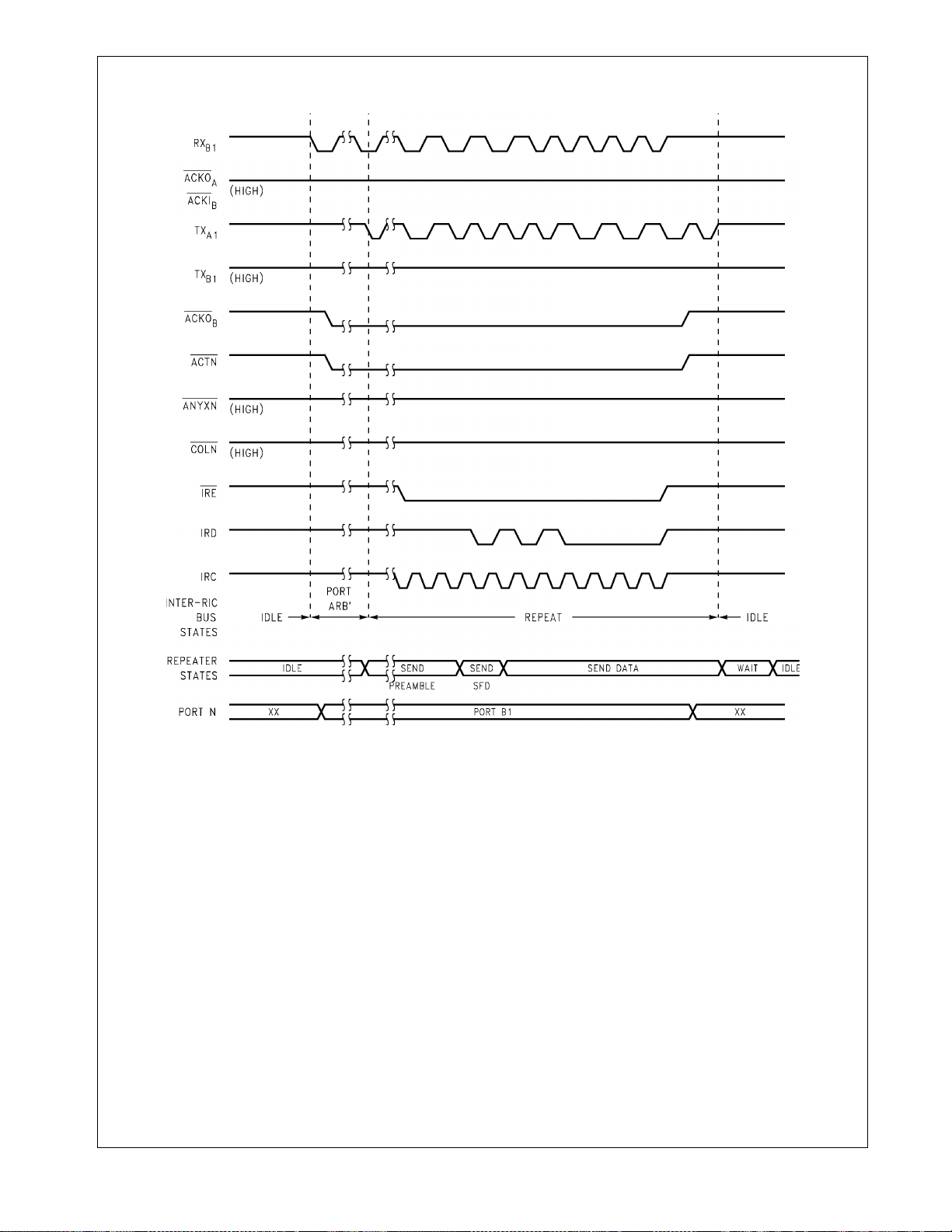
The repeater activity is stimulated by the data signal
received by port B1. The RIC2As in the system are alerted
to forthcoming repeater operation by the falling edges on
the ACKI
Following a defined start up delay the repeater moves to
the
the start up delay to perform port arbitration. When packet
transmission begins, the RIC2A system enters the
REPEAT state. The expected, for normal packet repetition,
sequence of repeater states,
SFD
the Inter-RIC bus. They are then merged into a single
REPEAT state. Similarly, the
as a combin ed Inte r-RI C bus I D L E stat e.
Once a REPEAT operation has begun (e.g. the repeater
leaves the
bits of data or jam/preamble onto its network segments. If
the duration of the received signal from
than 96 bits, the r epeater transitions to the
LISION
fragment extension.
After the packet data has been repeated, including the
emptying of the RIC2As' elasticity buffers, the RIC2A performs the
formed during the
diagram.
and ACKO daisy chain and the ACTN bus signal.
SEND PREAMBLE
and
SEND DATA
state. The RIC2A system utilizes
are followed, but are not visible at
WAIT
IDLE
state), it is required to transmit at least 96
state (described later). This behavior is known as
Tw 1
transmit recovery operation. This is per-
WAIT
state shown in the repeater state
(Continued)
PORT N
is also
SEND PREAMBLE, SEND
and
IDLE
states appear
PORT N
is shorter
RECE IVE COL -
Figure 5. RIC2A System Topology
20 www.national.com
Page 21
4.0 Functional Description
(Continued)
Note:
The activity shown on RX A1 represents the transmitted signal on TX A1 after being looped back by the attached transceiver.
1*
Figure 6. Data Repetition
21 www.national.com
Page 22
4.0 Functional Description
(Continued)
Note: 1 SEND PREAMBLE, SEND SFD, SEND DATA
AUI port shown.
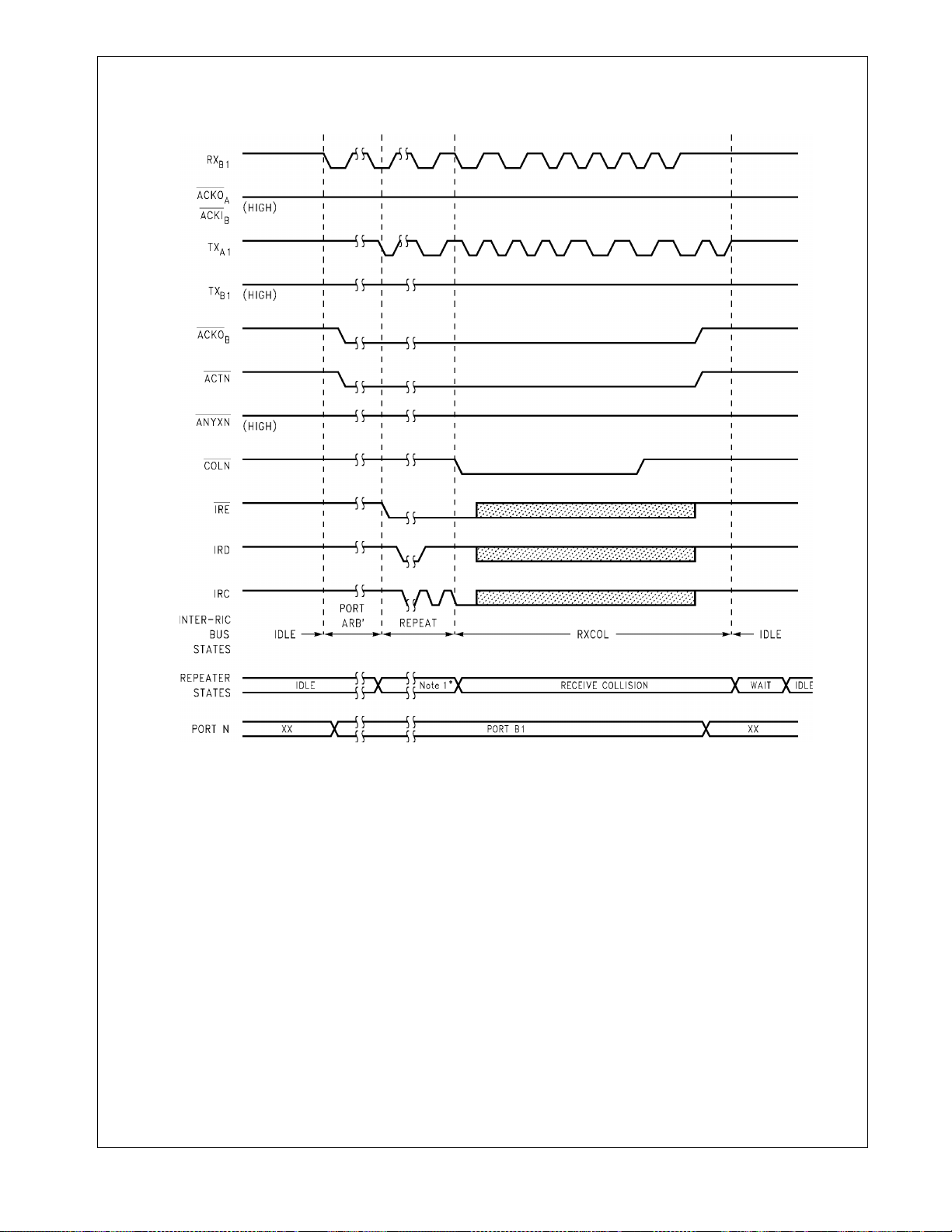
Figure 7. Receive Collision
22 www.national.com
Page 23

4.0 Functional Description
(Continued)
Receive Collisions (AUI Port only)
A receive collision is a collision which occurs on the network segment attached to the AUI port.
"receiv ed" in a similar manner as a data packet is received,
and then repeated to the other network segments. Not surprisingly, the receive collision propagation follows a similar
sequence of operations as data repetit ion.
An arbitration process is performed to find
preamble/jam pattern is transmitted by the repeater's other
ports. When the AUI port as
its segment the COLN
This forces all the RIC2As in the system to transmit a preamble/jam pattern to their segments. This is important
since they may be a lr eady transmitt ing data from their elasticity buffers. The repeater moves to the
SION
state and begins to transmit the jam pattern. The
repeater remains in this state until both the following conditions have been fulfill ed:
1. at least 96 bits have been transmitted onto the network,
2. the activity has ended.
Under close exami natio n, the repeate r specif ication reveals
that the actual end of activity has its own permutations of
conditions:
1. collision and receive data signals may end simulta-
neously,
2. receive data may appear t o end before co lli sion si gnals,
3. receive data may continue for some time after the end o f
the collision signal.
Network segments using coaxial media may experience
spurious gaps in segment activity when the collision signal
goes inactive. This arises from the inter-action between the
receive and collision signal squelch circuits, implemented
in coaxial transceivers, and the properties of the coaxial
cable itself. The repeater specification avoids propagation
of these activity gaps by extending collision activity by the
Tw2
wait time. Jam pattern transmission must be sustai ned
throughout this period. After this, the repeater will move to
the
WAIT
state unless there is a data signal being r eceived
by the AUI port as
The functional timing diagram, Figure 7, shows the opera-
tion of a repeater system during a receive collision. The
system configuration is the same as earlier described and
is shown in Figur e6.
The RIC2As perform the same
data repetition operations described previously. The system is noti fied of the receive collision on the AUI port by the
COLN
bus signal going active. This signal informs the main
state machines to send out the jam pattern rather than
valid data stored in the elasticity buffers. Once a collision
has occurred, the IRC, IRD and IRE
become undefined. When the collision has ended and the
Tw2
operation perfor med, the repeater moves to the
state.
PORT N.
PORT N
Inter-RIC bus signal is asserted.
PORT N
The collision is
PORT N
detects a collision on
and a
RECEIVE COLLI-
arbitration and
bus signals may
WAIT
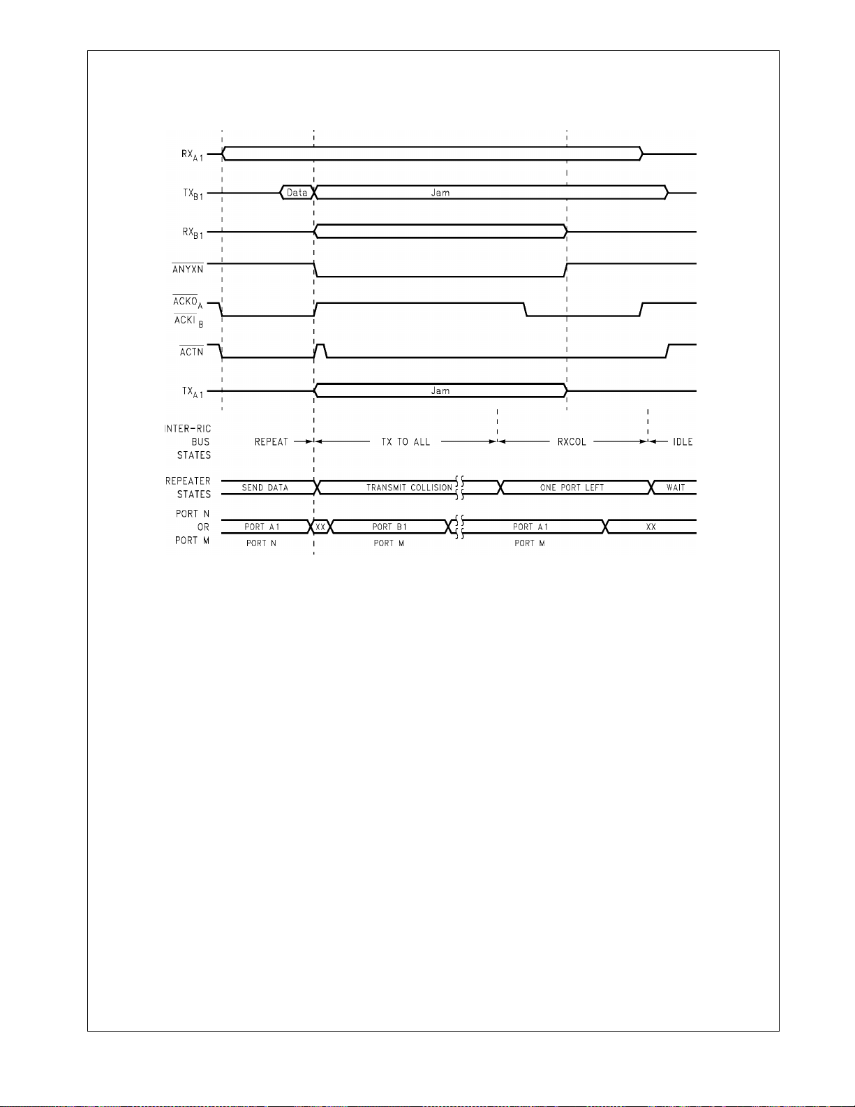
Transmit Collisions
A transmit collision is a collision that is detected upon a
segment to whi ch the repeater system is transmitting. The
port state machine monitoring the colliding segment
asserts the ANYXN
causes
to the
had been
encoded 1 on to its network segment. While i n the
PORT M
TRANSMIT COLLISION
PORT N
MIT COLLISION
mit the 1010... jam pattern, and
performed. Ea ch RIC2A is obligated, by the IEEE spec if ication, to ensure all of its ports transmit for at least 96 bits
once the
This tra n s mit activ ity is e nfor c ed by th e A N Y XN
While ANYXN
To ensure this situation lasts for at least 96 bits, the MSM
inside the RIC2As assert the ANYXN
period. After this period has elapsed, ANYXN
asserted if there are multiple ports with active collisions on
their network segments.
There are two possible ways for a repeater to leave the
TRANSMIT COLLISION
TRANSMIT COLLISION
when network activity, i.e., collisions and their
sions, end before the 96 bit enforced period expires. Under
these conditions the repeater system may move directly to
the
WAIT
state when 96 bits have been transmitted to all
ports. If the MSM enforced period ends and there is still
one port experiencing a collision, the
state is entered. This may be seen on the Inter-RIC bus
when ANYXN
ting to its network segment. In this circumstance the InterRIC bus transitions to the RECEIVE COLLISION state.
The repeater will remain in this state while
sion,
Tw2
collision extension and any receive signals are
present. When these conditions ar e not true, packet repetition finishes and the repeater enters the
Figure 8 shows a multi-RIC2A system operating under
transmit collision conditions. There are many different scenarios which may occur during a transmit collision, this figure illustrates one of these. The diagram begins with
packet reception by port A1. Port B1 experiences a collision, since it is not
the main state machines in the system to switch from data
to jam pattern transmission.
Port A1 is also monitoring the ANYXN
tion forces A1 to relinquish its
mitting, stop asserting ACTN
PSM arbitration signals (ACKO
it transmits will be a Manchester encoded "1" in the jam
pattern. Since port B1 is the only port with a collision, it
attains
does however assert ACTN
the PSM arbitratio n chain (forces ACKO
ensure that ANYXN
ports, including
After some time port A1 e xperiences a collision. This ari ses
from the presence of the packet being received from port
A1's segment and the jam signal the repeater is now transmitting onto this segment. Simultaneous receive and transmit activity on one segment results in a collision. Port A1
fulfills the same criteria as B1, i.e., it has an active collision
PORT M
bus signal. The assertion of ANYXN
arbitration to begin. The repeater moves
state when the port which
starts to transmit a Manchester
TRANS-
state, all ports of the repeater must trans-
PORT M
state has been entered.
is active, all R IC2A port s will transmit ja m.
signal through out this
state. The most straight forward is
arbitration is
bus signal.
will on ly be
Tw2
exten-
ONE PORT LEFT
is de-asserted and
PORT N
status and stops asserting ANYXN. It
stays active and thus force all of the
PORT M,
to transmit to their segm ents.
PORT M
it asserts ANYXN. This alerts
PORT N
and release its hold on the
A and ACKI B). The first bit
, and exer t its presence upon
stops transmit-
PORT M's
WAIT
state.
bus line. Its a sser-
status, start trans-
B low). The MSMs
colli-
23 www.national.com
Page 24

4.0 Functional Description
(Continued)
on its segment, but in addition it is higher in the arbitration
chain. This priority yields no benefits for port A1 since the
ANYXN
driving ANYXN
signal is still active. There are now two sources
, the MSMs and the collision on port B1.
Eventually the collision on port B1 ends and the ANYXN
extension by the MSMs expires. There is only one collision
on the network ( this may be deduced since ANYXN
tive) so the repeater will move to the
ONE PORT LEFT
is inac-
state. The RIC2A system treats this state in a similar manner to a receive collision with
PORT M
fulfillin g the role of
the receiving port. The difference from a true receive collision is that the switch from packet data to the jam pattern
has already been made (controlled by ANYXN
state of COLN
common with the operation of the
has no effect upon repeater operations. In
RECEIVE COLLISION
). Thus the
state, the repeater remains in this condition until the collision and receive activity on
repetition operation complete s when the
in the
WAIT
state has been perf ormed.
Note: In transmit collision conditions
which contained
during the
PORT N
TRANSMIT COLLISION
at the start of pac ket rep etition c ontai ns
PORT M
subside. The packet
Tw1
will only go active if the RIC2A
COLN
and
ONE PORT LEF T
recover y time
PORT M
states.
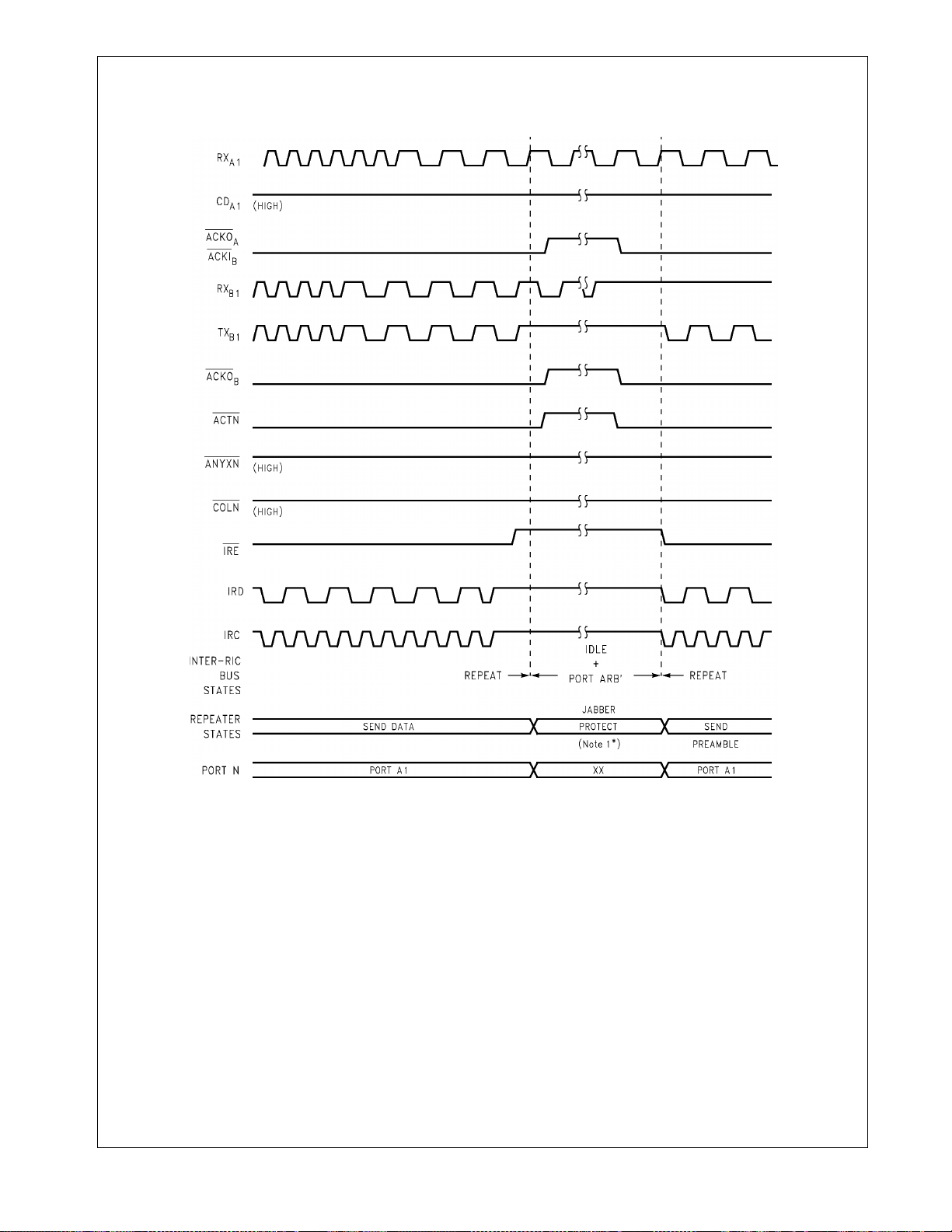
Jabber Protection
A repeater is required to disable transmit activity if the
length of its current transmission reaches the jabber protect limit. This is defined by the specification's
The repeater disables output for a time period defined by
the
Tw4
specification, after this period normal operation
may resum e.
Figure 9 shows the effect of a jabber length packet upon a
RIC2A based repeater system. The
state is entered from the
SEND DATA
JABBER PROTECT
state. While the
period is observed the Inter-RIC bus displays the IDLE
state. Thi s is misl eading si nce new pa ck et activi ty or co ntinuous activity (as shown in the diagram) does not result in
packet repetition. This may only occur when the
quirement has been sati sfied.
Tw3
Tw4
time.
Tw4
re-
24 www.national.com
Page 25
4.0 Functional Description
(Continued)
Note: The Inter-RIC bus is configured to use active low signals. AUI port shown
Figure 8. Transmit Colli sion
25 www.national.com
Page 26
4.0 Functional Description
(Continued)
Note:1* The IEEE Specificati on does not have a jabber protect s tate defined in i ts main state diagr am, this
behavior is defined in an additional MAU Jabber Lockup Protection state diagram.
Note: The Inter-RIC bus is configured to use active low signals. AUI port shown
Figure 9. Jabber Protect
26 www.national.com
Page 27
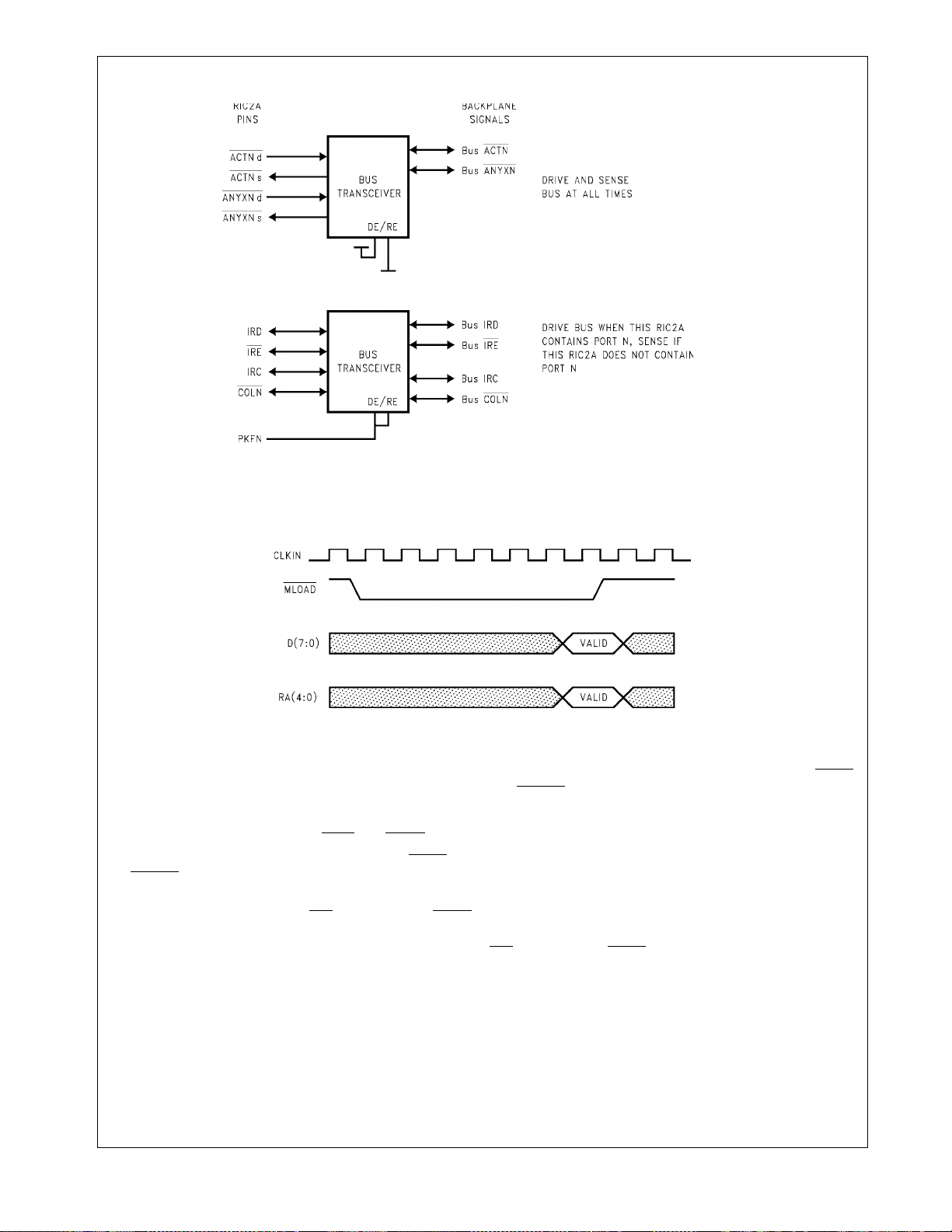
4.0 Functional Description
Note: DE = Bus Drive Enable active high, /RE = Bus Receive Enable active low
Note: The Inter-RIC bus is configured to use active low signals.
Figure 10. External Bus Trans ceiver Connection Diagram
(Continued)
Figure 11. Mode Load Operation
4.5 Description Of Hardware Connection For Inter-ric Bus
When considering the hardware interface, the Inter-RIC
bus may be viewed as consisting of three gr oups of signals:
1. Port Arbitration chain, namely: ACKI
2. Simultaneous drive and sense signals, i.e., ACTN
ANYXN
tiple devices).
3. Drive or sense signals, i.e., IRE
(Only one device ass erts these si gnals at any inst ance in
time).
The first set of signals are either used as point to point
links, or with external arbitration logic. In both cases the
load on these signals will not be large, so the on-chip drivers are adequate. This may not be true for signal classes
(2) and (3 ) .
The Inter-RIC bus has been designed to connect RIC2As
together di rectly, or via external bus transceiver s. The latter
is advantageous in large repeaters. In the second application the backplane is often heavily loaded and is beyond
. (Potenti ally these signals may be dr iven by mul-
and ACKO.
and
, IRD, IRC and COLN.
the drive capabilities of the on-chip bus drivers. The need
for simultaneous sense and drive capabilities on the ACTN
and ANYXN signals, and the desire to allow operation with
external bus transceivers, makes it necessary for the se bus
signals to each have a pair of pins on the RIC2A. One
drives the bus, the other senses the bus signal. When
external bus transceivers are used, they must be open collector / open drain to allow wire-ORing of the signals. Additionally, the drive and sense enables of the bus transceiver
should be tied in the acti ve state.
The uni-directional nature of information transfer on the
IRE
, IRD, IRC and COLN signals, means a RIC2A is either
driving these signals or receiving them from the bus, but
not both at the same time. Thus a single bi-directional
input / output pin is adequate for each of these signals. If
an external bus transceiver is used with these signals the
Packet Enable "PKEN" RIC2A output pin performs the
function of a drive enable and sense disable.
Figure 10 shows the RIC2A con nected to the Inter-RIC bus
via external bus transceivers, such as National's DS3893A
bus transceiv ers.
27 www.national.com
Page 28

4.0 Functional Description
Some bus transceivers are of the inverting type. To allow
the Inter-RIC bus to utilize these transceivers, the RIC2A
may be configured to invert the active states of the ACTN
ANYXN
high. Thus they become active low once more when
passed through an inverting bus driver. This is particularly
important for the ACTN
signals must be used in a wired-or configuration. Incorrect
signal polarity would make the bus unusable.
, COLN and IRE signals from active l ow to active
and ANYXN bus lines, since these
(Continued)
4.6 Processor and Display Interface
The processor interface pins, which include the data bus,
address bus and control signals, actually perform three
operations which are multiplexed on these pins. These
operations are:
1. The Mode Load Operation, which performs a power up
initialization cycle upon the RIC2A.
2. Display Update Cycles, which are refresh operations for
updating the di splay LEDs.
3. Processor Access Cycles, which allows µP’s to communicate with the RIC2A’s registers.
These three operations are described below.
Mode Load Operation
The Mode Load Operation is a hardware initialization procedure performed at power on. It loads vital device configuration information into on chip configuration registers. In
addition to its configuration function, the MLOAD
RIC2A's reset input. When MLOAD
RIC2A's repe ater timers, state machines, segment partition
logic and hub managem ent logic are reset.
The Mode Load Operation may be accomplished b y attaching the appropriate set of pull up and pull down resistors to
the data and register address pins to assert logic high or
low signals onto these pins, and then providing a rising
edge on the MLOAD
execution of this function not only requires both falling and
rising edges of MLOAD
out. The mapping of chip functions to the configuration
inputs is sho wn in Tab le1.
In a complex repeater system, the Mode Load Operation
may be performed using a processor write cycle. This
would require the MLOAD
CPU's write strobe via some decoding logic, and included
in the processor's memory map.
To support the security options, pin D0 of the data bus during MLOAD is assigned to co nfi gure RIC2A. A pull up (nonsecurity mode) or a pull down (security mode) on this pin
defines the desired security level . By using this bit, the user
could also take advantage of the learning mode, as
described below.
pin as is shown in Figure 11. Proper
, but also an active CLKIN through-
pin to be connected to the
is low, all of the
pin is the
Learning of Port Source Address(es)
Learning mode could be invoked in two ways according to
bit D0 of MLoad configuration. Only the port CAMs are
capable of l earning the addresses:
1. When D0=0, upon power up and by default, LME, SME,
ESA and EDA bits in the Port Security Configuration
Register (PSCR) are set globally. This means that each
port will lear n the address of the node c onnected to it by
the reception of the first good packet. The second ad-
,
dress is learned only if it is different from the first one.
Only the address of a valid length packet without FAE
(Frame Alignment Error) and/or CRC errors can be
learned. As soon as the address is l earned by any of th e
two CAM locations, RIC2A will set the corresponding
ADV (Address Valid) bit in Port CAM Pointer Register.
To start the address com parison, the SAC (Start Comparison) bit must be set (SAC=1) b y the u ser. RI C2A wil l
only use this CAM location for comparison when the
ADV bit is set (ADV=1), whether LME is 1 or 0. These
four bits in PSCR could be disabled later on a per port
basis, which allow all the packets regardle ss of t heir address to pass through the repeater.
2. When D0=1 for MLOAD, secur ity could still be done, but
this time it mea ns that the user s hould set t he LME, SME,
ESA and/or EDA bits in the Port Secu rity Configuration
Register. The rest of the operation is the same as when
D0 is equal to zero.
It is important to note that RIC2A will learn the address of
the packet if LME is set regardless of the D0 setting of
MLoad, i.e. secure or non-secure mode.
It is also very important to note that for proper address
learning, LME and SAC should not be set together.
When the repeater is in non-secure mode, then the comparison will not take place between the incoming address
and the learned address.
When the repeater is in secure mode, and the LME bit is
set, then the processor read/write access will be i gnored
for the port CAM entries. That is read/ write cycles are
completed, however unknown values are read during the
learning process. Data will not be written into the CAM
entries until the end of the learning process.
It may be desired not to randomize the outgoing data and
transmit the data intact when there is a valid source
address mismatch. The Generate Random Pattern bit,
GRP in the Global Security Register, will provide the
option.
If GRP is set (GRP=1) and there is a source address mismatch, then RIC2A will not generate random pattern; the
packet will be transmitted out and the Hub Manager will be
informed about th e source
For this option to work properly, GRP=ESA=1 and EDA=0.
If EDA is also set to 1, then the packet will be randomized
on ports with valid DA mismatches, and this functionality
will not work.
address mismatch.
28 www.national.com
Page 29

4.0 Functional Description
T able 1. Pin Definitions for Options in the Mode Load Operation
(Continued)
Pin
Name
D0 SCRTY Security
D1 TW2 5 bits 3 bits This allows the user to sel ect one of two values for the
D2 CCLIM 63 31 The partition specification requires a port to be partitioned
D3 LPPART Selected Not Selected The RIC2A may be configured to partition a port if the
Program-
ming
Function
Effect when
Bit is 0
Mode
Effect when
Bit is 1
Non-Security
Mode
Function
This bit configures RIC2A security feat ure options.
When D0 =0 LME, SME, ESA, EDA bits in the Port
Security Configuration Register (PSCR) are set gl obally.
When D0=1 security can still be done, but now th e user
needs to set the above bits in the PSCR register.
repeater speci fi cation TW2 time. The lo wer limit (3 bits)
meets the IEEE specification . The upper limit (5 bits ) is not
specification compliant but may provide users wit h higher
network throughpu t by avoidi ng spurious network activit y
gaps when using coaxial (10BASE2, 10BASE5) network
segments.
after a certain number of consecutive collisions. The
RIC2A has two values available to allow users to customize
the partitioning a lgorithm to t heir environment. Please ref er
to the Partition St ate Machine, in data sheet section 7.3.
segment transceiver does not loopback data to the port
when the port is transmitting to it, as described in the
Partition State Machine.
D4 OWCE Selected Not Selected This configuration bi t allows the o n-chip partition algorithm
to include out of window collisions into the collisions it
monitors, as described in the Partition State Machine.
D5 TXONLY Selected Not Selected This configuration bi t allows the o n-chip partition algorithm
to restrict segment reconnection, as described in the
Partition State Machine.
D6 DPART Selected Not Selected The Partition state machines for all ports may be disabled
by writing a logic z ero to this bit during the mode load
operation.
D7 MIN/MAX Minimum Mode Maximum Mode The operation of the display updat e block is controlled by
the value of t his configuration bi t, as described in the
Display Update Cycles section.
RA0 TP X X All ports (2 to 13) use the inte rnal 10BASE- T tr ansceivers.
(Internally configured)
RA1 TP X X
RA2 BINV Active High
Signals
RA3 EXPLL External PLL Internal PLL If desired, the RIC2A may be used wit h an external
RA4 resv Not Perm it te d Required To ensure correct devi ce operation, this bit must be writt en
Active Low Sig-
nals
This selection determines whether the Inter-RIC signals:
IRE, ACTN, ANYXN, COLN and Management bus signal
MCRS are active high or lo w.
decoder, this configuration bit performs the selection.
with a logic one during the mode lo ad operation.
29 www.national.com
Page 30

4.0 Functional Description
(Continued)
4.7 Description Of Hardware Connection For Processor And Display Interface
Display Update Cycles
The RIC2A possesses control logic and interface pins
which may be used to provide status information concerning activity on the attached network segments and the current status of repeater functions. These status cycles are
completely autonomous and require only simple support
circuitry to produce the data in a form suitable for a light
emitting diode "LED" display. The display may be used in
one of two modes:
1. Minimum mode - General Repeater Status LEDs
2. Maximum mode - Individual Port Status LEDs
Minimum mode, intended for simple LED displays, makes
available four status indicators. The first LED denotes
whether the RIC2A has been forced to activate its jabber
protect functions. The remaining 3 LEDs indicate if any of
the RIC2A's network segments are: (1) experiencing a collision, (2) receiving data, (3) currently partitioned. When
minimum display mode is selected the only external components required are a 74LS374 type latch, the LEDs and
their curr ent limiting resist ors.
Maximum mode differs from minimum mode by providing
displa y inf ormati on specif ic to individu al netw ork segments .
This information denotes the collision activity, packet
reception and partition status of each segment. In the case
of 10BASE-T segments t he link integrity s tat us and polarity
of the received data are also made available. The wide
variety of information available in maximum mode may be
used in its entirety or in part. This allows the system
designer to choose the appropriate complexity of status
display commensurate with the specification of the end
equipment.
The signals provided and their timing relationships have
been designed to interface directly with 74LS259 type
addressable latches. The number of latches used being
depend upon the complexity of the display. Since the
latches are octal, a pair is needed to display each type of
segment specific data (13 ports means 13 latch bits). The
accompanyi ng Tabl e2 and Table 3 show the function of the
interface pins in minimum and maximum modes. Table 4
shows the location of each port's status infor mation when
maximum mode is selected. This may be compared with
the connection diagram Figure 12.
Immediately following the Mode Load Operation (when the
MLOAD
logic performs an LED test operation. This operation lasts
one second. While it is in effect, all of the utilized LEDs will
blink on. Thus, an installation engineer is able to test the
operation of the display by forcing the RIC2A into a reset
cycle (MLOAD
pin starts the LED test cycle.
the RIC2A does not perform packet repetition operations.
The status display possesses a capability to lengthen the
time an LED is active. At the end of the repetition of a
packet, the display is frozen showing the current activity.
This freezin g lasts for 30 millisecon ds or until a subsequent
packe t is repeated. Thus at low levels of pack et activity, the
display stretches activity inform ation to make it discernible
to the human eye. At high traffic rates the relative brightness of the LEDs indicates those segments with high or
low activity.
It should be mentioned that when the Real Time Interrupt
(RTI) occurs, the display update cycle will stop and after
RTI is serviced, the display update cycle will resume activity.
pin transitions to a high logic state), the display
forced low). The rising edge on the MLOAD
Dur ing the LED t est cy cle
Table 2. Status Display Pin Functions in Minimum Mode
Signal Pin Name Function in MINIMUM MODE
D0 No operation
D1 Provides status information indicating if there is a collision occurring on one of the segments
attached to this RIC2A.
D2 Provides status inform ation indi catin g if one of t his RI C2A's por ts i s rece iving a data o r collisi on
D3 Provides status informat ion indicating that the RIC2A has experienced a jabber protect condi-
D4 Provides Status information indicating if one of the RIC2A's segments is partitioned.
D(7:5) No operation
STR0 This signal is the l atch enable for the 374 type latc h.
STR1 This signal is held at a logic one.
packet from a segment attached to this RIC2A.
tion.
30 www.national.com
Page 31

4.0 Functional Description
(Continued)
T able 3. Status Display Pin Functi ons in Maximum Mode
Signal Pin Name Function in MAXIMUM MODE
D0 Provides status inform ation concer ning the Link Int egrity status of 10BASE-T segment s. This si gnal
should be connected to t he data inputs of the chosen pair of 74LS259 latches.
D1 Provides status information indicating if there is a collision occurring on one of the segments at-
tached to this RIC2A. This signal should be connected to the data inputs of the chosen pair of
74LS259 latches.
D2 Provides status information indicating if one of thi s RIC2A' s ports is receiving a data or a collision
packet from its segment . This signal should be connected to the data inputs of the chosen pair of
74LS259 latches.
D3 Provides Status information indicating that th e RIC2A has experienced a jabber protec t condition.
Additionally it denot es which of its ports are partitione d. This signal should be connecte d to the data
inputs of the chosen pair of 74LS259 latches.
D4 Provides status inf ormation indica ti ng if one of this RIC2A's ports is receiving data of inverse polar-
ity. This status out put is only val id if the port is conf i gured to use its intern al 10BASE-T tr anscei ver.
The signal should be conne cted to the data inputs of the chos en pair of 74LS259 latches.
D(7:5) These signals provi de the repeater port address corresponding to the data available on D(4:0).
STR0 This signal is the latch enable for the lower byte latches, that is the 74LS259s which display infor-
mation concerning ports 1 to 7.
STR1 This signal is the latch enable for the upper byte latches, that is the 74LS259s which display infor-
mation concerning ports 8 to 13.
Table 4. Maximum Mode LED Definitions
74LS259 Latch Inputs =
STR0
259 Output Q0 Q1 Q2 Q3 Q4 Q5 Q6 Q7
259 Addr S2-0 000 001 010 011 100 101 110 111
RIC2A Port Number 1 (AUI) 2 3 4 5 6 7
RIC2A DO 259 #1 LINK LINK LINK LINK LINK LINK
RIC2A D1 259 # 2 ACOL COL COL COL COL COL COL COL
RIC2A D2 259 # 3 AREC REC REC REC REC REC REC REC
RIC2A D3 259 # 4 JAB PART PART PART PART PART PART PART
RIC2A D4 259 # 5 BDPOL BDPOL BDPOL BDPOL BDPOL BDPOL
74LS259 (or Equiv.) Latch Inputs =
STR0
259 Outputs Q0Q1Q2Q3Q4Q5Q6Q7
259 Addr S2-0 000 001 010 011 100 101 110 111
RIC2A Port Number 8 9 10 11 12 13
RIC2A DO 259 # 6 LINK LINK LINK LINK LINK LINK
RIC2A D1 259 # 7 COL COL COL COL COL COL
RIC2A D2 259 # 8 REC REC R EC REC REC REC
RIC2A D3 259 # 9 PART PART PART PART PART PART
RIC2A D4 259 # 10 BDPOL BDPOL BDPOL BDPOL BDPOL BDPOL
Note: ACOL= Any Port Collision, AREC= Any Po rt Reception, JAB= Any Port Jabbering, LINK=Port Link, CO L= Port Collision, REC=Por t Reception,
PART=Port Partitioned, BDPOL=Bad (inverse) Polarity of received data
This shows the LED Output Function s for the LED Dr iver s when 74LS259 s are used . The top table r efers to the bank of 4 74LS259s latched wi th
and the lower ta ble refer s to the bank of 4 7 4LS259s lat ched wi th
74LS259s then drive the LINK LEDs.
. For example the RIC2A' s D0 dat a signal g oes to 259 # 1 and #5. These two
STR0
STR0
,
31 www.national.com
Page 32

4.0 Functional Description
(Continued)
Figure 12. Maximum Mode LED Display (All Avai lable Status Bits Used)
32 www.national.com
Page 33

4.0 Functional Description
(Continued)
Figure 13. Processor Connecti on Diagram
33 www.national.com
Page 34

4.0 Functional Description
(Continued)
Processor Access Cycles
Access to the RIC2A's on- chip registers is made via its processor interface, which utilizes conventional non-multiplexed address (five bit) and data (eight bit) busses. Also,
the data bus provides data and address information to
external chip display latches during the display update
cycles. While performing these cycles, the RIC2A behaves
as a master of its data bus. Consequently a TRI-STATE bidirectional bus transceiver, e.g. 74LS245, must be placed
between the RIC2A and any processor.
The RIC2A provides a scheme to facilitate faster register
access. The Lower Event Information Register (Page 1H,
Address 1FH) has a Disable LED Update bit (DLU). The
setting of this bit causes the RIC2A to stop LED updates.
This schem e “unshares” the d ata bus, holding the RIC2A in
slave access mode. This mode reduces the maximum
read/write cycle time to approximately 400 ns.
The processor requests a register access by asserting the
read “RD
responds by completing any current display update cycle
and asserts the TRI-STATE buffer enable signal “BUFEN
If the pr ocessor cycle is a write cycle then the RIC2A's data
buffers are disabled to prevent contention problems. In
order to interface to the RIC2A in a processor controlled
system, a PAL device may be used to perform the following
operations:
1. To locate the RIC2A in the processor' s memory map (a d-
2. To generate the RIC2A's read and wri te strobes,
3. To control the directi on signal for the 74LS245.
An example of the processor and display interfaces is
shown in Figure13.
” or write “WR” input strobes. The RIC2A
dress decode),
Interrupt Handling
The DP83953 RIC2A offers an alternative method for a
faster access to determine the source of the Event Logg ing
Interrupt (ELI) register than the DP83950 RIC.
For an event logging interrupt due to flag found, the
DP83950 RIC
1. Read the Page Select Register (Address 10H) to locate
the source of Event Logging Interrupt.
2. Read all the Port Event Recording Registers (Page 1H,
Address 11H to 1DH) to find the port and the event responsible for Eve nt Logging Interrupt.
DP83953 RIC2A
The
sch eme for a fast er acc e ss:
1. Read Page Select Register (Address 10H) to locate the
source of Event Loggi ng Int errupt.
2. Read the Event Information Registers (Page 1H, addresses 1EH and 1FH) to locate the port responsible for
interrupt.
”.
3. Read the Event Recording register of that port to find
which specific event caused th e Eve nt Loggi ng Int errup t.
requires the following scheme:
allows the following alternate
34 www.national.com
Page 35

5.0 HUB MANAGEMENT SUPPORT
The RIC2A provides information regarding the status of its
ports and the packets being repeated. This data is available in three forms:
1. Counted Events - Network events accumulated into the
RIC2A's 16 bit Event Counter Registers.
2. Recorded Events - Network events that set bits in the
Event Record Registers.
3. Hub Management Status Packets- This is the information sent over the Management Bus in a serial format to
be decoded by an Ethernet Controller board.
The processor interface provides access to all counted and
recorded event information. This data is port specific and
may be used to generate interrupts via the Event Logging
Interr u pt “E L I
port, each repeater port has its own event record register
and event counter. The counters and event record re gisters
hav e user definable masks which enable them t o be configured to count and record a variety of events. The counters
and record registers are designed to be used together so
that detailed information (i.e., a count value) can be held
on-chip for a specific network cond it ion. More general information, i.e. the occurrence of certain types of events, may
be retained in on-chip latches. Thus, the u ser can configure
the counters to increment upon a rapidly occurring event
(most likely to be used to count collisions), and the record
registers m ay log the occurrence of less frequent error conditions such as jabber protect packets.
” pin. Since the information is specific to each
5.1 Event Cou nt i ng Fu nction
The counters may inc remen t upon the occurr ence of one of
the categories of event as desc ribed below.
Potential sources for Counter increment:
Jabber Protection (JAB):
the length of a received packet from its associated port
causes the repeater state machine to enter the jabber protect sta te.
Elasticity Buffer Error (ELBER):
ments if an Elasticity Buffer underf low or overflow condition
occurs during packet reception. This flag is held inactive if
a collision occurs during pack et reception or if a phase l ock
error, described below, has already occurred during packet
reception.
Phase Lock Error (PLER):
the phase lock loop decoder loses lock during packet
reception. Phase lock onto the received data stream may
or may not be recover ed later in the packet, so data errors
may have occurred. This flag is held inactive if a collision
occurs.
Non SFD Packet (NSFD):
start of frame delimiter (SFD) is not detected the port
counter will increment. NSFD counting is inhibited if the
pack et experiences a colli sion.
Out of Window Collision (OWC):
goes active when a port experiences a collision outside of
the network slot ti m e.
The port counter increments if
The port counter incre-
A phase lock error is caused if
If a packet is received and the
The OWC flag for a port
Transmit Collision (TXCOL):
when the repeater e xperiences a transmit collision.
Receive Collision (RXCOL):
goes active when the port is the receive source of network
activity and suffers a collision, provided no other network
segments experience collisions. At that point, the receive
collision fla g for the receiving port will be set.
Partition (PART):
port becomes partitioned.
Bad Link (BDLNK):
10BASE-T port has entered the link lost st ate.
Short Event reception (SE):
if the received packet is less than 74 bits long and no collision occurs during re ception.
Packet Recep tion (REC) :
port counter increments .
In order to utilize the counters the user must choose, from
the above list, the desired statistics for counting. This
counter mask information must be written to the appropriate registe rs (i.e. Upper and Lower Event Count Mask Registers). For the exact bit patterns of these registers please
read Section 7.0 of the data sheet.
If the counters are configured to count network collisions
and the ap propriate masks have been set, then whenever a
collision occurs on a segment, this information will be
latched by the hub management support logic. At the end
of repetition of the packet the collision status, respective to
each port, is loaded into that port's counter. This operation
is completely autonomous and requires no processor intervention.
Each counter is 16 bits long and may be directly read by
the processor. Additionally each counter has a number of
decodes to indicate the current value of the count. There
are three decodes:
low count (a va lue of 00FF Hex and under),
high count (a val ue of C000 Hex and above),
full count (a value of FFFF Hex).
The decodes from each counter are logically "ORed"
together and may be used as interrupts for the ELI
pin. Additionally, the status of these bits may be obser ved
by reading the Page Select Register. In order to enable
these threshold interrupts, the appropriate interrupt mask
bit must be written to the Management and Interrupt Configuration Register. See Section 7.0 for regi ster details.
In addition to their event masking functions, the Upper
Event Counting Mask Register (UECMR) possesses two
bits that control operation of the counters. The Reset On
Read “ROR” bit resets the counters after performing a processor read cycle. If this ROR bit is not set, which is used
to zero the counters, then the counters must be either written with zeros by the processor or allowed to rollover to all
zeros. The Freeze When Full “FWF” bit prevents counter
rollover by inhibiting count up cycles (these cycles happen
when chosen events occur), thereby fre ezing that particular
counter at FFFF Hex .
The port counter increments when a
The port counter increments when a
The TXCOL flag is enabled
The RXCOL flag for a port
The port counter increments
When a packet is received the
interrupt
35 www.national.com
Page 36

5.0 HUB MANAGEMENT SUPPORT
(Continued)
The port event counters may also be controlled by the
Counter Decrement (CDEC
) pin. As the name suggests, a
logic lo w state on this pin wil l decrement all the counters by
a single value. The pulses on CDEC
are internally synchronized and scheduled to avoid any conflict with the "up
counting" activity. If an “up count” and a “down count” occur
simultaneously, then the “down count” is delayed until the
“up count” has completed. This combination of up and
down counting capability enables the RIC2A's on-chip
counters to provide a simple rolling average, or be used as
extensions of larger external counters.
Note: If the FWF option is enabled then the count down operation is disabled
from those registers which have reac hed FFFF Hex and consequently have
been frozen. Thus, the FWF and
cation. A frozen counter indicates that a rate has gone out of bounds, due to
incrementing too fast or too slowly. If the low count and high count dec odes
are employed as eithe r interr upts or poll cy cles, th e direct ion of the r ate excursion may be determined.
bits will be set to provide rate indi-
CDEC
New Hub Management Counters
The are 13 m ore 8 bit coun ter s on the RIC2A tha n provided
on the DP83950 RIC. These counters will count events
specified in the Event Count and Interrupt Mask Register 2
(ECIMR2), such as Frame Check Sequence, Frame Alignment Error, Partition, Out of Window Collision. Also, this
register includes "Reset On Read" and "Freeze When Full"
control bits.
It should be noted that Counter Decrement (CDEC) will not
be used with the ECMR2. Also, no real time or event logging interrupt will be generated for this register.
Reading the Event Counters
The RIC2A's external data bus is eight bits wide. Since the
event counters are 16 bits long, two processor read cycles
are required to read the counter value. In order to ensure
correct counter values and simultaneously allow event
counts and processor accesses, values are stored in a
temporary holding register. A read cycle to either the
lower or upper byte of a counter causes both bytes to be
latched into the temporary holding register. Thus, when the
other byte of the count er is obtained, the temporary holding
register is accessed (not the actual counter register). This
ensures that the upper and lower bytes contain the value
sampled at the same instant in time.
There are no restrictions concerning whether the upper or
lower byte is read first. However, to ensure the "same
instance value" is obtained, the reads of the upper then
lower byte (or vice versa) should be performed as consecutive reads of the counter array. Other “non counter” registers may be read in between these read cycles and write
cycles may be performed. If another counter is read, or the
same byte of the original counter is read again, then the
holding register is updated from the counter array, and the
unre ad byte is l o st.
If the reset on read option is employed, then the counter is
reset after the transfer to the holding register is perform ed.
Processor read and write cycles are scheduled to avoid
conflict with count up or c ount down operations. In the case
of a processor read, the count value i s stable as i t is loaded
into the holding register. In the case of a processor write,
the newly written value is stable enough to be incremented
or decremented by any subsequent count operation. During the period of time when the MLOAD
pin is low, (power
on reset) all counters are reset to zero and all count masks
are forced into the disabled state. Section 7.0 of the data
sheet details the address location of the port event
counters.
5.2 Event Record Function
As stated previously, each repeater port has its own 8 bit
Event Recording status register. Each bit may be dedicated
to log the occurrence of a particular event (see Section 7.0
for detailed description ). The Event Recording Mask Register controls the logging of these events. Additionally, the
particular mask bi t must be set to record an event. Similar
to the scheme employed for the event counters, the
recorded events are latched during the repetition of a
packet then automatically loaded into the recording registers at the end of packet transmission. When one of the
unmasked events occurs, that particular port register bit is
set. The regi ster bits for all of the ports are logicall y "ORed"
together to produce a Flag Found "FF" signal. The Page
Select Register contains the Flag Found indicator. Additionally, if the appropriate mask bit is enabled in the Management and Interrupt Configuration Register then an
interrupt may be generated
A processor read cycle to an Event Record Register resets
any bits set in that register. Read operations are scheduled
to guarantee that data does not change during the cycle.
Any internal bit setting event that immediately follows a processor read will be successful. Events that may be
recorded are described below:
Jabber Protection (JAB):
length of a received packet causes the repeater state
machine to enter into the Jabber Protect state.
Elasticity Buffer Error (ELBER):
buffer underflow or overflow condition occurs during packet
reception. The flag is held inactive if a collision occurs during packet reception or if a phase lock error has already
occurred during pac ket reception .
Phase Lock Error (PLER):
the phase lock loop decoder loses lock during packet
reception. A phase lock onto the received data stream may
not be recoverable later in the packet and dat a errors may
have occurred. This flag is held inactive if a collision
occurs.
Non SFD Packet (NSFD):
start of frame delimiter (SFD) is not detected, this flag will
go active. The flag is held inactive if a collision occurs during packet reception.
Out of Window Collision (OWC):
sion flag goes active when a port experiences a collision
outside of the netw ork slot time.
Partition (PART):
This flag goes active when a port
becomes partitioned.
Bad Link (BDLNK):
T port has entered the link lost stat e.
This flag goes active if the
This goes active if a
A phase lock error is caused if
If a packet is received and the
The out of window colli-
This flag goes active when a 10Base-
36 www.national.com
Page 37

5.0 HUB MANAGEMENT SUPPORT
Short Event reception (SE):
This flag goes active if the
(Continued)
received packet is less than 74 bits long and no collision
occurs during rece pti on.
5.3 Management Interface Operation
The Hub Management interface provides a mechanism to
combine repeater status information with packet information to for m a hub management packet. A serial bus interface consisting of carrier sense, receive clock and receive
data is designed to connect one or more RIC2A's over a
backplane bus to another device, such as the DP83932
“SONIC
TM
” controller. The SONIC combined with the
RIC2As form a powerful entity for network statistics gathering.
The management interface consists of four pins:
MRXC
MCRS
MRXD
PCOMP
Management Receive Clock - 10MHz NRZ
Clock output.
Management Carrier Sense - Input/ Output
indicating of valid data stream.
Management Receive Data - NRZ Data output
synchronous to MRXC
Packet Compress - Input to truncate the
packe t' s data field.
The first three signals will emulat e the interface between an
Ethernet controller and a phase locked loop decoder (such
as the DP83932 SONIC and the DP83910 SNI) . These signals are driven by the RIC2A that receives the packet. The
MRXC and MRXD are comprised of a NRZ serial data
stream compatible with the DP83932. The PCOMP
signal
is driven by logic circuitry on the processor board. The
actual data stream transferred as MRXD is derived from
the transferred data (IRD) on the Inter-RIC bus. The difference between these two data streams are:
1. At the end of packe t repe tit ion a h ub man agement stat us
field is appended to the data stream. This status field,
consistin g of 7 bytes, is shown in Table 6, and Figure 14.
The information is obtained from several packet status
registers , which are describe d below. In accordance wit h
the IEEE Speci ficat ion t he leas t sign ifi cant bi t of a byt e is
transm itted first.
2. While the data of the repeated packet is being trans-
ferred over the m anageme nt bus, t he recei ved cloc k signals on the MRXC pin may be inhibi ted. This is contro lled
by the Packet Compress pin PCOMP
. If PC OM P is a sserted duri ng rep etit ion of t he packet then MR XC signal s
are inhibite d when the nu mber of bytes (after SFD) t ransferred over the m anageme nt bus equal s the num ber dis played in the Packet Compress Decode Register. This
register provides a means to delay the effect of the
PCOMP
signal, which may be generated early in the
packet's repetition. The packet compression feature reduces the amount of memory required to buffer packets
as they are received and are waitin g to be processed by
hub management software. In this application, an address dec oder, which forms part of the packet compress
logic, would monitor the address fields as they are received over the management bus. If the destination ad-
dress is not the address of the management node inside
the hub, then pac ket compr ess ion cou ld be e mploy ed. In
this manner only the port ion of t he pack et meaningf ul for
hub management interrogation (i.e., the address fields,)
is transferred to the SONIC and buf fered into memory.
If the repeated packet ends before PCOMP
is asserted
or before the required number of bytes have been transferred, then t he hub management status field is directly
appended to the r eceived data at a byt e bou ndary. If the
repeated packet is significantly longer than the value in
the Decode Register requires, and PCOMP
is asserted,
the status fields will be delayed until the end of pac ket
repetition. During this delay period MRXC clocks are inhibited, but the MCRS signal remains asserted.
Note: If
PCOMP
bytes defined by the packet compression register, then packet compression
will not occur.
is asserted late in the packet, i.e. , after the number of
The Management Interface may be fine tuned to meet the
timing considerations of the SONIC and the access time of
its associated packet memory. This refinement may be performed in two ways:
1. The default mode of oper ation of the Management interface is to only transfer packet s over the bus which have
a start of frame delimiter. Thus "packets" that are only
preamble/jam and do not convey any source or destination address information are inhibited. This filtering may
be disabled by wr iting a logi c zero to t he Management I nterface Configuration or "MIFCON" bit in the Management and Interrupt Configuration Register. See
Section 7.0 for details.
2. The Management bus has been designed to accommodate situations of maximum network utilization, for example, when collision generated fragments occur. (These
collision fragments may violate the IEEE 802.3 IFG
specificatio n.) The IFG required by the SONIC is a function of the time taken to release space in the receive
FIFO and to per form end of pac ket pr oces sing ( writ e status information i nto memory). These functi ons are primarily memory operations and consequently depend upon
bus latency and the memory access time of the system.
In order to allow the system designer some discretion in
choosing the speed of this memory, the RIC2A may be
configured to protect the SONIC from a potential FIFO
overflow condition. This is performed by utilizing the InterFrame Gap (IFG) Threshold Select Register.
The value (pl us one) hel d in this r egiste r def ines t he minimum allowable InterFrame Gap on the management
bus, measured in network bit times. If the gap is smaller
than this number, MCRS
is asserted but MXRC clocks
are inhibited. Consequently, no data is transferred. So,
the system designe r may decide wheth er or not to gat her
statistics or to monitor a subset on all packets, even
though they only occur wit h very small IFGs.
The status field, shown in Table 6, contains information of
six diff erent types. They are contained in seven Packet Status Registers "PSRs":
1. The RIC2A and port address fi elds [PSR(0) and (1)] ca n
uniquely identify the repeater port receiving the packet
out of a potential maximum of 832 ports sharing the
same management bus (64 RIC2As each with 13 ports).
37 www.national.com
Page 38

5.0 HUB MANAGEMENT SUPPORT
Thus all of the other status fields can be correctly attributed to the relevant port.
2. The status flags that the RIC2A produces for the event
counters or recording latches are supplied with each
packet [PSR( 2)]. Addit ional ly, the clean recei ve CLN st atus is supplied to allow the user to determine the re li ability of the address fields in the packet. The CLN status bit
[PSR(1)] is set if no collisions are experienced during the
repetition of the address fields.
3. The RIC2A has an on-chip timer to indicate when, relative to th e start of pack et repe titi on, a c olli sion, if any , occurred [PSR(3 )]. There is also a timer that indicates how
many bit times of IFG were seen on the net work between
repetition of this packet and the preceding one. This is
provided by [PSR(6)].
4. If packet compression is employed, the receive byte
count contained in the SONIC's packet descr iptor will i ndicate the n umber o f byte s trans ferre d over t he manag ement bus rather than the number of bytes in the packet.
For this reason the RIC2A that receives the packet
counts the number of received bytes and transfers this
over the management bus [PSR(4),(5)].
5. Appending a status field to a data packet will obviously
result in a CRC error being flagged by the SONIC. For
this reason, the RIC2A monitors the repeated data
stream to check for CRC and FAE errors. In the case of
FAE errors, the RIC2A provides additional dummy data
bits so tha t the status fields are always by te aligned. For
packets of non-valid length the CRC and FAE error bits
are not set. Refer to Table 5 for a complete description
(Continued)
of actions relating packet length to the setting of the Jab
and CRC bits, and learn functions.
6. As a final check upon the effectiveness of the management interface , the RIC2A tra nsf ers a bus spec ifi c status
bit to the SONIC. This flag Packet Compress Done
PCOMPD [PSR(0)], may be monitored by hub management software to check if the packet compression operation is enabled.
Figure 15 shows an example of a packet being transmitted
over the management bus. The first section of the diagram
(moving from left to right ) shows a s hort pre amble and SFD
pattern. The second region contains the packet's address
and the start of the data fields. At this time, logic on the
processor/SONIC card would determine if pac ket compression should be used on this packet. If the PCOMP
asserted, then packet transfer will stop when the number of
bytes transmitted equals the value defined in the decode
register. Hence, the MRXC signal is idle for the remainder
of the packet's data and CRC fiel ds. The final region shows
the transf er of the RIC2A's seven bytes of packet status .
The following pages describe the Hub Management registers that constit ute the management status field.
Note that Packet Status Register 5 (PSR5) can be configured to remain identical in the RIC2A as in the RIC, or
PSR5 can be modified to include the RUNT and SAM
(source address mismatch) information. PSR5 register bit
allocation is determined by the value of bit D2, MPS (Modify Packet Status), in the Global Security Register. When
the MPS bit is set, PSR5 register is modified.
signal is
Table 5. Relation of Packet Length to Jab Bit, CRCER bit and Learn
Pack et Length
Length< Min. size packet without CRC error no no no
Length<Min siz e packet with CRC error no no no
V alid length packet w/o CRC error no no yes
V alid length packet with CRC error no yes no
Max size<lengt h<Jab size without CRC error no no no
Max size< length<Jab size with CRC error no no no
Jab size packet without CRC error yes no no
Jab size packet with CRC error yes no no
Jab Bit (D2) of
PSR2 Register
CRCER Bit (D7)
of PSR1 Register
Learn
38 www.national.com
Page 39

5.0 HUB MANAGEMENT SUPPORT
Table 6. Hub Management Status Field
(Continued)
Packet status Register
PSR
D7 D6 D5 D4 D3 D2 D1 D0
PSR(0) A5 A4 A3 A2 A1 A0 PCOMPD resv
PSR(1) CRCER FAE COL CLN PA3 PA2 PA1 PA0
PSR(2) SE OWC NSFD PLER ELBER JAB CBT9 CBT8
PSR(3)
Collision Bit Timer
PSR(4)
Lower Repeat Byte Coun t
CBT7 CBT6 CBT5 CBT4 CBT3 CBT2 CBT1 CBT0
RBY7 RBY6 RBY5 RBY4 RBY3 RBY2 RBY1 RBY0
Note 2
PSR(5)
Upper Repeat Byte Count
PSR(6)
Inter Frame Gap Bit Timer
Note 1: T hese registers may only be reliably accessed via the management interface. Due to the nature of these registers they may not be accessed (read
or write cycles) via the processor interface.
Note 2: When MPS (Modify Packet Status) bit in the Global Security Register is:
MPS=0, Do not modify Packet Status Register 5. The RIC2A PSR5 is the same as the RIC PSR5.
MPS=1, The PSR5 register is modified in the RIC2A.
MPS=0
---------MPS=1
RBY15
-----------resv
RBY14
----------resv
RBY13
----------resv
RBY12
----------SAM
RBY11
----------RUNT
RBY10
----------RBY10
RBY9
---------RBY9
-----------
IBT7 IBT6 IBT5 IBT4 IBT3 IBT2 IBT1 IBT0
RBY8
RBY8
Figure 14.
Management Bus Packet Status Register TImin
39 www.national.com
g
Page 40

5.0 HUB MANAGEMENT SUPPORT
(Continued)
Figure 15.
Operation of the Management Bus
40 www.national.com
Page 41

5.0 HUB MANAGEMENT SUPPORT
(Continued)
Packet Status Register 0
D7 D6 D5 D4 D3 D2 D1 D0
A5 A4 A3 A2 A1 A0 PCOMPD resv
Bit Symbol Description
D0 resv
D1 PCOMPD
D(7:2) A(5:0)
Reserved for future use
Management software should not examine the state of this bit.
Packet Compression Done:
that compressi on was performed, i.e ., the packet was long enough to require
compressio n.
RIC2A Address (5:0
to the RIC2A Address Register. It is used by hub management software to distinguish
between RIC2As in a mult i-RIC2A system.
: This bit is currently undefined.
If packet compression is utilized , t h is bit informs the user
): This address is defined b y the user and is supp lied when writing
Packet Status Register 1
D7 D6 D5 D4 D3 D2 D1 D0
CRCER FAE COL CLN PA3 PA2 PA1 PA0
Bit Symbol De scription
D(3:0) PA(3:0)
D4 CLN
D5 COL
Port Address:
Clean Receive:
repetition of th e source and destination address fields, and the packet is of suffi cient
size to contai n these fields.
Collision:
bit is asserted.
This field defines th e port which is receiving the packet.
This bit is asserted provided no collision activity occurs during
If a receive or transmit collision occur s duri ng packet repetition the collision
D6 FAE
D7 CRER
Frame Alignment Error:
the repeated packet.
CRC Error:
This status flag should not be tested if the COL bit is asse rted since the error may be
simply due to the collision.
This bit is asserted if a CRC Error occurred i n the repeated packet.
This bit is asserted if a Frame Alignment Erro r occurred in
41 www.national.com
Page 42

5.0 HUB MANAGEMENT SUPPORT
(Continued)
Packet Status Register 2
D7 D6 D5 D4 D3 D2 D1 D0
SE OWC NSFD PLER ELBER JAB CBT9 CBT8
Bit Symbol Description
D(1:0) CT(9:8)
D2 JAB
Collision Timer Bits 9 and 8:
Jabb e r E v ent:
This bit indicates that the receive packet was long enough to force the
These tw o bits are the upper bits of the coll ision bit timer.
repeater into the jabber protect state.
D3 ELBER
Elasticity Buffer Error
During the packet an Elasticity Buffer under flow or overflow
condition occurred.
D4 CRER
Carrier Error E v e nt :
The packet suffered sufficient jitter/noise corruption to cause the
PLL decoder to lose l ock.
D5 NSFD
Non SFD:
The repeated pac k et did not conta in a Start of F r ame Del imit er . When this bit
is set the Repeat Byte Counter counts the length of th e enti re packet. When thi s bit is
not set the byte counter only counts post SFD bytes.
Note: The operat ion of th is bi t is n ot i nhibited by th e occ urrenc e of a colli sion duri ng pa cket repeti tion ( se e de scription of the Repeat Byte Counter below).
D6 OW C
D7 SE
Out of Window Collision:
Short Event:
The received activity was so small it met the criteria to be classed as a
The packet suffered an out of wi ndow collision.
short event.
Modified Packet Status Register 5 (MPS=1 in GSR register)
RIC2A provides an option for a new Packet Status Register 5 (PSR5) field. On the seven bytes of management status
field, PSR5 has been modified to indicate the sour ce address mismatch inf ormation (SAM bit) for security purposes.
11
By using this option, the maximum recei ved byte count changes to 2048 (2
ber, it will freeze , instead of rolling over and starting again on the rece pti on of the next packet.
A RUNT bit has also been added to this register indicating whether the last packet received by a port was RUNT. (A
pack et is RUNT when its length is greater than or equal to Short Event and less than or equal to 64 bytes fr om SFD.)
The other registers comprise the remainder of the collision timer register [PSR(3)], the Repeat Byte Count registers
[PSR(4) and PSR(5)], and the Int er Frame Gap Counter "IFG" register [PSR(6)].
Modified Packet Status Register 5 (MPS=1 in GSR register)
D7 D6 D5 D4 D3 D2 D1 D0
resv resv resv SAM RUNT RBY10 RBY9 RBY8
). As soon as the count er reaches this num-
Bit R/W Symbol Description
D0 NA RBY8 Eighth bit of receive byte count
D1 NA RBY9 Ninth bit of receive byte count
D2 NA RBY10 Tenth bit of receive byte count
RUNT:
A packet whose leng th i s less or equal to 64 bytes from SFD and
D3 NA RUNT
greater than or equa l t o SE lengt h.
0: Last packet received was not a runt
1: Last packet received was a runt
Source Address Mism atch:
D4 NA SAM
0: Source address match occurred for the las t packet
1: Source address mismatch occurred for the last pack et
D[7:5] NA resv
Reserved for Future Use: reads as a logic 0
42 www.national.com
Page 43

5.0 HUB MANAGEMENT SUPPORT
(Continued)
Collision Bit Time r
The Collision Timer counts, in bit times, the time between
the start of repetition of the packet and the detection of the
packet's first collision. When a collision occurs, the Collision counter increments as the packet repeats and freezes.
The value in the counter is only valid when the collision bit
"COL" in [P S R(1 )] is set.
Repeat Byte Counter
The Repeat Byte Counter is a 16 bit counter that can perform two functions. In cases where the transmitted packet
possesses an SFD, the byte counter counts the number of
received bytes after the SFD field. Alternatively, if no SFD
is repeated, the counter reflects the length of the packet
(counted in bytes) starting at the beginning of the preamble
field. When performing the latter function, the counter is
shortened to 7 bits when MPS =0 in the GSR register.
Thus, the maximum count value is 127 bytes. The counter
is shortened to 11 bits when MPS =1 in the GSR register.
In this configuration, the maximum received byte count
changes to 2048 bytes. The mode of counting is indicated
by the "NSFD" bit in [PSR(2)]. In order to check if the
received packet was genuinely a Non-SFD packet, the status of the COL bit should be checked. During collisions
SFD fields may be lost or created, Management software
should be robust to this kind of behav ior.
Inter Frame Gap (IFG) Bit Timer
The IFG counter counts, in bit times, the period in between
repeater tr ansmissions. The IFG counter increments whenever the RIC2A is not transmitting a packet. If the IFG is
long, i.e., greater than 255 bit times, the counter holds this
value. Thus a count value equal to 255 should be interpreted as 255 or more bit times.
5.4 Description of Hardware Connection for Management Interface
The RIC2A has been designed so that it may be connected
to the management bus directly or to external bus transceivers. External bus transceivers are advantageous in
larger repeaters because system backplanes are often
heavily loaded beyond the drive capabilities of the on-chip
bus drivers.
The unidirectional nature of information transfer on the
MCRS
, MRXD and MRXC signals, means a single open
drain output pin is adequate for each of these signals. The
Management Enab le (MEN) RIC2A output pin performs the
function of a drive enable for an external bus transceiver if
one is required.
In common with the Inter-RIC bus signals (ACTN
COLN
and IRE) the MCRS active level asserted by the
MCRS
output is determined by the state of the BINV Mode
Load configurat ion bit.
, ANYXN,
43 www.national.com
Page 44

6.0 Port Block Funct ions
The RIC2A has 13 port logic blocks (one for each network
connection). In addition to the packet repetition operations
already described, the port block perfor ms two other functions:
1. the physical connection to the network segment (transceiver funct ion).
2. it provides a means to protec t the net work from m alfunc tioning segment s (segment partition).
Each port has its own status register. This register allows
the user to determine the current status of the port and
configure a number of port specific functions .
6.1 Transceiver Functions
The RIC2A may conn ect to network segments in two wa ys:
1. over AUI cable to transceiver boxes,
2. to twisted pair cable vi a a simpl e interface.
The first method is only supported by RIC2A port 1 (the
AUI port). Twisted pair cable connection, (2), is only supported on ports 2 to 13.
10BASE-T Transceiver Operation
The RIC2A contains virtually all of the digital and analog
circuitry requir ed for connection to 10BASE-T network segments. The RIC2A design even integrates transmit filters.
The Figure 16 shows the connection for a RIC2A port to a
10BASE-T segment
The operation of the 10BASE-T transceiver's logical functions may be modified by software control. The default
operation allows the transceivers to transmit and expect
reception of link pulses. If the designer writes a logical one
to the GDLNK
mode may be modified. The port's transceiver will operate
normally but will not transmit link pulses or monitor their
reception. Therefore, a link fail state and the associated
modification of tr ansceiver operation will not occur.
The on-chip 10BASE-T transceivers automatically detects
and correct the polarity of the received data stream. This
polarity detection scheme relies upon the polarity of the
received link pulses and the end of packet waveform. Polarity detection and correction may be disabled by software
control.
bit of a port's status register, the default
Pre-emphasis resi stor network/filters and per port buffer/driver are all integrated in the RIC2A.
Where C = 0.01 µF, C1 = 1.0 nF, R2 = 49.9Ω, and R1 =10Ω. All values are typi cal and ± 1%.
Figure 16. Port Connection to a 10BASE-T Segment
44 www.national.com
Page 45

6.0 Port Block Funct ions
(Continued)
Figure 17. AUI Port Connection
6.1.1 Magnet ics Specifications
This section describes the required magnetics to be used
with RIC2A Twisted pair ports. The new transformer is the
only external magnetics required. In this configuration, a
transformer requires a 1:2 turn ratio on the transmit path
and a 1:1 turn ratio on the receive path. In addition, the
system designer must determine if chokes are necessary.
They may not be when careful layout techniques are
employed.
6.1.2 IEEE Conformance
The RIC2A was tested for IEEE confor mance on different
platforms. This testing brought out a number of points that
designers should be aware of when developing a RIC2A
based system. Specifically, designers may want to make
provisions to optimize their systems for conformance to
Receive Noise Immunity and Transmitter Differential Output
Voltage, as these have shown to be the most difficult items
in the specification to meet.
Receiver Differential Noise Immunity
A repeater using the RIC2A may have difficulty meeting all
parameters of Receiver Differential Noise Immunity (IEEE
802.3 section 14.3.1.3.2) without strict layout and design
considerations aimed at reducing the reception of 20, 25
and 30 MHz signals. Even though a system shy of these
specification sections shall function flawlessly in commercial environments, National Semiconductor recommends a
3 pole low-pass Butterworth receive filter with a cut off frequency of 15 MHz for those concerned about full IEEE
compliance. Figure 21 is an example of such a filter. Systems implementing this filter have been shown to comply
with the noise imm unity specificati on.
Filters like this are often packaged within magnetics modules. These modules are currently availab le from Halo, Belfuse, Pulse, and Valor magnetics suppliers. This is a point
for ref eren ce onl y. National Semiconductor does not quali fy,
recommend or claim conformance with any su ch device.
Peak Differential Output Voltage (V
Without any resistive loading on the R
RIC2A based repeater will pass all conformance tests with
)
OD
and RTX pins, a
EQ
the possible exception of Peak Differential Output Voltage
(V
into a resistive load). With only one twisted pair port
OD
loaded and transmitting a packet, and with the system running at 5.25V in a 0
violate the Peak Differential Output Voltage (V
resistive load) at the upper limit . Wit h all twelve tw isted pair
ports loaded and transmitting, and with the system running
at 4.75V in an 80
violate Peak Differential Output Voltage (V
tive load) at the lower limit.
o
C chamber, the output may marginally
into a
OD
o
C chamber, the output may marginally
into a resis-
OD
Please note that this parameter is also related to layout
considerations, so these results may not be observed with
every design. Also, the violation of this specification under
these conditions will not affect a normal network. The
RIC2A has undergone endurance testing in many platforms and has not shown any loss of data attributed to out
of spec V
A discussion of V
without the inclu sion of comments about the RTX and REQ
OD
.
on the RIC2A would not be complete
OD
pins. The RTX and REQ pins can be use d to t une the internal transmit filter an d wave shaping circui try. The RT X input
can be used to adjust the differential voltage (V
output driv ers. By placing a resi stor between RTX and V
the peak-to-peak Voltage will be increased. Conversely,
OD
) of all
DD
,
45 www.national.com
Page 46

6.0 Port Block Funct ions
Note 1: 1:2 turn ratio on transmit and 1:1 turn ratio on receive sides.
Note 2: Transmit common mode chokes may not be required.
Note 3: Ple ase consult individu al vendors for pin outline. Typical 16 pin
module shown.
(Continued)
Electrical Specification:
OCL (1-3)
(6-8), (9-11), (14-16)
Cww (1-3) to (14-16) 12 pF max @ 1 MHz, 0.1Vrms
(6-8) to (9-11) 12 pF max @ 1 MHz, 0.1Vrms
LL (1,3 & short 14,16)
(6,8 & short 9,11)
DCR (1-3)
(6-8) = (11-9)
(14-16)
min. 50 µH @ 1 MHz, 0.1Vrms
min. 200 µH @ 1 MHz, 0.1Vrms
0.3 µH max @ 1MHz, 0.1Vrms
0.3 µH max @ 1MHz, 0.1Vrms
0.35 Ω max
0.5 Ω max
1.0 Ω max
Figure 18. Magnetics Requirements
HIPOT (1,3 to 14,16)
(6,8 to 9,11) 2000 Vrms for 1 minute
Glossary:
OCL: Open circuit inductance
Cww: Interwinding capacitance
LL: Leakage inductance
DCR: DC resistance
Where C = 0.01 µF, C1 = 1.0 nF, R
Figure 19. Twisted Pair Int erface to the Transformer and RJ45
= 49.9 Ω, and R
R
= 10Ω. All values are typical and ± 1%.
T
46 www.national.com
Page 47

6.0 Port Block Funct ions
(Continued)
1:1
RJ45
560 nH
TRANSFORMER
Figure 20. Sample Twisted Pair Receive Filter
connecting the resistor to GND will decrease VOD. The
degree of change is related to the resistor value.
The REQ input can be used to adjust the shape of the
waveform for all outputs. By placing a resistor between
REQ and V
form will be increased. Conversely, connecting the resistor
to GND will decrease the amplitude. As with RTX, the
degree of change here is related to the resistor value.
Early Link Pulses
IEEE 802.3 specification, section 14.3.1.2.3 and 14.3.1.2.1
can be interpreted as requi ring a period of silence betw een
repeated packets ranging from 8 to 24 mS. The RIC2A
may, however, send an early link pulse as soon as 200nS
after successfully transmitting a packet. This may be considered an IEEE compliance issue, but National Semiconductor views early link pulses as having no impact on
system performance. Again, the RIC2A has undergone
extensive endurance testing sessions and has not shown
any loss of data.
, the amplitude of the pre-emphasis wave-
DD
6.2 Segment Partition
The RIC2A's ports have dedicated partition state machines
to perform all functions defined by the IEEE algorithm.
Refer to the "Partitioning State Diagram for Port X", Figure
9-6 in the lEEE 802.3 Repeater Specifications. Several
device configuration options are available to customize this
algorithm for various applications during power up (the
Mode Load cycle).
The RIC2A provides five different options:
1. Operation of t he 13 partition state machines may be disabled via the disable partition DPART
(pin D6).
2. The value of consec utive col lision count s requir ed to partition a segment (the CCLimit specification) may be set
at either 31 or 63 consecutive collisions .
3. The use of the TW5 specification in the partition algorithm dif fer entiates between c oll isions that occ ur early in
a packet (before TW5 has elapsed) and those that occur
late in the packet (after TW5 has elapsed). Thes e late or
"out of window" collisions can be regarded in the same
manner as ear ly collisions if the Out of Window Collision
Enable OWCE
is applie d to t he D4 p in dur ing th e Mode Load oper ation.
4. The operation of the ports' state machines reconnecting
of a segment may also be modified by the user. The
Transmit Only (/TXONLY) configuration bit allows the
designer t o prevent s egment re conne ction unless th e re-
option is selected. This configuration bit
configuration bit
12Ω560 nH
22 pF
5. The RIC2A may be co nfigured to use an additional crite-
100 pF
12Ω
connecting packet is sourced by the repeater. For this
case, the repeater transmits on to the segment rather
than the segment transmitting when the repeater is idle.
The normal reconn ection m ode does not d ifferenti ate between such packets. The /TXONLY configuration bit is
input on pin D5 during the Mode Load cycle.
rion for segment parti tion. Thi s is re ferre d to as loo pback
partition. If this operation is selected, the partition state
machine monitors the receive and coll isio n inpu ts from a
network segment to discover if they are active when the
port is t ransmitting. This determines if the networ k transceiver is looping back the data pattern from the cabl e. A
port may be partitioned if no data or collision signals are
seen by the partition logic in the following window: 61 to
96 network bit times after the start of transmission. See
datasheet Section 7.0 for details. A segment partitioned
by this operat ion may be rec onnected in t he normal manner.
RX+
RX+
120Ω
RX-
6.3 Port Status Register Functions
All RIC2A ports have their own port status registers. Additionally, these registers provide pertinent status information
concerning the port and the network segment such as the
follo w ing operations:
1. Port Disable
2. Link Disable
3. Partition Reconnecti on
4. Selection between normal and reduced squelch levels
Note that the link disable and port disable options are
mutually exclusive functions. For example, disabling link
does not affect receiving and transmitting from/to that port
and disabli ng a port does not disable link.
When a port is disabled, pack et transmissi on and reception
between the port's segment and the rest of the network is
prevent ed.
47 www.national.com
Page 48

6.0 Port Block Funct ions
(Continued)
Figure 21. IEEE Segment Partition Alg ori thm
48 www.national.com
Page 49

6.0 Port Block Funct ions
(Continued)
6.4 Local Ports and Expected Activity
The RIC2A incorporates security options into the repeater.
The configuration of the security features can be performed
globally or on a per port basis. Upon packet reception by
the RIC2A, depending on port configuration, the repeater
will either: transmit the actual data intact to the port, or
transmit pseudo random data to the port during the data
field of the packet.
RIC2A security features can be globally enabled/disabled
during the MLOAD process, or via the RIC2A Configuration
Register bit GSE (global security enable). When GSE is
set, the device will, for all ports, set the port SME (Security
Mode), ESA (Source Address Security), EDA (Destination
Address Security), LME (Learn Mode Enable) bits in the
Por t Security Configuration Register (PSCR).
Learning Mode for all the port CAMs can be globally
enabled during the MLOAD process, or via the GLME ( G lobal Learn Mode Enable) bit in the Global Security Register
(GSR). When GLME is set, the device will, for all ports, set
the LME (Learn Mode Enable) bit i n the PSCR register.
In a multi RIC2A repeater environment, each RIC2A will
get the packet intact over the InterRIC bus (except those
with mismatched source addresses when configured in the
security mode). Each RIC2A will transmit either the real,
intact data or pseudo random data depending on the port
configuration.
Configuration of the Source and Destination Address Security Modes
1. Security Mode Disabled
RIC2A performs the same repeater operations as the
RIC. The receive d data is tran smitt ed to all ports, and on
the Inte rRIC bus.
2. Security Mode Enabled
a. When a port's ESA =0 and,
Table 7. Local Ports and Inter-RIC Bus Data Field Content s
i. The port's EDA=0, then the repeater will repeat the
data on the port, and the Inter- RIC bus.
ii. The port's EDA=1, then th e repeater will repeat the
data on destination address match. On a destination address mismat ch, the repeater will transmit
random data on that port. In both cases, the repeater will transmit data on the Inter-RIC bus.
b. When a port's ESA=1 and,
i. The port's EDA=0, then on a valid sour ce addres s
match, the repeater wil l repeat the data on that
port, and on the Inter-RIC bus. If source address
mismatch occurs, then the repeater will transmit
random data to t he p ort, and on th e I nter- RIC bus.
ii. The port's EDA=1, then on a va lid so urce and des-
tination address match, the repeat er will repeat th e
data on the port. If sour ce address matches, but
the destination address does not match, then the
repeater will tr ansmit random data to that port. In
both of these cases, the repeater will repeat the
data on the Inter- RIC bus. When source address
mismatch occurs, then the repeater will transmit
random data to the port and on t he Inter-RIC bus.
Table 7 describes the types of transmitted data, either
actual or pseudo random data, of each port and over the
Inter-RIC bus. It is assumed that the repeater is powered
up in security mode (GLME=0).
For example, suppose the repeater is in security mode
(SME=1) and configured to perform address comparison
only on destination addresses (ESA=0 and EDA=1). If a
packet is received whose destination address does not
match with that stored address in a designated CAM, then
all the transm itting ports switch to random pac ket, while the
data is transmitted intact over the Inter-RIC bus. The other
cascaded repeaters will com pare the p acket’s de stination
address with their own internal CAMs for proper decision
making.
Source
SME ESA EDA
0 X X X X repeat repeat
0 X X repeat repeat
0 match mismatch r andom r epeat
1 mismatch match repeat repeat
1 mismatch mismatch random repeat
1 0 mismatch X r andom r andom
1 match mismatch random repeat
Note: SME: Security Mode bit in the Port Security Configuration Register (PSCR).
ESA: Source Address Security bit in the PSCR register.
EDA: Destination Address Security bit in the PSCR register.
Address
of Packet
match match repeat repeat
match match repeat repeat
match mismatch repeat repeat
match match repeat repeat
mismatch X r andom random
Destination
Address
of Packet
49 www.national.com
Transmitting
ports
Inter-RIC
Bus
Page 50

7.0 RIC2A Registers
RIC2A Register Address Map
The RIC2A's registers may be accessed by applying the
required address to the five Register Address (RA(4:0))
input pins . Pin RA4 makes the selection betw een the upper
and lower halves of the register array. The lower half of the
register map consists of 16 registers:
one RIC2A Real Time Status and Configuration register,
13 Port Real Time Status registers,
one RIC2A Configurati on Register
one Real Time Interrupt Stat us Register.
These registers may be directly accessed at any time via
the RA(4:0) pins, (RA4 = 0).
The upper half of the register map, (RA4 = 1), is organized
as 15 pages of registers. These pages include registers for
port security configuration (global and on a per port basis),
event count registers, port CAM and shared CAM locations, CAM location mask registers, etc. See Memory Map
and Register Descripti on sections for details.
Register access within these pages is performed using the
RA(4:0) pins, (RA4 = 1). Page switching is performed by
writing to the Page Selection bits (PSEL3,2,1, and 0).
These bits are found in the Page Select Re gister, located at
address 10 hex on each page of the upper half of the register array. At power on these bits default to 0 Hex, i.e., page
zero.
Table 8. RIC2A Register Address Map
Name
Address PAGE (0) PAGE (1) PAGE (2) PAGE (3)
00H RIC2A Status and Configurat ion Register
01H Port 1 Status Register
02H Port 2 Status Register
03H Port 3 Status Register
04H Port 4 Status Register
05H Port 5 Status Register
06H Port 6 Status Register
07H Port 7 Status Register
08H Port 8 Status Register
09H Port 9 Status Register
0AH Port 10 Status Register
0BH Port 11 Status Register
0CH Port 12 Status Register
0DH Port 13 Status Register
0EH RIC2A Configuration Register
0FH Real Time Interrupt Register
10H Page Select Register
11H Device Type Register Port 1 Event Record Reg -
res res
ister (ERR)
12H Lower Ev ent Count Mask
Register (ECMR)
Port 2 ERR Port 1 Lower Event Count
Register (ECR)
Port 8 Lower ECR
13H Upper ECMR Port 3 ERR Port 1 Upper ECR Port 8 Upper ECR
14H Event Recor d M ask Reg-
Port 4 ERR Port 2 Lower ECR Port 9 Lower ECR
ister
15H
16H
ECIMR - 2
Port 5 ERR Port 2 Upper ECR Port 9 Upper ECR
Management/Interrupt
Configuration Register
Port 6 ERR Port 3 Lower ECR Port 10 Lower ECR
17H RIC2A Address Register Port 7 ERR Port 3 Upper ECR Port 10 Upper ECR
18H
Note: Registers written in
Packet Com press
Decode Register
are not present in the RIC.
bold
Port 8 ERR Port 4 Lower ECR Port 11 Lower ECR
50 www.national.com
Page 51

7.0 RIC2A Registers
(Continued)
Table 8. RIC2A Register Address Map (Continued)
19H res Port 9 ERR Port 4 Upper ECR Port 11 Upper ECR
1AH res Port 10 ERR Port 5 Lower ECR Port 12 Lower ECR
1BH res Port 11 ERR Port 5 Upper ECR Port 12 Upper ECR
1CH res Port 12 ERR Port 6 Lower ECR Port 13 Lower ECR
1DH
1EH res
1FH IFG Threshold Select
GSR
Port 13 ERR Port 6 Upper ECR Port 13 Upper ECR
Upper EIR
Lower EIR
Port 7 Lower ECR res
Port 7 Upper ECR res
Name
Address PAGE (4) PAGE (5) PAGE (6) PAGE (8)
11H Port 1 ECR-2 Port 1 CAM 1 Port 5 PCPR Port 9 PSCR
12H Port 2 ECR-2 Port 1 CAM 2 Port 5 CAM 1 Port 9 PCPR
13H Port 3 ECR-2 Port 2 PSCR Port 5 CAM 2 Port 9 CAM 1
14H Port 4 ECR-2 Port 2 PCPR Port 6 PSCR Port 9 CAM 2
15H Port 5 ECR-2 Port 2 CAM 1 Port 6 PCPR Port 10 PSCR
16H Port 6 ECR-2 Port 2 CAM 2 Port 6 CAM 1 Port 10 PCPR
17H Port 7 ECR-2 Port 3 PSCR Port 6 CAM 2 Port 10 CAM 1
18H Port 8 ECR-2 Port 3 PCPR Port 7 PSCR Port 10 CAM 2
19H Port 9 ECR-2 Port 3 CAM 1 Port 7 PCPR Port 11 PSCR
1AH Port 10 ECR-2 Port 3 CAM 2 Port 7 CAM 1 Port 11 PCPR
1BH Port 11 ECR-2 Port 4 PSCR Port 7 CAM 2 Port 11 CAM 1
1CH Port 12 ECR-2 Port 4 PCPR Port 8 PSCR Por t 11 CAM 2
1DH Port 13 ECR-2 Port 4 CAM 1 Port 8 PCPR Port 12 PSCR
1EH Port 1 PSCR Port 4 CAM 2 Port 8 CAM 1 Port 12 PCPR
1FH Port 1 PCPR Port 5 PSCR Port 8 CAM 2 Port 12 CAM 1
Name
Address PAGE (9) PAGE (10) PAGE (11) PAGE (12)
11H Port 12 CAM 2 SCAM Lo 3 SCAM Lo 8 SCAM Lo 13
12H Port 13 PSCR CLMR Lo Loc 3 CLMR Lo Loc 8 CLMR Lo Loc 13
13H Port 13 PCPR CLMR Hi Loc 3 CLMR Hi Loc 8 CLMR Hi Loc 13
14H Port 13 CAM 1 SCAM Lo 4 SCAM Lo 9 SCAM Lo 14
15H Port 13 CAM 2 CLMR Lo Loc 4 CLMR Lo Loc 9 CLMR Lo Loc 14
16H SCVR 1 CLMR Hi Loc 4 CLMR Hi Loc 9 CLMR Hi Loc 14
17H SCVR 2 SCAM Lo 5 SCAM Lo 10 SCAM Lo 15
18H SCVR 3 CLMR Lo Loc 5 CLMR Lo Loc 10 CLMR Lo Loc 15
19H SCVR 4 CLMR Hi Loc 5 CLMR Hi Loc 10 CLMR Hi Loc 15
1AH SCAM Lo 1 SCAM Lo 6 SCAM Lo 11 SCAM Lo 16
1BH CLMR Lo Loc 1 CLMR Lo Loc 6 CLMR Lo Loc 11 CLMR Lo Loc 16
1CH CLMR Hi Loc 1 CLMR Hi Loc 6 CLMR Hi Loc 11 CLMR Hi Loc 16
1DH SCAM Lo 2 SCAM Lo 7 SCAM Lo 12 SCAM Lo 17
1EH CLMR Lo Loc 2 CLMR Lo Loc 7 CLMR Lo Loc 12 CLMR Lo Loc 17
1FH CLMR Hi Loc 2 CLMR Hi Loc 7 CLMR Hi Loc 12 CLMR Hi Loc 17
Note: Registers written in
are not present in the RIC.
bold
51 www.national.com
Page 52

7.0 RIC2A Registers
(Continued)
Table 8. RIC2A Register Address Map (Continued)
Name
Address PAGE (13) PAGE (14) PAGE (15)
11H SCAM Lo 18 SCAM Lo 23 SCAM Lo 28
12H CLMR Lo Loc 18 CLMR Lo Loc 23 CLMR Lo Loc 28
13H CLMR Hi Loc 18 CLMR Hi Loc 23 CLMR Hi Loc 28
14H SCAM Lo 19 SCAM Lo 24 SCAM Lo 29
15H CLMR Lo Loc 19 CLMR Lo Loc 24 CLMR Lo Loc 29
16H CLMR Hi Loc 19 CLMR Hi Loc 24 CLMR Hi Loc 20
17H SCAM Lo 20 SCAM Lo 25 SCAM Lo 30
18H CLMR Lo Loc 20 CLMR Lo Loc 25 CLMR Lo Loc 30
19H CLMR Hi Loc 20 CLMR Hi Loc 25 CLMR Hi Loc 30
1AH SCAM Lo 21 SCAM Lo 26 SCAM Lo 31
1BH CLMR Lo Loc 21 CLMR Lo Loc 26 CLMR Lo Loc 31
1CH CLMR Hi Loc 21 CLMR Hi Loc 26 CLMR Hi Loc 31
1DH SCAM Lo 22 SCAM Lo 27 SCAM Lo 32
1EH CLMR Lo Loc 22 CLMR Lo Loc 27 CLMR Lo Loc 32
1FH CLMR Hi Loc 22 CLMR Hi Loc 27 CLMR Hi Loc 32
Note: Registers written in
are not present in the RIC.
bold
Register Array Bit Map Addresses 00H to 10H
Address
D7 D6 D5 D4 D3 D2 D1 D0
(Hex)
00 BINV X X APART
01 to 0D DISPT SQL PTYPE1 PTYPE0 PART
JAB AREC /ACOL resv
REC COL GDLNK
0E MINMAX DPART /TXONLY OWCE /LPPART CCLIM TW2 GSE
0F IVCTR3 IVCTR2 IVCTR1 IVCTR0 ISRC3 ISRC2 ISRC1 ISRC0
10 FC HC LC FF PSEL3 PSEL2 PSEL1 PSEL0
Register Array Bit Map Addresses 11H to 1FH Page (0)
Address
D7 D6 D5 D4 D3 D2 D1 D0
(Hex)
11100100XX
12 BDLNKC PARTC RECC SEC NSFDC PLERC ELBERC JABC
13 resv resv OWCC RXCOLC TXCOLC resv FWF ROR
14 BDLNKE PARTE OWCE SEE NSFDE PLERE ELBERE JABE
15 res ISAM FWF-2 ROR-2 OWCC-2 PARTC-2 FAEC FCSC
16 /IFC /IHC /ILC /IFF IREC
/ICOL /IPART MIFCON
17 A5 A4 A3 A2 A1 A0 resv resv
18 PCD7 PCD6 PCD5 PCD4 PCD3 PCD2 PCD1 PCD0
1D res GLME res DSM res MPS GRP SAC
1F IFGT7 IFGT6 IFGT5 IFGT4 IFGT3 IFGT2 IFGT1 IFGT0
52 www.national.com
Page 53

7.0 RIC2A Registers
Address
(Hex)
11 to 1D BDLNK PART OWC SE NSFD PLER ELBER JAB
1E ER8 ER7 ER6 ER5 ER4 ER3 ER2 ER1
1F DLU res res ER13 ER12 ER11 ER10 ER9
Address
(Hex)
11 -- -- -- -- -- -- -- --
even
locations
odd
locations
Address
(Hex)
11 to 1D EC7 EC6 EC5 EC4 EC3 EC2 EC1 EC0
1E res EDA ESA SAM MCE BCE SME LME
1F ADV PTR2 PTR1 PTR0 ADV PTR2 PTR1 PTR0
D7 D6 D5 D4 D3 D2 D1 D0
D7 D6 D5 D4 D3 D2 D1 D0
EC7 EC6 EC5 EC4 EC3 EC2 EC1 EC0
EC15 EC14 EC13 EC12 EC11 EC10 EC9 EC8
D7 D6 D5 D4 D3 D2 D1 D0
(Continued)
Register Array Bit Map Addresses 11H to 1FH Page (1)
Register Array Bit Map Addresses 11H to 1FH Pages (2) and (3)
Register Array Bit Map Addresses 11H to 1FH Page (4)
Register Array Bit Map Addresses 11H to 1FH Page (5)
Address
(Hex)
11, 12 PCAMx
13 res EDA ESA SAM MCE BCE SME LME
14 ADV PTR2 PTR1 PTR0 ADV PTR2 PTR1 PTR0
15, 16 PCAMx
17 res EDA ESA SAM MCE BCE SME LME
18 ADV PTR2 PTR1 PTR0 ADV PTR2 PTR1 PTR0
19, 1A PCAMx
1B res EDA ESA SAM MCE BCE SME LME
1C ADV PTR2 PTR1 PTR0 ADV PTR2 PTR1 PTR0
1D, 1E PCAMx
1F res EDA ESA SAM MCE BCE SME LME
D7 D6 D5 D4 D3 D2 D1 D0
_D7
_D7
_D7
_D7
PCAMx
_D6
PCAMx
_D6
PCAMx
_D6
PCAMx
_D6
PCAMx
_D5
PCAMx
_D5
PCAMx
_D5
PCAMx
_D5
PCAMx
_D4
PCAMx
_D4
PCAMx
_D4
PCAMx
_D4
PCAMx
_D3
PCAMx
_D3
PCAMx
_D3
PCAMx
_D3
PCAMx
_D2
PCAMx
_D2
PCAMx
_D2
PCAMx
_D2
PCAMx
_D1
PCAMx
_D1
PCAMx
_D1
PCAMx
_D1
PCAMx
_D0
PCAMx
_D0
PCAMx
_D0
PCAMx
_D0
53 www.national.com
Page 54

7.0 RIC2A Registers
(Continued)
Register Array Bit Map Addresses 11H to 1FH Page (6)
Address
D7 D6 D5 D4 D3 D2 D1 D0
(Hex)
11 AD V PTR2 PTR1 PTR0 ADV PTR2 PTR1 PTR0
12, 13 PCAMx_D7 PCAMx_D6 PCAMx_D5 PCAMx_D4 PCAMx_D3 PCAMx_D2 PCAMx_D1 PCAMx_D0
14 res EDA ESA SAM MCE BCE SME LME
15 AD V PTR2 PTR1 PTR0 ADV PTR2 PTR1 PTR0
16, 17 PCAMx_D7 PCAMx_D6 PCAMx_D5 PCAMx_D4 PCAMx_D3 PCAMx_D2 PCAMx_D1 PCAMx_D0
18 res EDA ESA SAM MCE BCE SME LME
19 AD V PTR2 PTR1 PTR0 ADV PTR2 PTR1 PTR0
1A, 1B PCAMx_D7 PCAMx_D6 PCAMx_D5 PCAMx_D4 PCAMx_D3 PCAMx_D2 PCAMx_D1 PCAMx_D0
1C res EDA ESA SAM MCE BCE SME LME
1D ADV PTR2 PTR1 PTR0 ADV PTR2 PTR1 PTR0
1E, 1F PCAMx_D7 PCAMx_D6 PCAMx_D5 PCAMx_D4 PCAMx_D3 PCAMx_D2 PCAMx_D1 PCAMx_D0
Register Array Bit Map Addresses 11H to 1FH Page (8)
Address
D7 D6 D5 D4 D3 D2 D1 D0
(Hex)
11 res EDA ESA SAM MCE BCE SME LME
12 ADV PTR2 PTR1 PTR0 ADV PTR2 PTR1 PTR0
13, 14 PCAMx
_D7
PCAMx
_D6
PCAMx
_D5
PCAMx
_D4
PCAMx
_D3
PCAMx
_D2
PCAMx
_D1
PCAMx
15 res EDA ESA SAM MCE BCE SME LME
16 ADV PTR2 PTR1 PTR0 ADV PTR2 PTR1 PTR0
17, 18 PCAMx
_D7
PCAMx
_D6
PCAMx
_D5
PCAMx
_D4
PCAMx
_D3
PCAMx
_D2
PCAMx
_D1
PCAMx
19 res EDA ESA SAM MCE BCE SME LME
1A ADV PTR2 PTR1 PTR0 ADV PTR2 PTR1 PTR0
1B, 1C PCAMx
_D7
PCAMx
_D6
PCAMx
_D5
PCAMx
_D4
PCAMx
_D3
PCAMx
_D2
PCAMx
_D1
PCAMx
1D res EDA ESA SAM MCE BCE SME LME
1E ADV PTR2 PTR1 PTR0 ADV PTR2 PTR1 PTR0
1F PCAMx
_D7
Note: For Port CAM register bits (PCAMx_D[7:0]) and Shared CAM register
bits (SCAMx_D[7:0]) x represents the port number.
PCAMx
_D6
PCAMx
_D5
PCAMx
_D4
PCAMx
_D3
PCAMx
_D2
PCAMx
_D1
PCAMx
_D0
_D0
_D0
_D0
54 www.national.com
Page 55

7.0 RIC2A Registers
Address
(Hex)
11 PCAMx
12 res EDA ESA SAM MCE BCE SME LME
13 ADV PTR2 PTR1 PTR0 ADV PTR2 PTR1 PTR0
14, 15 PCAMx
16 ADV8 ADV7 ADV6 ADV5 ADV4 ADV3 ADV2 ADV1
17 ADV16 ADV15 ADV14 ADV13 ADV12 ADV11 ADV10 ADV9
18 ADV24 ADV23 ADV22 ADV21 ADV20 ADV19 ADV18 ADV17
19 ADV32 ADV31 ADV30 ADV29 ADV28 ADV27 ADV26 ADV25
1A SCAMx
1B P8 P7 P6 P5 P4 P3 P2 P1
1C PTR2 PTR1 PTR0 P13 P12 P11 P10 P9
1D SCAMx
1E P8 P7 P6 P5 P4 P3 P2 P1
1F PTR2 PTR1 PTR0 P13 P12 P11 P10 P9
D7 D6 D5 D4 D3 D2 D1 D0
_D7
_D7
_D7
_D7
(Continued)
Register Array Bit Map Addresses 11H to 1FH Page (9)
PCAMx
_D6
PCAMx
_D6
SCAMx
_D6
SCAMx
_D6
PCAMx
_D5
PCAMx
_D5
SCAMx
_D5
SCAMx
_D5
PCAMx
_D4
PCAMx
_D4
SCAMx
_D4
SCAMx
_D4
PCAMx
_D3
PCAMx
_D3
SCAMx
_D3
SCAMx
_D3
PCAMx
_D2
PCAMx
_D2
SCAMx
_D2
SCAMx
_D2
PCAMx
_D1
PCAMx
_D1
SCAMx
_D1
SCAMx
_D1
PCAMx
_D0
PCAMx
_D0
SCAMx
_D0
SCAMx
_D0
Register Array Bit Map Addresses 11H to 1FH Pages (AH, BH, CH, DH, EH, FH)
Address
(Hex)
11 SCAMx
12 P8 P7 P6 P5 P4 P3 P2 P1
13 PTR2 PTR1 PTR0 P13 P12 P11 P10 P9
14 SCAMx
15 P8 P7 P6 P5 P4 P3 P2 P1
16 PTR2 PTR1 PTR0 P13 P12 P11 P10 P9
17 SCAMx
18 P8 P7 P6 P5 P4 P3 P2 P1
19 PTR2 PTR1 PTR0 P13 P12 P11 P10 P9
1A SCAMx
1B P8 P7 P6 P5 P4 P3 P2 P1
1C PTR2 PTR1 PTR0 P13 P12 P11 P10 P9
1D SCAMx
1E P8 P7 P6 P5 P4 P3 P2 P1
1F PTR2 PTR1 PTR0 P13 P12 P11 P10 P9
Note: For Port CAM register bits (PCAMx_D[7:0]) and Shared CAM register bits (SCAMx_D[7:0]) x represents the port number.
D7 D6 D5 D4 D3 D2 D1 D0
_D7
_D7
_D7
_D7
_D7
SCAMx
_D6
SCAMx
_D6
SCAMx
_D6
SCAMx
_D6
SCAMx
_D6
SCAMx
_D5
SCAMx
_D5
SCAMx
_D5
SCAMx
_D5
SCAMx
_D5
SCAMx
_D4
SCAMx
_D4
SCAMx
_D4
SCAMx
_D4
SCAMx
_D4
SCAMx
_D3
SCAMx
_D3
SCAMx
_D3
SCAMx
_D3
SCAMx
_D3
SCAMx
_D2
SCAMx
_D2
SCAMx
_D2
SCAMx
_D2
SCAMx
_D2
SCAMx
_D1
SCAMx
_D1
SCAMx
_D1
SCAMx
_D1
SCAMx
_D1
SCAMx
_D0
SCAMx
_D0
SCAMx
_D0
SCAMx
_D0
SCAMx
_D0
55 www.national.com
Page 56

7.0 RIC2A Registers
(Continued)
RIC2A Status and Configuration Register (Address 00H)
The lower portion of this register contains real time information concerning the operation of the RIC2A. The D7 bit represent the chosen configuration of the transceiver interface employed.
D7 D6 D5 D4 D3 D2 D1 D0
BINV resv resv APART JAB AREC ACOL resv
Bit R/W
D0 R resv
D1 R ACOL
D2 R AREC
D3 R JAB
D4 R APART
D5 R resv
D6 R resv
D7 R BINV
Symbol
Access
Description
Reserved for future use
Reads as a logic 1.
Any Collisions
0: A collision is oc curring at one or more of the RIC2A's ports.
1: No collisions.
Any Receive
0: one of the RIC2A's ports is the current packet or collision receiver.
1: No packet or collision reception wit hin this RIC2A.
Jabber Protect
0: The RIC2A has been for ced into jabber protect state by one of its ports or by
another port on the Inter-RIC bus , (Multi-RIC2A opera ti ons).
1: No jabber protect conditions exist.
Any Partition
0: One or m ore ports are partitioned.
1: No ports are partitioned.
Reserved
Reserved
Reads as a logic 1.
Bus Invert
This register bit informs whether the Int er-RI C signa ls: I RE, A CTN, ANYXN, COLN
and Management bus signal MCRS are:
0: active hig h.
1: active low.
56 www.national.com
Page 57

7.0 RIC2A Registers
(Continued)
Port Real Time Status Registers (Address 01H to 0DH)
D7 D6 D5 D4 D3 D2 D1 D0
DISPT SQL PTYPE1 PTYPE0 PART REC COL GDLNK
Bit R/W Symbol Description
D0 R/W GDLNK
D1 R COL
D2 R REC
D3 R/W PART
D(5,4) R PTYPE0
PTYPE1
Good link
0: Link pul se s are b eing re ceived by the port.
1: Link pulses are not being received by the port logic.
Note: Writing a 1 to this bit will cause the 10Base-T trans ceiver not to tra nsm it or monitor the recept ion of
link pulses. If port 1 (AUI port) is read, then this bit is undefined.
Collision
0: A collision is hap pening or has occurred during the cur rent packet.
1: No collisions have occurred as yet during this packet.
Receive
0: This port is now or has been the receive source of packet or collision i nformation
for the current packet.
1: This port has not been the receive source during the current packet.
Partition
0: This port is partitioned.
1: This port is not partitioned.
Writing a logic one to this bit forces segment reconnection and partition state
machine reset. Writing a zero to this bit h as no effect.
Partition Type 0
Partition Type 1
The partition type bits provide information specifying why the port is partitioned.
a
PTYPE1 PTYPE0 Information
0 0 Consecutive collision limit reached
0 1 Excessive length of collision limit reached
1 0 Failure to see data loopback from transcei ver in monitored
window
1 1 Processor forced reconnecti on
D6 R/W SQL
D7 R/W DISPT
Squelch Levels
0: Port operates with normal IEEE receive squelch level .
1: Port operates with reduced receive squelch level.
Note 1 : In addition to hysteres is that DP 83950 RIC provides on normal receive squelc h, DP 83953 RIC2A
provides a hysteresis when operating in the reduced squelch level mode.
Disable Port
0: P ort opera tes as defined by repeater operations.
1: All port activity is prevented.
57 www.national.com
Page 58

7.0 RIC2A Registers
(Continued)
RIC2A Configuration Register (Address 0EH)
This regist er di splays the stat e of a number of RIC2A configuration bits loaded during the Mode Load operation.
D7 D6 D5 D4 D3 D2 D1 D0
MINMAX DPART TXONLY OWCE LPPART CCLIM TW2 GSE
Bit R/W Symbol Description
D0 R GSE
D1 R TW2
D2 R CCLIM
D3 R LPPART
D4 R OWCE
D5 R TXONLY
D6 R DPART
D7 R MINMAX
Global Security Enable
0: RIC2A operates in security mode with Learning Mode enabled by default
for all ports.
1: RIC2A operates in non-security mode.
Carrier Recovery Time
0: TW2 set at 5 bits.
1: TW2 set at 3 bits.
Consecutive coll isi on li m it
0: Consecutive collision lim it set at 63 collisions.
1: Consecutive collision lim it set at 31 collisions.
Loopback Partition
0: Partitioning upon lack of loopback from transcei vers is enabl ed.
1: Partitioning upon lack of loopback from transcei vers is disab led.
Out of Window Collision Enab le
0: Out of window collisions are treated as in window collisions by the segment
partition state machines.
1: Out of window colli sions are treated as out of wind ow collisions by the segment
partition state machines.
Only Reconnect upon Segment Transmission
0: A segment will only be reconnected to t he network if a packet transmitt ed by the
RIC2A onto that segment fulfills the requirements of the segment reconnection
algorithm.
1: A segment wil l be reconnected to t he network by any packet on the network that
fulfills the requirements of the segment reconnection algorithm.
Disable Partition
0: Partitioning of ports by on-chip algorithms is prevented.
1: Partitioning of ports by on-chip algorithms is enabled.
Minimum / Maximum Display Mode
0: LED displa y set in minimum displa y mode.
1: LED display set in maximum disp lay mode.
58 www.national.com
Page 59

7.0 RIC2A Registers
(Continued)
Real Time Interrupt Register (Address 0FH)
The Real Time Interrupt register (RTI) contains information which may change on a packet by packet basis. Any remaining inter rupt s which ha ve not been serviced befo re the fol lowing packet is t ransmitted ar e cleared. Si nce multiple interrupt
sources may be displayed by the RTI a priority scheme is implemented. A r ead cycle to the RTI gives the inte rrupt source
and an address vector indicating t he RIC2A port that generated the interrupt.
The order of priority for the displa y of interrupt information is as follows (in secure mode only):
1. Source Address Mismatch (feature of the RIC2A that is not present in the RIC.)
2. The receive source of network activity (Port N),
3. The first RIC2A port showing collision,
4. A port partitioned or reconnected.
During the repetition of a single packet it is possible that multiple ports may be partitioned or alternatively reconnected.
The ports have equal priority in displaying partition/reconnection information. This data is derived from the ports by the
RTI register as it polls consecu ti vely around the ports.
Reading the RTI clears the particular interrupt for all cases. If no interrupt sources are active, the RTI returns a no valid
interrupt status.
D7 D6 D5 D4 D3 D2 D1 D0
IVCTR3 IVCTR2 IVCTR1 IVCTR0 ISRC3 ISRC2 ISRC1 ISRC0
Bit R/W
D(3:0) R ISCR(3:0)
D(7:4) R IVCTR(3:0)
The following tab le shows the mapping of interrupt sources onto the D3 to D0 pins. Essentially each of the three interrupt
sources has a dedicated bit in this field. If a read to the RTI produces a low logic level on one of these bits then the interrupt source may be directly decoded. Associated with the source of the inter rupt is the port where the event is occurring.
If no unmasked events (receive, collision, etc.) have occurred when the RTI is read, then an all ones pattern is driven by
the RIC2A onto the data pins.
D7 D6 D5 D4 D3 D2 D1 D0 Comments
PA3 PA2 PA1 PA0 1 1 1 0
PA3 PA2 PA1 PA0 1 1 0 1
PA3 PA2 PA1 PA0 1 0 1 1
PA3 PA2 PA1 PA0 0 1 1 1
1 1 1 1 1 1 1 1 no valid interrupt
Symbol
Access
Description
Interrupt Source
These four bits indicate the reason why the interrupt was generated.
Interrupt Vector
This field defin es the port address responsible for generating the interrupt.
Source Address Mismatch
PA(3:0) = port address for the mismatch
first collision
PA(3:0) = collision port address
receive
PA(3:0) = receive port address
par titi o n reco n ne ction
PA(3:0) = partition port address
59 www.national.com
Page 60

7.0 RIC2A Registers
(Continued)
Page Select Register ((All pages) Address 10H)
The Page Select register perfor ms two functions:
1. It enables switches to be made between register pages,
2. It provides status information regardi ng the Event Logging Interrupt s.
D7 D6 D5 D4 D3 D2 D1 D0
FC HC LC FF PSEL3 PSEL2 PSEL1 PSEL0
bit R/W Symbol Description
D(3:0) R/ W PSEL(3:0)
D4 R FF
D5 R LC
D6 R HC
D7 R FC
Page Select Bits:
Register Arra y P age . Write cyc les to these lo cat ions f aci lit ates page s w apping . The
page select bits are latched on the rising edge of the read strobe.
Flag Found:
set.
Low Count:
00FF Hex.
High Count:
C000 Hex.
Full Counter:
FFFF Hex.
When read these bits i ndicate the currently selected Upper
This indicates on e of t he unmaske d e v e nt recor ding la tches has been
This indicates one of the port ev ent counters has a val ue less than
This indicates one of the port ev en t counter s has a v alu e great er than
This indicates one of the port event counters has a value equal to
Device Type Register (Page 0H Address 11H)
This register may be used to distinguish different revisions of RIC. It will return the value 91 H for the DP83953 RIC2A
device. It will return the value 8X
operations to this register have no effect upon the contents.
D7 D6 D5 D4 D3 D2 D1 D0
1 0 0 1 0 0 X X
for the DP83952 RICII device, or the value 0XH for the DP83950 RIC device. Write
H
Lower Event Count Mask Register (Page 0H Address 12H)
D7 D6 D5 D4 D3 D2 D1 D0
BDLNKC PARTC RECC SEC NSFDC PLERC ELBERC JABC
Bit R/W Symbol Description
D0 R/W JABC
D1 R/W ELBERC
D2 R/W PLERC
D3 R/W NSFDC
D4 R/W SEC
D5 R/W RECC
D6 R/W PARTC
D7 R/W BDLNKC
Note: 1 = enable, 0 = disable
Jabber Count Enable:
Elasticity Buff er Err or Count Enabl e:
ev ents.
Phas e L ock E rro r C o unt Ena bl e :
Non SFD Count Enable:
Short Event Count Enable:
Receive Count Enable:
events that do not suffer collisions.
Partition Count Enable:
Bad Link Count Enable:
Enables recording of Jabber Protect events.
Enables recording of Carrier Error events.
Enables recor ding of Non SFD packet events.
Enables recording of Short events.
Enables recording of Packet Receive (port N status)
Enables recording of Partition events.
Enables recording of Bad Link events.
60 www.national.com
Enables recording of Elasticity Buffer Error
Page 61

7.0 RIC2A Registers
(Continued)
Upper Event Count Mask Register (Page 0H Address 13H)
The bits in this register effect the Upper and Lower Port Event Count Registers (ECR) on Page (3) addresses 12H to
1FH, and Page (4) addresses 12H to 1DH.
D7 D6 D5 D4 D3 D2 D1 D0
resv resv OWCC RXCOLC TXCOLC resv FWF ROR
Bit R/W Symbol Description
Reset on Read:
D0 R/W ROR
D1 R/W FWF
D2 R resv
D3 R/W TXCOLC
D4 R/W RXCOLC
D5 R/W OWCC
D(7:6) R resv
Note: To count all collisions, both the TXCOLC and RXCOLC bits must be set. The OWCC bit should not be set because the port counter will be incremented
twice when an out of collision window collision occurs. The OWCC bit alone should be set if only out of window collisions are to be counted.
ev ent counter:
0: No effect upon register contents.
1: The counter register is reset.
Freeze When Full:
the counter is full (FFFF Hex).
Reserved for future use:
Transmit Collision Count Enable:
only.
Receive Collision Count Enable:
only.
Out of Window Collision Count Enable:
collision events only.
Reserved for future use:
This bit selects the action a read operati on has upon a port's
This bit controls the freezing of the Event Count registers when
This bit should be written with a low logic level.
Enables recording of transmit collision e vents
Enables recording of receive collision events
Enables recording of out of window
These bits should be written with a low logic level.
Event Record Mask Register (Page 0H Address 14H)
D7 D6 D5 D4 D3 D2 D1 D0
BDLNKE PARTE OWCE SEE NSFDE PLERE ELBERE JABE
Bit
D0
D1
D2
D3
D4
D5
D6
D7
Note: Writing a 1 enables the event to be recorded.
R/W Symbol Description
R/W JABE
R/W ELBERE
R/W PLERE
R/W NSFDE
R/W SEE
R/W OWCE
R/W PARTE
R/W BDLNKE
Jabber Enable:
Elasticity Buffer Err or Enable:
Phase Lock Err or Enable:
Non SFD Enable:
Short Event Enable:
Out of Window Collision Count Enable:
Collision events only.
Partition Enable:
Bad Link Enable:
Enables recording of Jabber Protect events.
Enables recording of Elasticity Buffer Error events.
Enables recording of Carrier Error events.
Enables recor ding of Non SFD packet e vents.
Enables recording of Short events.
Enables recording of Out Of Window
Enables recording of Partition events.
Enables recording of Bad Link events.
61 www.national.com
Page 62

7.0 RIC2A Registers
(Continued)
Event Count and Interrupt Mask Register 2 (ECIMR-2) (Page 0H Address 15H)
The bits in this register effect the Por t Event Count Register 2, PECR-2 on Page 4, Addresses 11H to 1DH.
D7 D6 D5 D4 D3 D2 D1 D0
res ISAM FWF-2 ROR-2 OWCC-2 PARTC-2 FAEC FCSC
Bit R/W Symbol Description
D0 R/W FCSC
D1 R/W FAEC
D2 R/W PARTC-2
D3 R/W OWCC-2
D4 R/W ROR-2
D5 R/W FWF-2
D6 R/W ISAM
D7 R resv
Frame Check Sequence Count Enable:
with frame check sequence error.
0: Disable the frame check sequence count.
1: Enable the frame check sequence count.
Frame Alignment Error Count Enable:
with frame alignment error.
0: Disable the frame alignment error count.
1: Enable the frame alignment error count.
Partition Count Enable:
0: Disable the partition count.
1: Enable the partition count.
Out of Window Collision Count Enable:
window collisi on events.
0: Disable the out of window collision count.
1: Enable the out of win dow collision count.
Reset On Read:
port event's counter.
0: No effect upon reading the regist er contents.
1: The counter register is reset by readi ng the contents of the
register.
Freeze When Full:
when the counter is full (FF Hex).
0: No effect on the event count register.
1: Freeze the event count register when the counter is full.
Interrupt on the Source Address Mismatch Mask
0: Interrupts wil l be generated on a source address mism atch
mask. (RTI
1: No interrupts are generated.
Reserved for Futur e Use
reads as a logic 0
This bit enables the counter register t o reset upon reading the
pin becomes active.)
This bit enables recording of partition events.
This bit controls the freezing of the Eve nt Count registers
This bit enables counting the packets
This bit enables counting the packets
This bit enables counting of out of
62 www.national.com
Page 63

7.0 RIC2A Registers
(Continued)
Interrupt and Management Configuration Register (Page 0H Address 16H)
This register powers up with all bits set to one and must be initialized by a processor write cycle before any events will
generate int errupts.
D7 D6 D5 D4 D3 D2 D1 D0
IFC IHC ILC IFF IREC ICOL IPART MIFCON
bit R/W Symbol Description
Management Interface Configuration
D0 R/W MIFCON
D1 R/W IPART
D2 R/W ICOL
D3 R/W IREC
D4 R/W IFF
D5 R/W ILC
D6 R/W IHC
D7 R/W IFC
0: All Packets repeated are transmitted o ver the Management bus.
1: Packets repeated b y the RIC2A that do not have Start of F rame Delimiters are
not transmitted over the Management bus.
Interrupt on Partition
0: Interrupts will be generated (RTI
1: No interrupts are gener ated by this condition.
Interr upt on Co llision
0: Interrupts will be generated (RTI
experiences a collision (single RIC2A appl ications,) or cont ains a port that
experiences a receive collision or is the first port to suff er a tr ansmit collision i n a
packet in Multi-RIC2A applications.
1: No interrupts are gener ated by this condition.
Interrupt on Receive
0: Interrupts will be generated (RTI
receive port for packet or col li sion activity.
1: No interrupts are gener ated by this condition.
Interrupt on Flag Found
0: Interrupts will be generated (ELI
flags in the flag array is true.
1: No interrupts are gener ated by this condition.
Interrupt on Low Count
0: Interrupt generat ed (ELI
Counters holds a value less than 256 counts.
1: no effect
Interrupt on High Count
0: Interrupt generat ed (ELI
Counters holds a value in excess of 49152 counts.
1: No effect
Interrupt on Full Counter
0: Interrupt generat ed (ELI
Counters is full.
1: No effect
pin goes activ e) when one or more of the Event
pin goes activ e) when one or more of the Event
pin goes activ e) when one or more of the Event
pin goes activ e) if a port becomes Partitioned.
pin goes activ e) if this RIC2A has a port that
pin goes activ e) if this RIC2A contains the
pin goes activ e) if one or more than one of the
RIC2A Address Register (Page 0H Address 17H)
This regist er ma y be us ed to dif f er entiat e betw een RIC2 As in a mul ti- RIC2A repeat er syst em. The conten ts of t his regi ster
form part of the information available through the management bus.
D7 D6 D5 D4 D3 D2 D1 D0
A5 A4 A3 A2 A1 A0 resv resv
63 www.national.com
Page 64

7.0 RIC2A Registers
(Continued)
Packet Compress Decode Register (Page 0H Address 18H)
This regist er is use d to determine the n umber of byt es in the data fie ld of a pac k et whi ch are tr an sf erred o v er th e management bus when the packet compress option is employed. The register bits perform the function of a direct binary decode.
Thus up to 255 bytes of data may be transferred over the management bus if packet com pression is selected.
D7 D6 D5 D4 D3 D2 D1 D0
PCD7 PCD6 PCD5 PCD4 PCD3 PCD2 PCD1 PCD0
Global Security Register (GSR) (Page 0H Address 1DH)
This regist er provides v arious security confi guration options. For example, enable learning mode for all the ports; starting
address comparison; use the modified packet status register 5 for the management bus; generate random pattern on
source address mismatch; disable port on source addr ess mismatch.
D7 D6 D5 D4 D3 D2 D1 D0
resv GLME resv DSM resv MPS GRP SAC
Bit R/W Symbol Description
D0 R/W SAC
D1 R/W GRP
D2 R/W MPS
D3 R resv
D4 R/W DSM
D5 R resv
D6 R/W GLME
D7 R resv
Start Address Comparison
0: Do not begin comparison
1: Begin comparison
Generate Random Pat tern:
a valid source address mismatch. In any event, the Hub Manag er wi ll be
informed on the SA mismatch.
0: Generate the ran dom pattern
1: Do not generate the random pattern
Modify Packet Status Register 5:
register 5, PSR5 on the 7 management bytes, over the management bus.
0: Do not modify the PSR5
1: Modify the PSR5
Reserved for Future Use
For proper operation, this bit must be 0.
Disable the Port on a Source Address Mismatch
0: Do not disable the port on a valid source address mismatch
1: Disable the port on a valid source address mismatch
Reserved for Future Use
Global Learn Mode Enable
0: Do not enable the learn mode for all ports
1: Enable the learn mode for all ports
Note: The GLME is not a status bit. Reading this bit indicates what value was
last written to it.
Reserved for Future Use
reads as a logic 0
This bit controls gen erati ng the r andom pat tern on
This bit enables modifying the packet status
64 www.national.com
Page 65

7.0 RIC2A Registers
(Continued)
Inter Frame Gap Threshold Select Register (Page 0H Address 1FH)
This register is used to configure the hub management interface to provide a certain minimum inter frame gap between
pack ets transmit ted over the management b us. The value written to this register, plus one, is t he magnitude in bit times of
the minimum IFG all owed on the management bu s.
D7 D6 D5 D4 D3 D2 D1 D0
IFGT7 IFGT6 IFGT5 IFGT4 IFGT3 IFGT2 IFGT1 IFGT0
Port Event Record Registers (Page 1H Addresses 11H to 1DH)
These registers hold the recorded events for the specified RIC2A port. The flags are cleared when the register is read.
D7 D6 D5 D4 D3 D2 D1 D0
RCON PART OWC SE NSFD PLER ELBER JAB
Bit R/W Symbol Description
D0 R JAB
D1 R ELBER
D2 R PLER
D3 R NSFD
D4 R SE
D5 R OWC
D6 R PART
D7 R BDLNK
Jabber:
Elasticity B u ffe r E rro r:
Phase Lock Error:
Non SFD:
Short Event:
Out of Window Collision:
Partition:
Bad Link:
A Jabber Protect event has occurred.
A Elasticity Buffer Error has occurred.
A Phase Lock Error event has occurred.
A Non SFD packet event has occurred.
A short event has occurred.
An out of window collision event has occur red.
A partition event has occurred.
A link failure event has occurred.
Upper Event Information Register (Upper EIR) (Page 1H Address 1EH)
D7 D6 D5 D4 D3 D2 D1 D0
ER8 ER7 ER6 ER5 ER4 ER3 ER2 ER1
Bit R/W Symbol Description
D0 R ER1 0: Flag found not generated by event on port 1
1: Flag found generated by e vent on port 1
D1 R ER2 0: Flag found not generated by event on port 2
1: Flag found generated by e vent on port 2
D2 R ER3 0: Flag found not generated by event on port 3
1: Flag found generated by e vent on port 3
D3 R ER4 0: Flag found not generated by event on port 4
1: Flag found generated by e vent on port 4
D4 R ER5 0: Flag found not generated by event on port 5
1: Flag found generated by e vent on port 5
D5 R ER6 0: Flag found not generated by event on port 6
1: Flag found generated by e vent on port 6
D6 R ER7 0: Flag found not generated by event on port 7
1: Flag found generated by e vent on port 7
D7 R ER8 0: Flag found not generated by event on port 8
1: Flag found generated by e vent on port 8
65 www.national.com
Page 66

7.0 RIC2A Registers
(Continued)
Lower Event Information Register (Lower EIR) (Page 1H Address 1FH)
D7 D6 D5 D4 D3 D2 D1 D0
DLU resv resv ER13 ER12 ER11 ER10 ER9
Bit R/W Symbol Description
D0 R ER9 0: Flag found not generated by event on port 9
1: Flag found generated by event on port 9
D1 R ER10 0: Flag found not generat ed by eve nt on port 10
1: Flag found generated by event on port 10
D2 R ER11 0: Flag found not generat ed by eve nt on port 11
1: Flag found generated by event on port 11
D3 R ER12 0: Flag found not generat ed by eve nt on port 12
1: Flag found generated by event on port 12
D4 R ER13 0: Flag found not generat ed by eve nt on port 13
1: Flag found generated by event on port 13
D5 R resv
D6 R resv
D7 R/W DLU
Reserved fo r Future Use
reads as a logic 0
Reserved fo r Future Use
reads as a logic 0
Disable the LED Updates:
fa ster processor register access
0: Re-enabl e the LED update cycle.(Note)
1: Disable the LED update cycles
Note: The LED update cycle will be re-enabled only when the network and the RIC2A internal state machines are idle
This bit disables the LED displa y updates for a
Port Event Count Register (Pages 2H and 3H)
The Event Count Register (ECR) shows the instantaneous v alue of the specified port's 16 bit counter. The counter increments when an enab led event occurs. The counter may be cleared when it is read, and prev ented from rolling over when
the maximum count is reached, by setting the appropriate control bits in the Upper Event Count mask register. Since the
RIC2A's processor port is octal and the counters are 16 bits long, a temporary holding register is employed for register
reads. W hen one of the counter s is read, either hi gh or low byte first, all 16 bits of the counter are transferred to a holding
register. Provided the next read cycle to the counter array accesses the same counter's other byte, then the read cycle
accesses the holding register. This avoids the problem of events occurring in between the two processor reads and indicating a false count value. In order to enter a new value to the holding register a different counter must be accessed, or
the same counter byte must be re-read.
Lower Byte
D7 D6 D5 D4 D3 D2 D1 D0
EC7 EC6 EC5 EC4 EC3 EC2 EC1 EC0
Upper Byte
D7 D6 D5 D4 D3 D2 D1 D0
EC15 EC14 EC13 EC12 EC11 EC10 EC9 EC8
66 www.national.com
Page 67

7.0 RIC2A Registers
(Continued)
Port Event Count Register 2 (PECR-2) (Page 4H Addresses 11H to 1DH)
The Port Event Count Register 2 (PECR-2) shows the instantaneous value of the specified port's 8 - bit counter. The
counter increments when an enabled event occurs. The counter may be cleared when it is read, and prevented from rolling over when the maximum count is reached, by setting the appr opri ate control bits in the ECIMR - 2 regis ter.
D7 D6 D5 D4 D3 D2 D1 D0
EC7 EC6 EC5 EC4 EC3 EC2 EC1 EC0
Port Security Configuration Register (PSCR) (Pages 4H, 5H, 6H, 8H, 9H)
This regist er sets up the various security modes for the RI C2A. It provides port specific information such as enabling/disabling t he security mode , passing broa dcast pack ets, etc. In addi tion, comparison on des tinati on address, source address ,
or both can be selected. The system can also qualify learning mode on a per port basis.
Note: Bit D0 is
Bit R/W Symbol Description
for the port CAMs, and
only
for the shared CAMs
not
D7 D6 D5 D4 D3 D2 D1 D0
res EDA ESA SAM MCE BCE SME LME
D0 R/W LME
D1 R/W SME
D2 R/W BCE
D3 R/W MCE
D4 R SAM
D5 R/W ESA
D6 R/W EDA
D7 R resv
Learning Mode
0: Disable Learn Mode for por t CAMs.
1: Enable Learn Mode for port CAMs.
Security Mode
0: Disable Security Mode.
1: Enable Security Mode.
Accept Broadcast:
Enables the repeat er to pass/ repeat a pack et wi th an all 1's
destinati on address.
0: Replace the broa dcast packets wi th random pack ets.
1: P ass broadcast packets.
Note: SA mismatch is stil l valid f or broadcast packets.
Accept Multic ast:
Enables t he r epeater to pas s/ repeat a pac k et with t he LSB of
'1' in the most significant byte of the destination address.
0: Replace the multicast packet s with random packets.
1: Pass multicast packets.
Note: SA mismatch is still valid for multicast pack e ts.
Source Address Match/Mismatch
0: Source address match occurred f or the packet.
1: Source address mismatch occurred f or the packet.
Source Address Security
0: Do not employ sour ce address to implement security.
1: Employ source address to implement security.
Destination Address Security
0: Do not employ destination address to implement security.
1: Employ destination address to i m plement security.
Reserved fo r Future Use
reads as a logic 0
67 www.national.com
Page 68

7.0 RIC2A Registers
(Continued)
Port CAM Pointer Register (PCPR) (Pages 4H, 5H, 6H, 8H, 9H)
This register indicates which bytes of the six ethernet address bytes has been st ored in the CAM locations. When a byte
has been loaded into the CAM location, the pointer incr em ents. Thus, t his register indi cates which byte will get written on
the subsequent CAM location access. After the complete addres s is stored in a ny of the two CAMs, the user must set the
"address valid", ADV, bit so the address is n ot over-written mistakenl y. When in learni ng m ode, this register could be read
to see if an address has been learned.
D7 D6 D5 D4 D3 D2 D1 D0
ADV PTR2 PTR1 PTR0 ADV PTR2 PTR1 PTR0
Bit R/W Symbol Description
D0 R PTR0 D0 of the pointer for the port CAM location 1
D1 R PTR1 D1 of the pointer for the port CAM location 1
D2 R PTR2 D2 of the pointer for the port CAM location 1
D3 R/W ADV
D4 R PTR0 D0 of the pointer for the port CAM location 2
D5 R PTR1 D1 of the pointer for the port CAM location 2
D6 R PTR2 D2 of the pointer for the port CAM location 2
D7 R/W ADV
ADdress Valid
0: Address is not valid in port CAM location 1
1: Address is valid in port CAM location 1
ADdress Valid
0: Address is not valid in port CAM location 2
1: Address is valid in port CAM location 2
Port CAM Register (Pages 5H, 6H, 8H, 9H)
This register accesses the 48 bits of the port CAM address. Six write/read cycles are required to load/read the entire
48 bit address.
D7 D6 D5 D4 D3 D2 D1 D0
PCAMx_D7 PCAMx_D6 PCAMx_D5 PCAMx_D4 PCAMx_D3 PCAMx_D2 PCAMx_D1 PCAMx_D0
Bit R/W Symbol Description
D(7:0) R/W PCAMx _D(7:0) This register accesses the Port
represents the port number.
1st access: bits [7: 0] of the address ,
2nd access: bits [15: 8] of the address,
3rd access: bits [23:16]of the address,
4th access: bits [31: 24] of the address,
5th access: bits [39: 32] of the address,
6th access: bits [47: 40] of the address.
CAM
for the particular port. Note that x
68 www.national.com
Page 69

7.0 RIC2A Registers
(Continued)
Shared CAM Validation Register 1 (SCVR 1) (Page 9H Address 16H)
This register indicates the validity of an Ethernet address stored in any one of the shared CAMs. When a “1” is written in
a specific SCVR, upon starting the network security, the CAM contents will be used f or address comparison.
D7 D6 D5 D4 D3 D2 D1 D0
ADV8 ADV7 ADV6 ADV5 ADV4 ADV3 ADV2 ADV1
Bit R/W Symbol Description
D0 R/W ADV1
D1 R/W ADV2
D2 R/W ADV3
D3 R/W ADV4
D4 R/W ADV5
D5 R/W ADV6
D6 R/W ADV7
D7 R/W ADV8
Note: Before writing to and changing any bits in this register, read the register first and then only change the desired bits. By doing this, a previous entry will
not be invalidated mistakenly.
ADdress Valid 1
0: Address is not valid in CAM 1
1: Address is valid in CAM 1
ADdress Valid 2
0: Address is not valid in CAM 2
1: Address is valid in CAM 2
ADdress Valid 3
0: Address is not valid in CAM 3
1: Address is valid in CAM 3
ADdress Valid 4
0: Address is not valid in CAM 4
1: Address is valid in CAM 4
ADdress Valid 5
0: Address is not valid in CAM 5
1: Address is valid in CAM 5
ADdress Valid 6
0: Address is not valid in CAM 6
1: Address is valid in CAM 6
ADdress Valid 7
0: Address is not valid in CAM 7
1: Address is valid in CAM 7
ADdress Valid 8
0: Address is not valid in CAM 8
1: Address is valid in CAM 8
69 www.national.com
Page 70

7.0 RIC2A Registers
(Continued)
Shared CAM Validation Register 2 (SCVR 2) (Page 9H, Address 17H)
This register indicates the validity of an Ethernet address stored in any one of the shared CAMs. When a “1” is written in
a specific SCVR, upon starting the network security, the CAM contents will be used f or address comparison.
D7 D6 D5 D4 D3 D2 D1 D0
ADV16 ADV15 ADV14 ADV13 ADV12 ADV11 ADV10 ADV9
Bit R/W Symbol Description
D0 R/W ADV9
D1 R/W ADV10
D2 R/W ADV11
D3 R/W ADV12
D4 R/W ADV13
D5 R/W ADV14
D6 R/W ADV15
D7 R/W ADV16
Note: Before writing to and changing any bits in this register, read the register first and then only change the desired bits. By doing this, a previous entry will
not be invalidated mistakenly.
ADdress Valid 9
0: Address is not valid in CAM 9
1: Address is valid in CAM 9
ADdress Valid 10
0: Address is not valid in CAM 10
1: Address is valid in CAM 10
ADdress Valid 11
0: Address is not valid in CAM 11
1: Address is valid in CAM 11
ADdress Valid 12
0: Address is not valid in CAM 12
1: Address is valid in CAM 12
ADdress Valid 13
0: Address is not valid in CAM 13
1: Address is valid in CAM 13
ADdress Valid 14
0: Address is not valid in CAM 14
1: Address is valid in CAM 14
ADdress Valid 15
0: Address is not valid in CAM 15
1: Address is valid in CAM 15
ADdress Valid 16
0: Address is not valid in CAM 16
1: Address is valid in CAM 16
70 www.national.com
Page 71

7.0 RIC2A Registers
(Continued)
Shared CAM Validation Register 3 (SCVR 3) (Page 9H, Address 18H)
This register indicates the validity of an Ethernet address stored in any one of the shared CAMs. When a “1” is written in
a specific SCVR, upon starting the network security, the CAM contents will be used f or address comparison.
D7 D6 D5 D4 D3 D2 D1 D0
ADV24 ADV23 ADV22 ADV21 ADV20 ADV19 ADV18 ADV17
Bit R/W Symbol Description
D0 R/W ADV17
D1 R/W ADV18
D2 R/W ADV19
D3 R/W ADV20
D4 R/W ADV21
D5 R/W ADV22
D6 R/W ADV23
D7 R/W ADV24
Note: Before writing to and changing any bits in this register, read the register first and then only change the desired bits. By doing this, a previous entry will
not be invalidated mistakenly.
ADdress Valid 17
0: Address is not valid in CAM 17
1: Address is valid in CAM 17
ADdress Valid 18
0: Address is not valid in CAM 18
1: Address is valid in CAM 18
ADdress Valid 19
0: Address is not valid in CAM 19
1: Address is valid in CAM 19
ADdress Valid 20
0: Address is not valid in CAM 20
1: Address is valid in CAM 20
ADdress Valid 21
0: Address is not valid in CAM 21
1: Address is valid in CAM 21
ADdress Valid 22
0: Address is not valid in CAM 22
1: Address is valid in CAM 22
ADdress Valid 23
0: Address is not valid in CAM 23
1: Address is valid in CAM 23
ADdress Valid 24
0: Address is not valid in CAM 24
1: Address is valid in CAM 24
71 www.national.com
Page 72

7.0 RIC2A Registers
(Continued)
Shared CAM Validation Register 4 (SCVR 4) (Page 9H Address 19H)
This register indicates the validity of an Ethernet address stored in any one of the shared CAMs. When a “1” is written in
a specific SCVR, upon starting the network security, the CAM contents will be used f or address comparison.
D7 D6 D5 D4 D3 D2 D1 D0
ADV32 ADV31 ADV30 ADV29 ADV28 ADV27 ADV26 ADV25
Bit R/W Symbol Description
D0 R/W ADV25
D1 R/W ADV26
D2 R/W ADV27
D3 R/W ADV28
D4 R/W ADV29
D5 R/W ADV30
D6 R/W ADV31
D7 R/W ADV32
Note: Before writing to and changing any bits in this register, read the register first and then only change the desired bits. By doing this, a previous entry will
not be invalidated mistakenly.
ADdress Valid 25
0: Address is not valid in CAM 25
1: Address is vali d in CAM 25
ADdress Valid 26
0: Address is not valid in CAM 26
1: Address is vali d in CAM 26
ADdress Valid 27
0: Address is not valid in CAM 27
1: Address is vali d in CAM 27
ADdress Valid 28
0: Address is not valid in CAM 28
1: Address is vali d in CAM 28
ADdress Valid 29
0: Address is not valid in CAM 29
1: Address is vali d in CAM 29
ADdress Valid 30
0: Address is not valid in CAM 30
1: Address is vali d in CAM 30
ADdress Valid 31
0: Address is not valid in CAM 31
1: Address is vali d in CAM 31
ADdress Valid 32
0: Address is not valid in CAM 32
1: Address is vali d in CAM 32
72 www.national.com
Page 73

7.0 RIC2A Registers
(Continued)
Shared CAM Register (Pages 9H, AH, BH, CH, DH, EH, FH)
This register accesses the 48 bits of the shared CAM address. Six write/read cycles are required to load/read the entire
48 bit address.
D7 D6 D5 D4 D3 D2 D1 D0
SCAMx_D7 SCAMx_D6 SCAMx_D5 SCAMx_D4 SCAMx_D3 SCAMx_D2 SCAM x_D1 SCAMx_D0
Bit R/W Symbol Description
D(7:0) R/W SCAMx_D(7:0) This register accesses the Shared
represents the port number.
1st access: bit s [7: 0] of the address,
2nd access: bits [15: 8] of the address,
3rd access: bits [23:16]of the address,
4th access: bits [31: 24] of the address,
5th access: bits [39: 32] of the address,
6th access: bits [47: 40] of the address.
CAM
location for the particular port. Note that x
73 www.national.com
Page 74

7.0 RIC2A Registers
(Continued)
CAM Location Mask Register (CLMR) (Pages 9H, AH, BH, CH, DH, EH, FH)
Each shared CA M h as a CLM R, therefore there are 32 CLMRs . Any of the 32 CAMs can be shared among the ports. For
example, multiple ports can share a single ethernet address, or multiple addresses can be associated with a single port.
Assigning CAMs to ports, or vice-versa, is done through these registers.
CLMR Lo Byt e Location
D7 D6 D5 D4 D3 D2 D1 D0
P8 P7 P6 P5 P4 P3 P2 P1
Bit R/W Symbol Description
D0 R/W P1 0: CAM entry does not belong to port 1
1: CAM entry belongs to port 1
D1 R/W P2 0: CAM entry does not belong to port 2
1: CAM entry belongs to port 2
D2 R/W P3 0: CAM entry does not belong to port 3
1: CAM entry belongs to port 3
D3 R/W P4 0: CAM entry does not belong to port 4
1: CAM entry belongs to port 4
D4 R/W P5 0: CAM entry does not belong to port 5
1: CAM entry belongs to port 5
D5 R/W P6 0: CAM entry does not belong to port 6
1: CAM entry belongs to port 6
D6 R/W P7 0: CAM entry does not belong to port 7
1: CAM entry belongs to port 7
D7 R/W P8 0: CAM entry does not belong to port 8
1: CAM entry belongs to port 8
CLMR Hi Byte Location
D7 D6 D5 D4 D3 D2 D1 D0
PTR2 PTR1 PTR0 P13 P12 P11 P10 P9
Bit R/W Symbol Description
D0 R/W P9 0: CAM entry does not belong to port 9
1: CAM entry belongs to port 9
D1 R/W P10 0: CAM entry does not belong to port 10
1: CAM entry belongs to port 10
D2 R/W P11 0: CAM entry does not belong to port 11
1: CAM entry belongs to port 11
D3 R/W P12 0: CAM entry does not belong to port 12
1: CAM entry belongs to port 12
D4 R/W P13 0: CAM entry does not belong to port 13
1: CAM entry belongs to port 13
D5 R PTR0 D0 of the pointer into the CAM location
D6 R PTR1 D1 of the pointer into the CAM location
D7 R PTR2 D2 of the pointer into the CAM location
74 www.national.com
Page 75

8.0 Board Layout Recommendations
There are numerous methods to layout PCB boards to
achieve successful proper operation. Two options for the
RIC2A layout are presented here. These NSC recommendations have not been empirically proven in the laboratory.
Power and Ground Planes
Standard analog design techniques should be utilized
when laying out the power supply traces on the board. If a
digital power supply is used, NSC recommends a one pole
RC filter designed with a cut-off frequency of 1 kHz to
improve the signal jitter performance. See the figure below
Figure 22. Recommended RC Filter
This methodology facilitates locking of the PLL when capturing the incoming signal. This filtering scheme should be
implemented on each of the analog power and ground pins
V
(
A, GNDA,
DD
tionally, NSC recommends ferrite chokes to isolate the various ground signals.
Power Plane
The power plane should be divided into distinct islands to
reduce and isolate noise effects. The signal traces which
traverse across multiple islands should be minimized and
impedance matc hed to reduce standing wa ve reflections.
The power plane for the device may be divided into three
regions as shown in the figure: Digital
V
PLL
DD
bining the Analog and PLL
ing the Digital
ferrite beads to isolate the Digital
regions
Ground Plane
Option 1: The ground plane is one single uniform plane.
Option 2: The ground plane for the RIC2A is divided into
islands to minimize the effects of noise. The signal traces
which traverse acro ss m ultiple islands should be minimized
and impedance matched to reduce standing wave reflections.
The ground pl ane for the device may be divided into t hree
regions as shown in the figure: Digital GND, Analog GND
and PLL GND. Or, it can be divided in only two regions: by
combining the Analog and PLL GND regions into one, and
leave the Digital GND as a separate region. NSC recommends a ferrite bead between the Digital GND (Board
GND) and Analog GND regions for isolation.
The ground pin on the external 40 MHz oscillator should be
connected to the RIC2A's digital ground region. (The out-
V
PLL, GNDPLL,
DD
V
WS, GNDWS). Addi-
DD
V
, Analog
DD
V
and
DD
. Or, it may be divided in only two regions: by com-
V
regions into one, and leav-
V
as a separate region. NSC recommends
DD
DD
V
and Analog
DD
V
DD
Figure 23. The RIC2A Power Plane is Divided into
Islands to Reduce and Isolate Noise Effects
put of the oscillator will be connected to RIC2A's CLKIN
signal, pin 100.)
All the port ground pins on the RIC2A should be connecte d
to the digital gr ound region. If only two regions are created,
the GNDPLL, GNDWS, and GNDA pins on the RIC2A
should be connected to the analog ground region.
Device Layout
Due to high device power dissipation, additional layout consideratio ns should be applied to ease that pro cess. Placing
an additional metal layer right below the device placement
(on the component la y er) will sink add iti onal curr ent int o the
ground plane and will aid in cooling the device. See
Figure 25. The metal traces should be placed between the
last corner pins on both sides. Make the traces as thick as
possible. Multiple via s to ground should be placed on these
metal traces (and as many as layout will allow).
The RIC2A Airflow Fan
For a RIC2A design, a fan is recommended to increase airflow and keep junction temperature down.
Decoupling Capacitors
National strongly recommends decoupling capacitors
between the power and ground pins. See Figure 26 below
for specific placement and value.
75 www.national.com
Page 76

Figure 24. The RIC2A Ground Plane is Divided into 3
Regions to Minimize Noise Effect s
Figure 25. The RIC2A Metal Layer Configurat ion used to
Sink A dditiona l Curre nt
Figure 26. Configuration for Decoupli ng Capacitors
across Power & Ground Pins
76 www.national.com
Page 77

9.0 DC and AC Specification
Absolute M aximum Ra tings Recommended Operating Conditions
Supply Voltage (
V
) 0.5V to 7.0V
DD
DC Input Voltage (Vin) -0.5V to
DC Output Voltage (V
Storage Temperature Range (T
) -0.5V to
out
) -65 °C to 150 °C
STG
V
V
DD
DD
+0.5V
+0.5V
Supply Voltage (
Ambient Temperature 0 to 70°C
V
) 5V ± 5%
DD
Power Dissipation for chip (PD) 3.15 Ω
Lead Temp. (TL) (Soldering, 10 sec) 260 °C
ESD Rating
(R
= 1.5K, C
zap
Note: Absolute maximum ratings are those values beyond which the safety of the device can be guaranteed. These ratings are not meant to imply that the
device should be operated at these limits.
DC Specifications
= 120pF)
zap
Measured at TA = 0 °C to 70 °C,
2000V
V
= 5V ±5 %, un less other w i s e spec ified
DD
PROCESSOR, LED, TWISTED PAIR PORTS, INTER-RIC and MANAGEMENT INTERFACES
Symbol Description Conditions Min Max Units
V
V
V
I
I
V
I
OZ
CC
Minimum high level output voltage I
OH
Minimum low le vel output voltage I
OL
Minimum high level input voltage 2.0 V
IH
Maximum low level input voltage 0.8 V
IL
Input current VIN =
IN
Maximum TRI-STATE output leakage curr ent V
Average supply current VIN =
= -8 mA 3.5 V
OH
= 8 mA 0.4 V
OL
V
or GND -1.0 1.0 µA
DD
V
or GND -10 10 µA
=
DD
V
DD
or GND
V
OUT
DD
= 5.25
870 mA
AUI (PORT 1)
U
DS
Diff erential output voltage (TX±) 78Ω termination &
270Ω pulldowns
Diff erential output voltage imbalance (TX) 78Ω termination &
270Ω pulldowns
Undershoot voltage (TX±) 78Ω termination &
270Ω pulldowns
±550 ±1200 mV
Typical: 40 mV
Typical: 80 mV
Diff erential squelch threshold (RX±, CD±) -175 -300 mV
Differential input common mode voltage
(RX±, CD±) (Note 1)
0 5.5 V
V
OD
V
OB
V
V
V
CM
TWISTED PAIR (PORTS 2-13)
V
RON
Note 1: This parameter is guaranteed by design and is not tested.
Note 2: The operation in reduced mode is not guaranteed below 300 mV.
Minimum receive squelch threshold Normal Mode
Reduced Mode
±300
(Note 2)
±585
±340
mV
mV
77 www.national.com
Page 78

9.0 DC and AC Specification
(Continued)
AC Specifications
Port Arbitra ti on Timing
Number Symbol Parameter Min Max Units
T1
T2
Note 1: Timing valid with no receive or collision activities.
Note 2: In these diagrams the Inter-RIC and Management Busses are shown using active high signals. Active low signals may also be used. See section
5.5 Mode Load Operation?
ackilackol
ackihackoh
ACKI low to ACKO low
ACKI
high to ACKO high
24
21
ns
ns
Receive Timing AUI Port
Receive activity propagati on start up and end delays for AUI port
Number Symbol Parameter Min Max Units
T3a
T4a
T5a
T6a
Note: ACKI assumed high
rxaackol
rxiackoh
rxaact na
rxiactn i
RX active to ACKO low
RX inactive to ACKO
RX active to ACTNd active
RX inactive to ACTNd inactive
high
66
325
105
325
ns
ns
ns
ns
78 www.national.com
Page 79

9.0 DC and AC Specification
(Continued)
Receive Timing-10Base-T Ports
Receive activity propagati on start up and end delays for 10BASE-T ports
Number Symbol Parameter Min Max Units
Note:
T3t
T4t
T5t
T6t
ACKI
rxaackol
rxiackoh
rxaactna
rxiactni
assumed high
RX active to ACKO low
RX inactive to ACKO
high
RX active to ACTNd active
RX inactiv e to ACTNd inactive
240
255
270
265
Transmit Timi ng - AU I Port s
Transmit activity propagation start up and end delays for AUI port
Number Symbol Parameter Min Max Units
T15a actnatxa ACTNd active to TX active 585 ns
Note:
ACKI
assumed high
ns
ns
ns
ns
79 www.national.com
Page 80

9.0 DC and AC Specification
(Continued)
Transmit Timing-10Base-T Ports
Receive activity propagati on start up and end delays for 10BASE-T ports
Number Symbol Parameter Min Max Units
T15t actnatxa ACTNd active to TX active 790 ns
Note:
ACKI
assumed high
COLLISION TIMING - AUI P ORT
Collision activity propagation start up and end delays for AUI port
Transmit Collision Timing
Number Symbol Parameter Min Max Units
T30a
T31a
Note 1: TX collision extension has already been performed and no other port is driving ANYXN
Note 2: Includes TW2
cdaanyxna
cdianyxni
CD active to ANYXN active
CD inactive to ANYXN inactive (Note 1, 2)
65
400
80 www.national.com
ns
ns
Page 81

9.0 DC and AC Specification
(Continued)
Receive Collision Timing
Number Symbol Parameter Min Max Units
T32a
T33a
T39
T40
Note 1: PKEN assumed high
Note 2: Assuming reception ended before COLN goes inactive. TW2 is included in this parameter. Assuming ACTNd to ACTNs delay is 0.
cdacolna
cdicolni
colnajs
colnije
CD active to COLN active (Note 1)
CD inactive to COLN inactive
COLN active to start of jam
COLN inactive to end of jam (Note 2)
55
215
400
800
Collision Ti min g-1 0 BASE-T Ports
Collision activity propagation start up and end delays for 10BASE-T ports
Number Symbol Parameter Min Max Units
ns
ns
ns
ns
T30t
T31t
Note: TX collision extension has already been performed and no other port is asserting ANYXN.
colaanya
colianyi
Collision active to ANYXN active
Collision inactive to ANYXN inactive (Note 1)
81 www.national.com
800
400
ns
ns
Page 82

9.0 DC and AC Specification
(Continued)
Collision Timing-AUI Port
Number Symbol Parameter Min Max Units
T34
T35
T38 anyasj ANYXN active to start of jam 400 ns
Number Symbol Parameter Min Max Units
anyamin
anyitxai
ANYXN active time
ANYXN inactive to TX to all inactive
96
120
170
bits
ns
T36
T37
actnitxi
anyitxoi
ACTN inactive to TX inactive
ANYXN inactiv e to TX "one port left" inactive
82 www.national.com
120
405
170
bits
ns
Page 83

9.0 DC and AC Specification
(Continued)
Inter RIC Bus Output Timing
Number Symbol Parameter Min Max Units
T101 ircoh IRC output high time 45 55 ns
T102 ircol IRC output low time 45 55 ns
T103 ircoc IRC output cycle time 90 110 ns
T104 actndapkena ACTNd active to PKEN active 555 ns
T105 actndairea ACTNd active to IRE active 560 ns
T106 ireairca IRE output active to IRC active 1.8 µs
T107 irdov IRD output valid from IRC 10 ns
T108 irdos IRD output st able valid time 90 ns
T109 ircohirei IRC output high to IRE inactive 30 70 ns
T110 ircclks number of IRCs after IRE inactiv e 5 clks
83 www.national.com
Page 84

9.0 DC and AC Specification
(Continued)
Inter RIC Bus Input Timing
Number Symbol Parameter Min Max Units
T111 ircih IRC input high time 20 ns
T122 ircil IRC input low time 20 ns
T114 irdisirc IRD input setup to IRC 5 ns
T115 irdihirc IRD input hold from IRC 10 ns
T116 ircihirei IRC input high to IRE inactive 10 90 ns
84 www.national.com
Page 85

9.0 DC and AC Specification
(Continued)
Manage m ent B us Timing
Number Symbol Parameter Min Max Units
T50 mrxch MRXC high time 45 55 ns
T51 mrxcl MRXC low time 45 55 ns
T52 mrxcd MRXC cycle time 90 110 ns
T53 actndamena ACTNd active to MEN active 715 ns
T54 actndamcr sa A C TNd active to MCRS activ e 720 ns
T55 mrxds MRXD setup 40 ns
T56 mrxdh MRXD hold 45 ns
T57 mrxclmcrsi MRXC low to MCRS inactive -5 6 ns
T58 mcrsimenl MCRS inactive to MEN low 510 ns
T59 mrxcclks min. number of MRXCs after MCRS inactive 5 5 Clks
T60 pcompw PCOMP pulse width 20 ns
Note: The preamble on this bus consists of the following string; 01011
85 www.national.com
Page 86

9.0 DC and AC Specification
(Continued)
MLOAD TIMING
Number Symbol Parameter Min Max Units
T61 mldats data setup 10 ns
T62 mldath data hold 10 ns
T63 mlabufa MLOAD active to BUFEN active 35 ns
T64 mlibufi MLOAD inactive to BUFEN inactive 35 ns
T65 mlw MLOAD width 800 ns
T65a clkinm CLKIN setup to MLOAD 10 ns
Note: Both edges of MLOAD have to be valid for proper setup timing
STROBE TIMING
Number Symbol Parameter Min Max Units
T66 stradrs Strobe address setup 80 115 ns
T67 strdats Strobe data setup 22 28 ns
T68 strdath Strobe data hold 172 178 ns
T69 strw Strobe wid th 30 65 ns
86 www.national.com
Page 87

9.0 DC and AC Specification
(Continued)
CDEC TIMING
Number Symbol Parameter Min Max Units
T70 cdecpw CDEC pulse width 20 100 ns
T71 cdeccdec CDEC to CDEC width 200 ns
REGISTER READ TIMING
Number Symbol Parameter Min Max Units
T80
T81
T82
T83
T84
T85
T86
T87
T88 rdw Read width 600 ns
Note: Minimum high time between read/write cycle is 100 ns.
rdadrs
rdadrh
rdabufa
rdibufi
rdadatv
rddath
rdardya
rdirdyi
Read address setup
Read address hold
Read active to BUFEN active
Read inactive to BUFEN inactive
Read acti ve to Data valid
Read Data hold
Read active to RD Y active
Read inactive to RDY i nactive
87 www.national.com
0
0
95
245
75
340
345
35
585
30
ns
ns
ns
ns
ns
ns
ns
ns
Page 88

9.0 DC and AC Specification
(Continued)
REGISTER WRITE TIMING
Number Symbol Parameter Min Max Units
T90
T91
T92
T93
T94
T95
T96
T97
T98 wrw Write width 600 ns
T99 wradt Write active to data TRI-STATE 350 ns
Note 1: Assuming zero propagation delay on external buffer.
Note 2: Minimum high time between read/write cycle is 100 ns.
wradrh
wrabufa
wribufi
wradatv
wrdath
wrardya
wrirdyi
Write address setup
Write address hold
Write active to BUFEN active
Write inactive to BUFEN inactive
Write active to Data valid
Write Data hold
Write active to RD Y active
Write inactive to RDY inactive
0
0
95 355
35
275 ns
0
340 585
30
ns
ns
ns
ns
ns
ns
ns
88 www.national.com
Page 89

9.0 DC and AC Specification
(Continued)
AC Timing Test Conditions
All specif ication s are valid only if the mandatory isolation is employed and all differential signals are taken to be at AUI
side of the transformer.
Input Pulse Levels (TTL/CMOS) GND to 3.0V
Input Rise and F all Times (TTL/CMOS) 5ns
Input and Output Reference Levels (TTL/CMOS) 1.5V
Input Pulse Levels (Diff.) 2V
p-p
Input and Output Reference Levels (Diff.) 50% Point of the Differential
TRI-STATE Reference Levels Float (∆V)±0.5V
Output Load (See Figure Below)
Figure 27. Output Loading for the Device Under Test
Note 1: 100 pF, includes scope and jig capacitance.
Note 2: S1 = Open for timing tests for push pull outputs.
V
S1 =
DD
for V
OL
test.
S1 = GND for VOH test.
V
S1 =
for High Impedanc e to act ive low and active low to High Impedance measurements.
DD
S1 = GND for High Impedance to active high and acti ve high to High Impedance measurements.
Capacitance
TA = 25°C, f = 1 MHz
Symbol Parameter Typ Units
C
C
Input Capacitance 7 pf
IN
Outp u t C a pacit ance 7 pf
OUT
Derating Factor
Output timing are measured with a purely capacitive load for 50pF. The fol lowing correction factor can be used for other
loads: C
Note: In the above diagram, the TX+ and TX- signals are taken from the AUI side of the isolation (transformer).
50pF+0.3ns/pF
L ≥
89 www.national.com
Page 90

10.0 Physical Dimensions
inches (millimeters) unless otherwise noted
Molded Plastic Quad Package, JEDEC
Order Number DP83953VUL
NS Package Number VUL160A
LIFE SUPPORT POLICY
NATIONAL’S PRODUCTS ARE NOT AUTHORIZED FOR USE AS CRITICAL COMPONENTS IN LIFE SUPPORT
DEVICES OR SYSTEMS WITHOUT THE EXPRESS WRITTEN APPROVAL OF THE PRESIDENT OF NATIONAL
SEMICONDUCTOR CORPORATION. As used herein:
1. Life support devices or systems are devices or syst em s
which, (a) are intended f or surgi cal impl ant into t he body,
or (b) support or sustain life, and whose failure to perform, when pro perly used in a ccordance with instructions
for use provided in the labeling, can be reasonably expected to resul t i n a signi ficant injury to the user.
DP83953 (RIC2A) Repeater Interface Controller with Security Features, Internal Drivers and Integrated Filters
www.national.com
National does not assume any responsibility for use of any circuitry described, no circuit patent licenses are implied and National reserves the right at any time without notice to change said circuitry and specifications.
National Semiconductor
Corporation
Tel: 1-800-272-9959
Fax: 1-800-737-7018
Email: support@nsc.com
National Se miconductor
Europe
Fax: (+49) 0-180-530 85 86
Email: europe.support@nsc.com
Deutsch Tel: (+49) 0-180-530 85 85
English Tel: (+49) 0-180-532 78 32
2. A critical component is any component of a life support
device or system whose failure to perform can be reasonably expected t o cause the failure of the l if e support
device or system, or to affect its safet y or effectiveness.
National Se miconductor
Asia Pacific
Customer Response Group
Tel: 65-254-4466
Fax: 65-250-4466
Email: sea.support@nsc.com
National Semiconductor
Japan Ltd.
Tel: 81-3-5620-6175
Fax: 81-3-5620-6179
 Loading...