

Page 1
October 1995
DP83950B RIC Repeater Interface Controller
DP83950B RIC
TM
Repeater Interface Controller
General Description
The DP83950B Repeater Interface Controller ‘‘RIC’’ may be
used to implement an IEEE 802.3 multiport repeater unit. It
fully satisfies the IEEE 802.3 repeater specification including
the functions defined by the repeater, segment partition and
jabber lockup protection state machines.
The RIC has an on-chip phase-locked-loop (PLL) for Manchester data decoding, a Manchester encoder and an Elasticity Buffer for preamble regeneration.
Each RIC can connect to 13 cable segments via its network
interface ports. One port is fully AUI compatible and is able
to connect to an external MAU using the maximum length of
AUI cable. The other 12 ports have integrated 10BASE-T
transceivers. These transceiver functions may be bypassed
so that the RIC may be used with external transceivers, for
example DP8392 coaxial transceivers. In addition, large repeater units, containing several hundred ports may be constructed by cascading RICs together over an Inter-RIC bus.
The RIC is configurable for specific applications. It provides
port status information for LED array displays and a simple
interface for system processors. The RIC posseses multifunction counter and status flag arrays to facilitate network
statistics gathering. A serial interface, known as the Management Interface is available for the collection of data in
Managed Hub applications.
Features
Y
Compliant with the IEEE 802.3 Repeater Specification
Y
13 network connections (ports) per chip
Y
Selectable on-chip twisted-pair transceivers
Y
Cascadable for large hub applications
Y
Compatible with AUI compliant transceivers
Y
On-chip Elasticity Buffer, Manchester encoder and decoder
Y
Separate partition state machines for each port
Y
Provides port status information for LED displays including: receive, collision, partition and link status
Y
Power-up configuration options:
Repeater and Partition Specifications, Transceiver Interface, Status Display, Processor Operations
Y
Simple processor interface for repeater management
and port disable
Y
On-chip Event Counters and Event Flag Arrays
Y
Serial Management Interface to combine packet and
repeater status information together
Y
CMOS process for low power dissipation
Y
Single 5V supply
Table of Contents
1.0 SYSTEM DIAGRAM
2.0 CONNECTION DIAGRAM
3.0 PIN DESCRIPTIONS
4.0 BLOCK DIAGRAM
5.0 FUNCTIONAL DESCRIPTION
6.0 HUB MANAGEMENT SUPPORT
7.0 PORT LOGIC FUNCTIONS
8.0 RIC REGISTER DESCRIPTIONS
9.0 AC AND DC SPECIFICATIONS
10.0 AC TIMING TEST CONDITIONS
11.0 PHYSICAL DIMENSIONS
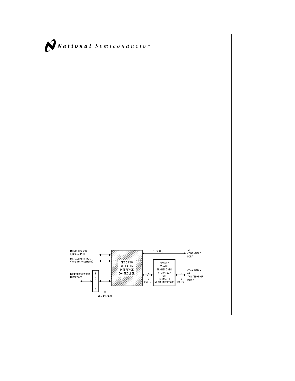
1.0 System Diagram
Simple RIC Hub
TL/F/11096– 1
TRI-STATEÉis a registered trademark of National Semiconductor Corporation.
TM
RIC
and SONICTMare trademarks of National Semiconductor Corporation.
C
1995 National Semiconductor Corporation RRD-B30M16/Printed in U. S. A.
TL/F/11096
Page 2

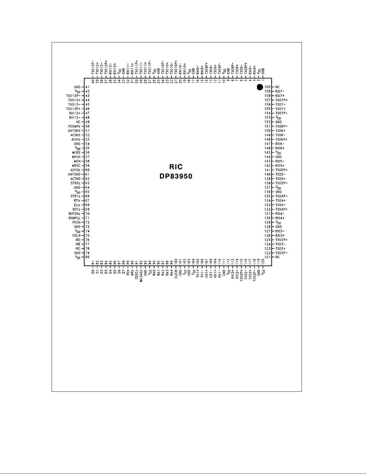
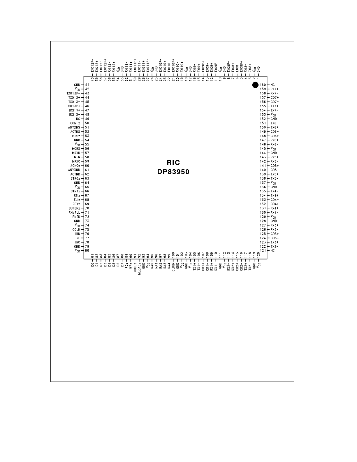
2.0 Connection DiagramÐ160 Pin PQFP Package
Pin Table (12 T.P. Portsa1 AUI Bottom View)
Pin Name Pin No.
b
TXO12P
a
TXO12
b
TXO12
a
TXO12P
b
RXI12
a
RXI12
V
CC
GND 33
b
RXI11
a
RXI11
a
TXO11P
b
TXO11
a
TXO11
b
TXO11P
V
CC
GND 25
b
TXO10P
a
TXO10
b
TXO10
a
TXO10P
b
RXI10
a
RXI10
V
CC
GND 17
b
RXI9
a
RXI9
a
TXO9P
b
TXO9
a
TXO9
b
TXO9P
V
CC
GND 9
b
TXO8P
a
TXO8
b
TXO8
a
TXO8P
b
RXI8
a
RXI8
V
CC
GND 1
Note: NCeNo Connect
40
39
38
37
36
35
34
32
31
30
29
28
27
26
24
23
22
21
20
19
18
16
15
14
13
12
11
10
8
7
6
5
4
3
2
Pin Name Pin No.
NC 160
b
RXI7
RXI7
TXO7P
TXO7
TXO7
TXO7P
V
CC
a
a
b
a
b
159
158
157
156
155
154
153
GND 152
b
TXO6P
TXO6
TXO6
TXO6P
RXI6
RXI6
V
CC
a
b
a
b
a
151
150
149
148
147
146
145
GND 144
b
RXI5
RXI5
TXO5P
TXO5
TXO5
TXO5P
V
CC
a
a
b
a
b
143
142
141
140
139
138
137
GND 136
b
TXO4P
TXO4
TXO4
TXO4P
RXI4
RXI4
V
CC
a
b
a
b
a
135
134
133
132
131
130
129
GND 128
b
RXI3
RXI3
TXO3P
TXO3
TXO3
TXO3P
a
a
b
a
b
127
126
125
124
123
122
NC 121
Pin Name Pin No.
V
CC
GND 119
b
TXO2P
a
TXO2
b
TXO2
a
TXO2P
b
RXI2
a
RXI2
V
CC
GND 111
b
RX1
a
RX1
b
CD1
a
CD1
b
TX1
a
TX1
V
CC
GND 103
V
CC
GND 101
CLKIN 100
RA4 99
RA3 98
RA2 97
RA1 96
RA0 95
V
CC
GND 93
MLOAD 92
CDEC 91
WR 90
RD 89
D7 88
D6 87
D5 86
D4 85
D3 84
D2 83
D1 82
D0 81
120
118
117
116
115
114
113
112
110
109
108
107
106
105
104
102
94
Pin Name Pin No.
V
CC
80
GND 79
IRC 78
IRE 77
IRD 76
COLN 75
V
CC
74
GND 73
PKEN 72
RXMPLL 71
BUFEN 70
RDY 69
ELI 68
RTI 67
STR1 66
V
CC
65
GND 64
STR0 63
ACTND 62
ANYXND 61
ACKO 60
MRXC 59
MEN 58
MRXD 57
MCRS 56
V
CC
55
GND 54
ACKI 53
ACTNS 52
ANYXNS 51
PCOMP 50
NC 49
b
RXI13
RXI13
TXO13P
TXO13
TXO13
TXO13P
V
CC
a
a
b
a
b
48
47
46
45
44
43
42
GND 41
2
Page 3
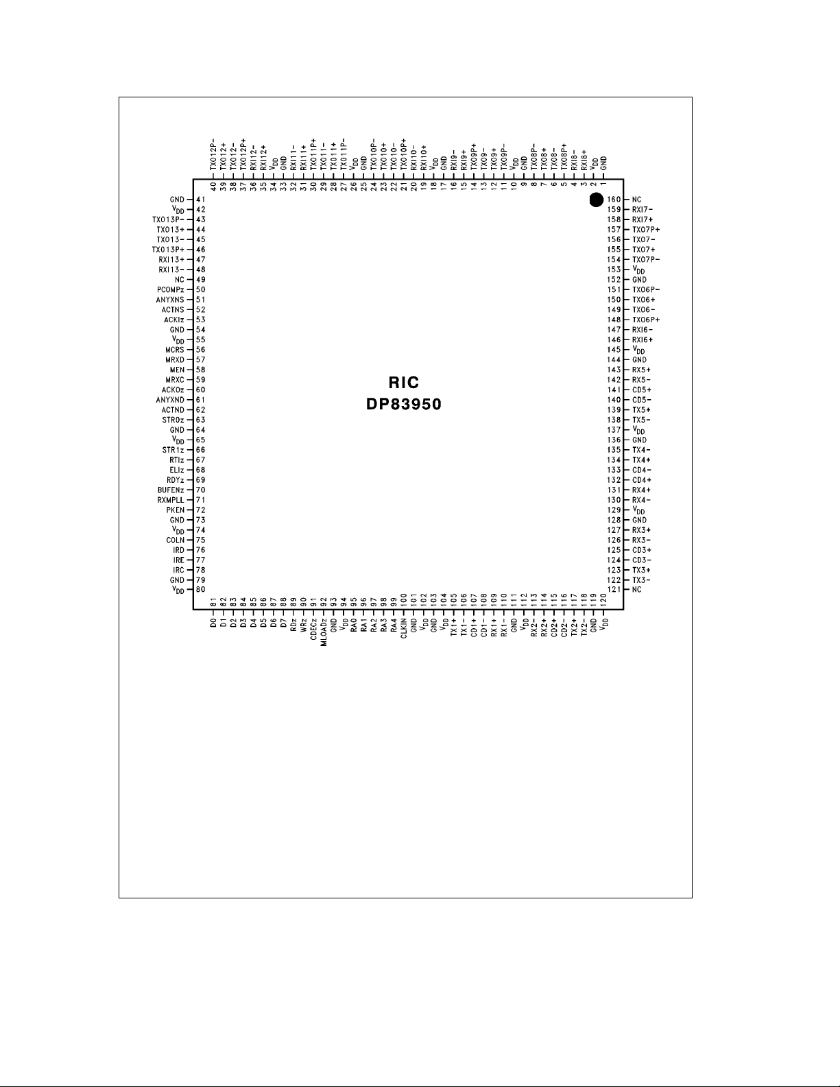
2.0 Connection DiagramÐ160 Pin PQFP Package (Continued)
Ports 2–13 TP
Port 1 AUI
Order Number DP83950BVQB
See NS Package Number VUL160A
3
TL/F/11096– 42
Page 4
2.0 Connection DiagramÐ160 Pin PQFP Package (Continued)
a
6–13 T.P. Ports)
Pin Name Pin No.
V
CC
GND 119
b
TX2
a
TX2
b
CD2
a
CD2
a
RX2
b
RX2
V
CC
GND 111
b
RX1
a
RX1
b
CD1
a
CD1
b
TX1
a
TX1
V
CC
GND 103
V
CC
GND 101
CLKIN 100
RA4 99
RA3 98
RA2 97
RA1 96
RA0 95
V
CC
GND 93
MLOAD 92
CDEC 91
WR 90
RD 89
D7 88
D6 87
D5 86
D4 85
D3 84
D2 83
D1 82
D0 81
120
118
117
116
115
114
113
112
110
109
108
107
106
105
104
102
94
Pin Name Pin No.
b
TXO12P
a
TXO12
b
TXO12
a
TXO12P
b
RXI12
a
RXI12
V
CC
GND 33
b
RXI11
a
RXI11
a
TXO11P
b
TXO11
a
TXO11
b
TXO11P
V
CC
GND 25
b
TXO10P
a
TXO10
b
TXO10
a
TXO10P
b
RXI10
a
RXI10
V
CC
GND 17
b
RXI9
a
RXI9
a
TXO9P
b
TXO9
a
TXO9
b
TXO9P
V
CC
GND 9
b
TXO8P
a
TXO8
b
TXO8
a
TXO8P
b
RXI8
a
RXI8
V
CC
GND 1
Note: NCeNo Connect
Pin Table (1–5 AUI
Pin Name Pin No.
40
39
38
37
36
35
34
32
31
30
29
28
27
26
24
23
22
21
20
19
18
16
15
14
13
12
11
10
8
7
6
5
4
3
2
NC 160
b
RXI7
RXI7
TXO7P
TXO7
TXO7
TXO7P
V
CC
a
a
b
a
b
159
158
157
156
155
154
153
GND 152
b
TXO6P
TXO6
TXO6
TXO6P
RXI6
RXI6
V
CC
a
b
a
b
a
151
150
149
148
147
146
145
GND 144
a
RX5
RX5
CD5
CD5
TX5
TX5
V
CC
b
a
b
a
b
143
142
141
140
139
138
137
GND 136
b
TX4
TX4
CD4
CD4
RX4
RX4
V
CC
a
b
a
a
b
135
134
133
132
131
130
129
GND 128
a
RX3
RX3
CD3
CD3
TX3
TX3
b
a
b
a
b
127
126
125
124
123
122
NC 121
Pin Name Pin No.
V
CC
80
GND 79
IRC 78
IRE 77
IRD 76
COLN 75
V
CC
74
GND 73
PKEN 72
RXMPLL 71
BUFEN 70
RDY 69
ELI 68
RTI 67
STR1 66
V
CC
65
GND 64
STR0 63
ACTND 62
ANYXND 61
ACKO 60
MRXC 59
MEN 58
MRXD 57
MCRS 56
V
CC
55
GND 54
ACKI 53
ACTNS 52
ANYXNS 51
PCOMP 50
NC 49
b
RXI13
RXI13
TXO13P
TXO13
TXO13
TXO13P
V
CC
a
a
b
a
b
48
47
46
45
44
43
42
GND 41
4
Page 5
2.0 Connection DiagramÐ160 Pin PQFP Package (Continued)
Ports 6–13 TP
Ports 1–5 AUI
Order Number DP83950BVQB
See NS Package Number VUL160A
5
TL/F/11096– 43
Page 6

2.0 Connection DiagramÐ160 Pin PQFP Package (Continued)
a
8–13 T.P. Ports)
Pin Name Pin No.
V
CC
GND 119
b
TX2
a
TX2
b
CD2
a
CD2
a
RX2
b
RX2
V
CC
GND 111
b
RX1
a
RX1
b
CD1
a
CD1
b
TX1
a
TX1
V
CC
GND 103
V
CC
GND 101
CLKIN 100
RA4 99
RA3 98
RA2 97
RA1 96
RA0 95
V
CC
GND 93
MLOAD 92
CDEC 91
WR 90
RD 89
D7 88
D6 87
D5 86
D4 85
D3 84
D2 83
D1 82
D0 81
120
118
117
116
115
114
113
112
110
109
108
107
106
105
104
102
94
Pin Name Pin No.
b
TXO12P
a
TXO12
b
TXO12
a
TXO12P
b
RXI12
a
RXI12
V
CC
GND 33
b
RXI11
a
RXI11
a
TXO11P
b
TXO11
a
TXO11
b
TXO11P
V
CC
GND 25
b
TXO10P
a
TXO10
b
TXO10
a
TXO10P
b
RXI10
a
RXI10
V
CC
GND 17
b
RXI9
a
RXI9
a
TXO9P
b
TXO9
a
TXO9
b
TXO9P
V
CC
GND 9
b
TXO8P
a
TXO8
b
TXO8
a
TXO8P
b
RXI8
a
RXI8
V
CC
GND 1
Note: NCeNo Connect
Pin Table (1–7 AUI
Pin Name Pin No.
40
39
38
37
36
35
34
32
31
30
29
28
27
26
24
23
22
21
20
19
18
16
15
14
13
12
11
10
8
7
6
5
4
3
2
NC 160
a
RX7
RX7
CD7
CD7
TX7
TX7
V
CC
b
a
b
a
b
159
158
157
156
155
154
153
GND 152
b
TX6
TX6
CD6
CD6
RX6
RX6
V
CC
a
b
a
a
b
151
150
149
148
147
146
145
GND 144
a
RX5
RX5
CD5
CD5
TX5
TX5
V
CC
b
a
b
a
b
143
142
141
140
139
138
137
GND 136
b
TX4
TX4
CD4
CD4
RX4
RX4
V
CC
a
b
a
a
b
135
134
133
132
131
130
129
GND 128
a
RX3
RX3
CD3
CD3
TX3
TX3
b
a
b
a
b
127
126
125
124
123
122
NC 121
Pin Name Pin No.
V
CC
80
GND 79
IRC 78
IRE 77
IRD 76
COLN 75
V
CC
74
GND 73
PKEN 72
RXMPLL 71
BUFEN 70
RDY 69
ELI 68
RTI 67
STR1 66
V
CC
65
GND 64
STR0 63
ACTND 62
ANYXND 61
ACKO 60
MRXC 59
MEN 58
MRXD 57
MCRS 56
V
CC
55
GND 54
ACKI 53
ACTNS 52
ANYXNS 51
PCOMP 50
NC 49
b
RXI13
RXI13
TXO13P
TXO13
TXO13
TXO13P
V
CC
a
a
b
a
b
48
47
46
45
44
43
42
GND 41
6
Page 7
2.0 Connection DiagramÐ160 Pin PQFP Package (Continued)
Ports 8–13 TP
Ports 1–7 AUI
Order Number DP83950BVQB
See NS Package Number VUL160A
7
TL/F/11096– 44
Page 8
2.0 Connection DiagramÐ160 Pin PQFP Package (Continued)
Pin Table (All AUI Ports)
Pin Name Pin No.
b
TX12
a
TX12
b
CD12
a
CD12
a
RX12
b
RX12
V
CC
GND 33
a
RX11
b
RX11
a
CD11
b
CD11
a
TX11
b
TX11
V
CC
GND 25
b
TX10
a
TX10
b
CD10
a
CD10
a
RX10
b
RX10
V
CC
GND 17
a
RX9
b
RX9
a
CD9
b
CD9
a
TX9
b
TX9
V
CC
GND 9
b
TX8
a
TX8
b
CD8
a
CD8
a
RX8
b
RX8
V
CC
GND 1
Note: NCeNo Connect
40
39
38
37
36
35
34
32
31
30
29
28
27
26
24
23
22
21
20
19
18
16
15
14
13
12
11
10
8
7
6
5
4
3
2
Pin Name Pin No.
NC 160
a
RX7
RX7
CD7
CD7
TX7
TX7
V
CC
b
a
b
a
b
159
158
157
156
155
154
153
GND 152
b
TX6
TX6
CD6
CD6
RX6
RX6
V
CC
a
b
a
a
b
151
150
149
148
147
146
145
GND 144
a
RX5
RX5
CD5
CD5
TX5
TX5
V
CC
b
a
b
a
b
143
142
141
140
139
138
137
GND 136
b
TX4
TX4
CD4
CD4
RX4
RX4
V
CC
a
b
a
a
b
135
134
133
132
131
130
129
GND 128
a
RX3
RX3
CD3
CD3
TX3
TX3
b
a
b
a
b
127
126
125
124
123
122
NC 121
Pin Name Pin No.
V
CC
120
GND 119
b
TX2
TX2
CD2
CD2
RX2
RX2
V
CC
a
b
a
a
b
118
117
116
115
114
113
112
GND 111
b
RX1
RX1
CD1
CD1
TX1
TX1
V
CC
a
b
a
b
a
110
109
108
107
106
105
104
GND 103
V
CC
102
GND 101
CLKIN 100
RA4 99
RA3 98
RA2 97
RA1 96
RA0 95
V
CC
94
GND 93
MLOAD 92
CDEC 91
WR 90
RD 89
D7 88
D6 87
D5 86
D4 85
D3 84
D2 83
D1 82
D0 81
Pin Name Pin No.
V
CC
80
GND 79
IRC 78
IRE 77
IRD 76
COLN 75
V
CC
74
GND 73
PKEN 72
RXMPLL 71
BUFEN 70
RDY 69
ELI 68
RTI 67
STR1 66
V
CC
65
GND 64
STR0 63
ACTND 62
ANYXND 61
ACKO 60
MRXC 59
MEN 58
MRXD 57
MCRS 56
V
CC
55
GND 54
ACKI 53
ACTNS 52
ANYXNS 51
PCOMP 50
NC 49
a
RX13
RX13
CD13
CD13
TX13
TX13
V
CC
b
a
b
a
b
48
47
46
45
44
43
42
GND 41
8
Page 9
2.0 Connection DiagramÐ160 Pin PQFP Package (Continued)
All AUI Ports
Order Number DP83950BVQB
See NS Package Number VUL160A
9
TL/F/11096– 45
Page 10

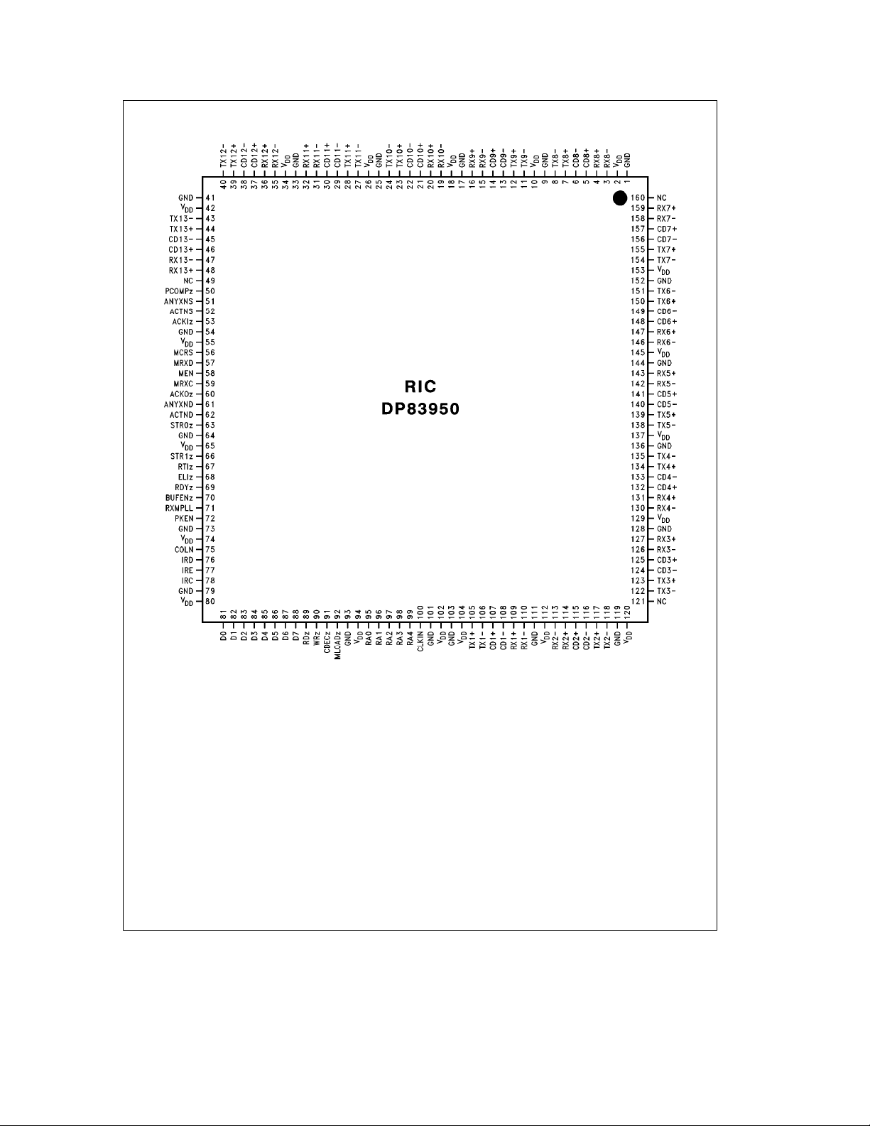
2.0 Connection DiagramÐ160 Pin PGA Package (Continued)
a
1 AUI Bottom View)
Pin Name Pin No.
V
CC
S1
GND P4
b
TXO2P
TXO2
TXO2
TXO2P
RXI2
RXI2
V
CC
a
b
a
b
a
S2
S3
R4
P5
R5
S4
S5
GND S6
b
RX1
RX1
CD1
CD1
TX1
TX1
V
CC
a
b
a
b
a
P6
R6
S7
R7
P7
P8
R8
GND S8
V
CC
S9
GND R9
CLKIN P9
RA4 S10
RA3 R10
RA2 S11
RA1 P10
RA0 R11
V
CC
S12
GND R12
MLOAD P11
CDEC S13
WR R13
RD S14
D7 P12
D6 R14
D5 S15
D4 P13
D3 P14
D2 R15
D1 S16
D0 R16
Pin Name Pin No.
b
TXO12P
a
TXO12
b
TXO12
a
TXO12P
b
RXI12
a
RXI12
V
CC
GND C11
b
RXI11
a
RXI11
a
TXO11P
b
TXO11
a
TXO11
b
TXO11P
V
CC
GND B9
b
TXO10P
a
TXO10
b
TXO10
a
TXO10P
b
RXI10
a
RXI10
V
CC
GND A7
b
RXI9
a
RXI9
a
TXO9P
b
TXO9
a
TXO9
b
TXO9P
V
CC
GND B4
b
TXO8P
a
TXO8
b
TXO8
a
TXO8P
b
RXI8
a
RXI8
V
CC
GND D3
Note: NCeNo Connect
A15
A14
B14
C13
B13
A13
C12
B12
B11
A12
A11
C10
A10
B10
C9
C8
A9
A8
B8
B7
C7
A6
B6
C6
C5
B5
A5
A4
C4
A3
C3
D4
B3
B2
A2
Pin Table (12 T.P. Ports
Pin Name Pin No.
b
RXI7
RXI7
TXO7P
TXO7
TXO7
TXO7P
V
CC
a
a
b
a
b
C2
A1
B1
D2
E3
F3
C1
GND D1
b
TXO6P
TXO6
TXO6
TXO6P
RXI6
RXI6
a
b
a
b
a
E2
G3
F2
E1
G2
H3
NC F1
NC G1
V
CC
H2
GND J3
b
RXI5
RXI5
TXO5P
TXO5
TXO5
TXO5P
V
CC
a
a
b
a
b
J2
H1
J1
K1
K3
K2
L1
GND L2
b
TXO4P
TXO4
TXO4
TXO4P
RXI4
RXI4
V
CC
a
b
a
b
a
M1
L3
M2
N1
N2
M3
P1
GND R1
b
RXI3
RXI3
TXO3P
TXO3
TXO3
TXO3P
a
a
b
a
b
P2
N3
P3
R2
N4
R3
Pin Name Pin No.
V
CC
N13
GND P15
IRC N14
IRE P16
IRD N15
COLN N16
V
CC
M15
GND M14
PKEN L14
RXM L15
BUFEN M16
RDY L16
ELI K16
RTI K14
STR1 K15
V
CC
J16
GND J15
STR0 J14
ACTND H16
ANYXND H15
ACKO H14
MRXC G14
MEN G15
MRXD G16
MCRS F16
V
CC
F14
GND F15
ACKI E15
ACTNS E14
ANYXNS E16
PCOMP D16
b
RXI13
RXI13
TXO13P
TXO13
TXO13
TXO13P
V
CC
a
b
a
D15
D14
a
C16
C15
B16
b
B15
D13
GND C14
10
Page 11
2.0 Connection DiagramÐ160 Pin PGA Package (Continued)
Bottom View
a
1 AUI
2–13 T.P. Ports
Order Number DP83950BNU
See NS Package Number UP159A
11
TL/F/11096– 2
Page 12

2.0 Connection DiagramÐ160 Pin PGA Package (Continued)
a
6–13 T.P. Ports)
Pin Name Pin No.
V
CC
GND P4
b
TX2
a
TX2
b
CD2
a
CD2
a
RX2
b
RX2
V
CC
GND S6
b
RX1
a
RX1
b
CD1
a
CD1
b
TX1
a
TX1
V
CC
GND S8
V
CC
GND R9
CLKIN P9
RA4 S10
RA3 R10
RA2 S11
RA1 P10
RA0 R11
V
CC
GND R12
MLOAD P11
CDEC S13
WR R13
RD S14
D7 P12
D6 R14
D5 S15
D4 P13
D3 P14
D2 R15
D1 R16
D0 R16
S1
S2
S3
R4
P5
R5
S4
S5
P6
R6
S7
R7
P7
P8
R8
S9
S12
Pin Name Pin No.
b
TXO12P
a
TXO12
b
TXO12
a
TXO12P
b
RXI12
a
RXI12
V
CC
GND C11
b
RXI11
a
RXI11
a
TXO11P
b
TXO11
a
TXO11
b
TXO11P
V
CC
GND B9
b
TXO10P
a
TXO10
b
TXO10
a
TXO10P
b
RXI10
a
RXI10
V
CC
GND A7
b
RXI9
a
RXI9
a
TXO9P
b
TXO9
a
TXO9
b
TXO9P
V
CC
GND B4
b
TXO8P
a
TXO8
b
TXO8
a
TXO8P
b
RXI8
a
RXI8
V
CC
GND D3
Note: NCeNo Connect
A15
A14
B14
C13
B13
A13
C12
B12
B11
A12
A11
C10
A10
B10
C9
C8
A9
A8
B8
B7
C7
A6
B6
C6
C5
B5
A5
A4
C4
A3
C3
D4
B3
B2
A2
Pin Table (1–5 AUI
Pin Name Pin No.
b
RXI7
RXI7
TXO7P
TXO7
TXO7
TXO7P
V
CC
a
a
b
a
b
C2
A1
B1
D2
E3
F3
C1
GND D1
b
TXO6P
TXO6
TXO6
TXO6P
RXI6
RXI6
a
b
a
b
a
E2
G3
F2
E1
G2
H3
NC F1
NC G1
V
CC
H2
GND J3
a
RX5
RX5
CD5
CD5
TX5
TX5
V
CC
b
a
b
a
b
J2
H1
J1
K1
K3
K2
L1
GND L2
b
TX4
TX4
CD4
CD4
RX4
RX4
V
CC
a
b
a
a
b
M1
L3
M2
N1
N2
M3
P1
GND R1
a
RX3
RX3
CD3
CD3
TX3
TX3
b
a
b
a
b
P2
N3
P3
R2
N4
R3
Pin Name Pin No.
V
CC
N13
GND P15
IRC N14
IRE P16
IRD N15
COLN N16
V
CC
M15
GND M14
PKEN L14
RXM L15
BUFEN M16
RDY L16
ELI K16
RTI K14
STR1 K15
V
CC
J16
GND J15
STR0 J14
ACTND H16
ANYXND H15
ACKO H14
MRXC G14
MEN G15
MRXD G16
MCRS F16
V
CC
F14
GND F15
ACKI E15
ACTNS E14
ANYXNS E16
PCOMP D16
b
RXI13
RXI13
TXO13P
TXO13
TXO13
TXO13P
V
CC
a
b
a
D15
D14
a
C16
C15
B16
b
B15
D13
GND C14
12
Page 13
2.0 Connection DiagramÐ160 Pin PGA Package (Continued)
Bottom View
a
1–5 AUI
Order Number DP83950BNU
See NS Package Number UP159A
6–13 T.P. Ports
13
TL/F/11096– 3
Page 14
2.0 Connection DiagramÐ160 Pin PGA Package (Continued)
a
8–13 T.P. Ports)
Pin Name Pin No.
V
CC
GND P4
b
TX2
a
TX2
b
CD2
a
CD2
a
RX2
b
RX2
V
CC
GND S6
b
RX1
a
RX1
b
CD1
a
CD1
b
TX1
a
TX1
V
CC
GND S8
V
CC
GND R9
CLKIN P9
RA4 S10
RA3 R10
RA2 S11
RA1 P10
RA0 R11
V
CC
GND R12
MLOAD P11
CDEC S13
WR R13
RD S14
D7 P12
D6 R14
D5 S15
D4 P13
D3 P14
D2 R15
D1 S16
D0 R16
S1
S2
S3
R4
P5
R5
S4
S5
P6
R6
S7
R7
P7
P8
R8
S9
S12
Pin Name Pin No.
b
TXO12P
a
TXO12
b
TXO12
a
TXO12P
b
RXI12
a
RXI12
V
CC
GND C11
b
RXI11
a
RXI11
a
TXO11P
b
TXO11
a
TXO11
b
TXO11P
V
CC
GND B9
b
TXO10P
a
TXO10
b
TXO10
a
TXO10P
b
RXI10
a
RXI10
V
CC
GND A7
b
RXI9
a
RXI9
a
TXO9P
b
TXO9
a
TXO9
b
TXO9P
V
CC
GND B4
b
TXO8P
a
TXO8
b
TXO8
a
TXO8P
b
RXI8
a
RXI8
V
CC
GND D3
Note: NCeNo Connect
A15
A14
B14
C13
B13
A13
C12
B12
B11
A12
A11
C10
A10
B10
C9
C8
A9
A8
B8
B7
C7
A6
B6
C6
C5
B5
A5
A4
C4
A3
C3
D4
B3
B2
A2
Pin Table (1–7 AUI
Pin Name Pin No.
a
RX7
RX7
CD7
CD7
TX7
TX7
V
CC
b
a
b
a
b
C2
A1
B1
D2
E3
F3
C1
GND D1
b
TX6
TX6
CD6
CD6
RX6
RX6
a
b
a
a
b
E2
G3
F2
E1
G2
H3
NC F1
NC G1
V
CC
H2
GND J3
a
RX5
RX5
CD5
CD5
TX5
TX5
V
CC
b
a
b
a
b
J2
H1
J1
K1
K3
K2
L1
GND L2
b
TX4
TX4
CD4
CD4
RX4
RX4
V
CC
a
b
a
a
b
M1
L3
M2
N1
N2
M3
P1
GND R1
a
RX3
RX3
CD3
CD3
TX3
TX3
b
a
b
a
b
P2
N3
P3
R2
N4
R3
Pin Name Pin No.
V
CC
N13
GND P15
IRC N14
IRE P16
IRD N15
COLN N16
V
CC
M15
GND M14
PKEN L14
RXM L15
BUFEN M16
RDY L16
ELI K16
RTI K14
STR1 K15
V
CC
J16
GND J15
STR0 J14
ACTND H16
ANYXND H15
ACKO H14
MRXC G14
MEN G15
MRXD G16
MCRS F16
V
CC
F14
GND F15
ACKI E15
ACTNS E14
ANYXNS E16
PCOMP D16
b
RXI13
RXI13
TXO13P
TXO13
TXO13
TXO13P
V
CC
a
b
a
D15
D14
a
C16
C15
B16
b
B15
D13
GND C14
14
Page 15

2.0 Connection DiagramÐ160 Pin PGA Package (Continued)
Bottom View
a
1–7 AUI
Order Number DP83950BNU
See NS Package Number UP159A
8–13 T.P. Ports
15
TL/F/11096– 4
Page 16

2.0 Connection DiagramÐ160 Pin PGA Package (Continued)
Pin Table ( All AUI Ports)
Pin Name Pin No.
b
TX12
a
TX12
b
CD12
a
CD12
a
RX12
b
RX12
V
CC
GND C11
a
RX11
b
RX11
a
CD11
b
CD11
a
TX11
b
TX11
V
CC
GND B9
b
TX10
a
TX10
b
CD10
a
CD10
a
RX10
b
RX10
V
CC
GND A7
a
RX9
b
RX9
a
CD9
b
CD9
a
TX9
b
TX9
V
CC
GND B4
b
TX8
a
TX8
b
CD8
a
CD8
a
RX8
b
RX8
V
CC
GND D3
Note: NCeNo Connect
A15
A14
B14
C13
B13
A13
C12
B12
B11
A12
A11
C10
A10
B10
C9
C8
A9
A8
B8
B7
C7
A6
B6
C6
C5
B5
A5
A4
C4
A3
C3
D4
B3
B2
A2
Pin Name Pin No.
a
RX7
RX7
CD7
CD7
TX7
TX7
V
CC
b
a
b
a
b
C2
A1
B1
D2
E3
F3
C1
GND D1
b
TX6
TX6
CD6
CD6
RX6
RX6
a
b
a
a
b
E2
G3
F2
E1
G2
H3
NC F1
NC G1
V
CC
H2
GND J3
a
RX5
RX5
CD5
CD5
TX5
TX5
V
CC
b
a
b
a
b
J2
H1
J1
K1
K3
K2
L1
GND L2
b
TX4
TX4
CD4
CD4
RX4
RX4
V
CC
a
b
a
a
b
M1
L3
M2
N1
N2
M3
P1
GND R1
a
RX3
RX3
CD3
CD3
TX3
TX3
b
a
b
a
b
P2
N3
P3
R2
N4
R3
Pin Name Pin No.
V
CC
S1
GND P4
b
TX2
TX2
CD2
CD2
RX2
RX2
V
CC
a
b
a
a
b
S2
S3
R4
P5
R5
S4
S5
GND S6
b
RX1
RX1
CD1
CD1
TX1
TX1
V
CC
a
b
a
b
a
P6
R6
S7
R7
P7
P8
R8
GND S8
V
CC
S9
GND R9
CLKIN P9
RA4 S10
RA3 R10
RA2 S11
RA1 P10
RA0 R11
V
CC
S12
GND R12
MLOAD P11
CDEC S13
WR R13
RD S14
D7 P12
D6 R14
D5 S15
D4 P13
D3 P14
D2 R15
D1 S16
D0 R16
Pin Name Pin No.
V
CC
N13
GND P15
IRC N14
IRE P16
IRD N15
COLN N16
V
CC
M15
GND M14
PKEN L14
RXM L15
BUFEN M16
RDY L16
ELI K16
RTI K14
STR1 K15
V
CC
J16
GND J15
STR0 J14
ACTND H16
ANYXND H15
ACKO H14
MRXC G14
MEN G15
MRXD G16
MCRS F16
V
CC
F14
GND F15
ACKI E15
ACTNS E14
ANYXNS E16
PCOMP D16
a
RX13
RX13
CD13
CD13
TX13
TX13
V
CC
b
a
b
a
b
D15
D14
C16
C15
B16
B15
D13
GND C14
16
Page 17
2.0 Connection DiagramÐ160 Pin PGA Package (Continued)
Bottom View
All AUI Ports
Order Number DP83950BNU
See NS Package Number UP159A
17
TL/F/11096– 5
Page 18

3.0 Pin Descriptions
Pin Pin Driver
No. Name Type
NETWORK INTERFACE PINS (On-Chip Transceiver Mode)
RXI2bto RXI13
RXI2ato RXI13
TXOP2bto TXOP13
TXO2bto TXO13
TXO2ato TXO13
TXOP2ato TXOP13
a
CD1
b
CD1
a
RX1
b
RX1
a
TX1
b
TX1
b
a
b
b
a
a
TP I Twisted Pair Receive Input Negative
TP I Twisted Pair Receive Input Positive
TT O Twisted Pair Pre-emphasis Transmit Output Negative
TT O Twisted Pair Transmit Output Negative
TT O Twisted Pair Transmit Output Positive
TT O Twisted Pair Pre-emphasis Transmit Output Positive
AL I AUI Collision Detect Input Positive
AL I AUI Collision Detect Input Negative
AL I AUI Receive Input Positive
AL I AUI Receive Input Negative
AD O AUI Transmit Output Positive
AD O AUI Transmit Output Negative
NETWORK INTERFACE PINS (External Transceiver Mode AUI Signal Level Compatibility Selected)
TX2ato TX13
TX2bto TX13
CD2ato CD13
CD2bto CD13
RX2ato RX13
RX2bto RX13
a
CD1
b
CD1
a
RX1
b
RX1
a
TX1
b
TX1
Note: ADeAUI level and Drive compatible, TPeTwisted Pair interface compatible, ALeAUI Level compatible, TTeTTL compatible, IeInput, OeOutput.
a
b
a
b
a
b
AL O Transmit Output Positive
AL O Transmit Output Negative
AL I Collision Input Positive
AL I Collision Input Negative
AL I Receive Input Positive
AL I Receive Input Negative
AL I AUI Collision Detect Input Positive
AL I AUI Collision Detect Input Negative
AL I AUI Receive Input Positive
AL I AUI Receive Input Negative
AD O AUI Transmit Output Positive
AD O AUI Transmit Output Negative
I/O Description
18
Page 19
3.0 Pin Descriptions (Continued)
Pin Pin Driver
No. Name Type
PROCESSOR BUS PINS
RA0–RA4 TT I REGISTER ADDRESS INPUTS: These five pins are used to select a register to be read or
STR0 C O DISPLAY UPDATE STROBE 0
STR1 C O DISPLAY UPDATE STROBE 1
D0–D7 TT B, Z DATA BUS
BUFEN COBUFFER ENABLE: This output controls the TRI-STATEÉoperation of the bus transceiver
RDY C O DATA READY STROBE: The falling edge of this signal during a read cycle indicates that data
ELI COEVENT LOGGING INTERRUPT: A low level on the ELI output indicates the RIC’s hub
RTI COREAL TIME INTERRUPT: A low level on the RTI output indicates the RIC’s real time (packet
CDEC TT I COUNTER DECREMENT: A low level on the CDEC input strobe decrements all of the RIC’s
WR TT I WRITE STROBE: Strobe from the CPU used to write an internal register defined by the
RD TT I READ STROBE: Strobe from the CPU used to read an internal register defined by the RA0 –
MLOAD TT I DEVICE RESET AND MODE LOAD: When this input is low all of the RIC’s state machines,
I/O Description
written. The state of these inputs are ignored when the read, write and mode load input strobes
are high. (Even under these conditions these inputs must not be allowed to float at an
undefined logic state).
Maximum Display Mode: This signal controls the latching of display data for network ports 1
to 7 into the off chip display latches.
Minimum Display Mode: This signal controls the latching of display data for the RIC into the
off chip display latch.
During processor access cycles (read or write is asserted) this signal is inactive (high).
Maximum Display Mode: This signal controls the latching of display data for network ports 8
to 13 into the off chip display latches.
Minimum Display Mode: No operation
During processor access cycles (read or write is asserted) this signal is inactive (high).
Display Update Cycles: These pins become outputs providing display data and port address
information. Address information only available in Maximum Display mode.
Processor Access Cycles: Data input or output is performed via these pins. The read, write
and mode load inputs control the direction of the signals.
Note: The data pins remain in their display update function, i.e., asserted as outputs unless either the read or
write strobe is asserted.
which provides the interface between the RIC’s data pins and the processor’s data bus.
Note: The buffer enable output indicates the function of the data pins. When it is high they are performing
display update cycles, when it is low a processor access or mode load cycle is occurring.
is stable and valid for sampling. In write cycles the falling edge of RDY
data has been latched by the RIC. Therefore data must have been available and stable for this
operation to be successful.
management logic requires CPU attention. The interrupt is cleared by accessing the Port Event
Recording register or Event Counter that produced it. All interrupt sources may be masked.
specific) interrupt logic requires CPU attention. The interrupt is cleared by reading the Real
Time Interrupt Status register. All interrupt sources may be masked.
Port Event Counters by one. This input is internally synchronized and if necessary the
operation of the signal is delayed if there is a simultaneous internally generated counting
operation.
RA0–RA4 inputs.
RA4 inputs.
counters and network ports are reset and held inactive. On the rising edge of MLOAD
levels present on the D0–7 pins and RA0 –RA4 inputs are latched into the RIC’s configuration
registers. The rising edge of MLOAD
also signals the beginning of the display test operation.
denotes that the write
the logic
19
Page 20

3.0 Pin Descriptions (Continued)
Pin Pin Driver
No. Name Type
INTER-RIC BUS PINS
ACKI TT I ACKNOWLEDGE INPUT: Input to the network ports’ arbitration chain.
ACKO TT O ACKNOWLEDGE OUTPUT: Output from the network ports’ arbitration chain.
IRD TT B, Z INTER-RIC DATA: When asserted as an output this signal provides a serial data stream in NRZ
IRE TT B, Z INTER-RIC ENABLE: When asserted as an output this signal provides an activity framing enable
IRC TT B, Z INTER-RIC CLOCK: When asserted as an output this signal provides a clock signal for the serial
COLN TT B, Z COLLISION ON PORT N: This denotes that a collision is occurring on the port receiving the
PKEN C O PACKET ENABLE: This output acts as an active high enable for an external bus transceiver (if
CLKIN TT I 40 MHz CLOCKINPUT: This input is used to generate the RIC’s timing reference for the state
ACTND OD O ACTIVITY ON PORT NDRIVE: This output is active when the RIC is receiving data or collision
ACTNS TT I ACTIVITY ON PORT NSENSE: This input senses when this or another RIC in a multi-RIC
ANYXND OD O ACTIVITY ON ANY PORT EXCLUDING PORT NDRIVE: This output is active when a RIC is
ANYXNS TT I ACTIVITY ON ANY PORT EXCLUDING PORT NSENSE: This input senses when this RIC or
I/O Description
format. The signal is asserted by a RIC when it is receiving data from one of its network
segments. The default condition of this signal is to be an input. In this state it may be driven by
other devices on the Inter-RIC bus.
for the serial data stream. The signal is asserted by a RIC when it is receiving data from one of
its network segments. The default condition of this signal is to be an input. In this state it may be
driven by other devices on the Inter-RIC bus.
data stream. Data (IRD) is changed on the falling edge of the clock. The signal is asserted by a
RIC when it is receiving data from one of its network segments. The default condition of this
signal is to be an input. When an input IRD is sampled on the rising edge of the clock. In this
state it may be driven by other devices on the Inter-RIC bus.
data packet. The default condition of this signal is to be an input. In this state it may be driven by
other devices on the Inter-RIC bus.
required) for the IRE, IRC IRD and COLN signals. When high the bus transceiver should be
transmitting on to the bus, i.e., this RIC is driving the IRD, IRE, IRC and COLN bus lines. When
low the bus transceiver should receive from the bus.
machines, and phase lock loop decoder.
information from one of its network segments.
system is receiving data or collision information.
experiencing a transmit collision or multiple ports have active collisions on their network
segments.
other RICs in a multi-RIC system are experiencing transmit collisions or multiple ports have
active collisions on their network segments.
20
Page 21
3.0 Pin Descriptions (Continued)
Pin Pin Driver
No. Name Type
MANAGEMENT BUS PINS
MRXC TT O, Z MANAGEMENT RECEIVE CLOCK: When asserted this signal provides a clock signal for the
MCRS TT B, Z MANAGEMENT CARRIERSENSE: When asserted this signal provides an activity framing
MRXD TT O, Z MANAGEMENT RECEIVE DATA: When asserted this signal provides a serial data stream in NRZ
MEN C O MANAGEMENT BUS OUTPUT ENABLE: This output acts as an active high enable for an
PCOMP TT I PACKET COMPRESS: This input is used to activate the RIC’s packet compress logic. A low level
POWER AND GROUND PINS
V
CC
GND Negative Supply
EXTERNAL DECODER PINS
RXM TT O RECEIVE DATA MANCHESTER FORMAT: This output makes the data, in Manchester format,
Note: TTeTTL compatible, BeBi-directional, CeCMOS compatible, ODeOpen Drain, IeInput, OeOutput, ZeTRI-STATE
I/O Description
MRXD serial data stream. The MRXD signal is changed on the falling edge of this clock. The
signal is asserted when a RIC is receiving data from one of its network segements. Otherwise the
signal is inactive.
enable for the serial output data stream (MRXD). The signal is asserted when a RIC is receiving
data from one of its network segments. Otherwise the signal is an input.
format. The data stream is made up of the data packet and RIC status information. The signal is
asserted when a RIC is receiving data from one of its network segments. Otherwise the signal is
inactive.
external bus transceiver (if required) for the MRXC, MCRS and MRXD signals. When high the bus
transceiver should be transmitting on to the bus.
on this signal when MCRS is active will cause that packet to be compressed. If PCOMP
low all packets are compressed, if PCOMP
Positive Supply
received by port N available for test purposes. If not used for testing this pin should be left open.
is tied high packet compression is inhibited.
is tied
21
Page 22
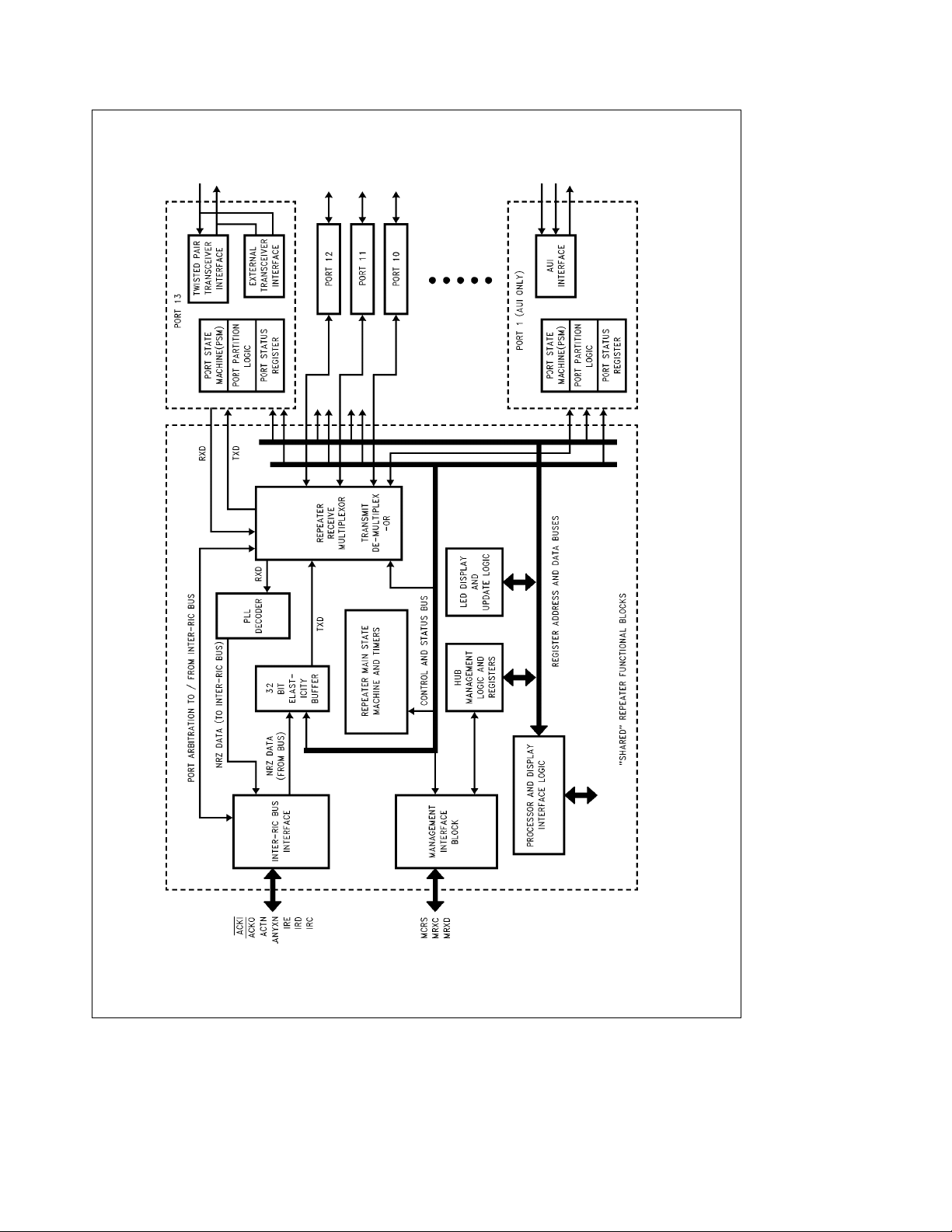
4.0 Block Diagram
TL/F/11096– 6
FIGURE 5.1
22
Page 23

5.0 Functional Description
The I.E.E.E. repeater specification details a number of functions a repeater system must perform. These requirements
allied with a need for the implementation to be multiport
strongly favors the choice of a modular design style. In such
a design, functionality is split between those tasks common
to all data channels and those exclusive to each individual
channel. The RIC follows this approach, certain functional
blocks are replicated for each network attachment, (also
known as a repeater port), and others are shared. The following section briefly describes the functional blocks in the
RIC.
5.1 OVERVIEW OF RIC FUNCTIONS
Segment Specific Block: Network Port
As shown in the Block Diagram, the segment specific blocks
consist of:
1. One or more physical layer interfaces.
2. A logic block required for performing repeater operations
upon that particular segment. This is known as the ‘‘port’’
logic since it is the access ‘‘port’’ the segment has to the
rest of the network.
This function is repeated 13 times in the RIC (one for each
port) and is shown on the right side of the Block Diagram,
Figure 5.1
The physical layer interfaces provided depends upon the
port under examination. Port 1 has an AUI compliant interface for use with AUI compatible transceiver boxes and cable. Ports 2 to 13 may be configured for use with one of two
interfaces: twisted pair or an external transceiver. The former utilizes the RIC’s on-chip 10BASE-T transceivers, the
latter allows connection to external transceivers. When using the external transceiver mode the interface is AUI compatible. Although AUI compatible transceivers are supported the interface is not designed for use with an interface
cable, thus the transceivers are necessarily internal to the
repeater equipment.
Inside the port logic there are 3 distinct functions:
1. The port state machine ‘‘PSM’’ is required to perform
2. The port partition logic implements the segment partition-
3. The port status register reflects the current status of the
Shared Functional Blocks:
Repeater Core Logic
The shared functional blocks consist of the Repeater Main
State Machine (MSM) and Timers, a 32 bit Elasticity Buffer,
PLL Decoder, and Receive and Transmit Multiplexors.
These blocks perform the majority of the operations needed
to fulfill the requirements of the IEEE repeater specification.
When a packet is received by a port it is sent via the Receive Multiplexor to the PLL Decoder. Notification of the
.
data and collision repetition as described by the repeater
specification, for example, it determines whether this port
should be receiving from or transmitting to its network
segment.
ing algorithm. This algorithm is defined by the IEEE specification and is used to protect the network from malfunctioning segements.
port. It may be accessed by a system processor to obtain
this status or to perform certain port configuration operations, such as port disable.
data and collision status is sent to the main state machine
via the receive multiplexor and collision activity status signals. This enables the main state machine to determine the
source of the data to be repeated and the type of data to be
transmitted. The transmit data may be either the received
packet’s data field or a preamble/jam pattern consisting of
a 1010 . . . bit pattern.
Associated with the main state machine are a series of timers. These ensure various IEEE specification times (referred
to as the TW1 to TW6 times) are fulfilled.
A repeater unit is required to meet the same signal jitter
performance as any receiving node attached to a network
segment. Consequently, a phase locked loop Manchester
decoder is required so that the packet may be decoded, and
the jitter accumulated over the receiving segment recovered. The decode logic outputs data in NRZ format with an
associated clock and enable. In this form the packet is in a
convenient format for transfer to other devices, such as network controllers and other RICs, via the Inter-RIC bus (described later). The data may then be re-encoded into Manchester data and transmitted.
Reception and transmission via physical layer transceiver
units causes a loss of bits in the preamble field of a data
packet. The repeater specification requires this loss to be
compensated for. To accomplish this an elasticity buffer is
employed to temporarily store bits in the data field of the
packet.
The sequence of operation is as follows:
Soon after the network segment receiving the data packet
has been identified, the RIC begins to transmit the packet
preamble pattern (1010 . . . ) onto the other network segments. While the preamble is being transmitted the Elasticity Buffer monitors the decoded received clock and data signals (this is done via the Inter-RIC bus as described later).
When the start of frame delimiter ‘‘SFD’’ is detected the
received data stream is written into the elasticity buffer. Removal of data from the buffer for retransmission is not allowed until a valid length preamble pattern has been transmitted.
Inter-RIC Bus Interface
Using the RIC in a repeater system allows the design to be
constructed with many more network attachments than can
be supported by a single chip. The split of functions already
described allows data packets and collision status to be
transferred between multiple RICs, and at the same time the
multiple RICs still behave as a single logical repeater. Since
all RICs in a repeater system are identical and capable of
performing any of the repetition operations, the failure of
one RIC will not cause the failure of the entire system. This
is an important issue in large multiport repeaters.
RICs communicate via a specialized interface known as the
Inter-RIC bus. This allows the data packet to be transferred
from the receiving RIC to the other RICs in the system.
These RICs then transmit the data stream to their segments. Just as important as data transfer is the notification
of collisions occurring across the network. The Inter-RIC
bus has a set of status lines capable of conveying collision
information between RICs to ensure their main state machines operate in the appropriate manner.
23
Page 24
5.0 Functional Description (Continued)
LED Interface and Hub Management Function
Repeater systems usually possess optical displays indicating network activity and the status of specific repeater operations. The RIC’s display update block provides the system
designer with a wide variety of indicators. The display updates are completely autonomous and merely require SSI
logic devices to drive the display devices, usually made up
of light emitting diodes, LEDs. The status display is very
flexible allowing the user to choose those indicators appropriate for the specification of the equipment.
The RIC has been designed with special awareness for system designers implementing large repeaters possessing
hub management capabilities. Hub management uses the
unique position of repeaters in a network to gather statistics
about the network segments they are attached to. The RIC
provides hub management statistical data in 3 steps. Important events are gathered by the management block from
logic blocks throughout the chip. These events may then be
stored in on-chip latches or counted in on-chip counters according to user supplied latching and counting masks.
The fundamental task of a hub management system implementation is to associate the current packet and any management status information with the network segment, i.e.,
repeater port where the packet was received. The ideal system would place this combined data packet and status field
in system memory for examination by hub management
software. The ultimate function of the RIC’s hub management support logic is to provide this function.
To accomplish this the RIC utilizes a dedicated hub management interface. This is similar to the Inter-RIC bus since
it allows the data packet to be recovered from the receiving
RIC. Unlike the Inter-RIC bus the intended recipient is not
another RIC but National Semiconductor’s DP83932
TM
‘‘SONIC
allows a management status field to be appended at the
end of the data packet. This can be done without affecting
the operation of the repeater system.
Processor Interface
The RIC’s processor interface allows connection to a system processor. Data transfer occurs via an octal bi-directional data bus. The RIC has a number of on-chip registers
indicating the status of the hub management functions, chip
configuration and port status. These may be accessed by
providing the chosen address at the Register Address
(RA4–RA0) input pins.
Display update cycles and processor accesses occur utilizing the same data bus. An on-chip arbiter in the processor/
display block schedules and controls the accesses and ensures the correct information is written into the display latches. During the display update cycles the RIC behaves as a
master of its data bus. This is the default state of the data
bus. Consequently, a TRI-STATE buffer must be placed between the RIC and the system processor’s data bus. This
’’ Network controller. The use of a dedicated bus
ensures bus contention is avoided during simultaneous display update cycles and processor accesses of other devices on the system bus. When the processor accesses a RIC
register, the RIC enables the data buffer and selects the
operation, either input or output, of the data pins.
5.2 DESCRIPTION OF REPEATER OPERATIONS
In order to implement a multi-chip repeater system which
behaves as though it were a single logical repeater, special
consideration must be paid to the data path used in packet
repetition. For example, where in the path are specific operations such as Manchester decoding and elasticity buffering
performed. Also the system’s state machines which utilize
available network activity signals, must be able to accommodate the various packet repetition and collision scenarios
detailed in the repeater specification.
The RIC contains two types of inter-acting state machines.
These are:
1. Port State Machines (PSMs). Every network attachment
has its own PSM.
2. Main State Machine (MSM). This state machine controls
the shared functional blocks as shown in the block diagram
Figure 5.1.
Repeater Port and Main State Machines
These two state machines are described in the following
sections. Reference is made to expressions used in the
IEEE Repeater specification. For the precise definition of
these terms please refer to the specification. To avoid confusion with the RIC’s implementation, where references are
made to repeater states or terms as described in the IEEE
specification, these items are written in
state diagram is shown in
diagram is shown in
FIGURE 5.2. Inter-RIC Bus State Diagram
Figure 5-3
Figure 5-2
.
italics.
, the Inter-RIC bus state
The IEEE
TL/F/11096– 7
24
Page 25

5.0 Functional Description (Continued)
FIGURE 5.3. IEEE Repeater Main State Diagram
25
TL/F/11096– 8
Page 26

5.0 Functional Description (Continued)
Port State Machine (PSM)
There are two primary functions for the PSM as follows:
1. Control the transmission of repeated data and jam signals over the attached segment.
2. Decide whether a port will be the source of data or collision information which will be repeated over the network.
This repeater port is known as
process is required to enable the repeater to transition
from the
IDLE
or
RECEIVE COLLISION
cess is used to locate the port which will be
that particular packet. The data received from this port is
directed to the PLL decoder and transmitted over the Inter-RIC bus. If the repeater enters the
SION
determine which port is
ed from the repeater’s other ports if the repeater enters
the
ONE PORT LEFT
not transmit to its segment; where as all other ports are
still required to transmit to their segments.
Main State Machine (MSM)
The MSM controls the operation of the shared functional
blocks in each RIC as shown in the block diagram,
5.1
, and it performs the majority of the data and collision
propagation operations as defined by the IEEE specification, these include:
Function Action
Preamble Restore the length of the preamble
Regeneration pattern to the defined size.
Fragment Extend received data or collision
Extension fragments to meet the minimum
Elasticity A portion of the received packet may
Buffer require storage in an Elasticity Buffer to
Control accommodate preamble regeneration.
Jam/ In cases of receive or transmit collisions
Preamble a RIC is required to transmit a jam
Pattern pattern (1010...).
Generation
Transmit Once the
Collision is entered a repeater is required to stay
Enforcement in this state for at least 96 network bit
Data NRZ format data from the elasticity
Encoding buffer must be encoded into Manchester
Control format data prior to retransmission.
Tw1
Enforcement specification.
Tw2
Enforcement specification on all ports with active
state to the
state a further arbitration operation is performed to
state. In this state
fragment length of 96 bits.
Note: This pattern is the same as that used for
preamble regeneration.
times.
Enforce the Transmit Recovery Time
Enforce Carrier Recovery Time
collisions.
PORT N
. An arbitration
SEND PREAMBLE PATTERN
states, see
Figure 5.3
. This pro-
PORT N
TRANSMIT COLLI-
PORT M.PORT M
is differentiat-
PORT M
TRANSMIT COLLISION
does
Figure
state
for
The interaction of the main and port state machines is visible, in part, by observing the Inter-RIC bus.
Inter-RIC Bus Operation
Overview
The Inter-RIC Bus consists of eight signals. These signals
implement a protocol which may be used to connect multiple RICs together. In this configuration, the logical function
of a single repeater is maintained. The resulting multi-RIC
system is compliant to the IEEE 802.3 repeater specification
and may connect several hundred network segments. An
example of a multi-RIC system is shown in
The Inter-RIC Bus connects multiple RICs to realize the following operations:
Port N
Identification (which port the repeater receives
data from)
Port M
Identification (which port is the last one experiencing a collision)
Data Transfer
RECEIVE COLLISION
TRANSMIT COLLISION
DISABLE OUTPUT
The following tables briefly describes the operation of each
bus signal, the conditions required for a RIC to assert a
signal and which RICs (in a multi-RIC system) would monitor
a signal:
Function Input signal to the PSM arbitration
Conditions Not applicable
required for a
RIC to drive
this signal
RIC Receiving This is dependent upon the method
the signal used to cascade RICs, described in
Function Output signal from the PSM
Conditions This is dependent upon the method
required for a used to cascade RICs, described in
RIC to drive a following section.
this signal
RIC Receiving Not applicable
the Signal
identification
identification
(jabber protection)
ACKI
chain. This chain is employed to
identify
PORT N
Note: A RIC which contains
PORT M
may be identified by its ACKO
signal being low when its ACKI input is
high.
a following section.
ACKO
arbitration chain.
and
Figure 5.4
PORT M
PORT N
.
.
or
26
Page 27

5.0 Functional Description (Continued)
ACTN
Function This signal denotes there is activity
Conditions A RIC must contain
required for a
RIC to drive
this signal
RIC Receiving The signal is monitored by all RICs in
the Signal the repeater system.
on
PORT NorPORT M
PORT M
.
Note: Although this signal normally has
only one source asserting the signal active
it is used in a wired-or configuration.
.
PORT N
or
IRD
Function Decoded serial data, in NRZ format,
Conditions A RIC must contain
required for a
RIC to drive
this signal
RIC Receiving The signal is monitored by all other
the Signal RICs in the repeater system.
received from the network segment
attached to
PORT N
.
PORT N
.
ANYXN
Function This signal denotes that a repeater
Conditions Any RIC which satisfies the above
required for a condition.
RIC to drive Note: This bus line is used in a wired-or
this signal
RIC Receiving The signal is monitored by all RICs in
the Signal the repeater system.
Function Denotes
Conditions A RIC must contain
required for a
RIC to drive
this signal
RIC Receiving The Signal is monitored by all other
the Signal RICs in the repeater system.
Function This signal acts as an activity
Conditions A RIC must contain
required for a
RIC to drive
this signal
RIC Receiving The Signal is monitored by all other
the Signal RICs in the repeater system.
Note 1: Refer to note on page 25 for the transmit collision case.
port that is not
is experiencing a collision.
configuration.
PORT NorPORT M
COLN
PORT NorPORT M
experiencing a collision.
PORT N
PORT N
or
.
PORT M
. (Note 1)
IRE
framing signal for the IRC and IRD
signals.
IRC
Function Clock signal associated with IRD
Conditions A RIC must contain
required for a
RIC to drive
this signal
RIC Receiving The signal is monitored by all other
the Signal RICs in the repeater system.
Methods of RIC Cascading
In order to build multi-RIC repeaters
is
identification must be performed across all the RICs in the
system. Inside each RIC the PSMs are arranged in a logical
arbitration chain where port 1 is the highest and port 13 the
lowest. The top of the chain, the input to port 1 is accessible
to the user via the RIC’s ACKI
bottom of the chain becomes the ACKO
single RIC system
the arbitration chain with receive or collision activity.
identification is performed when the repeater is in the
state.
PORT M
with a collision when the repeater leaves the
COLLISION
tion, all that needs to be done is to tie the ACKI
logic high state. In multi-RIC systems there are two methods
to propagate the arbitration chain between RICs:
The first and most straight forward is to extend the arbitration chain by daisy chaining the ACKI
tween RICs. In this approach one RIC is placed at the top of
the chain (its ACKI
from this RIC is sent to the ACKI
so on. This arrangement is simple to implement but it places
some topological restrictions upon the repeater system. In
particular, if the repeater is constructed using a backplane
with removable printed circuit boards. (These boards contain the RICs and their associated components). If one of
the boards is removed then the ACKI
broken and the repeater will not operate correctly.
and IRE.
PORT N
.
PORT N
and
PORT M
input pin. The output from the
PORT N
is defined as the highest port in
output pin. In a
Port N
IDLE
is defined as the highest port in the chain
TRANSMIT
state. In order for the arbitration chain to func-
input is tied high), then the ACKO signal
input of the next RIC and
signal to a
ACKO signals be-
ACKO chain will be
27
Page 28

5.0 Functional Description (Continued)
The second method of
this problem. This second technique relies on an external
parallel arbiter which monitors all of the RIC’s ACKO
and responds to the RIC with the highest priority. In this
scheme each RIC is assigned with a priority level. One
method of doing this is to assign a priority number which
reflects the position of a RIC board on the repeater backplane, i.e., its slot number. When a RIC experiences receive
activity and the repeater system is in the
board will assert ACKO
identification number onto an arbitration bus and the RIC
containing
is used in the
PORT M
the problems caused by missing boards, i.e., empty slots in
the backplane. The logic associated with asserting this arbitration vector in the various packet repetition scenarios
could be implemented in programmable logic type devices.
To perform
methods employ the same signals: ACKI
The Inter-RIC bus allows multi-RIC operations to be performed in exactly the same manner as if there is only a
single RIC in the system. The simplest way to describe the
operation of Inter-RIC bus is to see how it is used in a number of common packet repetition scenarios. Throughout this
description the RICs are presumed to be operating in external transceiver mode. This is advantageous for the explanation since the receive, transmit and collision signals from
each network segment are observable. In internal transceiver mode this is not the case, since the collision signal for the
non-AUI ports is derived by the transceivers inside the RIC.
5.3 EXAMPLES OF PACKET REPETITION SCENARIOS
Data Repetition
The simplest packet operation performed over the Inter-RIC
Bus is data repetition. In this operation a data packet is
received at one port and transmitted to all other segments.
The first task to be performed is
is an arbitration process performed by the Port State Machines in the system. In situations where two or more ports
simultaneously receive packets the Inter-RIC bus operates
by choosing one of the active ports and forcing the others to
transmit data. This is done to faithfully follow the IEEE specification’s allowed exit paths from the
PORT N
. This parallel means of arbitration is not subject to
PORT NorM
PORT NorM
. External arbitration logic drives the
will be identified. An identical procedure
TRANSMIT COLLISION
arbitration both of the above
SEND PREAMBLE PATTERNorRECEIVE COLLISION
states.
The packet begins with a preamble pattern derived from the
RIC’s on chip jam/preamble generator. The data received
at
PORT N
is directed through the receive multiplexor to the
identification avoids
IDLE
, ACKO and ACTN.
PORT N
identification. This
IDLE
signals
state, the RIC
state to identify
state, i.e., to the
PLL decoder. Once phase lock has been achieved, the decoded data, in NRZ format, with its associated clock and
enable signals are asserted onto the IRD IRE and IRC InterRIC bus lines. This serial data stream is received from the
bus by all RICs in the repeater and directed to their Elasticity
Buffers. Logic circuits monitor the data stream and look for
the Start of Frame Delimiter (SFD). When this has been
detected data is loaded into the elasticity buffer for later
transmission. This will occur when sufficient preamble has
been transmitted and certain internal state machine operations have been fulfilled.
Figure 5.4
with RIC A positioned at the top of the chain. A packet is
received at port B1 of RIC B and is then repeated by the
other ports in the system.
timing diagram for this packet repetition represented by the
signals shown in
in the system are shown, obviously the other ports also repeat the packet. It also indicates the operation of the RICs’
state machines in so far as can be seen by observing the
Inter-RIC bus. For reference, the repeater’s state transitions
are shown in terms of the states defined by the IEEE specification. The location, i.e., which port it is, of
shown. The following section describes the repeater and
Inter-RIC bus transitions shown in
The repeater is stimulated into activity by the data signal
received by port B1. The RICs in the system are alerted to
forthcoming repeater operation by the falling edges on the
ACKI
a defined start up delay the repeater moves to the
PREAMBLE
lay to perform port arbitration. When packet transmission
begins the RIC system enter the REPEAT state.
The expected, for normal packet repetition, sequence of repeater states,
DATA
They are merged together into a single REPEAT state. This
is also true for the
combined Inter-RIC bus IDLE state.
Once a repeat operation has begun, i.e., the repeater leaves
the
data or jam/preamble onto its network segments. If the duration of the received signal from
bits, the repeater transitions to the
state (described later). This behavior is known as fragment
extension.
After the packet data has been repeated, including the emptying of the RICs’ elasticity buffers, the RIC performs the
Tw1
the
shows two RICs A and B, daisy chained together
Figure 5.4
Figure 5.5
. In this example only two ports
shows the functional
PORT N
is also
Figure 5.5.
ACKO daisy chain and the ACTN bus signal. Following
SEND
state. The RIC system utilizes the start up de-
SEND PREAMBLE,SEND SFD
is followed but is not visible upon the Inter-RIC bus.
WAIT
and
IDLE
states, they appear as a
IDLE
state. It is required to transmit at least 96 bits of
PORT N
and
SEND
is smaller than 96
RECEIVE COLLISION
transmit recovery operation. This is performed during
WAIT
state shown in the repeater state diagram.
28
Page 29

5.0 Functional Description (Continued)
Note: In this example the Inter-RIC bus is configured to use active low signals.
FIGURE 5.4. RIC System Topology
TL/F/11096– 9
29
Page 30

5.0 Functional Description (Continued)
*Note 1: The activity shown in RXA1represents the transmitted signal on TXA1after being looped back by the attached transceiver.
Note: In this example the Inter-RIC bus is configured to use active low signals.
FIGURE 5.5. Data Repetition
30
TL/F/11096– 10
Page 31

5.0 Functional Description (Continued)
*Note 1:
SEND PREAMBLE, SEND SFD, SEND DATA
Note: In this example the Inter-RIC bus is configured to use active low signals.
.
FIGURE 5.6. Receive Collision
TL/F/11096– 11
31
Page 32

5.0 Functional Description (Continued)
Receive Collisions
A receive collision is a collision which occurs on the network
segment attached to
ceived’’ in a similar manner as a data packet is received and
then repeated to the other network segments. Not surprisingly receive collision propagation follows a similar sequence of operations as is found with data repetition:
An arbitration process is performed to find
preamble/jam pattern is transmitted by the repeater’s other
ports. When
COLN Inter-RIC bus signal is asserted. This forces all the
RICs in the system to transmit a preamble/jam pattern to
their segments. This is important since they may be already
transmitting data from their elasticity buffers. The repeater
moves to the
begin to transmit the jam pattern. The repeater remains in
this state until both the following conditions have been fulfilled:
1. At least 96 bits have been transmitted onto the network,
2. The activity has ended.
Under close examination the repeater specification reveals
that the actual end of activity has its own permutations of
conditions:
1. Collision and receive data signals may end simultaneously,
2. Receive data may appear to end before collision signals,
3. Receive data may continue for some time after the end of
the collision signal.
Network segments using coaxial media may experience
spurious gaps in segment activity when the collision signal
goes inactive. This arises from the inter-action between the
receive and collision signal squelch circuits, implemented in
coaxial transceivers, and the properties of the coaxial cable
itself. The repeater specification avoids propagation of
these activity gaps by extending collision activity by the
wait time. Jam pattern transmission must be sustained
throughout this period. After this, the repeater will move to
the
by
PORT N
The functional timing diagram,
tion of a repeater system during a receive collision. The
system configuration is the same as earlier described and is
shown in
The RICs perform the same
repetition operations as previously described. The system is
notified of the receive collision on port B1 by the COLN bus
signal going active. This is the signal which informs the main
state machines to output the jam pattern rather than the
data held in the elasticity buffers. Once a collision has occurred the IRC, IRD AND IRE
defined. When the collision has ended and the
tion performed, the repeater moves to the
Transmit Collisions
A transmit collision is a collision that is detected upon a
segment to which the repeater system is transmitting. The
port state machine monitoring the colliding segment asserts
the ANYXN bus signal. The assertion of ANYXN causes
PORT M
PORT N
WAIT
state unless there is a data signal being received
.
Figure 5.4
arbitration to begin. The repeater moves to the
PORT N
, i.e., the collision is ‘‘re-
detects a collision on its segment the
RECEIVE COLLISION
.
state when the RICs
Figure 5.6
PORT N
bus signals may become un-
, shows the opera-
arbitration and data
PORT N
Tw2
WAIT state.
and a
Tw2
opera-
TRANSMIT COLLISION
been
PORT N
to its network segment. Whilst in the
SION
. . . jam pattern and
RIC is obliged, by the IEEE specification, to ensure all of its
ports transmit for at least 96 bits once the
LISION
forced by the ANYXN bus signal. Whilst ANYXN is active all
RIC ports will transmit jam. To ensure this situation lasts for
at least 96 bits, the MSMs inside the RICs assert the
ANYXN signal throughout this period. After this period has
elapsed, ANYXN will only be asserted if there are multiple
ports with active collisions on their network segments.
There are two possible ways for a repeater to leave the
starts to transmit a Manchester encoded 1 on
state all ports of the repeater must transmit the 1010
state has been entered. This transmit activity is en-
TRANSMIT COLLISION
when network activity, i.e., collisions and their
sions, end before the 96 bit enforced period expires. Under
these conditions the repeater system may move directly to
the
WAIT
ports. If the MSM enforced period ends and there is still one
port experiencing a collision the
entered. This may be seen on the Inter-RIC bus when
ANYXN is deasserted and
network segment. In this circumstance the Inter-RIC bus
transitions to the RECEIVE COLLISION state. The repeater
will remain in this state whilst
sion extension and any receive signals are present. When
these conditions are not true, packet repetition finishes and
the repeater enters the
Figure 5.7
mit collision conditions. There are many different scenarios
which may occur during a transmit collision, this figure illustrates one of these. The diagram begins with packet reception by port A1. Port B1 experiences a collision, since it is
not
machines in the system to switch from data to jam pattern
transmission.
Port A1 is also monitoring the ANYXN bus line. Its assertion
forces A1 to relinquish its
stop asserting ACTN and release its hold on the PSM arbitration signals (ACKO
will be a Manchester encoded ‘‘1’’ in the jam pattern. Since
port B1 is the only port with a collision it attains
status and stops asserting ANYXN. It does however assert
ACTN, and exert its presence upon the PSM arbitration
chain (forcesACKO
stays active and thus force all of the ports, including
M
After some time port A1 experiences a collision. This arises
from the presence of the packet being received from port
A1’s segment and the jam signal the repeater is now transmitting onto this segment. Two packets on one segment
results in a collision.
Port A1 fulfills the same criteria as B1, i.e., it has an active
collision on its segment, but in addition it is higher in the
arbitration chain. This priority yields no benefits for port A1
since the ANYXN signal is still active. There are now two
sources driving ANYXN, the MSMs and the collision on port
B1.
Eventually the collision on port B1 ends and the ANYXN
extension by the MSMs expires. There is only one collision
state when 96 bits have been transmitted to all
shows a multi-RIC system operating under trans-
PORT N
, to transmit to their segments.
it asserts ANYXN. This alerts the main state
state when the port which has
TRANSMIT COLLI-
PORT M
arbitration is performed. Each
TRANSMIT COL-
state. The most straight forward is
ONE PORT LEFT
PORT M
stops transmitting to its
PORT M’s
WAIT
state.
PORT N
status, start transmitting,
A and ACKI B). The first bit it transmit
collision,
Tw2
Tw2
exten-
state is
colli-
PORT M
B low). The MSMs ensure that ANYXN
PORT
PORT M
now moves from B1 to A1.
32
Page 33

5.0 Functional Description (Continued)
on the network (this may be deduced since ANYXN is inactive) so the repeater will move to the
state. The RIC system treats this state in a similar manner to
a receive collision with
PORT M
ceiving port. The difference from a true receive collision is
that the switch from packet data to the jam pattern has
already been made (controlled by ANYXN). Thus the state
of COLN has no effect upon repeater operations. In com-
ONE PORT LEFT
fulfilling the role of the re-
mon with the operation of the
RECEIVE COLLISION
state,
the repeater remains in this condition until the collision and
receive activity on
operation completes when the
WAIT
state has been performed.
Note: In transmit collision conditions COLN will only go active if the RIC
which contained
during the
TRANSMIT COLLISION
PORT M
sibsides. The packet repetition
Tw1
PORT N
at the start of packet repetition contains
and
ONE PORT LEFT
recovery time in the
PORT M
states.
Note: In this example the Inter-RIC bus is configured to use active low signals.
FIGURE 5.7. Transmit Collision
TL/F/11096– 12
33
Page 34

5.0 Functional Description (Continued)
Jabber Protection
A repeater is required to disable transmit activity if the
length of its current transmission reaches the jabber protect
limit. This is defined by the specification’s
repeater disables output for a time period defined by the
Tw4
specification, after this period normal operation may
resume.
Tw3
time. The
Figure 5.8
shows the effect of a jabber length packet upon a
RIC based repeater system. The JABBER PROTECT state
is entered from the
SEND DATA
state. While the
Tw4
period
is observed the Inter-RIC bus displays the IDLE state. This
is misleading since new packet activity or continuous activity
(as shown in the diagram) does not result in packet repetition. This may only occur when the
Tw4
requirement has
been satisified.
*Note 1: The IEEE Specification does not have a jabber protect state defined in its main state diagram, this behaviour is defined in an additional MAU Jabber
Lockup Protection state diagram.
Note: In this example the Inter-RIC bus is configured to use active low signals.
TL/F/11096– 13
FIGURE 5.8. Jabber Protect
34
Page 35

5.0 Functional Description (Continued)
Note: DEeBus Drive Enable Active High, REeBus Receive Enable active low.
Note: In this example the Inter-RIC bus is shown as using active low signals.
FIGURE 5.9. External Bus Transceiver Connection Diagram
FIGURE 5.10. Mode Load Operation
TL/F/11096– 14
TL/F/11096– 15
35
Page 36

5.0 Functional Description (Continued)
5.4 DESCRIPTION OF
HARDWARE CONNECTION FOR
INTER-RIC BUS
When considering the hardware interface the Inter-RIC bus
may be viewed as consisting of three groups of signals:
1. Port Arbitration chain, namely: ACKI
2. Simultaneous drive and sense signals, i.e., ACTN and
ANYXN. (Potentially these signals may be driven by multiple devices).
3. Drive or sense signals, i.e., IRE, IRD, IRC and COLN.
(Only one device asserts these signals at any instance in
time.)
The first set of signals are either used as point to point links
or with external arbitration logic. In both cases the load on
these signals will not be large so that the on-chip drivers are
adequate. This may not be true for signal classes (2) and
(3).
The Inter-RIC bus has been designed to connect RICs together directly or via external bus transceivers. The latter is
advantageous in large repeaters. In the second application
the backplane is often heavily loaded and is beyond the
drive capability of the on-chip bus drivers. The need for
simultaneous sense and drive capabilities on the ACTN and
ANYXN signals and the desire to allow operation with external bus transceivers makes it necessary for these bus signals to each have a pair of pins on the RIC. One driving the
bus the other sensing the bus signal. When external bus
transceivers are used they must be open collector/open
drain to allow wire-ORing of the signals. Additionally, the
drive and sense enables of the bus transceiver should be
tied in the active state.
When the RIC is used in a stand alone configuration, it is
required to tie ACTN
The uni-directional nature of information transfer on the IRE,
IRD, IRC and COLN signals, means a RIC is either driving
these signals or receivng them from the bus but not both at
the same time. Thus a single bi-directional input/output pin
is adequate for each of these signals. In an external bus
transceiver is used with these signals the Packet Enable
‘‘PKEN’’ RIC output pin performs the function of a drive
enable and sense disable.
Figure 5.9
external bus transceivers, such as National’s DS3893A bus
transceivers.
Some bus transceivers are of the inverting type. To allow
the Inter-RIC bus to utilize these transceivers the RIC may
shows the RIC connected to the Inter-RIC bus via
to ACTNSand ANYXNDto ANYXNS.
D
and ACKO.
be configured to invert the active states of the ACTN,
ANYXN, COLN and IRE signals. Instead of being active low
they are active high.
Thus they become active low once more when passed
through an inverting bus driver. This is particularly important
for the ACTN and ANYXN bus lines, since these signals
must be used in a wired-or configuration. Incorrect signal
polarity would make the bus unusable.
5.5 PROCESSOR AND DISPLAY INTERFACE
The processor interface pins, which include the data bus,
address bus and control signals, actually perform three operations which are multiplexed on these pins. These operations are:
1. The Mode Load Operation, which performs a power up
initialization cycle upon the RIC.
2. Display Update Cycles, which are refresh operations for
updating the display LEDs.
3. Processor Access Cycles, which allows mP’s to communicate with the RIC’s registers.
These three operations are described below.
Mode Load Operation
The Mode Load Operation is a hardware initialization procedure performed at power on. It loads vital device configuration information into on-chip configuration registers. In addition to its configuration function the MLOAD
reset input. When MLOAD
timers, state machines, segment partition logic and hub
management logic are reset.
The Mode Load Operation may be accomplished by attaching the appropriate set of pull up and pull down resistors to
the data and register address pins to assert logic high or low
signals onto these pins, and the providing a rising edge on
the MLOAD
chip functions to the configuration inputs is shown in Table
5.1. Such an arrangement may be performed using a simple
resistor, capacitor, diode network. Performing the Mode
Load Operation in this way enables the configuration of a
RIC that is in a simple repeater system (one without a processor).
Alternatively in a complex repeater system, the Mode Load
Operation may be performed using a processor write cycle.
This would require the MLOAD
CPU’s write strobe via some decoding logic, and included in
the processor’s memory map.
pin as is shown in
is low all of the RIC’s repeater
Figure 5.10
pin be connected to the
pin is the RIC’s
. The mapping of
36
Page 37

5.0 Functional Description (Continued)
TABLE 5.1. Pin Definitions for Options in the Mode Load Operation
Pin Programming Effect When Effect When
Name Function Bit is 0 Bit is 1
D0 resv Not Permitted Required To ensure correct device operation, this bit must be written with a
logic one during the mode load operation.
D1 tw2 5 bits 3 bits This allows the user to select one of two values for the repeater
specification tw2 time. The lower limit (3 bits) meets the IEEE
specification. The upper limit (5 bits) is not specification
compliant but may provide users with higher network throughput
by avoiding spurious network activity gaps when using coaxial
(10BASE2, 10BASE5) network segments.
D2 CCLIM 63 31 The partition specification requires a port to be partitioned after a
certain number of consecutive collisions. The RIC has two values
available to allow users to customize the partitioning algorithm to
their environment. Please refer to the Partition State Machine, in
data sheet Section 7.3.
D3 LPPART Selected Not Selected The RIC may be configured to partition a port if the segment
transceiver does not loopback data to the port when the port is
transmitting to it, as described in the Partition State Machine.
D4 OWCE Selected Not Selected This configuration bit allows the on-chip partition algorithm to
include out of window collisions into the collisions it monitors, as
described in the Partition State Machine.
D5 TXONLY Selected Not Selected This configuration bit allows the on-chip partition algorithm to
restrict segment reconnection, as described in the Partition State
Machine.
D6 DPART Selected Not Selected The Partition state machines for all ports may be disabled by
writing a logic zero to this bit during the mode load operation.
D7 MIN/MAX Minimum Maximum The operation of the display update block is controlled by the
Mode Mode value of this configuration bit, as described in the Display Update
Cycles section.
Function
37
Page 38

5.0 Functional Description (Continued)
TABLE 5.1 Pin Definitions for Options in the Mode Load Operation (Continued)
Pin Programming Effect When Effect When
Name Function Bit is 0 Bit is 1
RA0 BYPAS1 These configuration bits select which of the repeater ports
(numbers 2 to 13) are configured to use the on-chip internal
10BASE-T transceivers or the external transceiver interface. The
external transceiver interface operates using AUI compatible
signal levels.
RA1 BYPAS2 BYPAS2 BYPAS1 Information
0 0 All ports (2 to 13) use the external
0 1 Ports 2 to 7 use the external
1 0 Ports 2 to 5 use the external
1 1 All ports (2 to 13) use the internal
Function
Transceiver Interface.
interface, 8 to 13 use the internal
10BASE-T transceivers.
interface, 6 to 13 use the internal
10BASE-T transceivers.
10BASE-T transceivers.
RA2 BINV Active High Active Low This selection determines whether the Inter-RIC signals: IRE,
Signals Signals
RA3 EXPLL External PLL Internal PLL If desired, the RIC may be used with an external decoder, this
RA4 resv Not Permitted Required To ensure correct device operation, this bit must be written with
ACTN, ANYXN, COLN and Management bus signal MCRS are
active high or low.
configuration bit performs the selection.
a logic one during the mode load operation.
38
Page 39

5.0 Functional Description (Continued)
5.6 DESCRIPTION OF HARDWARE
CONNECTION FOR PROCESSOR
AND DISPLAY INTERFACE
Display Update Cycles
The RIC possesses control logic and interface pins which
may be used to provide status information concerning activity on the attached network segments and the current status
of repeater functions. These status cycles are completely
autonomous and require only simple support circuitry to produce the data in a form suitable for a light emitting diode
‘‘LED’’ display. The display may be used in one of two
modes:
1. Minimum Mode: General Repeater Status LEDs
2. Maximum Mode: Individual Port Status LEDs
Minimum mode, intended for simple LED displays, makes
available four status indicators. The first LED denotes
whether the RIC has been forced to activate its jabber protect functions. The remaining 3 LEDs indicate if any of the
RIC’s network segments are: (1) experiencing a collision, (2)
receiving data, (3) currently partitioned. When minimum display mode is selected the only external components required are a 74LS374 type latch, the LEDs and their current
limiting resistors.
Maximum mode differs from minimum mode by providing
display information specific to individual network segments.
This information denotes the collision activity, packet reception and partition status of each segment. In the case of
10BASE-T segments the link integrity status and polarity of
the received data are also made available. The wide variety
of information available in maximum mode may be used in
its entirety or in part. Thus allowing the system designer to
choose the appropriate complexity of status display commensurate with the specification of the end equipment.
The signals provided and their timing relationships have
been designed to interface directly with 74LS259 type addressable latches. The number of latches used being dependant upon the complexity of the display. Since the latches are octal, a pair of latches is needed to display each type
of segment specific data (13 ports means 13 latch bits). The
accompanying tables (5.1 and 5.2) show the function of the
interface pins in minimum and maximum modes.
shows the location of each port’s status information when
maximum mode is selected. This may be compared with the
connection diagram
Immediately following the Mode Load Operation (when the
MLOAD
pin transitions to a high logic state), the display
logic performs an LED test operation. This operation lasts
one second and while it is in effect all of the utilized LEDs
will blink on. Thus an installation engineer is able to test the
operation of the display by forcing the RIC into a reset cycle
(MLOAD
forced low). The rising edge on the MLOAD pin
starts the LED test cycle. During the LED test cycle the
RIC does not perform packet repetition operations.
The status display possesses a capability to lengthen the
time an LED is active. At the end of the repetition of a packet, the display is frozen showing the current activity. This
freezing lasts for 30 milliseconds or until a subsequent
packet is repeated. Thus at low levels of packet activity the
display stretches activity information to make it discernable
to the human eye. At high traffic rates the relative brightness of the LEDs indicates those segments with high or low
activity.
It should be mentioned that when the Real Time Interrupt
(RTI) occurs, the display update cycle will stop and after RTI
is serviced, the display update cycle will resume activity.
Figure 5.11
.
Figure 5.12
TABLE 5.2. Status Display Pin Functions in Minimum Mode
Signal Pin Name Function in MINIMUM MODE
D0 No operation
D1 Provides status information indicating if there is a collision occurring on one of the segments attached to this
D2 Provides status information indicating if one of this RIC’s ports is receiving a data or collision packet from a
D3 Provides status information indicating that the RIC has experienced a jabber protect condition.
D4 Provides Status information indicating if one of the RIC’s segments is partitioned.
D(7:5) No operation
STR0 This signal is the latch enable for the 374 type latch.
STR1 This signal is held at a logic one.
RIC.
segment attached to this RIC.
39
Page 40

5.0 Functional Description (Continued)
Table 5.3 Status Display Pin Functions in MAXIMUM MODE
Signal Pin
Name
D0 Provides status information concerning the Link Integrity status of 10BASE-T segments. This signal should be
connected to the data inputs of the chosen pair of 74LS259 latches.
D1 Provides status information indicating if there is a collision occurring on one of the segments attached to this RIC.
This signal should be connected to the data inputs of the chosen pair of 74LS259 latches.
D2 Provides status information indicating if one of this RIC’s ports is receiving a data or a collision packet from its
segment. This signal should be connected to the data inputs of the chosen pair of 74LS259 latches.
D3 Provides Status information indicating that the RIC has experienced a jabber protect condition. Additionally it
denotes which of its ports are partitioned. This signal should be connected to the data inputs of the chosen pair of
74LS259 latches.
D4 Provides status information indicating if one of this RIC’s ports is receiving data of inverse polarity. This status
output is only valid if the port is configured to use its internal 10BASE-T transceiver. The signal should be
connected to the data inputs of the chosen pair of 74LS259 latches.
D(7:5) These signals provide the repeater port address corresponding to the data available on D(4:0).
STR0 This signal is the latch enable for the lower byte latches, that is the 74LS259s which display information concerning
ports 1 to 7.
STR1 This signal is the latch enable for the upper byte latches, that is the 74LS259s which display information concerning
ports 8 to 13.
Function in Maximum Mode
Maximum Mode LED Definitions
74LS259 Latch Inputs
e
STR0
259 Output Q0 Q1 Q2 Q3 Q4 Q5 Q6 Q7
259 Addr S2–0 000 001 010 011 100 101 110 111
RIC Port Number 1 (AUI) 2 3 4 5 6 7
RIC D0 259Ý1 LINK LINK LINK LINK LINK LINK
RIC D1 259Ý2 ACOL COL COL COL COL COL COL COL
RIC D2 259Ý3 AREC REC REC REC REC REC REC REC
RIC D3 259Ý4 JAB PART PART PART PART PART PART PART
RIC D4 259Ý5 BDPOL BDPOL BDPOL BDPOL BDPOL BDPOL
74LS259 (or Equiv.) Latch InputseSTR1
259 Output Q0 Q1 Q2 Q3 Q4 Q5 Q6 Q7
259 Addr S2–0 000 001 010 011 100 101 110 111
RIC Port Number 8 9 10 11 12 13
RIC D0 259Ý6 LINK LINK LINK LINK LINK LINK
RIC D1 259Ý7 COL COL COL COL COL COL
RIC D2 259Ý8 REC REC REC REC REC REC
RIC D3 259Ý9 PART PART PART PART PART PART
RIC D4 259Ý10 BDPOL BDPOL BDPOL BDPOL BDPOL BDPOL
This shows the LED Output Functions for the LED Drivers when 74LS259s are used. The top table refers to the bank of 4 74LS259s latched with STR0, and the
lower table refers to the bank of 4 74LS259s latched with STR1
LINK LEDs).
Note: ACOL
PART
e
Any Port Collision, ARECeAny Port Reception, JABeAny Port Jabbering, LINKePort Link, COLePort Collision, RECePort Reception,
e
Port Partitioned, BDPOLeBad (inverse) Polarity or received data.
. For example the RIC’s D0 data signal goes to 259Ý1 andÝ5. These two 74LS259s then drive the
FIGURE 5.12
40
Page 41

5.0 Functional Description (Continued)
TL/F/11096– 16
FIGURE 5.11. Maximum Mode LED Display (All Available Status Bits Used)
41
Page 42

5.0 Functional Description (Continued)
FIGURE 5.13. Processor Connection Diagram
42
TL/F/11096– 17
Page 43

5.0 Functional Description (Continued)
Processor Access Cycles
Access to the RIC’s on-chip registers is made via its processor interface. This utilizes conventional non-multiplexed address (five bit) and data (eight bit) busses. The data bus is
also used to provide data and address information to off
chip display latches during display update cycles. While performing these cycles the RIC behaves as a master of its
data bus. Consequently a TRI-STATE bi-directional bus
transceiver, e.g., 74LS245 must be placed between the RIC
and any processor bus.
The processor requests a register access by asserting the
read ‘‘RD
by finishing any current display update cycle and asserts the
tri-state buffer enable signal ‘‘BUFFEN
cycle is a write cycle then the RIC’s data buffers are disabled to prevent contention. In order to interface to the RIC
in a processor controlled system it is likely a PAL device will
be used to perform the following operations:
1. Locate the RIC in the processor’s memory map (address
2. Generate the RIC’s read and write strobes,
3. Control the direction signal for the 74LS245.
An example of the processor and display interfaces is
shown in
’’ or write ‘‘WR’’ input strobes. The RIC responds
’’. If the processor
decode),
Figure 5.13
.
6.0 Hub Management Support
The RIC provides information regarding the status of its
ports and the packets it is repeating. This data is available in
three forms:
1. Counted EventsÐNetwork events accumulated into the
RIC’s 16-bit Event Counter Registers.
2. Recorded EventsÐNetwork events that set bits in the
Event Record Registers.
3. Hub Management Status PacketsÐThis is information
sent over the Management Bus in a serial function to be
decoded by an Ethernet Controller board.
The counted and recorded event information is available
through the processor interface. This data is port specific
and may be used to generate interrupts via the Event Logging Interrupt ‘‘ELI
each port, each repeater port has its own event record register and event counter. The counters and event record registers have user definable masks which enable them to be
configured to count and record a variety of events. The
counters and record registers are designed to be used together so that detailed information, i.e., a count value can
be held on-chip for a specific network condition, and more
general information, i.e., certain types of events have occurred, may be retained in on-chip latches. Thus the user
may configure the counters to increment upon a rapidly occurring event (most likely to be used to count collisions),
and the record registers may log the occurrence of less
frequent error conditions such as jabber protect packets.
’’ pin. Since the information is specific to
6.1 EVENT COUNTING FUNCTION
The counters may increment upon the occurrence of one of
the categories of event as described below.
Potential sources for Counter increment:
Jabber Protection (JAB): The port counter increments if
the length of a received packet from its associated port,
causes the repeater state machine to enter the jabber protect state.
Elasticity Buffer Error (ELBER): The port counter increments if a Elasticity Buffer underflow or overflow occurs during packet reception. The flag is held inactive if a collision
occurs during packet reception or if a phase lock error, described below, has already occurred during the repetition of
the packet.
Phase Lock Error (PLER): A phase lock error is caused if
the phase lock loop decoder looses lock during packet reception. Phase lock onto the received data stream may or
may not be recovered later in the packet and data errors
may have occurred. This flag is held inactive if a collision
occurs.
Non SFD Packet (NSFD): If a packet is received and the
start of frame delimiter is not found, the port counter will
increment. Counting is inhibited if the packet suffers a collision.
Out of Window Collision (OWC): The out of window collision flag for a port goes active when a collision is experienced outside of the network slot time.
Transmit Collision (TXCOL): The transmit collision flag for
a port is enabled when a transmit collision is experienced by
the repeater. Each port experiencing a collision under these
conditions is said to have suffered a transmit collision.
Receive Collision (RXCOL): The receive collision flag for a
port goes active when the port is the receive source of network activity and suffers a collision, provided no other network segments experience collision then the receive collision flag for the receiving port will be set.
Partition (PART): The port counter increments when a port
becomes partitioned.
Bad Link (BDLNK): The port counter increments when a
port is configured for 10BASE-T operation has entered the
link lost state.
Short Event reception (SE): The port counter increments if
the received packet is less than 74 bits long and no collision
occurs during reception.
Packet Reception (REC): When a packet is received the
port counter increments.
In order to utilize the counters the user must choose, from
the above list, the desired statistic for counting. This counter
mask information must be written to the appropriate, Event
Count Mask Register. There are two of these registers, the
Upper and Lower, Event Count Mask registers. For the exact bit patterns of these registers please see Section 8 of
the data sheet.
For example if the counters are configured to count network
collisions and the appropriate masks have been set, then
whenever a collision occurs on a segment, this information
is latched by the hub management support logic. At the end
of repetition of the packet the collision status, respective to
each port, is loaded into that port’s counter. This operation
is completely autonomous and requires no processor intervention.
43
Page 44

6.0 Hub Management Support (Continued)
Each counter is 16 bits long and may be directly read by the
processor. Additionally each counter has a number of decodes to indicate the current value of the count. There are
three decodes:
Low Count (a value of 00FF Hex and under),
High Count (a value of C000 Hex and above),
Full Count (a value of FFFF Hex).
The decodes from each counter are logically ‘‘ORed’’ together and may be used as interrupt sources for the ELI
interrupt pin. Additionally the status of these bits may be
observed by reading the Page Select Register (PSR), (see
Section 8 for register details). In order to enable any of
these threshold interrupts, the appropriate interrupt mask bit
must be written to the Management and Interrupt Configuration Register; see Section 8 for register details.
In addition to their event masking functions the Upper Event
Counting Mask Register (UECMR) possesses two bits
which control the operation of the counters. When written to
a logic one, the reset on read bit ‘‘ROR’’ resets the counter
after a processor read cycle is performed. If this operation is
not selected then in order to zero the counters they must
either be written with zeros by the processor or allowed to
roll over to all zeros. The freeze when full bit ‘‘FWF’’ prevents counter roll over by inhibiting count up cycles (these
happen when chosen events occur), thus freezing the particular counter at FFFF Hex.
The port event counters may also be controlled by the
Counter Decrement (CDEC
logic low state on this pin will decrement all the counters by
a single value. The pulses on CDEC
nized and scheduled so as not to conflict with any ‘‘up
counting’’ activity. If an up count and a down count occur
simultaneously then the down count is delayed until the up
count has completed. This combination of up and down
counting capability enables the RIC’s on-chip counters to
provide a simple rolling average or be used as extensions of
larger off chip counters.
Note: If the FWF option is enabled then the count down operation is dis-
abled from those registers which have reached FFFF Hex and consequently have been frozen. Thus, if FWF is set and CDEC
employed to provide a rate indication. A frozen counter indicates that
a rate has been detected which has gone out of bounds, i.e., too fast
increment or too slow increment. If the low count and high count
decodes are employed as either interrupt sources or in a polling cycle,
the direction of the rate excursion may be determined.
Reading the Event Counters
The RIC’s external data bus is eight bits wide, since the
event counters are 16 bits long two processor read cycles
are required to yield the counter value. In order to ensure
that the read value is correct and to allow simultaneous
event counts with processor accesses, a temporary holding
register is employed. A read cycle to either the lower or
upper byte of a counter, causes both bytes to be latched
into the holding register. Thus when the other byte of the
counter is obtained the holding register is accessed and not
the actual counter register. This ensures that the upper and
lower bytes contain the value sampled at the same instance
in time, i.e., when the first read cycle to that counter occurred.
There is no restriction concerning whether the upper or lower byte is read first. However to ensure the ‘‘same instance
value’’ is obtained, the reads of the upper then lower byte
(or vice versa) should be performed as consecutive reads of
) pin. As its name suggests a
are internally synchro-
has been
the counter array. Other NON COUNTER registers may be
read in between these read cycles and also write cycles
may be performed. If another counter is read or the same
byte of the original counter is read, then the holding register
is updated from the counter array and the unread byte is
lost.
If the reset on read option is employed then the counter is
reset after the transfer to the holding register is performed.
Processor read and write cycles are scheduled in such a
manner that they do not conflict with count up or count
down operations. That is to say, in the case of a processor
read the count value is stable when it is loaded into the
holding register. In the case of a processor write, the newly
written value is stable so it maybe incremented or decrement by any subsequent count operation. During the period
the MLOAD
pin is low, (power on reset) all counters are
reset to zero and all count masks are forced into the disabled state. Section 8 of the data sheet details the address
location of the port event counters.
6.2 EVENT RECORD FUNCTION
As previously stated each repeater port has its own Event
Recording Register. This is an 8-bit status register each bit
is dedicated to logging the occurrence of a particular event
(see Section 8 for detailed description). The logging of
these events is controlled by the Event Recording Mask
Register, for an event to be recorded the particular mask bit
must be set, (see Section 8 description of this register). Similar to the scheme employed for the event counters, the
recorded events are latched during the repetition of a packet and then automatically loaded into the recording registers
at the end of transmission of a packet. When one of the
unmasked events occurs, the particular port register bit is
set. This status is visible to the user. All of the register bits
for all of the ports are logically ‘‘ORed’’ together to produce
a Flag Found ‘‘FF’’ signal. This indicator may be found by
reading the Page Select Register. Additionally an interrupt
may be generated if the appropriate mask bit is enabled in
the Management and Interrupt Configuration Register.
A processor read cycle to a Event Record Register resets
any of the bits set in that register. Read operations are
scheduled to guarantee non changing data during a read
cycle. Any internal bit setting event which immediately follows a processor read will be successful. The events which
may be recorded are described below:
Jabber Protection (JAB): This flag goes active if the length
of a received packet from the relevant port, causes the repeater state machine to enter the Jabber Protect state.
Elasticity Buffer Error (ELBER): This condition occurs if
an Elasticity Buffer full or overflow occurs during packet reception. The flag is held inactive if a collision occurs during
packet reception or if a phase lock error has already occurred during the repetition of the packet.
Phase Lock Error (PLER): A phase lock error is caused if
the phase lock loop decoder loses lock during packet reception. Phase lock onto the received data stream may or
may not be recovered later in the packet and data errors
may have occurred. This flag is held inactive if a collision
occurs.
Non SFD Packet (NSFD): If a packet is received and the
start of frame delimiter is not found, the flag will go active.
The flag is held inactive if a collision occurs in during packet
repetition.
44
Page 45

6.0 Hub Management Support (Continued)
Out of Window Collision (OWC): The out of window colli-
sion flag for a port goes active when a collision is experienced outside of the network slot time.
Partition (PART): This flag goes active when a port becomes partitioned.
Bad Link (BDLNK): The flag goes active when a port is
configured for 10BASE-T operation has entered the link lost
state.
Short Event reception (SE): This flag goes active if the
received packet is less than 74 bits long and no collision
occurs during reception.
6.3 MANAGEMENT INTERFACE OPERATION
The HUB Management interface provides a mechanism to
combine repeater status information with packet information
to form a hub management status packet. The interface, a
serial bus consisting of carrier sense, received clock and
received data, is designed to connect one or multiple RIC’s
over a backplane bus to a DP83932 ‘‘SONIC’’ network controller. The SONIC and the RICs form a powerful entity for
network statistics gathering.
The interface consists of four pins:
MRXC Management Receive ClockÐ10 MHz NRZ
MCRS Management Carrier SenseÐInput/Output indi-
MRXD Management Receive DataÐNRZ Data output
PCOMP
The first three signals mimic the interface between an
Ethernet controller and a phase locked loop decoder (specifically the DP83932 SONIC and DP83910 SNI), these signals are driven by the RIC receiving the packet. MRXC and
MRXD compose an NRZ serial data stream compatible with
the DP83932. The PCOMP
processor board. The actual data stream transferred over
MRXD is derived from data transferred over the IRD InterRIC bus line. These two data streams differ in two important
characteristics:
1. At the end of packet repetition a hub management status
2. While the data field of the repeated packet is being trans-
Clock output.
cating of valid data stream.
synchronous to MRXC.
Packet CompressÐInput to truncate the packet’s data field.
signal is driven by logic on the
field is appended to the data stream. This status field,
consisting of 7 bytes is shown in
information field is obtained from a number of packet
status registers described below. In common with the
802.3 protocol the least significant bit of a byte is transmitted first.
ferred over the management bus, received clock signals
on the MRXC pin may be inhibited. This operation is under the control of the Packet Compress pin PCOMP
PCOMP
is asserted during repetition of the packet then
MRXC signals are inhibited when the number of bytes
(after SFD) transferred over the management bus equals
the number indicated in the Packet Compress Decode
Register. This register provides a means to delay the effect of the PCOMP
in the packet’s repetition, until the desired moment. Packet compression may be used to reduce the amount of
signal, which may be generated early
Figure 6.1
and
6.2
. The
.If
memory required to buffer packets when they are received
and are waiting to be processed by hub management software. In this kind of application an address decoder, which
forms part of the packet compress logic, would monitor the
address fields as they are received over the management
bus. If the destination address is not the address of the
management node inside the hub, then packet compression
could be employed. In this manner only the portion of the
packet meaningful for hub management interrogation, i.e.,
the address fields, is transferred to the SONIC and is buffered in memory.
If the repeated packet ends before PCOMP
before the required number of bytes have been transferred, then the hub management status field is directly
appended to the received data at a byte boundary. If the
repeated packet is significantly longer than the value in
the Decode Register requires and PCOMP
status fields will be delayed until the end of packet repetition. During this delay period MRXC clocks are inhibited
but the MCRS signal remains asserted.
Note: If PCOMP is asserted late in the packet, i.e., after the number of bytes
defined by the packet compression register, then packet compression
will not occur.
The Management Interface may be fine tuned to meet the
timing consideration of the SONIC and the access time of
its associated packet memory. This refinement may be performed in two ways:
1. The default mode of operation of the Management interface is to only transfer packets over the bus which have a
start of frame delimiter. Thus ‘‘packets’’ that are only preamble/jam and do not convey any source or destination
address information are inhibited. This filtering may be
disabled by writing a logic zero to the Management Interface Configuration or ‘‘MIFCON’’ bit in the Management
and Interrupt Configuration Register. See Section 8 for
details.
2. The Management bus has been designed to accommodate situations of maximum network utilization, for example when collision generated fragments occur; (these collision fragments may violate the IEEE802.3 IFG specification). The IFG required by the SONIC is a function of the
time taken to release space in the receive FIFO and to
perform end of packet processing (write status information into memory). These functions are primarily memory
operations and consequently depend upon the bus latency and the memory access time of the system. In order to
allow the system designer some discretion in choosing
the speed of this memory, the RIC may be configured to
protect the SONIC from a potential FIFO overflow. This is
performed by utilizing the Inter Frame Gap Threshold Select Register.
The value held in this register, plus one, defines, in network bit times, the minimum allowed gap between frames
on the management bus. If the gap is smaller than this
number then MCRS is asserted but MRXC clocks are inhibited. Consequently no data transfer is performed.
Thus the system designer may make the decision whether to gather statistics on all packets even if they occur
with very small IFGs or to monitor a subset.
The status field, shown in
which may be conveniently analyzed by considering it as
Figure 6.1
is asserted or
is asserted the
, contains information
45
Page 46

6.0 Hub Management Support (Continued)
providing information of six different types. They are held in
seven Packet Status Registers ‘‘PSRs’’:
1. The RIC and port address fields[PSR(0) and (1)]can
uniquely identify the repeater port receiving the packet
out of a potential maximum of 832 ports sharing the same
management bus (64 RICs each with 13 ports). Thus all
of the other status fields can be correctly attributed to the
relevant port.
2. The status flags the RIC produces for the event counters
or recording latches are supplied with each packet
[
PSR(2)]. Additionally the clean receive CLN status is
supplied to allow the user to determine the reliability of
the address fields in the packet. The CLN status bit
[
PSR(1)]is set if no collisions are experienced during the
repetition of the address fields.
3. The RIC has an on-chip timer to indicate when, relative to
the start of packet repetition, a collision, if any, occurred
[
PSR(3)]. There is also a timer which indicates how many
bit times of IFG was seen on the network between repetition of this packet and the preceding one. This is provided by[PSR(6)].
4. If packet compression is employed, the receive byte
count contained in the SONIC’s packet descriptor will indicate the number of bytes transferred over the management bus rather than the number of bytes in the packet.
For this reason the RIC which receives the packet,
counts the number of received bytes and transfers this over
the management bus[PSR(4), (5)].
5. Appending a status field to a data packet will obviously
result in a CRC error being flagged by the SONIC. For this
reason the RIC monitors the repeated data stream to
check for CRC and FAE errors. In the case of FAE errors
the RIC provides additional dummy data bits, so that the
status fields are always byte aligned.
6. As a final check upon the effectiveness of the management interface, the RIC transfers a bus specific status bit
to the SONIC. This flag Packet Compress Done PCOMPD
[
PSR(0)], may be monitored by hub management software to check if the packet compression operation is enabled.
Figure 6.2
over the management bus. The first section of the diagram
(moving from left to right) shows a short preamble and SFD
pattern. The second region contains the packet’s address
and the start of the data fields. During this time logic on the
processor/SONIC card would determine if packet compression should be used on this packet. The PCOMP
asserted and packet transfer stops when the number of
bytes transmitted equals the value defined in the decode
register. Hence the MRXC signal is idle for the remainder of
the packet’s data and CRC fields. The final region shows
the transfer of the RIC’s seven bytes of packet status.
The following pages describe these Hub Management registers which constitute the management status field.
shows an example of a packet being transmitted
signal is
Packet Status
Register PSR
PSR(0) A5 A4 A3 A2 A1 A0 PCOMPD TXCOL
PSR(1) CRCER FAE COL CLN PA3 PA2 PA1 PA0
PSR(2) SE OWC NSFD PLER ELBER JAB CBT9 CBT8
PSR(3)
Collision Bit CBT7 CBT6 CBT5 CBT4 CBT3 CBT2 CBT1 CBT0
Timer
PSR(4)
Lower Repeat RBY7 RBY6 RBY5 RBY4 RBY3 RBY2 RBY1 RBY0
Byte Count
PSR(5)
Upper Repeat RBY15 RBY14 RBY13 RBY12 RBY11 RBY10 RBY9 RBY8
Byte Count
PSR(6)
Inter Frame IBT7 IBT6 IBT5 IBT4 IBT3 IBT2 IBT1 IBT0
Gap Bit Timer
Note: These registers may only be reliably accessed via the management interface. Due to the nature of these registers they may not be accessed (read or write
cycles) via the processor interface.
D7 D6 D5 D4 D3 D2 D1 D0
FIGURE 6.1. Hub Management Status Field
46
Page 47

6.0 Hub Management Support (Continued)
TL/F/11096– 18
FIGURE 6.2. Operation of the Management Bus
Note: In this example the Management Bus is configured to use active low signals.
47
Page 48

6.0 Hub Management Support (Continued)
Packet Status Register 0
D7 D6 D5 D4 D3 D2 D1 D0
A5 A4 A3 A2 A1 A0 PCOMPD resv
Bit Symbol Description
D0 resv RESERVED FOR FUTURE USE: This bit is currently undefined, management software should not
D1 PCOMPD PACKET COMPRESSION DONE: If packet compression is utilized, this bit informs the user that
D(7:2) A(5:0) RIC ADDRESS (5:0): This address is defined by the user and is supplied when writing to the RIC Address
Packet Status Register 1
D7 D6 D5 D4 D3 D2 D1 D0
CRCER FAE COL CLN PA3 PA2 PA1 PA0
Bit Symbol Description
D(3:0) PA(3:0) PORT ADDRESS: This field defines the port which is receiving the packet.
D4 CLN CLEAN RECEIVE: This bit is asserted from the start of reception, and is deasserted if a collision occurs
D5 COL COLLISION: If a receive or transmit collision occurs during packet repetition the collision bit is asserted.
D6 FAE FRAME ALIGNMENT ERROR: This bit is asserted if a Frame Alignment Error occurred in the repeated
D7 CRCER CRC ERROR: This bit is asserted if a CRC Error occurred in the repeated packet.
examine the state of this bit.
compression was performed, i.e., the packet was long enough to require compression.
Register. It is used by hub management software to distinguish between RICs in a multi-RIC system.
within a window from the start of reception to the end of the 13th byte after SFD detection. If no SFD is
detected the window is extended to the end of reception.
packet.
This status flag should not be tested if the COL bit is asserted since the error may be simply due to the
collision.
48
Page 49

6.0 Hub Management Support (Continued)
Packet Status Register 2
D7 D6 D5 D4 D3 D2 D1 D0
SE OWC NSFD PLER ELBER JAB CBT9 CBT8
Bit Symbol Description
D(1:0) CT(9:8) COLLISION TIMER BITS 9 AND 8: These two bits are the upper bits of the collision bit timer.
D2 JAB JABBER EVENT: This bit indicates that the receive packet was so long the repeater was forced to go into a
D3 ELBER ELASTICITY BUFFER ERROR: During the packet an Elasticity Buffer under/overflow occurred.
D4 PLER PHASE LOCK LOOP ERROR: The packet suffered sufficient jitter/noise corruption to cause the phase
D5 NSFD NON SFD: The repeated packet did not contain a Start of Frame Delimiter. When this bit is set the Repeat
D6 OWC OUT OF WINDOW COLLISION: The packet suffered an out of window collision.
D7 SE SHORT EVENT: The receive activity was so small it met the criteria to be classed as a short event.
jabber protect condition.
lock loop decoder to lose lock.
Byte Counter counts the length of the entire packet. When this bit is not set the byte counter only counts
post SFD bytes.
Note: The operation of this bit is not inhibited by the occurrence of a collision during packet repetition (see description of the
Repeat Byte Counter below).
The other registers comprise the remainder of the collision
timer register[PSR(3)], the Repeat Byte Count registers
[
PSR(4), (5)], and the Inter Frame Gap Counter ‘‘IFG’’ regis-
ter[PSR(6)].
Collision Bit Timer
The Collision Timer counts in bit times the time between the
start of repetition of the packet and the detection of the
packet’s first collision. The Collision counter increments as
the packet is repeated and freezes when a collision occurs.
The value in the counter is only valid when the collision bit
‘‘COL’’ in[PSR(1)]is set.
Repeat Byte Counter
The Repeat Byte Counter is a 16 bit counter which can perform two functions. In cases where the transmitted packet
possesses an SFD, the byte counter counts the number of
received bytes after the SFD field. Alternatively if no SFD is
repeated the counter reflects the length of the packet,
counted in bytes, starting at the beginning of the preamble
field. When performing the latter function the counter is
shortened to 7 bits. Thus the maximum count value is 127
bytes. The mode of counting is indicated by the ‘‘NSFD’’ bit
in[PSR(2)]. In order to check if the received packet was
genuinely a Non-SFD packet, the status of the COL bit
should be checked. During collisions SFD fields may be lost
or created, Management software should be robust to this
kind of behaviour.
Inter Frame Gap (IFG) Bit Timer
The IFG counter counts in bit times the period in between
repeater transmissions. The IFG counter increments whenever the RIC is not transmitting a packet. If the IFG is long,
i.e., greater than 255 bits the counter sticks at this value.
Thus an apparent count value of 255 should be interpreted
as 255 or more bit times.
6.4 DESCRIPTION OF HARDWARE
CONNECTION FOR MANAGEMENT INTERFACE
The RIC has been designed so it may be connected to the
Management bus directly or via external bus transceivers.
The latter is advantageous in large repeaters. In this application the system backplane is often heavily loaded beyond
the drive capabilities of the on-chip bus drivers.
The uni-directional nature of information transfer on the
MCRS, MRXD and MRXC signals, means a single open
drain output pin is adequate for each of these signals. The
Management Enable (MEN) RIC output pin performs the
function of a drive enable for an external bus transceiver if
one is required.
In common with the Inter-RIC bus signals ACTN, ANYXN,
COLN and IRE the MCRS active level asserted by the
MCRS output is determined by the state of the BINV Mode
Load configuration bit.
7.0 Port Block Functions
The RIC has 13 port logic blocks (one for each network
connection). In addition to the packet repetition operations
already described, the port block performs two other functions:
1. The physical connection to the network segment (transceiver function).
2. It provides a means to protect the network from malfunctioning segments (segment partition).
Each port has its own status register. This register allows
the user to determine the current status of the port and
configure a number of port specific functions.
49
Page 50

7.0 Port Block Functions (Continued)
7.1 TRANSCEIVER FUNCTIONS
The RIC may connect to network segments in three ways:
1. Over AUI cable to transceiver boxes,
2. Directly to board mounted transceivers,
3. To twisted pair cable via a simple interface.
The first method is only supported by RIC port 1 (the AUI
port). Options (2) and (3) are available on ports 2 to 13. The
selection of the desired option is made at device initialization during the Mode Load operation. The Transceiver Bypass XBYPAS configuration bits are used to determine
whether the ports will utilize the on-chip 10BASE-T transceiver or bypass these in favour of external transceivers.
Four possible combinations of port utilization are supported:
All ports (2 to 13) use the external Transceiver Interface.
Ports 2 to 5 use the external interface, 6 to 13 use the
internal 10BASE-T transceivers.
Ports 2 to 7 use the external interface, 8 to 13 use the
internal 10BASE-T transceivers.
All ports (2 to 13) use the internal 10BASE-T transceivers.
10BASE-T Transceiver Operation
The RIC contains virtually all the digital and analog circuits
required for connection to 10BASE-T network segments.
The only additional active component is an external driver
packet. The connection for a RIC port to a 10BASE-T segment is shown in
nents required to connect one of the RIC’s ports to a
10BASE-T segment. The major components are the driver
package, a member of the 74ACT family, and an integrated
filter/choke network.
The operation of the 10BASE-T transceiver’s logical functions may be modified by software control. The default
mode of operation is for the transceivers to transmit and
expect reception of link pulses. This may be modified if a
logic one is written to the GDLNK
ter. The port’s transceiver will operate normally but will not
transmit link pulses nor monitor their reception. Thus the
entry to a link fail state and the associated modification of
transceiver operation will not occur.
The on-chip 10BASE-T transceivers automatically detect
and correct the polarity of the received data stream. This
polarity detection scheme relies upon the polarity of the received link pulses and the end of the packet waveform. Polarity detection and correction may be disabled under software control as follows:
1) Write the value 07H to the Page Select Register (address
10H).
2) Write the value 02H to the address 11H. (Note that address 11H will read back 00H after writing 02H to it).
This is the only exception for accessing any of the reserved
pages 4 to 7.
External Transceiver Operation
RIC ports 2 to 13 may be connected to media other than
twisted-pair by opting to bypass the on-chip transceivers.
When using external transceivers the user must have the
external transceivers perform collision detection and the
other functions associated with an IEEE 802.2 Media Access Unit.
peater port and a coaxial transceiver using the AUI type
interface.
Figure 7.1
Figure 7.2
. The diagram shows the compo-
bit of a port’s status regis-
shows the connection between a re-
7.2 SEGMENT PARTITION
Each of the RIC’s ports has a dedicated state machine to
perform the functions defined by the IEEE partition algorithm as shown in
this algorithm for different applications a number of user
selected options are available during device configuration at
power up (the Mode Load Cycle).
Five different options are provided:
1. Operation of the 13 partition state machines may be disabled via the disable partition DPART
(Pin D6).
2. The value of consecutive counts required to partition a
segment (the CCLimit specification) may be set at either
31 or 63 consecutive collisions.
3. The use of the TW5 specification in the partition algorithm
differentiates between collisions which occur early in a
packet (before TW5 has elapsed) and those which occur
late in the packet (after TW5 has elapsed). These late or
‘‘out of window’’ collisions can be regarded in the same
manner as early collisions if the Out of Window Collision
Enable OWCE
applied to the D4 pin during the Mode Load operation.
The use of OWCE
operation of the state diagram branch marked (1) and
enables the branch marked (2) in
4. The operation of the ports’ state machines when reconnecting a segment may also be modified by the user. The
Transmit Only TXONLY
to prevent segment reconnection unless the reconnecting packet is being sourced by the repeater. In this case
the repeater is transmitting on to the segment, rather
than the segment transmitting when the repeater is idle.
The normal mode of reconnection does not differentiate
between such packets. The TXONLY
input on Pin D5 during the Mode Load cycle. If this option
is selected the operation of the state machine branch
marked (3) in
5. The RIC may be configured to use an additional criterion
for segment partition. This is referred to as loop back
partition. If this operation is selected the partition state
machine monitors the receive and collision inputs from a
network segment to discover if they are active when the
port is transmitting. Thus determining if the network transceiver is looping back the data pattern from the cable. A
port may be partitioned if no data or collision signals are
seen by the partition logic in the following window: 61 to
96 network bit times after the start of transmission see
data sheet Section 8 for details. A segment partitioned by
this operation may be reconnected in the normal manner.
In addition to the autonomous operation of the partition
state machines, the user may reset these state machines.
This may be done individually to each port by writing a logic
one to the PART
state machine and associated counters are reset and the
port is reconnected to the network. The reason why a port
become partitioned may be discovered by the user by reading the port’s status register.
Figure 7.3
option is selected. This configuration bit is
Figure 7.3
bit in its status register. The port’s partition
. To allow users to customize
configuration bit
delays until the end of the packet the
Figure 7.3
configuration bit allows the user
is affected.
.
configuration bit is
50
Page 51

7.0 Port Block Functions (Continued)
7.3 PORT STATUS REGISTER FUNCTIONS
Each RIC port has its own status register. In addition to
providing status concerning the port and its network segment the register allows the following operations to be performed upon the port:
1. Port disable
2. Link Disable
3. Partition reconnection
4. Selection between normal and reduced squelch levels
Note that the link disable and port disable functions are mutually exclusive functions, i.e., disabling link does not affect
receiving and transmitting from/to that port and disabling a
port does not disable link.
When a port is disabled packet transmission and reception
between the port’s segment and the rest of the network is
prevented.
Note: For recommended modules, see ‘‘Ethernet Magnetics Vendors for 10BASE-T, 10BASE2, and 10BASE5’’ in Section 5 of this Databook.
FIGURE 7.1. Port Connection to a 10BASE-T Segment
51
TL/F/11096– 19
Page 52

7.0 Port Block Functions (Continued)
FIGURE 7.2. Port Connection to a 10BASE2 Segment (AUI Interface Selected)
TL/F/11096– 20
The preceding diagrams show a RIC port (Numbers 2 to 13) connected to a 10BASE-T and a 10BASE2 segment. The values of any components not indicated
above are to be determined.
52
Page 53

7.0 Port Block Functions (Continued)
FIGURE 7.3. IEEE Segment Partition Algorithm
53
TL/F/11096– 21
Page 54

8.0 RIC Registers
RIC Register Address Map
The RIC’s registers may be accessed by applying the required address to the five Register Address (RA(4:0)) input
pins. Pin RA4 makes the selection between the upper and
lower halves of the register array. The lower half of the register map consists of 16 registers:
1 RIC Real Time Status and Configuration register,
13 Port Real Time Status registers,
1 RIC Configuration Register
1 Real Time Interrupt Status Register.
These registers may be directly accessed at any time via
the RA(4:0) pins, (RA4
map, (RA4
Event Count Configuration page (0),
Event Record page (1),
Lower Event Count page (2)
Upper Event Count page (3)
Register access within these pages is also performed using
the RA(4:0) pins, (RA4
by writing to the Page Selection bits (PSEL2, 1, 0). These
bits are found in the Page Select Register, located at address 10 hex on each page of the upper half of the register
array. AT power on these bits default to 0 Hex, i.e., page
zero.
e
e
1), is organized as 4 pages of registers:
0). The upper half of the register
e
1). Page switching is performed
54
Page 55

8.0 RIC Registers (Continued)
Register Memory Map
Address
Page (0) Page (1) Page (2) Page (3)
00H RIC Status and Configuration Register
01H Port 1 Status Register
02H Port 2 Status Register
03H Port 3 Status Register
04H Port 4 Status Register
05H Port 5 Status Register
06H Port 6 Status Register
07H Port 7 Status Register
08H Port 8 Status Register
09H Port 9 Status Register
0AH Port 10 Status Register
0BH Port 11 Status Register
0CH Port 12 Status Register
0DH Port 13 Status Register
0EH RIC Configuration Register
0FH Real Time Interrupt Register
10H Page Select Register
11H Device Type Register Port 1 Event Record
Register (ERR)
12H Lower Event Count Port 2 ERR Port 1 Lower Event Port 8 Lower ECR
Mask Register (ECMR) Count Register (ECR)
13H Upper ECMR Port 3 ERR Port 1 Upper ECR Port 8 Upper ECR
14H Event Record Mask Port 4 ERR Port 2 Lower ECR Port 9 Lower ECR
Register
15H resv Port 5 ERR Port 2 Upper ECR Port 9 Upper ECR
16H Management/Interrupt Port 6 ERR Port 3 Lower ECR Port 10 Lower ECR
Configuration Register
17H RIC Address Register Port 7 ERR Port 3 Upper ECR Port 10 Upper ECR
18H Packet Compress Port 8 ERR Port 4 Lower ECR Port 11 Lower ECR
Decode Register
19H resv Port 9 ERR Port 4 Upper ECR Port 11 Upper ECR
1AH resv Port 10 ERR Port 5 Lower ECR Port 12 Lower ECR
1BH resv Port 11 ERR Port 5 Upper ECR Port 12 Upper ECR
1CH resv Port 12 ERR Port 6 Lower ECR Port 13 Lower ECR
1DH resv Port 13 ERR Port 6 Upper ECR Port 13 Upper ECR
1EH resv Port 7 Lower ECR
1FH IFG Threshold Port 7 Upper ECR
Note: All registers marked resv on pages 0 to 3 must not be accessed by the user. The other register pages, 4 to 7, are also reserved.
Name
55
Page 56

8.0 RIC Registers (Continued)
Register Array Bit Map Addresses 00H to 10H
Address
(Hex)
00 BINV BYPAS2 BYPAS1 APART JAB AREC ACOL resv
01 to
0D
0E MINMAX DPART TXONLY OWCE LPPART CCLIM Tw2 resv
0F IVCTR3 IVCTR2 IVCTR1 IVCTR0 ISRC3 ISRC2 ISRC1 ISRC0
Address
(Hex)
10 FC HC LC FF resv PSEL2 PSEL1 PSEL0
11 0 0 0 0 0 0 0 0
12 BDLNKC PARTC RECC SEC NSFDC PLERC ELBERC JABC
13 resv resv OWCC RXCOLC TXCOLC resv FWF ROR
14 BDLNKE PARTE OWCE SEE NSFDE PLERE ELBERE JABE
16 IFC IHC ILC IFF IREC ICOL IPART MIFCON
17 A5 A4 A3 A2 A1 A0 resv resv
18 PCD7 PCD6 PCD5 PCD4 PCD3 PCD2 PCD1 PCD0
1F IFGT7 IFGT6 IFGT5 IFGT4 IFGT3 IFGT2 IFGT1 IFGT0
Address
(Hex)
10 FC HC LC FF resv PSEL2 PSEL1 PSEL0
11 to
1D
D7 D6 D5 D4 D3 D2 D1 D0
DISPT SQL PTYPE1 PTYPE0 PART
Register Array Bit Map Addresses 10H to 1FH Page (0)
D7 D6 D5 D4 D3 D2 D1 D0
Register Array Bit Map Addresses 10H to 1FH Page (1)
D7 D6 D5 D4 D3 D2 D1 D0
BDLNK PART OWC SE NSFD PLER ELBER JAB
REC COL GDLNK
Register Array Bit Map Addresses 10H to 1FH Pages (2) and (3)
Address
(Hex)
10 FC HC LC FF resv PSEL2 PSEL1 PSEL0
11 РРРРР Р Р Р
Even
Locations
Odd
Locations
D7 D6 D5 D4 D3 D2 D1 D0
EC7 EC6 EC5 EC4 EC3 EC2 EC1 EC0
EC15 EC14 EC13 EC12 EC11 EC10 EC9 EC8
56
Page 57

8.0 RIC Registers (Continued)
RIC Status and Configuration Register (Address 00H)
The lower portion of this register contains real time information concerning the operation of the RIC. The upper three bits
represent the chosen configuration of the transceiver interface employed.
D7 D6 D5 D4 D3 D2 D1 D0
BINV BYPAS2 BYPAS1 APART JAB AREC ACOL resv
Bit R/W
D0 R resv RESERVED FOR FUTURE USE:
D1 R ACOL ANY COLLISIONS:
D2 R AREC ANY RECEIVE:
D3 R JAB JABBER PROTECT:
D4 R APART ANY PARTITION:
D5 R BYPAS1 These bits define the configuration of ports 2 to 13 i.e., their use if the internal 10BASE-T
D6 R BYPAS2
D7 R BINV BUS INVERT:
Symbol
Access
Description
Reads as a logic 0.
0: A collision is occurring at one or more of the RIC’s ports.
1: No collisions.
0: One of the RIC’s ports is the current packet or collision receiver.
1: No packet or collision reception within this RIC.
0: The RIC has been forced into jabber protect state by one of its ports or by another port on the
Inter-RIC bus, (Multi-RIC operations).
1: No jabber protect conditions exist.
0: One or more ports are partitioned.
1: No ports are partitioned.
transceivers or the external (AUI-like) transceiver interface.
This register bit informs whether the Inter-RIC signals: IRE, ACTN, ANYXN, COLN and Management
bus signal MCRS are active high or low.
0: Active high
1: Active low
57
Page 58

8.0 RIC Registers (Continued)
Port Real Time Status Registers (Address 01H to 0DH)
D7 D6 D5 D4 D3 D2 D1 D0
DISPT EGP PTYPE1 PTYPE0 PART REC COL GDLNK
Bit R/W Symbol Description
D0 R/W GDLNK GOOD LINK:
D1 R COL COLLISION:
D2 R REC RECEIVE:
D3 R/W PART PARTITION:
D(5, 4) R PTYPE0 PARTITION TYPE 0
PTYPE1 PARTITION TYPE 1
0: Link pulses are being received by the port.
1: Link pulses are not being received by the port logic.
Note: Writinga1tothis bit will cause the 10BASE-T transceiver not the transmit or monitor the reception of link
pulses. If the internal 10BASE-T transceivers are not selected or if port 1 (AUI port) is read, then this bit is
undefined.
0: A collision is happening or has occurred during the current packet.
1: No collisions have occurred as yet during this packet.
0: This port is now or has been the receive source of packet or collision information for the
current packet.
1: This port has not been the receive source during the current packet.
0: This port is partitioned.
1: This port is not partitioned.
Writing a logic one to this bit forces segment reconnection and partition state machine reset.
Writing a zero to this bit has no effect.
The partition type bits provide information specifying why the port is partitioned.
PTYPE1 PTYPE0 Information
0 0 Consecutive Collision Limit Reached
0 1 Excessive Length of Collision Limit Reached
1 0 Failure to See Data Loopback from Transceiver in
Monitored Window
1 1 Processor Forced Reconnection
D6 R/W SQL SQUELCH LEVEL:
0: Port operates with normal IEEE receive squelch level.
1: Port operates with reduced receive squelch level.
Note: This bit has no effect when the external transceiver is selected.
D7 R/W DISPT DISABLE PORT:
0: Port operates as defined by repeater operations.
1: All port activity is prevented.
58
Page 59

8.0 RIC Registers (Continued)
RIC Configuration Register (Address 0EH)
This register displays the state of a number of RIC configuration bits loaded during the Mode Load operation.
D7 D6 D5 D4 D3 D2 D1 D0
MINMAX DPART TX ONLY OWCE LPPART CCLIM Tw2 resv
Bit R/W Symbol Description
D0 R resv RESERVED FOR FUTURE USE: Value set at logic one.
D1 R Tw2 CARRIER RECOVERY TIME:
D2 R CCLIM CONSECUTIVE COLLISION LIMIT:
D3 R LPPART LOOPBACK PARTITION:
D4 R OWCE OUT OF WINDOW COLLISION ENABLE:
D5 R TXONLY ONLY RECONNECT UPON SEGMENT TRANSMISSION:
D6 R DPART DISABLE PARTITION:
D7 R MINMAX MINIMUM/MAXIMUM DISPLAY MODE:
0: Tw2 set at 5 bits.
1: Tw2 set at 3 bits.
0: Consecutive collision limit set at 63 collisions.
1: Consecutive collision limit set at 31 collisions.
0: Partitioning upon lack of loopback from transceivers is enabled.
1: Partitioning upon lack of loopback from transceivers is disabled.
0: Out of window collisions are treated as in window collisions by the segment partition state
machines.
1: Out of window collisions are treated as out of window collisions by the segment partition state
machines.
0: A segment will only be reconnected to the network if a packet transmitted by the RIC onto that
segment fulfills the requirements of the segment reconnection algorithm.
1: A segment will be reconnected to the network by any packet on the network which fullfills the
requirements of the segment reconnection algorithm.
0: Partitioning of ports by on-chip algorithms is prevented.
1: Partitioning of ports by on-chip algorithms is enabled.
0: LED display set in minimum display mode.
1: LED display set in maximum display mode.
59
Page 60

8.0 RIC Registers (Continued)
Real Time Interrupt Register (Address 0FH)
The Real Time Interrupt register (RTI) contains information which may change on a packet by packet basis. Any remaining
interrupts which have not been serviced before the following packet is transmitted are cleared. Since multiple interrupt sources
may be displayed by the RTI a priority scheme is implemented. A read cycle to the RTI gives the interrupt source and an address
vector indicating the RIC port which generated the interrupt. The order of priority for the display of interrupt information is as
follows:
1. The receive source of network activity (Port N),
2. The first RIC port showing collision
3. A port partitioned or reconnected.
During the repetition of a single packet it is possible that multiple ports may be partitioned or alternatively reconnected. The
ports have equal priority in displaying partition/reconnection information. This data is derived from the ports by the RTI register
as it polls consecutively around the ports.
Reading the RTI clears the particular interrupt. If no interrupt sources are active the RTI returns a no valid interrupt status.
D7 D6 D5 D4 D3 D2 D1 D0
IVCTR3 IVCTR2 IVCTR1 IVCTR0 ISRC3 ISRC2 ISRC1 ISRC0
Bit R/W
D(3:0) R ISCR(3:0) INTERRUPT SOURCE: These four bits indicate the reason why the interrupt was generated.
D(7:4) R IVCTR(3:0) INTERRUPT VECTOR: This field defines the port address responsible for generating the
The following table shows the mapping of interrupt sources onto the D3 to D0 pins. Essentially each of the three interrupt
sources has a dedicated bit in this field. If a read to the RTI produces a low logic level on one of these bits then the interrupt
source may be directly decoded. Associated with the source of the interrupt is the port where the event is occurring. If no
unmasked events (receive, collision, etc.), have occurred when the RTI is read then an all ones pattern is driven by the RIC onto
the data pins.
D7 D6 D5 D4 D3 D2 D1 D0 Comments
PA3 PA2 PA1 PA0 1 1 0 1
PA3 PA2 PA1 PA0 1 0 1 1
PA3 PA2 PA1 PA0 0 1 1 1
1 1 1 1 1 1 1 1 No Valid Interrupt
Symbol
Access
interrupt.
Description
First Collision
e
PA(3:0)
Receive
PA(3:0)
Partition Reconnection
PA(3:0)ePartition Port Address
Collision Port Address
e
Receive Port Address
60
Page 61

8.0 RIC Registers (Continued)
Page Select Register ((All Pages) Address 10H)
The Page Select register performs two functions:
1. It enables switches to be made between register pages,
2. It provides status information regarding the Event Logging Interrupts.
D7 D6 D5 D4 D3 D2 D1 D0
FC HC LC FF resv PSEL2 PSEL1 PSEL0
Bit R/W Symbol Description
D(2:0) R/W PSEL(2:0) PAGE SELECT BITS: When read these bits indicate the currently selected Upper Register Array
D3 R resv RESERVED FOR FUTURE USE
D4 R FF FLAG FOUND: This indicates one of the unmasked event recording latches has been set.
D5 R LC LOW COUNT: This indicates one of the port event counters has a value less than 00FF Hex.
D6 R HC HIGH COUNT: This indicates one of the port event counters has a value greater than C000 Hex.
D7 R FC FULL COUNTER: This indicates one of the port event counters has a value equal to FFFF Hex.
Device Type Register (Page 0H Address 11H)
This register may be used to distinguish different revisions of RIC. If this register is read it will return a different value each for
DP83950 revisions. (Contact National Semiconductor for revision information.) Write operations to this register have no effect
upon the contents.
D7 D6 D5 D4 D3 D2 D1 D0
000000XX
Page. Write cycles to these locations facilitates page swapping.
61
Page 62

8.0 RIC Registers (Continued)
Lower Event Count Mask Register (Page 0H Address 12H)
D7 D6 D5 D4 D3 D2 D1 D0
BDLNKC PARTC RECC SEC NSFDC PLERC ELBER C JABC
Bit R/W Symbol Description
D0 R/W JABC JABBER COUNT ENABLE: Enables recording of Jabber Protect events.
D1 R/W ELBERC ELASTICITY BUFFER ERROR COUNT ENABLE: Enables recording of Elasticity Buffer Error
D2 R/W PLERC PHASE LOCK ERROR COUNT ENABLE: Enables recording of Carrier Error events.
D3 R/W NSFDC NON SFD COUNT ENABLE: Enables recording of Non SFD packet events.
D4 R/W SEC SHORT EVENT COUNT ENABLE: Enables recording of Short events.
D5 R/W RECC RECEIVE COUNT ENABLE: Enables recording of Packet Receive (port N status) events that do not
D6 R/W PARTC PARTITION COUNT ENABLE: Enables recording of Partition events.
D7 R/W BDLNKC BAD LINK COUNT ENABLE: Enables recording of Bad Link events.
Upper Event Count Mask Register (Page 0H Address 13H)
D7 D6 D5 D4 D3 D2 D1 D0
resv resv OWCC RXCOLC TXCOLC resv FWF ROR
Bit R/W Symbol Description
D0 R/W ROR RESET ON READ: This bit selects the action a read operation has upon a port’s event counter:
D1 R/W FWF FREEZE WHEN FULL: This bit controls the freezing of the Event Count registers when the
D2 R resv RESERVED FOR FUTURE USE: This bit should be written with a low logic level.
D3 R/W TXCOLC TRANSMIT COLLISION COUNT ENABLE: Enables recording of transmit collision events only.
D4 R/W RXCOLC RECEIVE COLLISION COUNT ENABLE: Enables recording of receive collision events only.
D5 R/W OWCC OUT OF WINDOW COLLISION COUNT ENABLE: Enables recording of out of window collision
D(7: 6) R resv RESERVED FOR FUTURE USE: These bits should be written with a low logic level.
Note 1: To count all collisions then both the TXCOLC and RXCOLC bits must be set. The OWCC bit should not be set otherwise the port counter will be
incremented twice when an out of collision window collision occurs. The OWCC bit alone should be set if only out of window collision are to be counted.
Note 2: Writing a 1 enables the event to be counted.
events.
suffer collisions.
0: No effect upon register contents.
1: The counter register is reset.
counter is full (FFFF Hex)
events only.
62
Page 63

8.0 RIC Registers (Continued)
Event Record Mask Register (Page 0H Address 14H)
D7 D6 D5 D4 D3 D2 D1 D0
BDLNKE PARTE OWCE SEE NSFDE PLERE ELBERE JABE
Bit R/W Symbol Description
D0 R/W JABE JABBER ENABLE: Enables recording of Jabber Protect events.
D1 R/W ELBERE ELASTICITY BUFFER ERROR ENABLE: Enables recording of Elasticity Buffer Error events.
D2 R/W PLERE PHASE LOCK ERROR ENABLE: Enables recording of Carrier Error events.
D3 R/W NSFDE NON SFD ENABLE: Enables recording of Non SFD packet events.
D4 R/W SEE SHORT EVENT ENABLE: Enables recording of Short Events.
D5 R/W OWCE OUT OF WINDOW COLLISION COUNT ENABLE: Enables recording of Out of Window Collision
D6 R/W PARTE PARTITION ENABLE: Enables recording of Partition events.
D7 R/W BDLNKE BAD LINK ENABLE: Enables recording of Bad Link Events.
Note: Writing a 1 enables the event to be recorded.
events only.
63
Page 64

8.0 RIC Registers (Continued)
Interrupt and Management Configuration Register (Page 0H Address 16H)
This register powers up with all bits set to one and must be initialized by a processor write cycle before any events will generate
interrupts.
D7 D6 D5 D4 D3 D2 D1 D0
IFC IHC ILC IFF IREC ICOL IPART MIFCON
Bit R/W Symbol Description
D0 R/W MIFCON MANAGEMENT INTERFACE CONFIGURATION:
D1 R/W IPART INTERRUPT ON PARTITION:
D2 R/W ICOL INTERRUPT ON COLLISION:
D3 R/W IREC INTERRUPT ON RECEIVE:
D4 R/W IFF INTERRUPT ON FLAG FOUND:
D5 R/W ILC INTERRUPT ON LOW COUNT:
D6 R/W IHC INTERRUPT ON HIGH COUNT:
D7 R/W IFC INTERRUPT ON FULL COUNTER:
Note 1: (RTI pin goes active)
Note 2: (ELI
pin goes active)
0: All Packets repeated are transmitted over the Management bus.
1: Packets repeated by the RIC which do not have a Start of Frame Delimiters are not transmitted
over the Management bus.
0: Interrupts will be generated
(1)
if a port becomes Partitioned.
1: No interrupts are generated by this condition.
0: Interrupts will be generated
(1)
if this RIC has a port which experiences a collision, Single RIC
applications, or contains a port which experiences a receive collision or is the first port to suffer a
transmit collision in a packet in Multi-RIC applications.
1: No interrupts are generated by this condition.
0: Interrupts will be generated
(1)
if this RIC contains the receive port for packet or collision activity.
1: No interrupts are generated by this condition.
0: Interrupts will be generated
(2)
if one or more than one of the flags in the flag array is true.
1: No interrupts are generated by this condition.
0: Interrupt generated
(2)
when one or more of the Event Counters holds a value less than 256
counts.
1: No effect
0: Interrupt generated
(2)
when one or more of the Event Counters holds a value in excess of 49152
counts.
1: No effect
0: Interrupt generated
(2)
when one or more of the Event Counters is full.
1: No effect
64
Page 65

8.0 RIC Registers (Continued)
RIC Address Register (Page 0H Address 17H)
This register may be used to differentiate between RICs in a multi-RIC repeater system. The contents of this register form part of
the information available through the management bus.
D7 D6 D5 D4 D3 D2 D1 D0
A5 A4 A3 A2 A1 A0 res res
Packet Compress Decode Register (Page 0H Address 18H)
This register is used to determine the number of bytes in the data field of a packet which are transferred over the management
bus when the packet compress option is employed. The register bits perform the function of a direct binary decode. Thus up to
255 bytes of data may be transferred over the management bus if packet compression is selected.
D7 D6 D5 D4 D3 D2 D1 D0
PCD7 PCD6 PCD5 PCD4 PCD3 PCD2 PCD1 PCD0
Inter Frame Gap Threshold Select Register (Page 0H Address 1FH)
This register is used to configure the hub management interface to provide a certain minimum inter frame gap between packets
transmitted over the management bus. The value written to this register, plus one, is the magnitude in bit times of the minimum
IFG allowed on the management bus.
D7 D6 D5 D4 D3 D2 D1 D0
IFGT7 IFGT6 IFGT5 IFGT4 IFGT3 IFGT2 IFGT1 IFGT0
Port Event Record Registers (Page 1H Address 11H to 1DH)
These registers hold the recorded events for the specified RIC port. The flags are cleared when the register is read.
D7 D6 D5 D4 D3 D2 D1 D0
BDLNK PART OWC SE NSFD PLER ELBER JAB
Bit R/W Symbol Description
D0 R JAB JABBER: A Jabber Protect event has occurred.
D1 R ELBER ELASTICITY BUFFER ERROR: A Elasticity Buffer Error has occurred.
D2 R PLER PHASE LOCK ERROR: A Phase Lock Error event has occurred.
D3 R NSFD NON SFD: A Non SFD packet event has occurred.
D4 R SE SHORT EVENT: A Short event has occurred.
D5 R OWC OUT OF WINDOW COLLISION: An out of window collision event has occurred.
D6 R PART PARTITION: A partition event has occurred.
D7 R BDLNK BAD LINK: A link failure event has occurred.
Port Event Count Register (Pages 2H and 3H)
The Event Count (EC) register shows the instantaneous value of the specified port’s 16-bit counter. The counter increments
when an enabled event occurs. The counter may be cleared when it is read and prevented from rolling over when the maximum
count is reached by setting the appropriate control bits in the Upper Event Count mask register. Since the RIC’s processor port
is octal and the counters are 16 bits long a temporary holding register is employed for register reads. When one of the counters
is read, either high or low byte first, all 16 bits of the counter are transferred to a holding register. Provided the next read cycle to
the counter array accesses the same counter’s, other byte, then the read cycle accesses the holding register. This avoids the
problem of events occurring in between the two processor reads and indicating a false count value. In order to enter a new value
to the holding register a different counter must be accessed or the same counter byte must be re-read.
Lower Byte
D7 D6 D5 D4 D3 D2 D1 D0
EC7 EC6 EC5 EC4 EC3 EC2 EC1 EC0
Upper Byte
D7 D6 D5 D4 D3 D2 D1 D0
EC15 EC14 EC13 EC12 EC11 EC10 EC9 EC8
65
Page 66

9.0 AC and DC Specifications
Absolute Maximum Ratings
If Military/Aerospace specified devices are required,
please contact the National Semiconductor Sales
Office/Distributors for availability and specifications.
Supply Voltage (V
DC Input Voltage (VIN)
DC Output Voltage (V
DC Specifications T
) 0.5V to 7.0V
CC
OUT
)
b
0.5V to V
b
0.5V to V
e
0§Ctoa70§C, V
A
CC
CC
a
0.5V
a
0.5V
e
CC
Storage Temperature Range (T
STG
Power Dissipation (PD)2W
Lead Temperature (T
(Soldering, 10 seconds) 260
ESD Rating
e
(R
1.5k, C
zap
)
L
e
120 pF) 1500V
zap
5Vg5% unless otherwise specified
PROCESSOR, LED, TWISTED PAIR PORTS, INTER-RIC AND MANAGEMENT INTERFACES
Symbol Description Conditions Min Max Units
V
OH
V
OL
V
IH
V
IL
I
IN
I
OZ
I
CC
Minimum High Level
Output Voltage
Minimum Low Level
Output Voltage
eb
I
8 mA 3.5 V
OH
e
I
8 mA 0.4 V
OL
Minimum High Level
Input Voltage
Maximum Low Level
Input Voltage
Input Current V
Maximum TRI-STATE Output V
Leakage Current GND
Average Supply Current V
IN
OUT
IN
V
CC
e
VCCor GND
e
VCCor
e
VCCor GND
e
5.25V
2.0 V
b
1.0 1.0 mA
b
10 10 mA
AUI (PORT 1)
V
OD
V
OB
V
U
V
DS
V
CM
Note 1: This parameter is guaranteed by design and is not tested.
Differential Output 78X Termination and
g
Voltage (TX
) 270X Pulldowns
Differential Output Voltage 78X Termination and
Imbalance (TX
g
) 270X Pulldowns
Undershoot Voltage (TXg)78XTermination and
270X Pulldowns
Differential Squelch
g
Threshold (RX
,CDg)
Differential Input Common Mode
Voltage (RX
g
,CDg) (Note 1)
g
550
b
175
0 5.5 V
b
)
65§Ctoa150§C
0.8 V
380 mA
g
1200 mV
Typical: 40 mV
Typical: 80 mV
b
300 mV
C
§
66
Page 67

9.0 AC and DC Specifications (Continued)
DC Specifications T
e
0§Ctoa70§C, V
A
e
5Vg5% unless otherwise specified (Continued)
CC
Symbol Description Conditions Min Max Units
PSEUDO AUI (PORTS 2–13)
V
POD
V
POB
V
PU
V
PDS
V
PCM
Differential Output 270X Termination and
g
Voltage (TX
)1kXPulldowns
Differential Output Voltage 270X Termination and
Imbalance (TX
g
)1kXPulldowns
Undershoot Voltage (TXg) 270X Termination and
1kXPulldowns
Differential Squelch
g
Threshold (RX
,CDg)
Differential Input Common Mode
Voltage (Rx
g
,CDg) (Note 1)
g
450
g
1200 mV
Typical: 40 mV
Typical: 80 mV
b
175
b
300 mV
0 5.5 V
TWISTED PAIR (PORTS 2–13)
V
RON
Note 1: This parameter is guaranteed by design and is not tested.
Note 2: The operation in Reduced Mode is not guaranteed below 300 mV.
Minimum Receive Normal Mode
Squelch Threshold Reduced Mode (Note 2)
g
300
g
585 mV
g
340 mV
AC Specifications
PORT ARBITRATION TIMING
TL/F/11096– 22
Number Symbol Parameter Min Max Units
T1 ackilackol ACKI Low to ACKO Low 24 ns
T2 ackihackoh ACKI High to ACKO High 21 ns
Note: Timing valid with no receive or collision activities.
Note: In these diagrams the Inter-RIC and Management Busses are shown using active high signals, active low signals may also be used. See Section 5.5 Mode
Load Operation.
67
Page 68

9.0 AC and DC Specifications (Continued)
RECEIVING TIMINGSÐAUI PORTS
Receive activity propagation start up and end delays for ports in non 10BASE-T mode
TL/F/11096– 23
Number Symbol Parameter Min Max Units
T3a rxaackol RX Active to ACKO Low 66 ns
T4a rxiackoh RX Inactive to ACKO
T5a rxaactna RX Active to ACTNd Active 105 ns
T6a rxiactni RX Inactive to ACTNd Inactive 325 ns
Note: ACKI assumed high.
Note: In these diagrams the Inter-RIC and Management Busses are shown using active high signals, active low signals may also be used. See Section 5.5 Mode
Load Operation.
High 325 ns
68
Page 69

9.0 AC and DC Specifications (Continued)
RECEIVE TIMINGÐ10BASE-T PORTS
Receive activity propagation start up and end delays for ports in 10BASE-T mode
TL/F/11096– 24
Number Symbol Parameter Min Max Units
T3t rxaackol RX Active to ACKO Low 240 ns
T4t rxiackoh RX Inactive to ACKO
T5t rxaactna RX Active to ACTNd Active 270 ns
T6t rxiactni RX Inactive to ACTNd Inactive 265 ns
Note: ACKI assumed high.
TRANSMIT TIMINGÐAUI PORTS
Transmit activity propagation start up and end delays for ports in non 10BASE-T mode
Number Symbol Parameter Min Max Units
T15a actnatxa ACTNd Active to TX Active 585 ns
Note: ACKI assumed high.
Note: ACTN
Note: In these diagrams the Inter-RIC and Management Busses are shown using active high signals, active low signals may also be used. See Section 5.5 Mode
Load Operation.
and ACTNsare tied together.
d
High 255 ns
TL/F/11096– 25
69
Page 70

9.0 AC and DC Specifications (Continued)
TRANSMIT TIMINGÐ10BASE-T PORTS
Receive activity propagation start up and end delays for ports in 10BASE-T mode
TL/F/11096– 26
Number Symbol Parameter Min Max Units
T15t actnatxa ACTNd Active to TX Active 790 ns
Note: ACKI assumed high.
Note: ACTN
COLLISION TIMINGÐAUI PORTS
Collision activity propagation start up and end delays for ports in non 10BASE-T mode
TRANSMIT COLLISION TIMING
Note 1: TX collision extension has already been performed and no other port is driving ANYXN.
Note 2: Includes TW2.
Note: In these diagrams the Inter-RIC and Management Busses are shown using active high signals, active low signals may also be used. See Section 5.5 Mode
Load Operation.
and ACTNsare tied together.
d
TL/F/11096– 27
Number Symbol Parameter Min Max Units
T30a cdaanyxna CD Active to ANYXN Active 65 ns
T31a cdianyxni CD Inactive to ANYXN Inactive (Notes 1, 2) 400 ns
70
Page 71

9.0 AC and DC Specifications (Continued)
COLLISION TIMINGÐAUI PORTS
Collision activity propagation start up and end delays for ports in non 10BASE-T mode.
RECEIVE COLLISION TIMING
TL/F/11096– 28
Number Symbol Parameter Min Max Units
T32a cdacolna CD Active to COLN Active (Note 1) 55 ns
T33a cdicolni CD Inactive to COLN Inactive 215 ns
T39 colnajs COLN Active to Start of Jam 400 ns
T40 colnije COLN Inactive to End of Jam (Note 2) 800 ns
Note 1: PKEN assumed high.
Note 2: Assuming reception ended before COLN goes inactive. TW2 is included in this parameter. Assuming ACTN
Note: In these diagrams the Inter-RIC and Management Busses are shown using active high signals, active low signals may also be used. See Section 5.5 Mode
Load Operation.
COLLISION TIMINGÐ10BASE-T PORTS
Collision activity propagation start up and end delays for ports in 10BASE-T mode
to ACTNsdelay is 0.
d
TL/F/11096– 29
Number Symbol Parameter Min Max Units
T30t colaanya Collision Active to ANYXN Active 800 ns
T31t colianyi Collision Inactive to ANYXN Inactive (Note 1) 400 ns
Note 1: TX collision extension has alreay been performed and no other port is asserting ANYXN.
Note: In these diagrams the Inter-RIC and Management Busses are shown using active high signals, active low signals may also be used. See Section 5.5 Mode
Load Operation.
71
Page 72

9.0 AC and DC Specifications (Continued)
COLLISION TIMINGÐALL PORTS
TL/F/11096– 38
Number Symbol Parameter Min Max Units
T34 anyamin ANYXN Active Time 96 Bits
T35 anyitxai ANYXN Inactive to TX to all Inactive 120 170 ns
T38 anyasj ANYXN Active to Start of Jam 400 ns
TL/F/11096– 39
Number Symbol Parameter Min Max Units
T36 actnitxi ACTN Inactive to TX Inactive 405 ns
T37 anyitxoi ANYXN Inactive to TX ‘‘One Port Left’’ Inactive 120 170 ns
Note: In these diagrams the Inter-RIC and Management Busses are shown using active high signals, active low signals may also be used. See Section 5.5 Mode
Load Operation.
72
Page 73

9.0 AC and DC Specifications (Continued)
INTER RIC BUS OUTPUT TIMING
TL/F/11096– 35
Number Symbol Parameter Min Max Units
T101 ircoh IRC Output High Time 45 55 ns
T102 ircol IRC Output Low Time 45 55 ns
T103 ircoc IRC Output Cycle Time 90 110 ns
T104 actndapkena ACTNd Active to PKEN Active 555 ns
T105 actndairea ACTNd Active to IRE Active 560 ns
T106 ireoairca IRE Output Active to IRC Active 1.8 ms
T107 irdov IRD Output Valid from IRC 10 ns
T108 irdos IRD Output Stable Valid Time 90 ns
T109 ircohirei IRC Output High to IRE Inactive 30 70 ns
T110 ircclks Number of IRCs after IRE Inactive 5 clks
Note: In these diagrams the Inter-RIC and Management Busses are shown using active high signals, active low signals may also be used. See Section 5.5 Mode
Load Operation.
Note: In a Multi-RIC system, the PKEN signal is valid only for the first receiving RIC.
73
Page 74

9.0 AC and DC Specifications (Continued)
INTER RIC BUS INPUT TIMING
TL/F/11096– 40
Number Symbol Parameter Min Max Units
T111 ircih IRC Input High Time 20 ns
T112 ircil IRC Input Low Time 20 ns
T114 irdisirc IRD Input Setup to IRC 5 ns
T115 irdihirc IRD Input Hold from IRC 10 ns
T116 irchiire IRC Input High to IRE Inactive 10 90 ns
Note: In these diagrams the Inter-RIC and Management Busses are shown using active high signals, active low signals may also be used. See Section 5.5 Mode
Load Operation.
74
Page 75

9.0 AC and DC Specifications (Continued)
MANAGEMENT BUS TIMING
TL/F/11096– 30
Number Symbol Parameter Min Max Units
T50 mrxch MRXC High Time 45 55 ns
T51 mrxcl MRXC Low Time 45 55 ns
T52 mrxcd MRXC Cycle Time 90 110 ns
T53 actndamena ACTNd Active to MEN Active 715 ns
T54 actndamcrsa ACTNd Active to MCRS Active 720 ns
T55 mrxds MRXD Setup 40 ns
T56 mrxdh MRXD Hold 45 ns
T57 mrxclmcrsi MRXC Low to MCRS Inactive
T58 mcrsimenl MCRS Inactive to MEN Low 510 ns
T59 mrxcclks Min Number of MRXCs after MCRS Inactive 5 5 Clks
T60 pcompw PCOMP Pulse Width 20 ns
Note: The preamble on this bus consists of the following string: 01011.
Note: In these diagrams the Inter-RIC and Management Busses are shown using active high signals, active low signals may also be used. See Section 5.5 Mode
Load Operation.
b
56 ns
75
Page 76

9.0 AC and DC Specifications (Continued)
MLOAD TIMING
TL/F/11096– 31
Number Symbol Parameter Min Max Units
T61 mldats Data Setup 10 ns
T62 mldath Data Hold 10 ns
T63 mlabufa MLOAD Active to BUFEN Active 35 ns
T64 mlibufi MLOAD Inactive to BUFEN Inactive 35 ns
T65 mlw MLOAD Width 800 ns
STROBE TIMING
TL/F/11096– 32
Number Symbol Parameter Min Max Units
T66 stradrs Strobe Address Setup 80 115 ns
T67 strdats Strobe Data Setup 40 65 ns
T68 strdath Strobe Data Hold 135 160 ns
T69 strw Strobe Width 30 65 ns
CDEC TIMING
TL/F/11096– 41
Number Symbol Parameter Min Max Units
T70 cdecpw CDEC Pulse Width 20 100 ns
T71 cdeccdec CDEC to CDEC Width 200 ns
76
Page 77

9.0 AC and DC Specifications (Continued)
REGISTER READ TIMING
TL/F/11096– 33
Number Symbol Parameter Min Max Units
T80 rdadrs Read Address Setup 0 ns
T81 rdadrh Read Address Hold 0 ns
T82 rdabufa Read Active to BUFEN Active 95 345 ns
T83 rdibufi Read Inactive to BUFEN
T84 rdadatv Read Active to Data Invalid 245 ns
T85 rddath Read Data Hold 75 ns
T86 rdardya Read Active to RDY Active 340 585 ns
T87 rdirdyi Read Inactive to RDY
T88 rdw Read Width 600 ns
Note: Minimum high time between read/write cycles is 100 ns.
Inactive 35 ns
Inactive 30 ns
77
Page 78

9.0 AC and DC Specifications (Continued)
REGISTER WRITE TIMING
TL/F/11096– 34
Number Symbol Parameter Min Max Units
T90 wradrs Write Address Setup 0 ns
T91 wradrh Write Address Hold 0 ns
T92 wrabufa Write Active to BUFEN Active 95 355 ns
T93 wribufi Write Inactive to BUFEN
T94 wradatv Write Active to Data Valid 275 ns
T95 wrdath Write Data Hold 0 ns
T96 wrardya Write Active to RDY Active 340 585 ns
T97 wrirdyi Write Inactive to RDY
T98 wrw Write Width 600 ns
T99 wradt Write Active to
Data TRI-STATE
Note: Assuming zero propagation delay on external buffer.
Note: Minimum high time between read/write cycles is 100 ns.
Note: The data will always TRI-STATE before BUFEN
Note: When RDY
is used, the minimum 600 ns write width does not have to be maintained.
goes active with a load of 100 pF on the data bus.
Inactive 35 ns
Inactive 30 ns
350 ns
10.0 AC Timing Test Conditions
All specifications are valid only if the mandatory isolation is
employed and all differential signals are taken to be at the
AUI side of the pulse transformer.
Input Pulse Levels (TTL/CMOS) GND to 3.0V
Input Rise and Fall Times (TTL/CMOS) 5 ns
Input and Output Reference
Levels (TTL/CMOS) 1.5V
Input Pulse Levels (Diff.) 2.0 V
Input and Output 50% Point of
Reference Levels (Diff.) the Differential
TRI-STATE Reference Levels Float (DV)
Output Load (See
Figure
Below)
P-P
g
0.5V
Note 1: 100 pF, includes scope and jig capacitance.
e
Note 2: S1
Open for timing tests for push pull outputs.
e
VCCfor VOLtest.
S1
e
GND for VOHtest.
S1
e
VCCfor High Impedance to active low and
S1
active low to High Impedance
measurements.
S1eGND for High Impedance to active high and
active high to High Impedance
measurements.
78
TL/F/11096– 36
Page 79

Capacitance T
e
25§C, fe1 MHz
A
Symbol Parameter Typ Units
C
IN
C
OUT
Input Capacitance 7 pF
Output Capacitance 7 pF
11.0 Physical Dimensions inches (millimeters)
Note: In the above diagram, the TXaand TXbsignals are taken from the
AUI side of the isolation (pulse transformer). The pulse transformer used for
all testing is the Pulse Engineering PE64103.
TL/F/11096– 37
JEDEC, Molded Plastic Quad Flat Package (VUL)
Order Number DP83950BVQB
NS Package Number VUL160A
79
Page 80

11.0 Physical Dimensions inches (millimeters) (Continued)
DP83950B RIC Repeater Interface Controller
Pin Grid Array (U)
Order Number DP83950BNU
NS Package Number UP159A
LIFE SUPPORT POLICY
NATIONAL’S PRODUCTS ARE NOT AUTHORIZED FOR USE AS CRITICAL COMPONENTS IN LIFE SUPPORT
DEVICES OR SYSTEMS WITHOUT THE EXPRESS WRITTEN APPROVAL OF THE PRESIDENT OF NATIONAL
SEMICONDUCTOR CORPORATION. As used herein:
1. Life support devices or systems are devices or 2. A critical component is any component of a life
systems which, (a) are intended for surgical implant support device or system whose failure to perform can
into the body, or (b) support or sustain life, and whose be reasonably expected to cause the failure of the life
failure to perform, when properly used in accordance support device or system, or to affect its safety or
with instructions for use provided in the labeling, can effectiveness.
be reasonably expected to result in a significant injury
to the user.
National Semiconductor National Semiconductor National Semiconductor National Semiconductor
Corporation Europe Hong Kong Ltd. Japan Ltd.
1111 West Bardin Road Fax: (
Arlington, TX 76017 Email: cnjwge@tevm2.nsc.com Ocean Centre, 5 Canton Rd. Fax: 81-043-299-2408
Tel: 1(800) 272-9959 Deutsch Tel: (
Fax: 1(800) 737-7018 English Tel: (
National does not assume any responsibility for use of any circuitry described, no circuit patent licenses are implied and National reserves the right at any time without notice to change said circuitry and specifications.
Fran3ais Tel: (
Italiano Tel: (
a
49) 0-180-530 85 86 13th Floor, Straight Block, Tel: 81-043-299-2309
a
49) 0-180-530 85 85 Tsimshatsui, Kowloon
a
49) 0-180-532 78 32 Hong Kong
a
49) 0-180-532 93 58 Tel: (852) 2737-1600
a
49) 0-180-534 16 80 Fax: (852) 2736-9960
 Loading...