

Page 1
DP8392C/DP8392C-1 CTI
Coaxial Transceiver Interface
DP8392C/DP8392C-1 CTI Coaxial Transceiver Interface
October 1995
General Description
The DP8392C Coaxial Transceiver Interface (CTI) is a coaxial cable line driver/receiver for Ethernet/Thin Ethernet
(Cheapernet) type local area networks. The CTI is connected between the coaxial cable and the Data Terminal Equipment (DTE). In Ethernet applications the transceiver is usually mounted within a dedicated enclosure and is connected
to the DTE via a transceiver cable. In Cheapernet applications, the CTI is typically located within the DTE and connects to the DTE through isolation transformers only. The
CTI consists of a Receiver, Transmitter, Collision Detector,
and a Jabber Timer. The Transmitter connects directly to a
50 ohm coaxial cable where it is used to drive the coax
when transmitting. During transmission, a jabber timer is initiated to disable the CTI transmitter in the event of a longer
than legal length data packet. Collision Detection circuitry
monitors the signals on the coax to determine the presence
of colliding packets and signals the DTE in the event of a
collision.
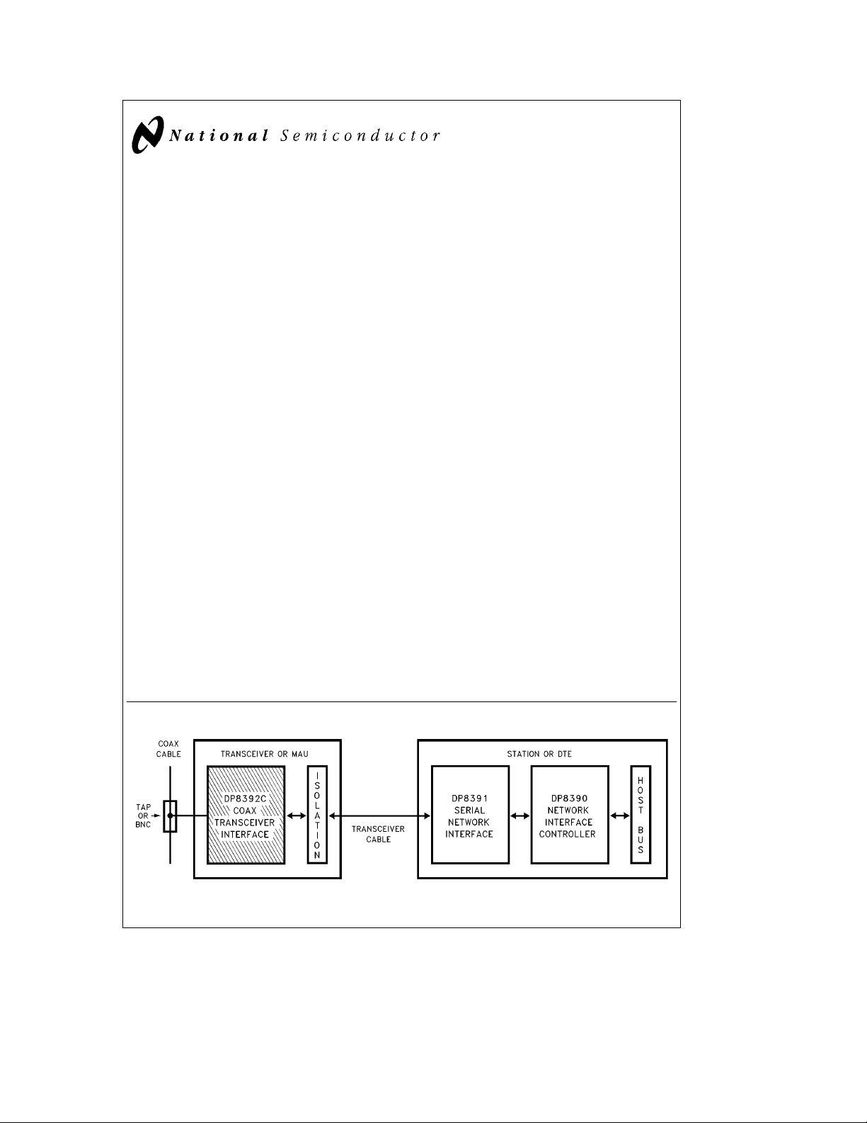
The CTI is part of a three chip set that implements the complete IEEE 802.3 compatible network node electronics as
shown below. The other two chips are the DP8391 Serial
Network Interface (SNI) and the DP8390 Network Interface
Controller (NIC).
The SNI provides the Manchester encoding and decoding
functions; whereas the NIC handles the Media Access Protocol and the buffer management tasks. Isolation between
the CTI and the SNI is an IEEE 802.3 requirement that can
be easily satisfied on signal lines using a set of pulse transformers that come in a standard DIP. However, the power
isolation for the CTI is done by DC-to-DC conversion
through a power transformer.
Features
Y
Compatible with Ethernet II, IEEE 802.3 10Base5 and
10Base2 (Cheapernet)
Y
Integrates all transceiver electronics except signal &
power isolation
Y
Innovative design minimizes external component count
Y
Jabber timer function integrated on chip
Y
Externally selectable CD Heartbeat allows operation
with IEEE 802.3 compatible repeaters
Y
Precision circuitry implements receive mode collision
detection
Y
Squelch circuitry at all inputs rejects noise
Y
Designed for rigorous reliability requirements of
IEEE 802.3
Y
Standard Outline 16-pin DIP uses a special leadframe
that significantly reduces the operating die temperature
Table of Contents
1.0 System Diagram
2.0 Block Diagram
3.0 Functional Description
3.1 Receiver Functions
3.2 Transmitter Functions
3.3 Collision Functions
3.4 Jabber Functions
4.0 Typical Applications
5.0 Connection Diagrams
6.0 Pin Descriptions
7.0 Absolute Maximum Ratings
8.0 DP8392C Electrical Characteristics
9.0 DP8392C-1 Electrical Characteristics
10.0 Switching Characteristics
11.0 Timing and Load Diagram
1.0 System Diagram
IEEE 802.3 Compatible Ethernet/Cheapernet Local Area Network Chip Set
C
1995 National Semiconductor Corporation RRD-B30M115/Printed in U. S. A.
TL/F/11085
TL/F/11085– 1
Page 2
2.0 Block Diagram
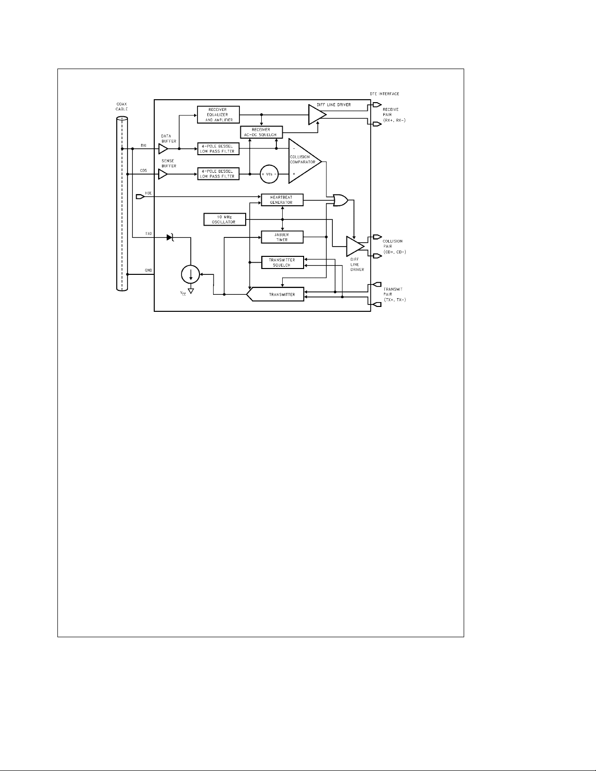
FIGURE 1. DP8392C Block Diagram
3.0 Functional Description
The CTI consists of four main logical blocks:
a) the Receiver - receives data from the coax and sends it
to the DTE
b) the Transmitter - accepts data from the DTE and trans-
mits it onto the coax
c) the Collision Detect circuitry - indicates to the DTE any
collision on the coax
d) the Jabber Timer - disables the Transmitter in case of
longer than legal length packets
3.1 RECEIVER FUNCTIONS
The Receiver includes an input buffer, a cable equalizer, a
4-pole Bessel low pass filter, a squelch circuit, and a differential line driver.
The buffer provides high input impedance and low input capacitance to minimize loading and reflections on the coax.
The equalizer is a high pass filter which compensates for
the low pass effect of the cable. The composite result of the
maximum length cable and the equalizer is a flatband response at the signal frequencies to minimize jitter.
The 4-pole Bessel low pass filter extracts the average DC
level on the coax, which is used by both the Receiver
squelch and the collision detection circuits.
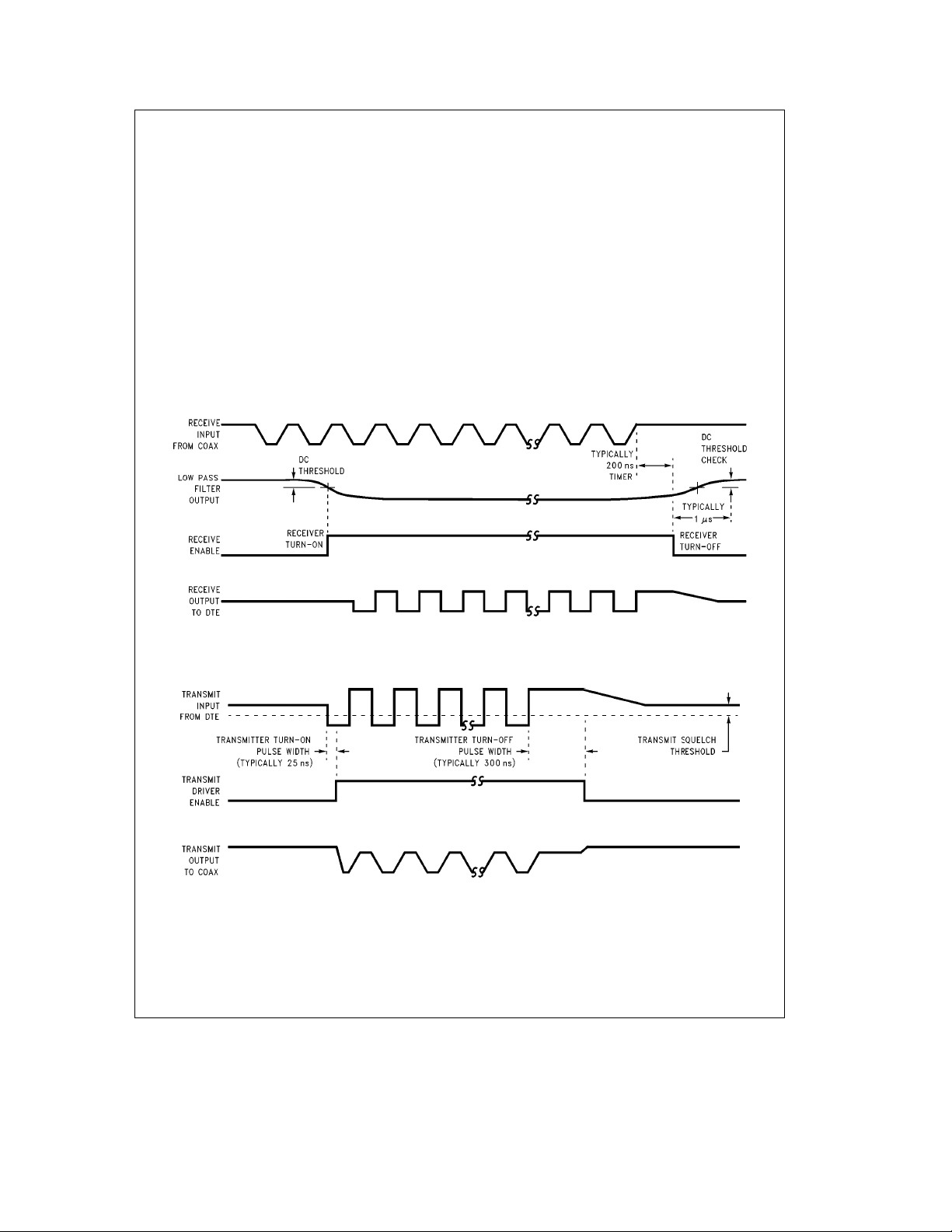
The Receiver squelch circuit prevents noise on the coax
from falsely triggering the Receiver in the absence of the
signal. At the beginning of the packet, the Receiver turns on
when the DC level from the low pass filter is lower than the
DC squelch threshold. However, at the end of the packet, a
quick Receiver turn off is needed to reject dribble bits. This
is accomplished by an AC timing circuit that reacts to high
level signals of greater than typically 200 ns in duration. The
TL/F/11085– 2
Receiver then stays off only if within about 1 ms, the DC
level from the low pass filter rises above the DC squelch
threshold.
The differential line driver provides ECL compatible signals
to the DTE with typically 3 ns rise and fall times. In its idle
state, its outputs go to differential zero to prevent DC standing current in the isolation transformer.
3.2 TRANSMITTER FUNCTIONS
The Transmitter has a differential input and an open collector output current driver. The differential input common
mode voltage is established by the CTI and should not be
altered by external circuitry. The transformer coupling of
TX
802.3/Ethernet Specifications for signal levels. Controlled
rise and fall times (25 ns V
harmonic components. The rise and fall times are matched
to minimize jitter. The drive current levels of the DP8392C
meet the tighter recommended limits of IEEE 802.3 and are
set by a built-in bandgap reference and an external 1% resistor. An on chip isolation diode is provided to reduce the
Transmitter’s coax load capacitance. For Ethernet compatible applications, an external isolation diode (see
may be added to further reduce coax load capacitance. In
Cheapernet compatible applications the external diode is
not required as the coax capacitive loading specifications
are relaxed.
The Transmitter squelch circuit rejects signals with pulse
widths less than typically 20 ns (negative going), or with
levels less than
end of the packet if the signal stays higher than
for more than approximately 300 ns.
Transmitter timing.
Figure 2
illustrates the Receiver timing.
g
will satisfy this condition. The driver meets all IEEE
g
5 ns) minimize the higher
Figure 4
b
175 mV. The Transmitter turns off at the
Figure 3
b
illustrates the
175 mV
)
2
Page 3
3.0 Functional Description (Continued)
3.3 COLLISION FUNCTIONS
The collision circuitry consists of two buffers, two 4-pole
Bessel low pass filters (section 3.1), a comparator, a heartbeat generator, a 10 MHz oscillator, and a differential line
driver.
Two identical buffers and 4-pole Bessel low pass filters extract the DC level on the center conductor (data) and the
shield (sense) of the coax. These levels are monitored by
the comparator. If the data level is more negative than the
sense level by at least the collision threshold (Vth), the collision output is enabled.
At the end of every transmission, the heartbeat generator
creates a pseudo collision for a short time to ensure that the
collision circuitry is properly functioning. This burst on collision output occurs typically 1.1 ms after the transmission,
and has a duration of about 1 ms. This function can be disabled externally with the HBE (Heartbeat Enable) pin to allow operation with repeaters.
The 10 MHz oscillator generates the signal for the collision
and heartbeat functions. It is also used as the timebase for
all the jabber functions. It does not require any external
components.
The collision differential line driver transfers the 10 MHz signal to the CD
g
pair in the event of collision, jabber, or
heartbeat conditions. This line driver also features zero differential idle state.
3.4 JABBER FUNCTIONS
The Jabber Timer monitors the Transmitter and inhibits
transmission if the Transmitter is active for longer than
20 ms (fault). It also enables the collision output for the fault
duration. After the fault is removed, The Jabber Timer waits
for about 500 ms (unjab time) before re-enabling the Transmitter. The transmit input must stay inactive during the unjab
time.
FIGURE 2. Receiver Timing
FIGURE 3. Transmitter Timing
3
TL/F/11085– 3
TL/F/11085– 4
Page 4
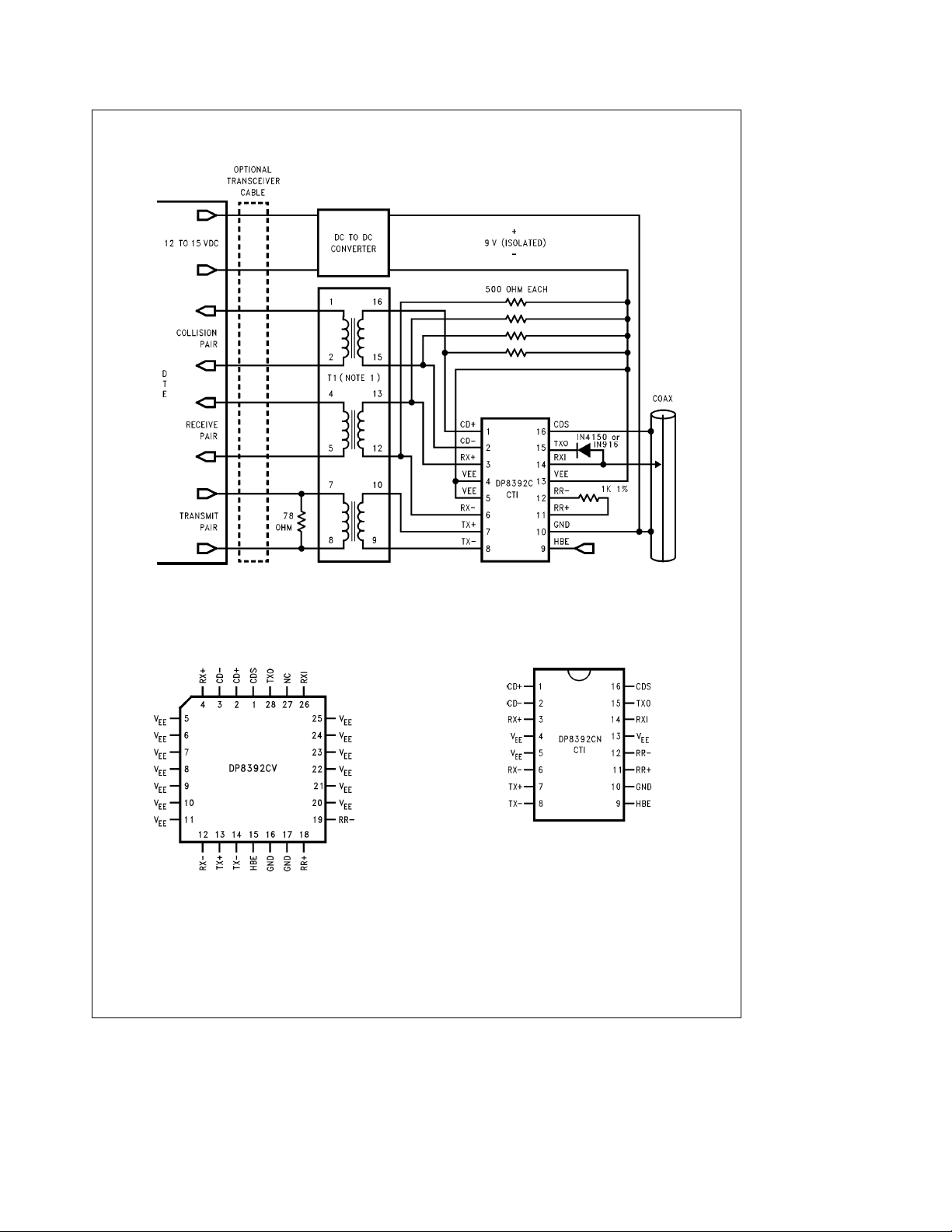
4.0 Typical Application
Note 1: T1 is a 1:1 pulse transformer, Le100 mH
Pulse Engineering (San Diego) Part No. 64103
Valor Electronics (San Diego) Part No.
LT6003 or equivalent
5.0 Connection Diagrams
Order Number DP8392CV
See NS Package Number V28A
TL/F/11085– 6
FIGURE 4
TL/F/11085– 5
TL/F/11085– 16
Top View
Order Number DP8392CN
See NS Package Number N16E
FIGURE 5
4
Page 5

6.0 Pin Descriptions
28-Pin PLCC 16-Pin DIP Name I/O Description
*
21CD
32CD
43RX
12 6 RX
13 7 TX
14 8 TX
15 9 HBE I Heartbeat Enable. This input enables CD Heartbeat when grounded, disables it
18 11 RR
19 12 RR
26 14 RXI I Receive Input. Connects directly to the coaxial cable. Signals meeting Receiver
28 15 TXO O Transmit Output. Connects either directly (Cheapernet) or via an isolation diode
1 16 CDS I Collision Detect Sense. Ground sense connection for the collision detect circuit.
16, 17 10 GND Positive Supply Pin. A 0.1 mF ceramic decoupling capacitor must be connected
5–11 4 VEE Negative Supply Pins. In order to make full use of the 3.5W power dissipation
20–25 5
13
e
*IEEE names for CD
g
CIg,RX
6.1 P.C. BOARD LAYOUT
The DP8392C package is uniquely designed to ensure that
the device meets the 1 million hour Mean Time Between
Failure (MTBF) requirement of the IEEE 802.3 standard. In
order to fully utilize this heat dissipation design, the three
V
pins are to be connected to a copper plane which
EE
should be included in the printed circuit board layout.
There are two basic considerations in designing a PCB for
the DP8392C and C-1 CTI. The first is ensuring that the
layout does not degrade the electrical characteristics of the
DP8392, and enables the end product to meet the IEEE
802.3 specifications. The second consideration is meeting
the thermal requirements to the DP8392.
Since the DP8392 is highly integrated the layout is actually
quite simple, and there are just a few guidelines:
1. Ensure that the parasitic capacitance added to the RXI
and TXO pins is minimized. To do this keep these signal
traces short, and remove any power planes under these
signals, and under any components that connect to these
signals.
Figure 6
shows the component placement for the
DIP package. The PLCC component placement would be
similar, as shown in
Figure 7
a
b
*
a
b
*
a
b
a
b
e
g
DIg,TX
.
OCollision Output. Balanced differential line driver outputs from the collision detect
circuitry. The 10 MHz signal from the internal oscillator is transferred to these
outputs in the event of collision, excessive transmission (jabber), or during CD
Heartbeat condition. These outputs are open emitters; pulldown resistors to VEE
are required. When operating into a 78X transmission line, these resistors should
be 500X. In Cheapernet applications, where the 78X drop cable is not used,
higher resistor values (up to 1.5k) may be used to save power.
OReceive Output. Balanced differential line driver outputs from the Receiver. These
outputs also require 500X pulldown resistors.
I Transmit Input. Balanced differential line receiver inputs to the Transmitter. The
common mode voltage for these inputs is determined internally and must not be
externally established. Signals meeting Transmitter squelch requirements are
waveshaped and output at TXO.
when connected to VEE.
I External Resistor. A fixed 1k 1% resistor connected between these pins
establishes internal operating currents.
squelch requirements are equalized for inter-symbol distortion, amplified, and
outputted at RX
g
.
(Ethernet) to the coaxial cable.
This pin should be connected separately to the shield to avoid ground drops from
altering the receive mode collision threshold.
across GND and VEE as close to the device as possible.
capability of this package, these pins should be connected to a large metal frame
area on the PC board. Doing this will reduce the operating die temperature of the
device thereby increasing the long term reliability.
e
g
g
DO
2. The power supply layout to the CTI should be relatively
clean. Usually the CTI’s power is supplied directly by a
DC-DC converter. The power should be routed either
through separate isolated planes, or via thick PCB traces.
For the second consideration, the packaged DP8392 must
have a thermal resistance of 40
0
C–70§C temperature range. The CTI dissipates more
§
power when transmitting than while it is idle. In order to do
C–45§C/W to meet the full
§
this the thermal resistance of the device must be 40
45
C/W. To meet this requirement during transmission, it is
§
recommended that a small printed circuit board plane be
connected to all V
pins on the solder side of the PCB.
EE
The size of the trace plane depends on the package used
and the duty cycle of transmissions. For the DIP package
the plane should be connected to pins 4– 5, 13, and the size
should be approximately 0.2 square inches for applications
where the duty cycle of the transmitter is very low (
This would be typical of adapter or motherboard applications. In applications where the transmitter duty cycle may
be large (repeaters and external transceivers) the total area
should be increased to 0.4 in
2
.
Figure 6
illustrates a recom-
mended component side layout for these planes.
k
C–
§
10%).
5
Page 6

6.0 Pin Descriptions (Continued)
For the PLCC packaged DP8392, it is recommended that a
small printed circuit board V
5–11, and a second one be connected to pins 20 – 25. To
reduce the thermal resistance to the required value, the
area of the plane on EACH set of pins should be
for applications with low transmitter duty cycle, andt0.4 in
for high transmit duty cycle applications.
a recommended component side layout for these planes.
plane be connected to pins
EE
t
Figure 7
illustrates
0.20 in
2
2
Layout as viewed from component side
FIGURE 6. Typical Layout Considerations
for DP8392CN
(Not to Scale)
FIGURE 7. Recommended Layout and Dissipation Planes for DP8392CV (Not to Scale)
TL/F/11085– 14
TL/F/11085– 15
6
Page 7

7.0 Absolute Maximum Ratings (Note 1)
b
65§to 150§C
b
12V
Supply Voltage (V
)
EE
Package Power Rating at 25§C 3.5 Watts*
(PC Board Mounted) See Section 5
Derate linearly at the rate of 28.6 mW/
C
§
Input Voltage 0 tob12V
Storage Temperature
Lead Temp. (Soldering, 10 seconds) 260§C
*For actual power dissipation of the device please refer to section 7.0.
Recommended Operating
Conditions
Supply Voltage (VEE)
Ambient Temperature 0§to 70§C
If Military/Aerospace specified devices are required,
please contact the National Semiconductor Sales
Office/Distributors for availability and specifications.
b
9vg5%
8.0 DP8392C Electrical Characteristics V
All parameters with respect to CD
g
and RXgare measured after the pulse transformer except VOC.
EE
eb
9Vg5%, T
e
0§to 70§C (Notes2&3)
A
Symbol Parameter Min Typ Max Units
I
EE1
I
EE2
I
RXI
I
TDC
I
TAC
V
V
V
V
V
C
R
R
CD
OD
OC
OB
TS
X
RXI
TXO
Supply current out of VEEpinÐnon transmitting
Supply current out of VEEpinÐtransmitting
Receive input bias current (RXI)
Transmit output dc current level (TXO) 37 41 45 mA
Transmit output ac current level (TXO)
Collision threshold (Receive mode)
Differential output voltage (RXg,CDg)
Common mode output voltage (RXg,CDg)
Diff. output voltage imbalance (RXg,CDg)
Transmitter squelch threshold (TXg)
Input capacitance (RXI) 1.2 pF
Shunt resistanceÐnon transmitting (RXI) 100 KX
Shunt resistanceÐtransmitting (TXO) 10 KX
9.0 DP8392C-1 Electrical Characteristics V
All parameters with respect to CD
g
and RXgare measured after the pulse transformer except VOC.
b
2
g
28 I
b
1.45
g
550
b
1.5
b
175
eb
9Vg5%, T
EE
b
85
b
125
b
1.53
b
2.0
b
225
e
0§to 70§C (Notes2&3)
A
b
130 mA
b
180 mA
a
25 mA
TDC
b
1.58 V
g
1200 mV
b
2.5 V
g
40 mV
b
300 mV
mA
Symbol Parameter Min Typ Max Units
I
EE1
I
EE2
I
RXI
I
TDC
I
TAC
V
CD
V
OD
V
OC
V
OB
V
TS
C
X
R
RXI
R
TXO
Note 1: Absolute maximum ratings are those values beyond which the safety of the device cannot be guaranteed. They are not meant to imply that the device
should be operated at these limits.
Note 2: All currents into device pins are positive, all currents out of device pins are negative. All voltages referenced to ground unless otherwise specified.
Note 3: All typicals are given for V
Supply current out of VEEpinÐnon transmitting
Supply current out of VEEpinÐtransmitting
Receive input bias current (RXI)
b
2
Transmit output dc current level (TXO) 37 41 45 mA
Transmit output ac current level (TXO)
Collision threshold (Receive mode)
Differential output voltage (RXg,CDg)
Common mode output voltage (RXg,CDg)
g
28 I
b
1.45
g
550
b
1.5
Diff. output voltage imbalance (RXg,CDg)
Transmitter squelch threshold (TXg)
b
175
Input capacitance (RXI) 1.2 pF
Shunt resistanceÐnon transmitting (RXI) 100 KX
Shunt resistanceÐtransmitting (TXO) 7.5K 10 KX
eb
EE
9V and T
e
25§C.
A
b
85
b
125
b
1.53
b
2.0
b
225
b
130 mA
b
180 mA
a
25 mA
TDC
b
1.58 V
g
1200 mV
b
2.5 V
g
40 mV
b
275 mV
mA
7
Page 8

10.0 DP8392C Switching Characteristics V
EE
eb
9Vg5%, T
e
0§to 70§C (Note 3)
A
Symbol Parameter Fig Min Typ Max Units
t
RON
t
Rd
t
Rr
t
Rf
t
RJ
t
TST
t
Td
t
Tr
t
Tf
t
TM
t
TS
t
TON
t
TOFF
t
CON
t
COFF
f
CD
t
CP
t
HON
t
HW
t
JA
t
JR
Receiver startup delay (RXI to RXg) 8 & 14 4 bits
Receiver propagation delay (RXI to RXg) 8&14 15 50 ns
Differential outputs rise time (RXg,CDg) 8&14 4 ns
Differential outputs fall time (RXg,CDg) 8&14 4 ns
Receiver & cable total jitter 13
g
2ns
Transmitter startup delay (TXgto TXO) 9 & 14 1 bits
Transmitter propagation delay (TXgto TXO) 9 & 14 25 50 ns
Transmitter rise time Ð10% to 90% (TXO) 9 & 14 25 ns
Transmitter fall time Ð90% to 10% (TXO) 9 & 14 25 ns
tTrand tTfmismatch 0.5 ns
Transmitter skew (TXO)
g
0.5 ns
Transmit turn-on pulse width at VTS(TXg) 9&14 20 ns
Transmit turn-off pulse width at VTS(TXg) 9 & 14 250 ns
Collision turn-on delay 10 & 14 7 bits
Collision turn-off delay 10 & 14 20 bits
Collision frequency (CDg) 10 & 14 8.0 12.5 MHz
Collision pulse width (CDg) 10&14 35 70 ns
CD Heartbeat delay (TXgto CDg) 11 & 14 0.6 1.6 ms
CD Heartbeat duration (CDg) 11 & 14 0.5 1.0 1.5 ms
Jabber activation delay (TXgto TXO and CDg) 12&14 20 29 60 ms
Jabber reset unjab time (TXgto TXO and CDg) 12 & 14 250 500 750 ms
DP8392C-1 Switching Characteristics V
EE
eb
9Vg5%, T
e
0§to 70§C (Note 3)
A
Symbol Parameter Fig Min Typ Max Units
t
RON
t
Rd
t
Rr
t
Rf
t
RJ
t
TST
t
Td
t
Tr
t
Tf
t
TM
t
TS
t
TON
t
TOFF
t
CON
t
COFF
f
CD
t
CP
t
HON
t
HW
t
JA
t
JR
Note 1: Absolute maximum ratings are those values beyond which the safety of the device cannot be guaranteed. They are not meant to imply that the device
should be operated at these limits.
Note 2: All currents into device pins are positive, all currents out of device pins are negative. All voltages referenced to ground unless otherwise specified.
Note 3: All typicals are given for V
Receiver startup delay (RXI to RXg) 8 & 14 4 5 bits
Receiver propagation delay (RXI to RXg) 8&14 15 50 ns
Differential outputs rise time (RXg,CDg) 8&14 4 7 ns
Differential outputs fall time (RXg,CDg) 8&14 4 7 ns
Receiver & cable total jitter 13
g
2ns
Transmitter startup delay (TXgto TXO) 9 & 14 1 2 bits
Transmitter propagation delay (TXgto TXO) 9 & 14 5 25 50 ns
Transmitter rise time Ð10% to 90% (TXO) 9 & 14 20 25 30 ns
Transmitter fall time Ð90% to 10% (TXO) 9 & 14 20 25 30 ns
tTrand tTfmismatch 0.5 ns
Transmitter skew (TXO)
g
0.5 ns
Transmit turn-on pulse width at VTS(TXg) 9 & 14 5 20 40 ns
Transmit turn-off pulse width at VTS(TXg) 9 & 14 110 270 ns
Collision turn-on delay 10 & 14 7 13 bits
Collision turn-off delay 10 & 14 20 bits
Collision frequency (CDg) 10 & 14 8.5 12.5 MHz
Collision pulse width (CDg) 10&14 35 70 ns
CD Heartbeat delay (TXgto CDg) 11 & 14 0.6 1.6 ms
CD Heartbeat duration (CDg) 11 & 14 0.5 1.0 1.5 ms
Jabber activation delay (TXgto TXO and CDg) 12&14 20 29 60 ms
Jabber reset unjab time (TXgto TXO and CDg) 12 & 14 250 500 750 ms
eb
EE
9V and T
e
25§C.
A
8
Page 9

11.0 Timing and Load Diagrams
FIGURE 8. Receiver Timing
FIGURE 9. Transmitter Timing
FIGURE 10. Collision Timing
TL/F/11085– 7
TL/F/11085– 8
TL/F/11085– 9
FIGURE 11. Heartbeat Timing
9
TL/F/11085– 10
Page 10

11.0 Timing and Load Diagrams (Continued)
FIGURE 12. Jabber Timing
Receiver equalization (jitter correction)t1ns
Input jitter at RX
Output jitter at RX
gsg
7ns TL/F/11085– 12
gsg
6ns
FIGURE 13. Receive Jitter Timing
TL/F/11085– 11
*The 50 mH inductance is for testing purposes. Pulse transformers with higher inductances are recommended (see
TL/F/11085– 13
FIGURE 14. Test Loads
10
Figure 4
)
Page 11

12.0 Physical Dimensions inches (millimeters)
Molded Dual-In-Line Package (N)
Order Number DP8392CN or DP8392CN-1
NS Package Number N16E
11
Page 12

12.0 Physical Dimensions inches (millimeters) (Continued) Lit.
Ý
103054
DP8392C/DP8392C-1 CTI Coaxial Transceiver Interface
28-Lead Plastic Chip Carrier
Order Number DP8392CV or DP8392CV-1
NS Package Number V28A
LIFE SUPPORT POLICY
NATIONAL’S PRODUCTS ARE NOT AUTHORIZED FOR USE AS CRITICAL COMPONENTS IN LIFE SUPPORT
DEVICES OR SYSTEMS WITHOUT THE EXPRESS WRITTEN APPROVAL OF THE PRESIDENT OF NATIONAL
SEMICONDUCTOR CORPORATION. As used herein:
1. Life support devices or systems are devices or 2. A critical component is any component of a life
systems which, (a) are intended for surgical implant support device or system whose failure to perform can
into the body, or (b) support or sustain life, and whose be reasonably expected to cause the failure of the life
failure to perform, when properly used in accordance support device or system, or to affect its safety or
with instructions for use provided in the labeling, can effectiveness.
be reasonably expected to result in a significant injury
to the user.
National Semiconductor National Semiconductor National Semiconductor National Semiconductor
Corporation Europe Hong Kong Ltd. Japan Ltd.
1111 West Bardin Road Fax: (
Arlington, TX 76017 Email: cnjwge@tevm2.nsc.com Ocean Centre, 5 Canton Rd. Fax: 81-043-299-2408
Tel: 1(800) 272-9959 Deutsch Tel: (
Fax: 1(800) 737-7018 English Tel: (
National does not assume any responsibility for use of any circuitry described, no circuit patent licenses are implied and National reserves the right at any time without notice to change said circuitry and specifications.
Fran3ais Tel: (
Italiano Tel: (
a
49) 0-180-530 85 86 13th Floor, Straight Block, Tel: 81-043-299-2309
a
49) 0-180-530 85 85 Tsimshatsui, Kowloon
a
49) 0-180-532 78 32 Hong Kong
a
49) 0-180-532 93 58 Tel: (852) 2737-1600
a
49) 0-180-534 16 80 Fax: (852) 2736-9960
 Loading...