

Page 1
TL/F/9357
DP8391A/NS32491A SNI Serial Network Interface
July 1993
DP8391A/NS32491A SNI Serial Network Interface
General Description
The DP8391A Serial Network Interface (SNI) provides the
Manchester data encoding and decoding functions for
IEEE 802.3 Ethernet/Cheapernet type local area networks.
The SNI interfaces the DP8390 Network Interface Controller
(NIC) to the Ethernet transceiver cable. When transmitting,
the SNI converts non-return-to-zero (NRZ) data from the
controller and clock pulses into Manchester encoding and
sends the converted data differentially to the transceiver.
The opposite process occurs on the receive path, where a
digital phase-locked loop decodes 10 Mbit/s signals with as
much as
g
18 ns of jitter.
The DP8391A SNI is a functionally complete Manchester
encoder/decoder including ECL like balanced driver and receivers, on board crystal oscillator, collision signal translator, and a diagnostic loopback circuit.
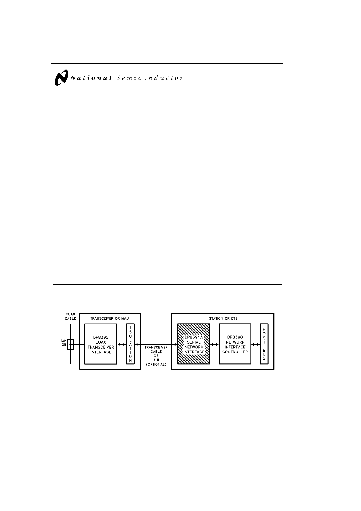
The SNI is part of a three chip set that implements the complete IEEE compatible network node electronics as shown
below. The other two chips are the DP8392 Coax Transceiver Interface (CTI) and the DP8390 Network Interface Controller (NIC).
Incorporated into the CTI are the transceiver, collision and
jabber functions. The Media Access Protocol and the buffer
management tasks are performed by the NIC. There is an
isolation requirement on signal and power lines between the
CTI and the SNI. This is usually accomplished by using a set
of miniature pulse transformers that come in a 16-pin plastic
DIP for signal lines. Power isolation, however, is done by
using a DC to DC converter.
Features
Y
Compatible with Ethernet II, IEEE 802.3; 10Base5,
10Base2, and 10Base-T
Y
10 Mb/s Manchester encoding/decoding with receive
clock recovery
Y
Patented digital phase locked loop (DPLL) decoder requires no precision external components
Y
Decodes Manchester data with up tog18 ns of jitter
Y
Loopback capability for diagnostics
Y
Externally selectable half or full step modes of operation at transmit output
Y
Squelch circuits at the receive and collision inputs reject noise
Y
High voltage protection at transceiver interface (16V)
Y
TTL/MOS compatible controller interface
Y
Connects directly to the transceiver (AUI) cable
Table of Contents
1.0 System Diagram
2.0 Block Diagram
3.0 Functional Description
3.1 Oscillator
3.2 Encoder
3.3 Decoder
3.4 Collision Translator
3.5 Loopback
4.0 Connection Diagrams
5.0 Pin Descriptions
6.0 Absolute Maximum Ratings
7.0 Electrical Characteristics
8.0 Switching Characteristics
9.0 Timing and Load Diagrams
10.0 Physical Dimensions
1.0 System Diagram
IEEE 802.3 Compatible Ethernet/Cheapernet Local Area Network Chip Set
TL/F/9357– 1
C
1995 National Semiconductor Corporation RRD-B30M105/Printed in U. S. A.
Page 2
2.0 Block Diagram
TL/F/9357– 2
FIGURE 1
3.0 Functional Description
The SNI consists of five main logical blocks:
a) the oscillatorÐgenerates the 10 MHz transmit clock sig-
nal for system timing.
b) the Manchester encoder and differential output driverÐ
accepts NRZ data from the controller, performs Manchester encoding, and transmits it differentially to the
transceiver.
c) the Manchester decoderÐreceives Manchester data
from the transceiver, converts it to NRZ data and clock
pulses, and sends them to the controller.
d) the collision translatorÐindicates to the controller the
presence of a valid 10 MHz signal at its input.
e) the loopback circuitryÐwhen asserted, switches encod-
ed data instead of receive input signals to the digital
phase-locked loop.
3.1 OSCILLATOR
The oscillator is controlled by a 20 MHz parallel resonant
crystal connected between X1 and X2 or by an external
clock on X1. The 20 MHz output of the oscillator is divided
by 2 to generate the 10 MHz transmit clock for the controller. The oscillator also provides internal clock signals to the
encoding and decoding circuits.
Crystal Specification
Resonant frequency 20 MHz
Tolerance
g
0.001% at 25§C
Stability
g
0.005% 0–70§C
Type AT-Cut
Circuit Parallel Resonance
The 20 MHz crystal connection to the SNI requires special
care. The IEEE 802.3 standard requires a 0.01% absolute
accuracy on the transmitted signal frequency. Stray capacitance can shift the crystal’s frequency out of range, causing
the transmitted frequency to exceed its 0.01% tolerance.
The frequency marked on the crystal is usually measured
with a fixed shunt capacitance (C
L
) that is specified in the
crystal’s data sheet. This capacitance for 20 MHz crystals is
typically 20 pF. The capacitance between the X1 and X2
pins of the SNI, of the PC board traces and the plated
through holes plus any stray capacitance such as the socket capacitance, if one is used, should be estimated or measured. Once the total sum of these capacitances is determined, the value of additional external shunt capacitance
required can be calculated. This capacitor can be a fixed
5% tolerance component. The frequency accuracy should
be measured during the design phase at the transmit clock
pin (TXC) for a given pc layout.
Figure 2
shows the crystal
connection.
TL/F/9357– 3
CLeLoad capacitance specified by the crystal’s manufacturer
CP
e
Total parasitic capacitance including:
a) SNI input capacitance between X1 and X2 (typically 5 pF)
b) PC board traces, plated through holes, socket capacitances
Note 1: When using a Viking (San Jose) VXB49N5 crystal, the external ca-
pacitor is not required, as the C
L
of the crystal matches the input
capacitance of the DP8391A.
FIGURE 2. Crystal Connection
3.2 MANCHESTER ENCODER AND DIFFERENTIAL
DRIVER
The encoder combines clock and data information for the
transceiver. Data encoding and transmission begins with the
transmit enable input (TXE) going high. As long as TXE re-
2
Page 3

3.0 Functional Description (Continued)
mains high, transmit data (TXD) is encoded out to the transmit-driver pair (TX
g
). The transmit enable and transmit data
inputs must meet the setup and hold time requirements with
respect to the rising edge of transmit clock. Transmission
ends with the transmit enable input going low. The last transition is always positive at the transmit output pair. It will
occur at the center of the bit cell if the last bit is one, or at
the boundary of the bit cell if the last bit is zero.
The differential line driver provides ECL like signals to the
transceiver with typically 5 ns rise and fall times. It can drive
up to 50 meters of twisted pair AUI Ethernet transceiver
cable. These outputs are source followers which need external 270X pulldown resistors to ground. Two different
modes, full-step or half-step, can be selected with SEL input. With SEL low, transmit
a
is positive with respect to
transmit
b
in the idle state. With SEL high, transmitaand
transmit
b
are equal in the idle state, providing zero differ-
ential voltage to operate with transformer coupled loads.
Figures 4, 5
and6illustrate the transmit timing.
3.3 MANCHESTER DECODER
The decoder consists of a differential input circuitry and a
digital phase-locked loop to separate Manchester encoded
data stream into clock signals and NRZ data. The differential input should be externally terminated if the standard
78X transceiver drop cable is used. Two 39X resistors connected in series and one optional common mode bypass
capacitor would accomplish this. A squelch circuit at the
input rejects signals with pulse widths less than 5 ns (negative going), or with levels less than
b
175 mV. Signals more
negative than
b
300 mV and with a duration greater than
30 ns are always decoded. This prevents noise at the input
from falsely triggering the decoder in the absence of a valid
signal. Once the input exceeds the squelch requirements,
carrier sense (CRS) is asserted. Receive data (RXD) and
receive clock (RXC) become available typically within 6 bit
times. At this point the digital phase-locked loop has locked
to the incoming signal. The DP8391A decodes a data frame
with up to
g
18 ns of jitter correctly.
The decoder detects the end of a frame when the normal
mid-bit transition on the differential input ceases. Within one
and a half bit times after the last bit, carrier sense is de-asserted. Receive clock stays active for five more bit times
before it goes low and remains low until the next frame.
Figures 7, 8
and9illustrate the receive timing.
3.4 COLLISION TRANSLATOR
The Ethernet transceiver detects collisions on the coax cable and generates a 10 MHz signal on the transceiver cable.
The SNI’s collision translator asserts the collision detect
output (COL) to the DP8390 controller when a 10 MHz signal is present at the collision inputs. The controller uses this
signal to back off transmission and recycle itself. The collision detect output is de-asserted within 350 ns after the 10
MHz input signal disappears.
The collision differential inputs (
a
andb) should be terminated in exactly the same way as the receive inputs. The
collision input also has a squelch circuit that rejects signals
with pulse widths less than 5 ns (negative going), or with
levels less than
b
175 mV.
Figure 10
illustrates the collision
timing.
3.5 LOOPBACK FUNCTIONS
Logic high at loopback input (LBK) causes the SNI to route
serial data from the transmit data input, through its encoder,
returning it through the phase-locked-loop decoder to receive data output. In loopback mode, the transmit driver is in
idle state and the receive and collision input circuitries are
disabled.
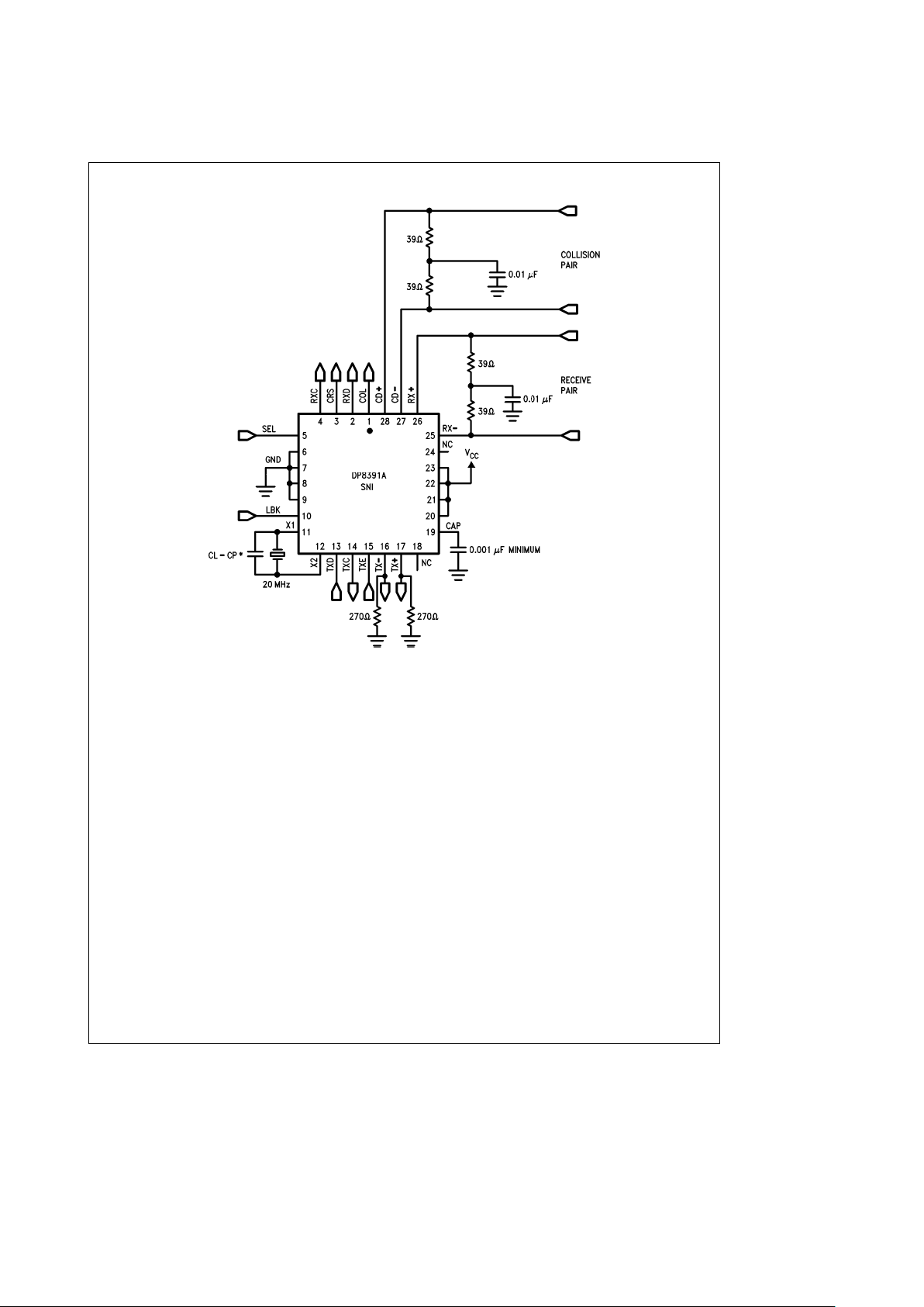
4.0 Connection Diagram
Top View
*Refer to the Oscillator section TL/F/9357– 4
FIGURE 3a
Order Number DP8391AN
See NS Package Number N24C
3
Page 4
PCC Connection Diagram
TL/F/9357– 5
*Refer to the Oscillator section
FIGURE 3b
Order Number DP8391AV
NS Package Number V28A
4
Page 5

5.0 Pin Descriptions
Pin No.
Name I/O Description
(DIP) (PCC)
1 1 COL O Collision Detect Output. A TTL/MOS level active high output. A 10 MHz
(
a
25%–15%) signal at the collision input will produce a logic high at COL
output. When no signal is present at the collision input, COL output will go low.
2 2 RXD O Receive Data Output. A TTL/MOS level signal. This is the NRZ data output
from the digital phase-locked loop. This signal should be sampled by the
controller at the rising edge of receive clock.
3 3 CRS O Carrier Sense. A TTL/MOS level active high signal. It is asserted when valid
data from the transceiver is present at the receive input. It is de-asserted one
and a half bit times after the last bit at receive input.
4 4 RXC O Receive Clock. A TTL/MOS level recovered clock. When the phase-locked loop
locks to a valid incoming signal a 10 MHz clock signal is activated on this output.
This output remains low during idle (5 bit times after activity ceases at receive
input).
5 5 SEL I Mode Select. A TTL level input. When high, transmitaand transmitboutputs
are at the same voltage in idle state providing a ‘‘zero’’ differential. When low,
transmit
a
is positive with respect to transmitbin idle state.
6 6–9 GND Negative Supply Pins.
7 10 LBK I Loopback. A TTL level active high on this input enables the loopback mode.
811X1 ICrystal or External Frequency Source Input (TTL).
912X2 OCrystal Feedback Output. This output is used in the crystal connection only. It
must be left open when driving X1 with an external frequency source.
10 13 TXD I Transmit Data. A TTL level input. This signal is sampled by the SNI at the rising
edge of transmit clock when transmit enable input is high. The SNI combines
transmit data and transmit clock signals into a Manchester encoded bit stream
and sends it differentially to the transceiver.
11 14 TXC O Transmit Clock. A TTL/MOS level 10 MHz clock signal derived from the 20
MHz oscillator. This clock signal is always active.
12 15 TXE I Transmit Enable. A TTL level active high data encoder enable input. This signal
is also sampled by the SNI at the rising edge of transmit clock.
13 16 TX
b
O Transmit Output. Differential line driver which sends the encoded data to the
transceiver. These outputs are source followers and require 270X pulldown
14 17 TX
a
resistors to GND.
15 18 NC No Connection.
16
17 19 CAP O Bypass Capacitor. A ceramic capacitor (greater than 0.001 mF) must be
connected from this pin to GND.
18 20– 23 VCC Positive Supply Pins. A 0.1 mF ceramic decoupling capacitor must be
connected across VCC and GND as close to the device as possible.
19
20 24 NC No Connection.
21 25 RX
b
I Receive Input. Differential receive input pair from the transceiver.
22 26 RX
a
23 27 CD
b
I Collision Input. Differential collision input pair from the transceiver.
24 28 CD
a
5
Page 6

6.0 Absolute Maximum Ratings
Supply Voltage (VCC)7V
Input Voltage (TTL) 0 to 5.5V
Input Voltage (differential)
b
5.5 toa16V
Output Voltage (differential) 0 to 16V
Output Current (differential)
b
40 mA
Storage Temperature
b
65§to 150§C
Lead Temperature (soldering, 10 sec) 300§C
Package Power Rating for DIP at 25§C 2.95W*
(PC Board Mounted)
Derate Linearly at the rate of 23.8 mW/
§
C
Package Power Rating for PCC at 25§C 1.92W*
Derate Linearly at the rate of 15.4 mW/
§
C
*For actual power dissipation of the device please refer to
Section 7.0.
ESD rating 2000V
Recommended Operating
Conditions
Supply Voltage (VCC)5V
g
5%
Ambient Temperature (DIP) 0§to 70§C
(PCC) 0
§
to 55§C
Note:
Absolute maximum ratings are those values beyond
which the safety of the device cannot be guaranteed. They
are not meant to imply that the device should be operated at
these limits.
7.0 Electrical Characteristics
V
CC
e
5Vg5%, T
A
e
0§Cto70§C for DIP and 0§Cto55§C for PCC (Notes1&2)
Symbol Parameter Test Conditions Min Max Units
V
IH
Input High Voltage (TTL) 2.0 V
V
IHX1a
Input High Voltage (X1) No Series Resistor 2.0 V
CC
b
1.5 V
V
IHX1b
Input High Voltage (X1) 1k Series Resistor 2.0 V
CC
V
V
IL
Input Low Voltage (TTL and X1) 0.8 V
I
IH
Input High Current (TTL) V
IN
e
V
CC
50 mA
Input High Current (RX
gCDg
)V
IN
e
V
CC
500 mA
I
IL
Input Low Current (TTL) V
IN
e
0.5V
b
300 mA
Input Low Current (RX
gCDg
)V
IN
e
0.5V
b
700 mA
V
CL
Input Clamp Voltage (TTL) I
IN
eb
12 mA
b
1.2 V
V
OH
Ouptut High Voltage (TTL/MOS) I
OH
eb
100 mA 3.5 V
V
OL
Output Low Voltage (TTL/MOS) I
OL
e
8 mA 0.5 V
I
OS
Output Short Circuit Current (TTL/MOS)
b
40
b
200 mA
V
OD
Differential Output Voltage (TXg)78Xtermination, and
g
550
g
1200 mV
270X from each to GND
V
OB
Diff. Output Voltage Imbalance (TXg) same as above
g
40 mV
V
DS
Diff. Squelch Threshold (RXgCDg)
b
175
b
300 mV
V
CM
Diff. Input Common Mode Voltage (RXgCDg)
b
5.25 5.25 V
I
CC
Power Supply Current 10Mbit/s 270 mA
8.0 Switching Characteristics V
CC
e
5Vg5%, T
A
e
0§Cto70§C for DIP and 0§Cto55§C for PCC (Note 2)
Symbol Parameter Figure Min Typ Max Units
OSCILLATOR SPECIFICATION
t
XTH
X1 to Transmit Clock High 12 8 20 ns
t
XTL
X1 to Transmit Clock Low 12 8 20 ns
TRANSMIT SPECIFICATION
t
TCd
Transmit Clock Duty Cycle at 50% (10 MHz) 12 42 50 58 %
t
TCr
Transmit Clock Rise Time (20% to 80%) 12 8 ns
t
TCf
Transmit Clock Fall Time (80% to 20%) 12 8 ns
t
TDs
Transmit Data Setup Time to Transmit Clock Rising Edge 4 & 12 20 ns
t
TDh
Transmit Data Hold Time from Transmit Clock Rising Edge 4 & 12 0 ns
t
TEs
Transmit Enable Setup Time to Trans. Clock Rising Edge 4 & 12 20 ns
t
TEh
Transmit Enable Hold Time from Trans. Clock Rising Edge 5 & 12 0 ns
Note 1: All currents into device pins are positive, all currents out of device pins are negative. All voltages are referenced to ground unless otherwise specified.
Note 2: All typicals are given for V
CC
e
5V and T
A
e
25§C.
6
Page 7

8.0 Switching Characteristics
V
CC
e
5Vg5%, T
A
e
0§Cto70§C for DIP and 0§Cto55§C for PCC (Note 2) (Continued)
Symbol Parameter Figure Min Typ Max Units
TRANSMIT SPECIFICATION (Continued)
t
TOd
Transmit Output Delay from Transmit Clock Rising Edge 4 & 12 50 ns
t
TOr
Transmit Output Rise Time (20% to 80%) 12 7 ns
t
TOf
Transmit Output Fall Time (80% to 20%) 12 7 ns
t
TOj
Transmit Output Jitter 12
g
0.25 ns
t
TOh
Transmit Output High Before Idle in Half Step Mode 5 & 12 200 ns
t
TOi
Transmit Output Idle Time in Half Step Mode 5 & 12 800 ns
RECEIVE SPECIFICATION
t
RCd
Receive Clock Duty Cycle at 50% (10 MHz) 12 40 50 60 %
t
RCr
Receive Clock Rise Time (20% to 80%) 12 8 ns
t
RCf
Receive Clock Fall Time (80% to 20%) 12 8 ns
t
RDr
Receive Data Rise Time (20% to 80%) 12 8 ns
t
RDf
Receive Data Fall Time (80% to 20%) 12 8 ns
t
RDs
Receive Data Stable from Receive Clock Rising Edge 7 & 12
g
40 ns
t
CSon
Carrier Sense Turn On Delay 7 & 12 50 ns
t
CSoff
Carrier Sense Turn Off Delay 8,9&12 160 ns
t
DAT
Decoder Acquisition Time 7 0.6 1.80 m s
t
Drej
Differential Inputs Rejection Pulse Width (Squelch) 7 5 30 ns
t
Rd
Receive Throughput Delay 8 & 12 150 ns
COLLISION SPECIFICATION
t
COLon
Collision Turn On Delay 10 & 12 50 ns
t
COLoff
Collision Turn Off Delay 10 & 12 350 ns
LOOPBACK SPECIFICATION
t
LBs
Loopback Setup Time 11 20 ns
t
LBh
Loopback Hold Time 11 0 ns
Note 2: All typicals are given for V
CC
e
5V and T
A
e
25§C.
9.0 Timing and Load Diagrams
TL/F/9357– 6
FIGURE 4. Transmit Timing - Start of Transmission
7
Page 8

9.0 Timing and Load Diagrams (Continued)
TL/F/9357– 7
FIGURE 5. Transmit Timing - End of Transmission (last bite0)
TL/F/9357– 8
FIGURE 6. Transmit Timing - End of Transmission (last bite1)
8
Page 9

9.0 Timing and Load Diagrams (Continued)
TL/F/9357– 9
FIGURE 7. Receive Timing - Start of Packet
TL/F/9357– 10
FIGURE 8. Receive Timing - End of Packet (last bite0)
9
Page 10

9.0 Timing and Load Diagrams (Continued)
TL/F/9357– 11
FIGURE 9. Receive Timing - End of Packet (last bite1)
TL/F/9357– 12
FIGURE 10. Collision Timing
TL/F/9357– 13
FIGURE 11. Loopback Timing
TL/F/9357– 14
*27 mH transformer is used for testing purposes, 100 mH transformers (Valor, LT1101, or Pulse Engineering 64103) are recommended for application use.
FIGURE 12. Test Loads
10
Page 11

10.0 Physical Dimensions inches (millimeters)
Molded Dual in Line Pkg (N)
Order Number DP8391AN
NS Package Number N24C
11
Page 12

DP8391A/NS32491A SNI Serial Network Interface
10.0 Physical Dimensions inches (millimeters) (Continued) Lit.
Ý
103053
Plastic Chip Carrier (V)
Order Number DP8391AV
NS Package Number V28A
LIFE SUPPORT POLICY
NATIONAL’S PRODUCTS ARE NOT AUTHORIZED FOR USE AS CRITICAL COMPONENTS IN LIFE SUPPORT
DEVICES OR SYSTEMS WITHOUT THE EXPRESS WRITTEN APPROVAL OF THE PRESIDENT OF NATIONAL
SEMICONDUCTOR CORPORATION. As used herein:
1. Life support devices or systems are devices or 2. A critical component is any component of a life
systems which, (a) are intended for surgical implant support device or system whose failure to perform can
into the body, or (b) support or sustain life, and whose be reasonably expected to cause the failure of the life
failure to perform, when properly used in accordance support device or system, or to affect its safety or
with instructions for use provided in the labeling, can effectiveness.
be reasonably expected to result in a significant injury
to the user.
National Semiconductor National Semiconductor National Semiconductor National Semiconductor
Corporation Europe Hong Kong Ltd. Japan Ltd.
1111 West Bardin Road Fax: (
a
49) 0-180-530 85 86 13th Floor, Straight Block, Tel: 81-043-299-2309
Arlington, TX 76017 Email: cnjwge@tevm2.nsc.com Ocean Centre, 5 Canton Rd. Fax: 81-043-299-2408
Tel: 1(800) 272-9959 Deutsch Tel: (
a
49) 0-180-530 85 85 Tsimshatsui, Kowloon
Fax: 1(800) 737-7018 English Tel: (
a
49) 0-180-532 78 32 Hong Kong
Fran3ais Tel: (
a
49) 0-180-532 93 58 Tel: (852) 2737-1600
Italiano Tel: (
a
49) 0-180-534 16 80 Fax: (852) 2736-9960
National does not assume any responsibility for use of any circuitry described, no circuit patent licenses are implied and National reserves the right at any time without notice to change said circuitry and specifications.
 Loading...