

Page 1
PRELIMINARY
November 1995
DP83905 AT/LANTIC AT Local Area Network Twisted-Pair Interface Controller
DP83905 AT/LANTIC
TM
AT Local Area Network Twisted-Pair
Interface Controller
General Description
The AT/LANTIC AT Local Area Network Twisted-pair Interface Controller is a CMOS VLSI device designed for easy
implementation of CSMA/CD local area networks.
Unique to the AT/LANTIC is the integration of the entire bus
interface for PC-AT
bus based systems. Hardware and software selectable options allow the AT/LANTIC’s bus interface to be configured
software compatible to either an NE2000 or Ethercard
TM
PLUS16
. All bus drivers and control logic are integrated
to reduce board cost and area.
Supported network interfaces include 10BASE5 or
10BASE2 Ethernet via an external transciever connected to
its AUI port, and Twisted-pair Ethernet (10BASE-T) using
the on-board transceiver. The AT/LANTIC provides the
Ethernet Media Access Control (MAC), Encode-Decode
(ENDEC) with an AUI interface, and 10BASE-T transceiver
functions in accordance with the IEEE 802.3 standards.
The AT/LANTIC’s integrated 10BASE-T transceiver fully
complies with the IEEE standard.This functional block incorporates the receiver, transmitter, collision, heartbeat, Ioopback, jabber, and link integrity blocks as defined in the standard. The transceiver when combined with equalization resistors, transmit/receive filters, and pulse transformers provides a complete physical interface from the AT/LANTIC
Controller’s ENDEC module and the twisted pair medium.
ISA (Industry Standard Architecture)
É
(Continued)
Features
Y
Controller and integrated bus interface solution for IEEE
802.3, 10BASE5, 10BASE2, and 10BASE-T
Y
Software compatible with
try standard Ethernet Adapters
Y
Selectable buffer memory size
Y
No external bus logic or drivers
Y
Integrated controller, ENDEC, and transceiver
Y
Full IEEE 802.3 AUI interface
Y
Single 5V supply
10BASE-T TRANSCEIVER MODULE:
Y
Integrates transceiver functionality:
Ð Transmitter and receiver functions
Ð Collision detect, heartbeat and jabber
Ð Selectable link integrity test or link disable
Ð Polarity Detection/Correction
ENDEC MODULE:
Y
10 Mbit/s Manchester encoding/decoding
Y
Squelch on receive and collision pairs
MAC/CONTROLLER MODULE:
Y
Software compatible with DP8390, DP83901, DP83902
Y
Efficient buffer management implementation
NovellÉ’s NE2000/Plus
indus-
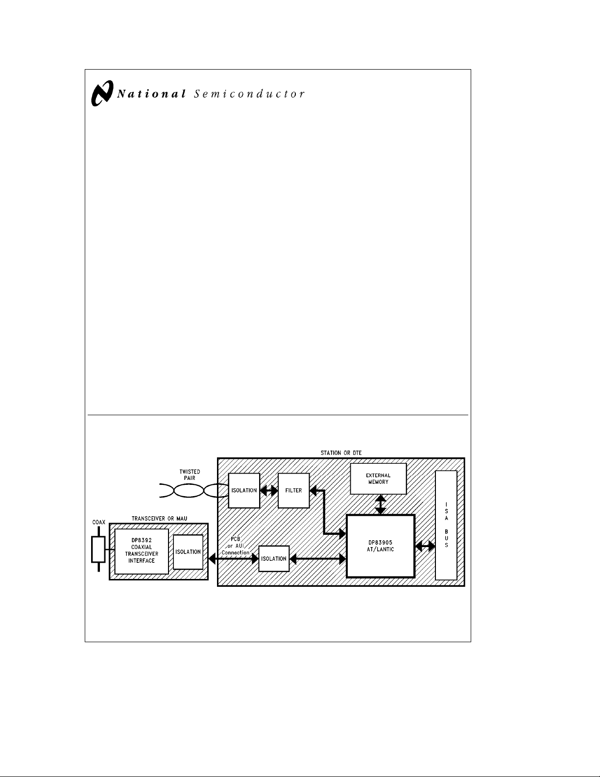
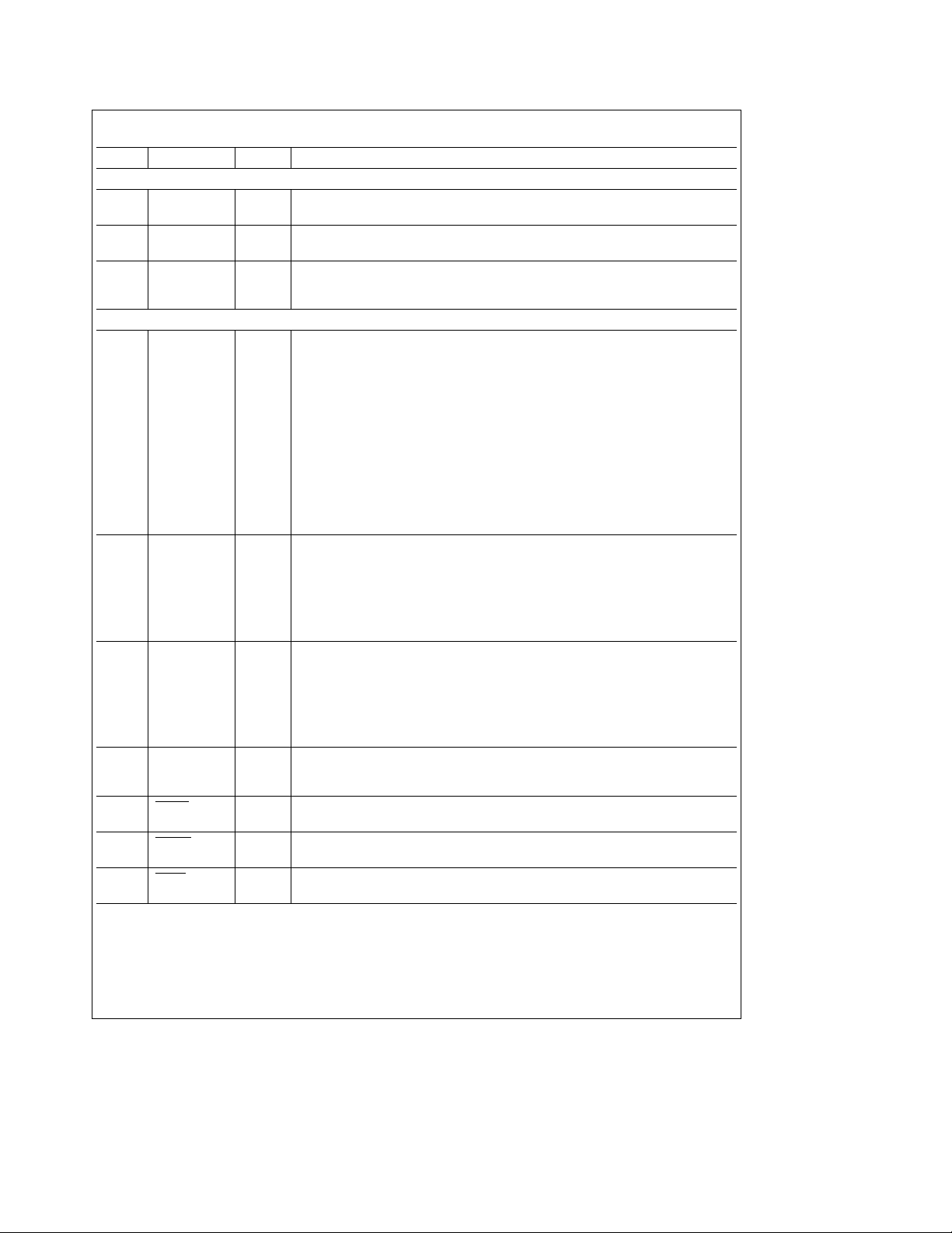
1.0 System Diagram
TL/F/11498– 1
TRI-STATEÉis a registered trademark of National Semiconductor Corporation.
TM
AT/LANTIC
PC-AT
Novell
EtherCard PLUS
C
1995 National Semiconductor Corporation RRD-B30M115/Printed in U. S. A.
is a trademark of National Semiconductor Corporation.
is a registered trademark of International Business Machines Corp.
É
is a registered trademark of Novell, Inc.
É
TM
and EtherCard PLUS 16TMare trademarks of Standard Microsystems Corp.
TL/F/11498
Page 2

General Description (Continued)
The integrated ENDEC module allows Manchester encoding and decoding via a differential transceiver and phase
lock Ioop decoder at 10 Mbit/sec. Also included are a collision detect translator and diagnostic loopback capability.
The ENDEC module interfaces directly to the transceiver
module, and also provides a fully IEEE compliant AUI (Attachment Unit Interface) for connection to other media
transceivers.
Table of Contents
1.0 SYSTEM DIAGRAM
1.1 Connection Diagram
2.0 PIN DESCRIPTION
3.0 SIMPLIFIED APPLICATION DIAGRAM
4.0 FUNCTIONAL DESCRIPTION
4.1 Bus Interface Block
4.2 Power on RESET operation
4.3 EEPROM Operation
4.4 Jumpered and Jumperless Operation Support
4.5 Low Power Operation
4.6 Boot PROM Operation
4.7 DP8390 Core (Network Interface Controller)
4.8 Twisted Pair Interface Module
4.9 Encoder/Decoder (ENDEC) Module
The Media Access Control function which is provided by the
Network Interface Control module (NIC) provides simple
and efficient packet transmission and reception control by
means of off-board memory which can be accessed either
through an I/O port or mapped into the system memory.
AT/LANTIC Controller provides a comprehensive solution
for 10BASE-T IEEE 802.3 networks. Due to the inherent
constraints of CMOS processing, isolation is required at the
AUI differential signal interface for 10BASE5 and 10BASE2
applications.
5.0 REGISTER DESCRIPTIONS
5.1 Configuration Registers
5.2 Shared Memory Mode Control Registers
5.3 NIC Core Registers
5.4 DP8390 Core DMA Registers
6.0 OPERATION OF AT/LANTIC CONTROLLER
6.1 Transmit/Receive Packet Encapsulation/
Decapsulation
6.2 Buffer Memory Access Control (DMA)
6.3 Packet Reception
6.4 Packet Transmission
6.5 Loopback Diagnostics
6.6 Memory Arbitration and Bus Operation
6.7 Functional Bus Timing
7.0 PRELIMINARY ELECTRICAL CHARACTERISTICS
8.0 PRELIMINARY SWITCHING CHARACTERISTICS
9.0 AC TIMING TEST CONDITIONS
2
Page 3
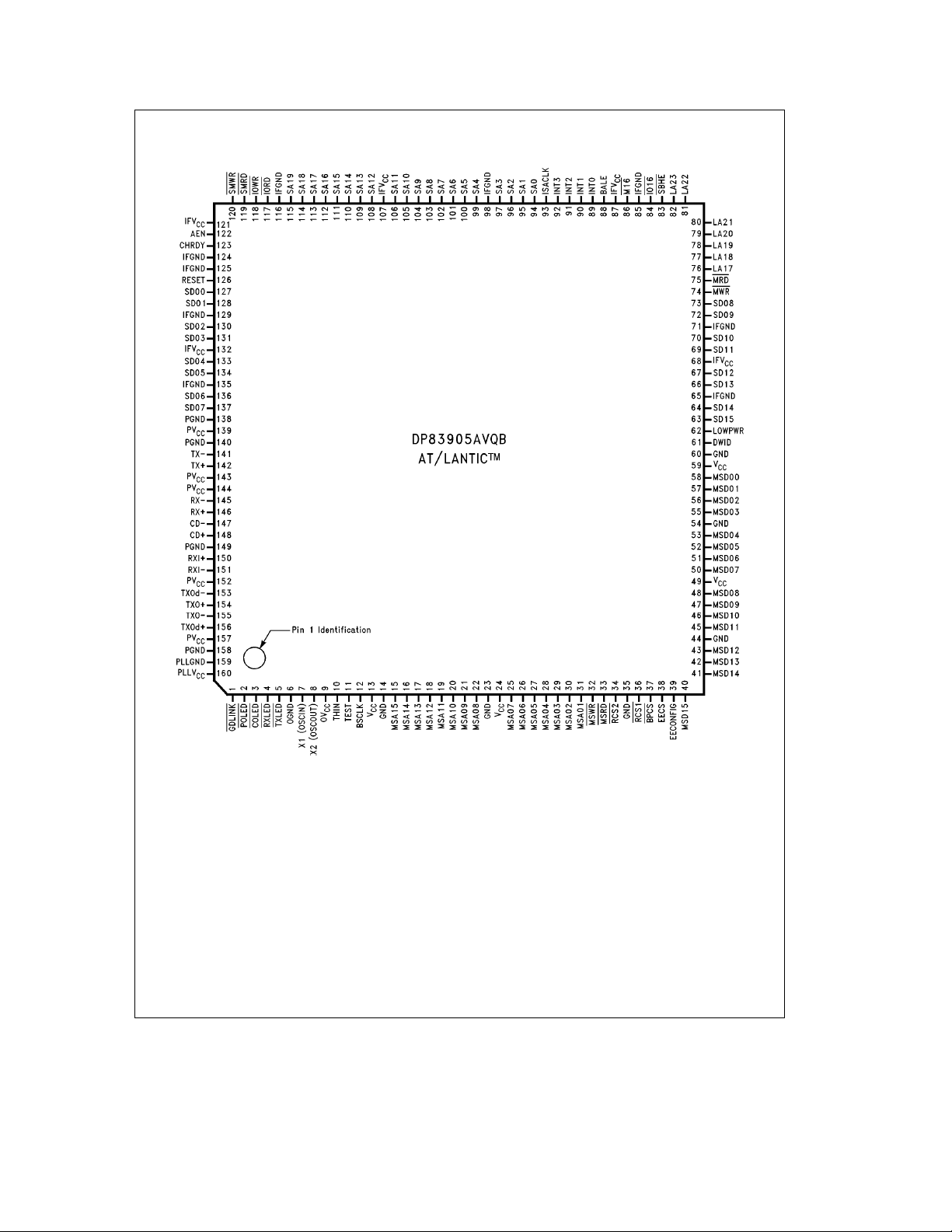
1.0 System Diagram (Continued)
1.1 CONNECTION DIAGRAM
Order Number DP83905AVQB
See NS Package Number VUL160A
3
TL/F/11498– 2
Page 4
2.0 Pin Description
Pin No. Pin Name Type* Description
ISA BUS INTERFACE PINS
94–97 SA0–SA1 9 I LATCHED ADDRESS BUS: Low-order 20 bits of the system’s 24 bit address bus.
99–106 TTL
108–115
76–82 LA17–LA23 I UNLATCHED ADDRESS BUS: High order 7 bits of the 24-bit system address bus.
127, 128, SD0–SD15 I/O SYSTEM DATA BUS: 16-bit system data bus. Used to transfer data between the
130, 131, 3SH
133, 134,
136, 137,
73, 72,
70, 69,
67, 66,
64, 63
88 BALE I BUS ADDRESS LATCH ENABLE: This signal indicates when the system address
83 SBHE I SYSTEM BUS HIGH ENABLE: This signal indicates that the system expects a
86 M16 O 16-BIT MEMORY TRANSFER: In 16-bit shared memory mode this signal indicates
84 IO16 O 16-BIT I/O TRANSFER: In I/O mode this signal indicates that the AT/LANTIC
74 MWR I MEMORY WRITE STROBE: Strobe from system to write to AT/LANTIC Controller’s
75 MRD I MEMORY READ STROBE: Strobe from system to read from AT/LANTIC Controller’s
119, SMRD &ILOW MEMORY STROBES: In Memory mode these signals strobe memory transfers
120 SMWR
118 IOWR I I/O WRITE STROBE: Strobe from system to write to the AT/LANTIC Controller’s I/O
117 IORD I I/O READ STROBE: Strobe from system to read from the AT/LANTIC Controller’s
126 RESET I RESET: This signal is output by the system to reset all devices on the bus.
*Driver Types are: IeInput, OeOutput, I/OeBi-directional Output, OCHeOpen Collector, 3SHeTRI-STATE Output, TTLeTTL Compatible, AUI
Attachment Unit Interface, TPIeTwisted Pair Interface, LEDeLED Drive, MOSeCMOS Level Compatible, XTALeCrystal.
These lines are enabled onto the bus, by the system, when BALE is high and are
Iatched when BALE returns Iow. These bits are used to decode accesses to the
AT/LANTIC Controller’s I/O map and to the boot PROM. In addition they are used to
decode accesses to the AT/LANTIC Controller’s memory in shared memory mode.
These Iines are valid on the falling edge of BALE. These bits are used to decode
TTL
accesses to the AT/LANTIC Controller’s memory in shared memory mode.
system and the AT/LANTIC Controller.
lines are valid.
TTL
transfer on the upper byte lane.
TTL
that the AT/LANTIC Controller has decoded an address within the 128 kbyte space
OCH
that it occupies part of.
Controller is responding to a 16-bit I/O access by driving 16-bits of data on the bus.
OCH
memory map.
TTL
to operate correctly
memory map.
TTL
to operate correctly
in the same manner as MRD
TTL
This pin should be connected to allow the CHRDY fix in 16-bit I/O mode
. (See Section 6.0)
This pin should be connected to allow the CHRDY fix in 16-bit I/O mode
. (See Section 6.0)
and MWR except that these signals only occur if the
access is to the lowest 1 Megabyte. This partial address decode means that these
signals can be used in an 8-bit slot to properly decode an access to this area.
AT/LANTIC Controller will use MRD
and SMWR in Memory mode when DWID is low (8-bit mode).
SMRD
SMWR
are also used to access the BOOT PROM.
map.
TTL
I/O map.
TTL
and MWR in 16-bit Memory mode and will use
TTL
The
SMRD and
e
4
Page 5
2.0 Pin Description (Continued)
Pin No. Pin Name Type* Description
ISA BUS INTERFACE PINS (Continued)
123 CHRDY O CHANNEL READY: This signal is used to insert wait states into system accesses.
122 AEN I DMA ACTIVE: This signal indicates that the system’s DMA controller has control
89–92 INT0–3 O INTERRUPT REQUEST: The operation of these 4 outputs is determined by the
61 DWID I DATA WIDTH: This input specifies whether the AT/LANTIC Controller is
93 lSACLK I ISA CLOCK: Clock from ISA bus. This signal is only required if CHRDY timing has
NETWORK INTERFACE PINS
156–153 TXOda, TXOb,OTWISTED PAIR TRANSMIT OUTPUTS: These high drive CMOS level outputs
a
, TXOd
TXO
150, 151 RXIa, RXI
141, TX
142 TX
145, RX
146 RX
147, CD
148 CD
b
b
a
b
a
b
a
5 TXLED O TRANSMIT: An open-drain active Iow output. It is asserted for approximately
4 RXLED O RECEIVE: An open-drain active low output. It is asserted for approximately 50 ms
3 COLED O COLLISION: An open-drain active Iow output. It is asserted for approximately 50
1 GDLNK O GOOD LINK: An open-drain active low output. This pin operates as an output to
2 POLED O POLARITY: An open-drain active low output. This signal is normally inactive.
*Driver Types are: IeInput, OeOutput, I/OeBi-directional Output, OCHeOpen Collector, 3SHeTRI-STATE Output, TTLeTTL Compatible, AUI
Attachment Unit Interface, TPIeTwisted Pair Interface, LEDeLED Drive, MOSeCMOS Level Compatible, XTALeCrystal.
OCH
of the bus.
TTL
Configuration registers. They can either be used to directly drive the interrupt lines
3SH
or used as a 3-bit code with a strobe to generate up to 8 interrupts.
interfacing to an 8- or 16-bit ISA bus. When high it is in 16-bit mode. It has an
MOS
internal pull-down resistor.
to be altered, by changing the CHRDY bit of Configuration Register B.
TTL
b
are resistively combined external to the chip to produce a differential output signal
TPI
with equalization to compensate for Intersymbol Interference (lSI) on the twisted
pair medium.
I TWISTED PAIR RECEIVE INPUTS: These inputs feed a differential amplifier
which passes valid data to the ENDEC module.
TPI
O AUI TRANSMIT OUTPUT: Differential driver which sends the encoded data to the
transceiver. The outputs are source followers which require 270X pull-down
AUI
resistors.
I AUI RECEIVE INPUT: Differential receive input pair from the transceiver.
AUI
I AUI COLLISION INPUT: Differential collision pair input from the transceiver.
AUI
50 ms whenever the AT/LANTIC Controller transmits data in either AUI or TPI
LED
modes.
whenever receive data is detected in either AUI or TPI mode.
LED
ms whenever the AT/LANTIC Controller detects a collision in either AUI or TPI
LED
modes.
display link integrity status if this function has not been disabled by the GDLNK bit
LED
in Configuration Register B.
This output is off if the AT/LANTIC Controller is in AUI mode or if link testing is
enabled and the link integrity is bad (i.e. the twisted pair link has been broken).
This output is on if the AT/LANTIC Controller is in Twisted Pair Interface (TPI)
mode, link integrity checking is enabled and the link integrity is good (i.e. the
twisted pair link has not been broken) or if the link testing is disabled.
When the TPI module detects seven consecutive link pulses or three consecutive
LED
received packets with reversed polarity POLED
is asserted.
e
5
Page 6
2.0 Pin Description (Continued)
Pin No. Pin Name Type* Description
NETWORK INTERFACE PINS (Continued)
7 X1 (OSCIN) I CRYSTAL OR EXTERNAL OSCILLATOR INPUT
8 X2 (OSCOUT) O CRYSTAL FEEDBACK OUTPUT: Used in crystal connections only. Should be left
10 THIN O THIN CABLE: This output is high if AT/LANTIC Controller is configured for thin
EXTERNAL MEMORY SUPPORT
58–50 MSD0–7, I/O, I, O MEMORY SUPPORT DATA BUSÐCONFIGURATION REGISTER A INPUT
CA0–7, MOS
DO, DI, SK
48–45 MSD8–15 or I/O, I MEMORY SUPPORT DATA BUSÐCONFIGURATION REGISTER B INPUT:
43-40 CB0– 7 MOS MSD8– 15: When RESET is inactive these pins can be used to access external
31–25, MSA1 –8 or O, I MEMORY SUPPORT ADDRESS BUSÐCONFIGURATION REGISTER C INPUT:
22 CC0 –7 MOS MSA1– 8: When RESET is inactive these pins drive the memory support address
21–15 MSA9–15 O MEMORY SUPPORT ADDRESS BUS: MSA9– 15: When RESET is inactive these
33 MSRD O MEMORY SUPPORT BUS READ: Strobes data from the external RAM into the AT/
32 MSWR O MEMORY SUPPORT BUS WRITE: Strobes data from the AT/LANTIC Controller
37 BPCS O BOOT PROM CHIP SELECT: Selects the boot PROM on the memory support data
*Driver Types are: IeInput, OeOutput, I/OeBi-directional Output, OCHeOpen Collector, 3SHeTRI-STATE Output, TTLeTTL Compatible, AUI
Attachment Unit Interface, TPIeTwisted Pair Interface, LEDeLED Drive, MOSeCMOS Level Compatible, XTALeCrystal.
XTAL
XTAL
DCDC
MOS
MOS
MOS
MOS
completely unconnected when using an oscillator module.
cable. It can be used to enable the DC-DC converter required by the thin ethernet
configuration.
EEPROM SIGNALS:
MSD0–7: When RESET is inactive these pins can be used to access external
memory and boot PROM.
CA0–7: When RESET is active Configuration Register A is loaded with the data
value on these pins. If the user puts an external pull-up on any of these pins then the
corresponding register bit is set to a 1. If the pin is left unconnected then the register
bit is 0.
DO, DI, SK: When RESET goes from an active to an inactive level AT/LANTIC
Controller will read the contents of an EEPROM, using these signals, and load the
contents into internal registers. These internal registers will then be mapped into the
space taken up by the PROM in the NE2000 and Ethercard PLUS16. After the
EEPROM read operation has completed these pins will revert to MSD0 –2 (D0
e
MSD0, DIeMSD1, SKeMSD2).
memory.
CB0–7: When RESET is active Configuration Register B is loaded with the data
value on these pins. If the user puts an external pull-up on any of these pins then the
corresponding register bit is set to a 1. If the pin is left unconnected then the register
bit is 0.
bus.
CC0–7: When RESET is active Configuration Register C is loaded with the data
value on these pins. If the user puts an external pull-up on any of these pins then the
corresponding register bit is set to a 1. If the pin is left unconnected then the register
bit is 0.
pins drive the memory support address bus. When the memory is only 8 bits wide A0
will appear on A13, in compatible mode, and on A15, in non-compatible mode.
LANTIC Controller via the memory support data bus.
into the external RAM via the memory support data bus.
bus.
e
6
Page 7

2.0 Pin Description (Continued)
Pin No. Pin Name Type* Description
EXTERNAL MEMORY SUPPORT (Continued)
36 RCS1 O RAM CHIP SELECT 1: Drives the chip select of the external RAM on the lower half
34 RCS2 O RAM CHIP SELECT 2: Drives the chip select of the external RAM on the upper half
38 EECS O EEPROM CHIP SELECT: Strobes data from the EEPROM onto the memory support
39 EECONFIG I CONFIGURE FROM EEPROM: When this pin is tied high the AT/LANTIC Controller
12 BSCLK I INTERNAL BUS CLOCK: This controls the speed of the NIC core if it is not running
LOW POWER SUPPORT
62 LOWPWR I LOW POWER: Instructs AT/LANTIC Controller to enter its low power mode, as
TEST SUPPORT
11 TEST I TEST: This input is only used for test mode. It should be left unconnected as it has
POWER SUPPLY PINS
160 PLLV
CC
159 PLLGND PLL NEGATIVE (GROUND) SUPPLY PINS
157, 152, PV
144, 143,
CC
139
158, 149, PGND PHYSICAL LAYER NEGATIVE (GROUND) SUPPLY PINS: These pins are the
140, 138
9OV
CC
6 OGND OSCILLATOR NEGATIVE (GROUND) SUPPLY PINS: This pin is the ground to the
59, 49, V
24, 13
CC
60, 54, 44, GND NEGATIVE (GROUND) SUPPLY PINS: These are the supply pins for the
35, 23, 14
132, 121, IFV
107, 87, 68
CC
135, 129, lFGND INTERFACE NEGATIVE (GROUND) SUPPLY PINS: These are the supply pins for
125, 124,
116, 98,
85, 71, 65
*Driver Types are: IeInput, OeOutput, I/OeBi-directional Output, OCHeOpen Collector, 3SHeTRI-STATE Output, TTLeTTL Compatible, AUI
Attachment Unit Interface, TPIeTwisted Pair Interface, LEDeLED Drive, MOSeCMOS Level Compatible, XTALeCrystal.
of the memory support data bus.
MOS
of the memory support data bus.
MOS
data bus.
MOS
loads the configuration from an EEPROM.
TTL
off of an internal clock (see Configuration Register C). This pin should be tied to
TTL
ground if it is unused.
detailed in Section 4.5. Should be tied to ground for normal operation.
TTL
an internal pull-down resistor which will enable correct operation.
MOS
PLL 5V SUPPLY PINS: This pin supplies 5V to the AT/LANTIC’s analog PLL inside
the ENDEC block. To maximize data recovery it is recommended that analog layout
and decoupling rules be applied between this pin and PLLGND.
PHYSICAL MEDIA 5V SUPPLY PINS: These pins supply 5V to the AT/LANTIC’s
analog physical media interface circuitry.
ground to the AT/LANTIC’s analog physical media interface circuitry.
OSClLLATOR 5V SUPPLY PINS: This pin supplies 5V to the AT/LANTIC’s oscillator
and LED circuitry.
AT/LANTIC’s oscillator and LED circuitry.
POSITIVE 5V SUPPLY PINS: These pins supply power to the AT/LANTIC
Controller’s logic.
AT/LANTIC Controller’s logic. It is suggested that decoupling capacitors be
connected between the V
for the GND pins with the lowest possible impedance.
and GND pins. It is essential to provide a path to ground
CC
INTERFACE POSITIVE 5V SUPPLY PINS: These pins supply power to the
AT/LANTIC Controller’s ISA interface.
the AT/LANTIC Controller’s ISA interface. It is suggested that decoupling capacitors
be connected between the IFV
ground for the IFGND pins with the lowest possible impedance.
and IFGND pins. It is essential to provide a path to
CC
e
7
Page 8
3.0 Simplified Application Diagram
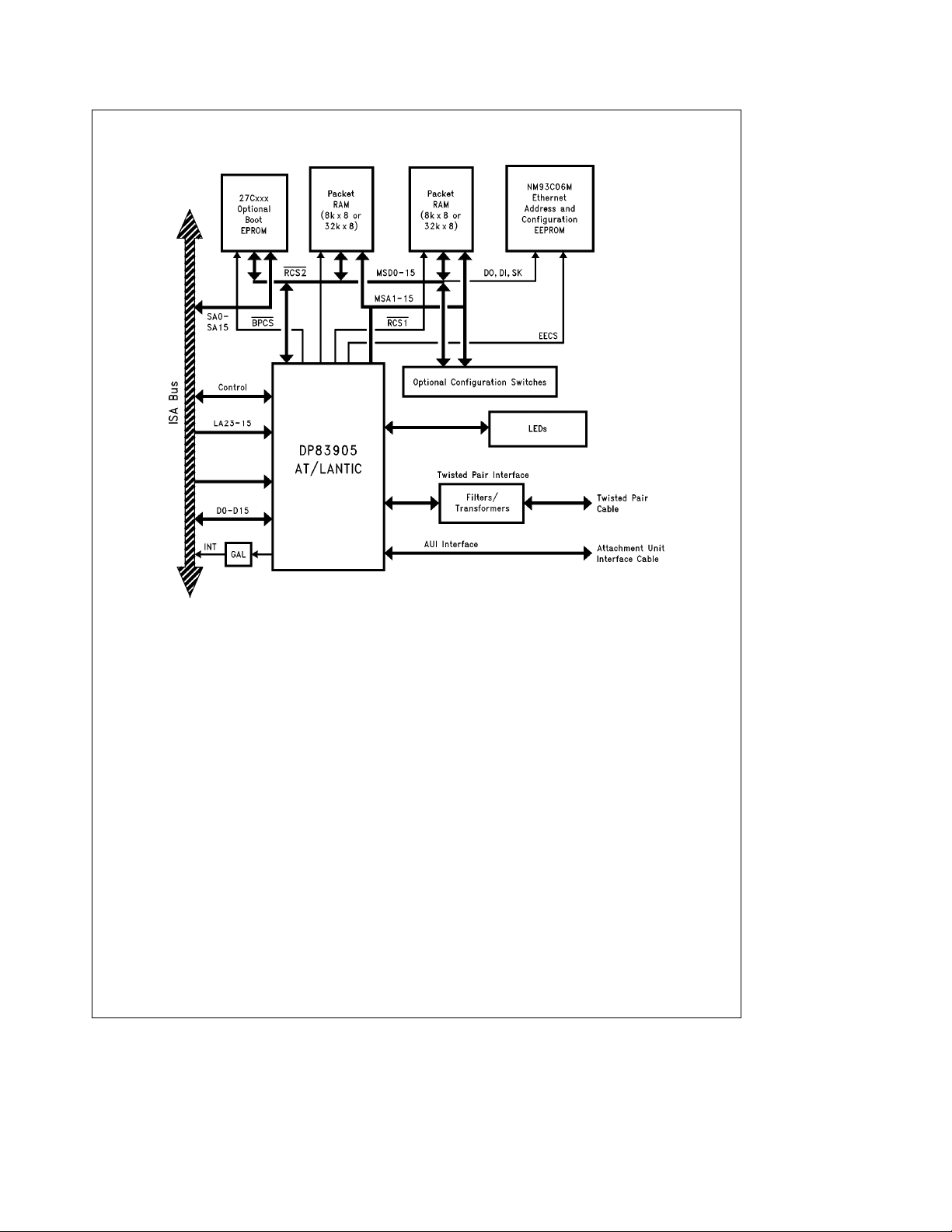
4.0 Functional Description
The AT/LANTIC Controller is a highly integrated and configurable Ethernet controller making it suitable for most Ethernet applications. The AT/LANTIC Controller integrates the
functions of the following blocks:
1. DP8390 Ethernet Controller Core and Media Access
Control logic.
2. ISA Bus Interface containing all logic required to connect
the DP8390 core to a packet buffer RAM and the ISA
bus.
3. Media Interface which includes an Encoder/Decoder
block with an AUI (Attachment Unit Interface) and a
10BASE-T Twisted Pair Interface.
TL/F/11498– 3
4.1 BUS INTERFACE BLOCK
The AT/LANTIC Controller’s Bus interface block provides
the circuitry to interface the Ethernet controller logic, and
the external packet buffer RAM to an ISA (Industry Standard
Architecture) Bus. The bus interface provides several configuration modes which offer various different features depending on the designer’s specific design requirements.
The possible modes are:
1. 16-Bit or 8-Bit Shared Memory Compatible Mode
2. 16-Bit or 8-Bit Shared Memory Enhanced Mode
3. 16-Bit or 8-Bit I/O Port Compatible Mode
4. 16-Bit or 8-Bit I/O Port Enhanced Mode
This section describes the function of each of these modes.
8
Page 9
4.0 Functional Description (Continued)
FIGURE 1. Block Diagram of AT/LANTIC Controller
DETERMINING 8- OR 16-BIT WIDE DATA
AT/LANTIC Controller can treat the system data bus and all
internal data busses as 8 or 16 bits wide. 8- or 16-bit mode
is determined by the DWlD pin. For an adapter card this bit
can be used to automatically detect if the card has been
plugged into an 8- or 16-bit slot. If this pin is connected to a
V
on the upper connector it will be high when plugged
DD
into a 16-bit slot, enabling 16-bit mode, and floating when
plugged into an 8-bit slot. When floating the internal pulldown resistor will enable 8-bit mode.
SHARED MEMORY ARCHITECTURE
FIGURE 2. Shared Memory
TL/F/11498– 5
TL/F/11498– 4
In this mode the AT/LANTIC Controller’s internal memory
map, using external RAM devices, is mapped into the host
system’s memory map. Both the AT/LANTIC Controller and
the host system can directly access this memory. The
AT/LANTIC Controller controls the arbitration for this memory area, giving priority to its internal accesses. It also has
an internal FIFO to allow for any latency on internal transfers introduced by system accesses. If a system access occurs while an internal access is current the AT/LANTIC
Controller will insert wait states into the system cycle until
the internal transfer is complete.
In this mode the AT/LANTIC Controller’s internal registers
are accessed within the system’s I/O map. The address
within this I/O map is set by Configuration Register A. The
user programs the address of the shared memory within the
host systems memory map by writing to a register in
AT/LANTIC Controller. The memory is not accessible by
the user until after this register has been programmed.
There are two basic Shared Memory modes, compatible
mode, and non-compatible mode, as described in the following text.
9
Page 10
4.0 Functional Description (Continued)
Shared Memory Compatible Mode I/O Address
Mapping
The shared memory is at an address decided by the Address Decode Register and the base I/O address of
AT/LANTIC Controller is configured in Configuration Register A. At that address the following structure appears.
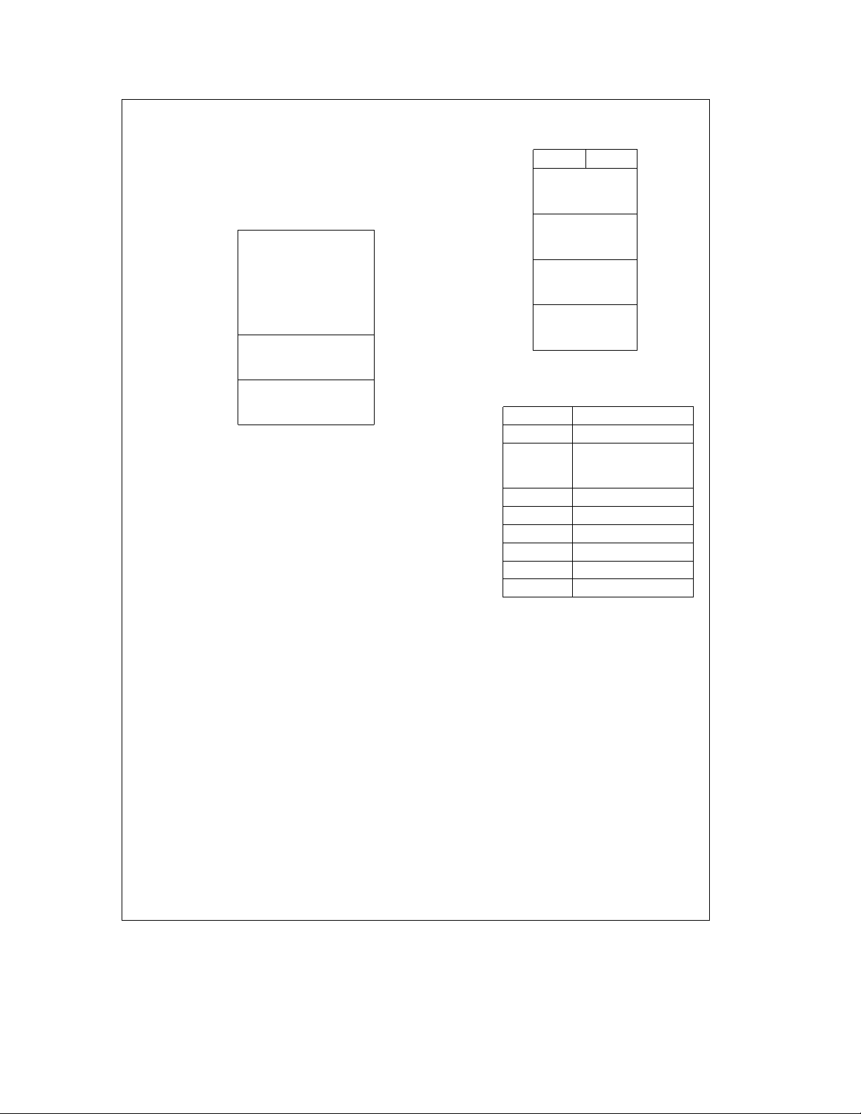
Addr D7– 0
00 Control 1
01 AT detect (Read only)
02 Unused
03 Unused
04 Unused
05 Control 2
06 Unused
07 Unused
08 Node addr 0 (Read only)
09 Node addr 1 (Read only)
0A Node addr 2 (Read only)
0B Node addr 3 (Read only)
0C Node addr 4 (Read only)
0D Node addr 5 (Read only)
0E 05h (Read only)
0F Checksum (Read only)
10
to
1F
0000H
NIC
registers
(a)
D15 D0
8kx16
Buffer RAM
specified as the PROM space for compatibility with the Ethercard PLUS16. This is actually an array of 8-bit registers
which are loaded from an external EEPROM after
AT/LANTIC Controller is initialized by a reset pulse. The
user should program the EEPROM to contain these values.
The 8k words of memory can be accessed directly by the
host system in the same manner as any other memory. Typically the programmer would remove data from this buffer
using a ‘‘MOV’’ or ‘‘MOVSW’’ instruction.
8-BIT SHARED MEMORY COMPATIBLE MODE
In this mode the I/O map remains the same. The NIC core
can still operate in 16-bit mode, if bit 6 of Control Register 2
is set high and the full 16 kbytes of RAM are still available.
However, only 8-bit system accesses are allowed. If bit 6 of
Control register 2 is low the NIC core must operate in 8-bit
mode and only 8k of memory is available. The NIC Core
data width is set by the WTS bit in the Data Configuration
Register.
A low cost card, using only one 8 kbyte RAM, can be designed. If the DWlD pin is left unconnected, or tied to GND,
then the AT/LANTIC Controller will always operate in 8-bit
mode, regardless of the slot the board is in.
If DWID is low the address bits of Control Register 2 should
not be written to as they have no effect. In this mode the
address comparator assumes that SA19 is to be compared
to a logic high, with the other address comparisons programmed into Control Register 1.
SHARED MEMORY NON-COMPATIBLE MODE
These modes are similar to the compatible mode. The difference is that they map a full 64 kbytes of RAM into the
PC’s memory address space. The I/O map remains the
same.
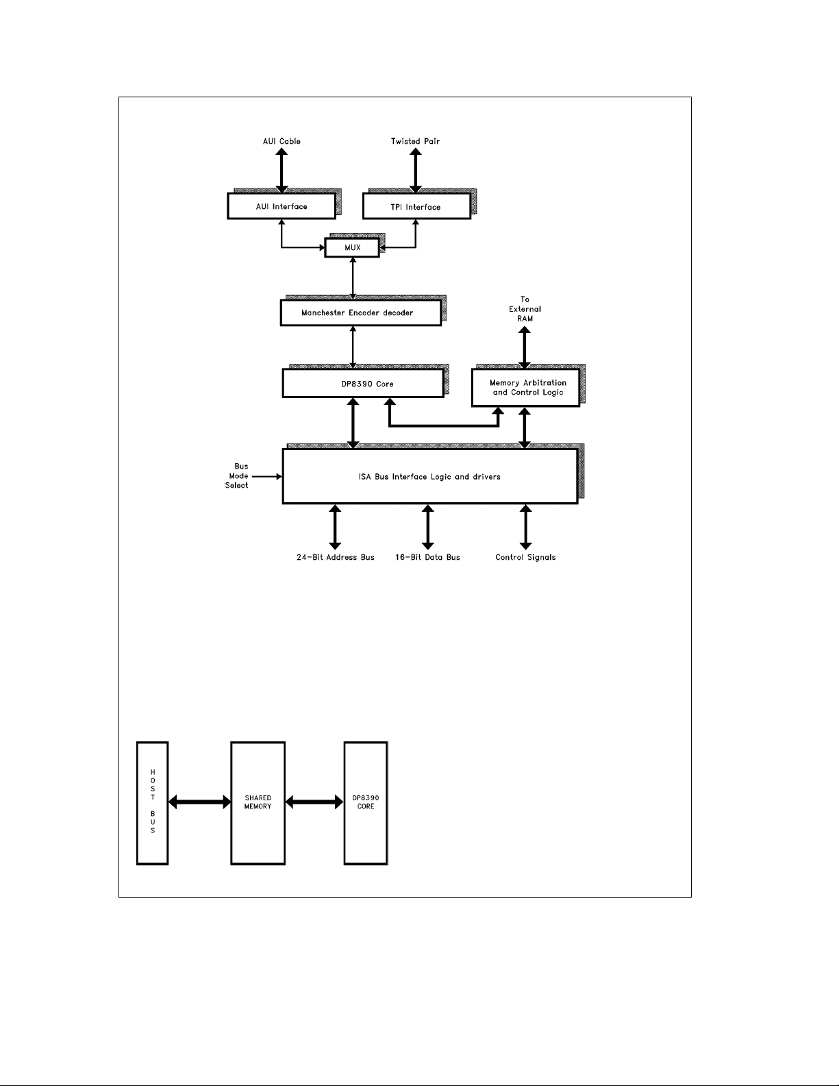
I/O PORT ARCHITECTURE
4000H
8000H
C000H
FFFFH
FIGURE 3. Shared Memory Mode a) Register
Mapping and b) NIC Core Memory Map
The AT Detect Register indicates whether AT/LANTIC Controller is in an 8- or 16-bit slot. The least significant bit of this
register is set high when AT/LANTIC Controller is in 16-bit
mode and low in 8-bit mode. Addresses 08H to 10H are
Aliased
Buffer RAM
Aliased
Buffer RAM
Aliased
Buffer RAM
(b)
FIGURE 4. I/O Port
TL/F/11498– 6
This is the architecture used by Novell’s NE2000. In this
mode the AT/LANTIC Controller’s internal memory map is
accessed byte or word at a time, via a port within the system’s I/O space. AT/LANTIC Controller is programmed by
the user to control the transfers between its internal memory and the I/O port.
In this mode the AT/LANTIC Controller’s internal registers
and the memory access port are accessed within the system’s I/O map. The address within this I/O map is set by
Configuration Register A.
10
Page 11
4.0 Functional Description (Continued)
16-BIT I/O PORT COMPATIBLE MODE I/O ADDRESS
MAPPING
This mode is compatible with Novell’s NE2000. The base
I/O address of the AT/LANTIC Controller is configured by
Configuration Register A (either upon power up or by software writing to this register). At that address the following
structure appears.
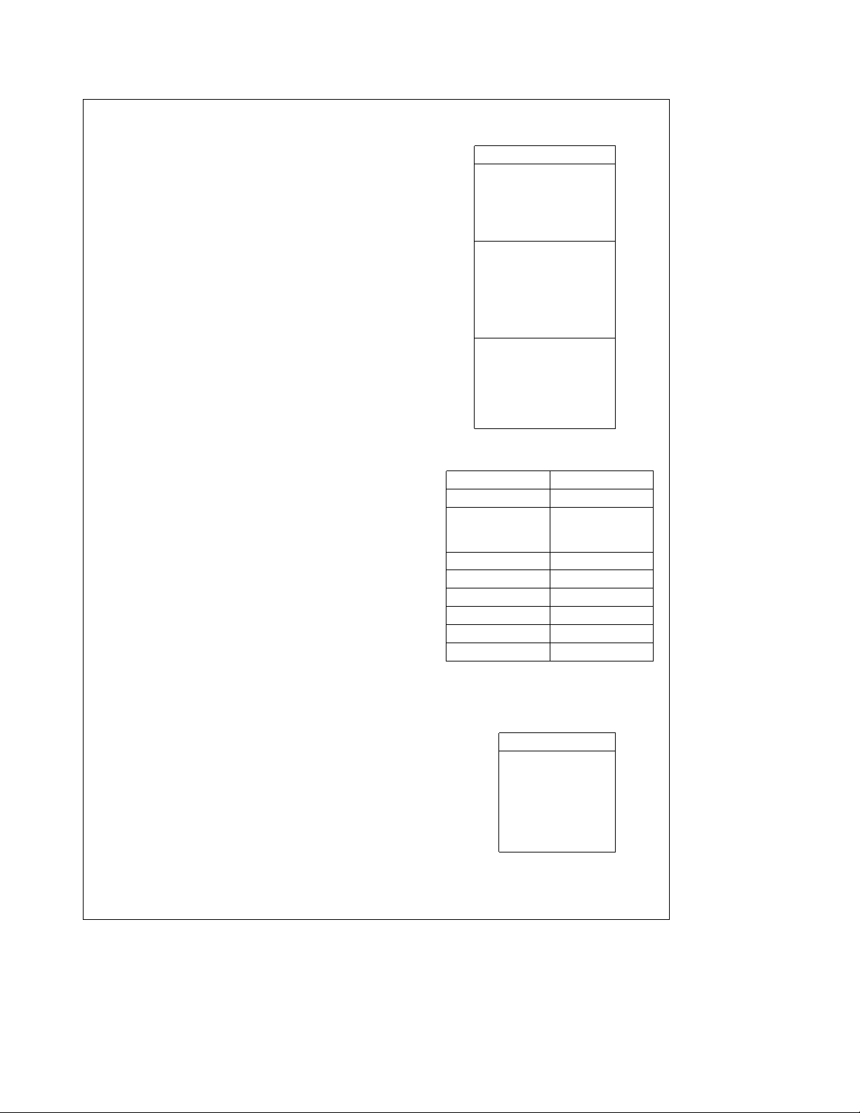
Basea00H
DP8390
Core
Registers
Basea0FH
Basea10H
a
Base
17H
Basea18H
a
Base
1FH
FIGURE 5. I/O Port Mode Register I/O Map
The registers within this area are 8 bits wide, but the data
transfer port is 16 bits wide. The AT/LANTIC Controller’s
registers can be programmed to control the passing of data
between its internal memory and the data transfer port. By
accessing the data transfer port (using I/O instructions) the
user can transfer data to or from the AT/LANTIC Controller’s internal memory. The AT/LANTIC Controller’s internal
memory map is as shown in
AT/LANTIC Controller actually has a 64k address range but
only does partial decoding on these devices. The PROM
data is mirrored at all decodes up to 4000H and the entire
map is repeated at 8000H. To access either the PROM or
the RAM the user must initiate a Remote DMA transfer between the I/O port and memory.
On a remote read the AT/LANTIC Controller moves data
from its internal memory map to the I/O port and the host
system reads it by using an ‘‘INW’’ or ‘‘INSW’’ instruction
from the I/O address of the data transfer port. If the system
attempts to read the port before AT/LANTIC Controller has
written the next word of data to it AT/LANTIC Controller will
insert wait states into the system cycle, using the CHRDY
Data Transfer Port
Reset Port
Figure 6
.
0000H
001FH
D15 D0
PROM
Aliased PROM
4000H
8kx16
7FFFH
Buffer RAM
8000H
Aliased PROM
C000H
Aliased
FFFFH
Buffer RAM
(a)
D15 D0
1EH 00 57H
1CH 00 57H
##
00 RESERVED
##
0AH 00 E’net Address 5
08H 00 E’net Address 4
06H 00 E’net Address 3
04H 00 E’net Address 2
02H 00 E’net Address 1
00H 00 E’net Address 0
(b)
FIGURE 6. a) NIC Core’s Memory Map
b) 16-Bit Prom Map
11
Page 12
4.0 Functional Description (Continued)
line. AT/LANTIC Controller will not begin the next memory
read until the previous word of data has been read.
On a remote write the system writes data to the I/O port,
using an ‘‘OUTW’’ or ‘‘OUTSW’’ instruction, and
AT/LANTIC Controller moves it to its buffer memory. If the
system attempts to write to the port before AT/LANTIC
Controller has moved the data to memory AT/LANTIC Controller will insert wait states into the system cycle, using the
CHRDY line. AT/LANTIC Controller will not begin the next
memory write until a new word has been written to the I/O
port.
Addresses 00H to 1FH are specified as the PROM space
for compatibility with the NE2000. This is actually an array of
8-bit registers which are loaded from an external EEPROM
after AT/LANTIC Controller is initialized by an ISA RESET.
They should contain the same data as the PROM did in the
NE2000 and in the same format. As can be seen the PROM
registers are only 8-bits wide. To transfer the data out the
user must initiate a 16-bit DMA read transfer and discard the
most significant byte of data on each transfer.
At address 00H of the PROM is a six byte Ethernet address
for this node. The upper two addresses of the PROM store
contain bytes which identify whether the AT/LANTIC Controller is in 8- or 16-bit mode. For 16-bit mode these bytes
both contain the value 57H, for 8-bit mode they both contain
42H.
8-BIT I/O PORT COMPATIBLE MODE
This mode is compatible with the 8-bit mode offered by
Novell’s NE2000. The NE2000 automatically detects whether it is in an 8- or 16-bit slot and configures itself appropriately. As explained in the previous paragraphs, the user can
determine whether the board is in 8- or 16-bit mode by reading the PROM. In 8-bit mode only 8 kbytes of RAM are
addressable, as in the 8-bit mode of the NE2000. The I/O
map is the same as the 16-bit mode, the memory map is
shown in
code, so is mirrored at all addresses up to 4000H. The
PROM still occupies 32 bytes of address space, although it
only has 16 bytes of data, as the data at all odd address
locations is merely a mirror of the data at the previous even
address location. The RAM is mirrored at 6000H and the
entire map mirrored at 8000H.
A low cost card, using only one 8 kbyte RAM, can be designed. If the DWlD pin is left unconnected, or tied to GND,
then the AT/LANTIC Controller will always operate in 8-bit
mode, regardless of the slot the board is in.
I/O PORT NON-COMPATIBLE MODE
This mode is similar to Novell’s NE2000, but this mode allows the user to use the full 64 kbytes of address space
except for an initial page for the PROM. The memory map
for this board is shown in
same for both 8- and 16-bit modes. Although the PROM
store occupies 256 bytes, it is only 16 bytes long. The entire
map is mirrored at 8000H.
A low cost card, using only one 8 kbyte RAM, can be designed. If the DWID pin is left unconnected, or tied to GND,
then the AT/LANTIC Controller will always operate in 8-bit
mode, regardless of the slot the board is in.
Figure 7
. Again the PROM has only a partial de-
Figure 8
. The memory map is the
0000h
0020h
4000h
6000h
8000h
1EH 42H 42H
1CH 42H 42H
PROM
Aliased PROM
8k x 8 BUFFER RAM
RESERVED
(a)
D15 D0
##
RESERVED RESERVED
##
0AH E’net Address 5 E’net Address 5
08H E’net Address 4 E’net Address 4
06H E’net Address 3 E’net Address 3
04H E’net Address 2 E’net Address 2
02H E’net Address 1 E’net Address 1
00H E’net Address 0 E’net Address 0
(b)
FIGURE 7. a) 8-Bit NIC Core’s Memory Map
0000H
00FFH
0100H
FFFFH
b) 8-Bit PROM Map
PROM
BUFFER RAM
FIGURE 8. I/O Port Enhanced Mode
DP8390 Core Memory Map
12
Page 13
4.0 Functional Description (Continued)
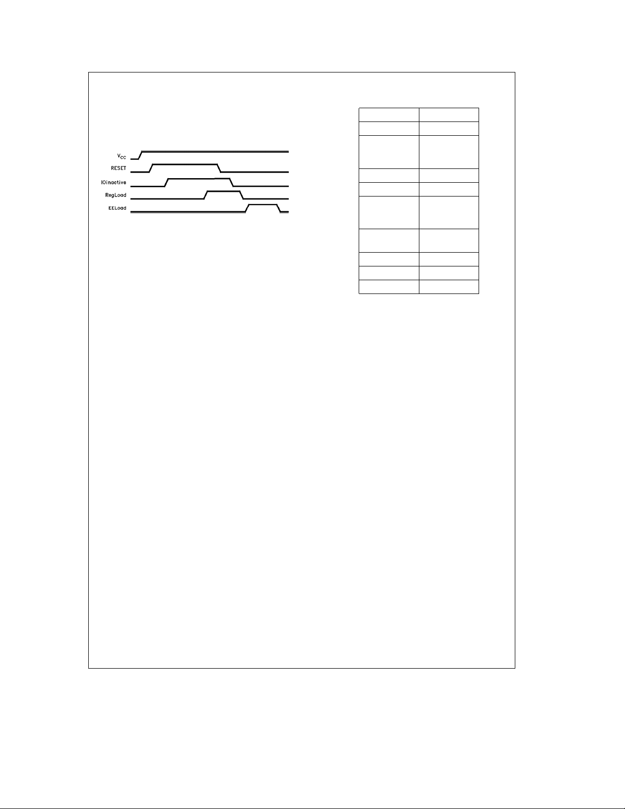
4.2 POWER ON RESET OPERATION
The AT/LANTIC Controller configures itself after a Reset
signal is applied. To be recognized as a valid Power-On-Reset the Reset signal must be active for at least 415 ms.
Figure 9
shows how the RESET circuitry operates.
FIGURE 9. RESET Operation
The ISA standard determines that within 500 ns of RESET
going active all devices should enter the appropriate reset
condition. The AT/LANTIC Controller will generate the internal signal IOinactive after RESET has been active for
415 ns, which will disable all outputs and cause RESET to
be the only input monitored. The AT/LANTIC Controller will
not respond to a RESET pulse of shorter duration than this.
An internal timer continues to monitor the amount of time
RESET is active. After 415 ms it is considered a valid PowerOn-Reset and an internal signal called RegLoad is generated.
When a Power-On-Reset occurs the AT/LANTIC Controller
latches in the values on the configuration pins and uses
these to configure the internal registers and options. Internally these pins contain pull-down resistors, which are enabled when IOinactive goes active. If any pins are unconnected they default to a logic zero. The internal pull-down
resistor has a high resistance to allow the external pull-up
resistors to be of a high value. This limits the current taken
by the memory support bus. The suggested external resistor
value is 10 kX. The configuration registers are loaded from
the memory support bus when RESET goes inactive if RegLoad is active. The internal pull-down resistors are enabled
onto the bus until RegLoad has gone inactive.
A Power-On-Reset also causes the AT/LANTIC Controller
to load the internal PROM store from the EEPROM, which
can take up to 320 ms. This occurs after RegLoad has gone
inactive. The AT/LANTIC Controller will be inaccessible during this time. If EECONFIG is held high the configuration
data loaded on the falling edge of RESET will be overwritten
with data read from the serial EEPROM. Regardless of the
level on EECONFIG the PROM store will always be loaded
with data from the serial EEPROM during the time specified
as EELoad.
4.3 EEPROM OPERATION
The AT/LANTIC Controller uses an NM93C06, or
EEPROM with compatible timings. The NM93C06 is a 256bit device, arranged as 16 words each 16 bits wide. The
programmed contents of the EEPROM is shown in
10
.
Mapping EEPROM Into PROM Space
Data is read from the EEPROM at boot time and stored in
registers within the AT/LANTIC Controller. While this operation takes place the AT/LANTIC Controller can not be ac-
TL/F/11498– 7
Figure
D15 D0
0FH 73H Config. C
0EH Config B Config. A
##
##
##
08H 42H 42H
07H 57H 57H
##
##
##
03H Reserved Reserved
(Checksum) (Board Type)
02H E’net Address 5 E’net Address 4
01H E’net Address 3 E’net Address 2
00H E’net Address 1 E’net Address 0
Note 1: The contents of locations 03H and 04H differ between I/O Mode
and Shared Memory Mode. The Shared Memory Mode values are shown in
parentheses. For compatibility with both modes default to the shared memory mode values.
Note 2: Programming 73H into the upper address is not absolutely required
but is strongly recommended for future compatibility of manufacturing process.
FIGURE 10. EEPROM Programming Map
cessed by the system. These registers are mapped into the
space traditionally occupied by the PROM in the NE2000 or
the EtherCard PLUS16. The size and format of this data
read is determined by the mode of operation.
SHARED MEMORY MODE
In this mode, program the EEPROM to contain the node’s
Ethernet address in the first six bytes, a byte identifying the
type of board AT/LANTIC Controller is emulating in byte 7
and a checksum byte in byte 8. The two’s complement sum
of these eight bytes should equal FFH.
In this Mode the AT/LANTIC Controller reads the first 4
words from the EEPROM and maps them into the I/O map
at the appropriate address.
I/O PORT MODE
In this mode, program the EEPROM to contain the node’s
Ethernet address in the first six bytes. The user should then
program 5757H and 4242H into the subsequent bytes. The
AT/LANTIC Controller will decide which of these values
should be loaded into the PROM store depending on the
DWlD pin. (The data width is programmed in this mode by
setting the WTS bit in the Data Configuration Register and
setting the DWlD pin for the proper mode.) If some other
numerical values are preferred to indicate the mode then
they can be programmed at this location in the EEPROM
and AT/LANTIC Controller will put them at the correct address.
In this mode the AT/LANTIC Controller reads the first 7
words from the EEPROM and maps them into the memory
map at the appropriate address. If in 16-bit mode it also
13
Page 14
4.0 Functional Description (Continued)
reads the next word in the EEPROM and appends this. If in
8-bit mode it skips a word, then reads and appends the next
word.
Storing and Loading Configuration from EEPROM
If the EECONFIG pin is high during boot up the AT/LANTIC
Controller’s configuration is read from the EEPROM, before
the PROM data is read. The configuration data is stored
within the upper two words of the EEPROM’s address
space. Configuration Registers A and B are located in the
lower of these words, Register C in the lower byte of the
upper word, as shown in
To write this configuration into the EEPROM the user must
follow the routine specified in the pseudo code below. This
operation will work regardless of the level on EECONFIG.
The EELOAD bit of Configuration Register B being set starts
the EEPROM write process. Care should be taken not to
accidently set the GDLINK bit and therefore disable link integrity checking. The next 3 writes to this register load the
values that will be stored in the configuration register (note
that the last 2 of these writes do not have to follow the
normal practice of preceding a write to this register with a
read to this address). The AT/LANTIC Controller will then
commence the EEPROM write. The write has been completed when the EELOAD bit goes to zero. This loading procedure should be followed exactly and interrupts should be
disabled until it has completed, to prevent any accidental
accesses to the AT/LANTIC Controller.
EEPROMÐLOAD()
À
DISABLEÐINTERRUPTS();
e
value
READ(CONFIGÐB);
e
value
value AND 1 GDLINK;
e
value
value OR EELOAD;
WRITE(CONFIGÐB, value);
READ(CONFIGÐB);
WRITE(CONFlGÐB, configÐforÐA);
WRITE(CONFIGÐB, configÐforÐB);
WRITE(CONFIGÐB, configÐforÐC);
while (value AND EELOAD)
À
valueeREAD(CONFIGÐB);
WAIT();
Ó
ENABLEÐINTERRUPTS();
Ó
4.4 JUMPERED AND JUMPERLESS OPERATION
SUPPORT
The AT/LANTIC Controller supports several options that
enable the implementation of either a ‘‘jumpered’’ or ‘‘jumperless’’ power on configuration when installed into a standard PC compatible’s ISA bus. A wide range of options are
provided to ensure that the AT/LANTIC Controller can be
configured by an end user to function in all possible PC-AT
system configurations. Several types of configuration options can be implemented examples including:
1. Full jumper options: All programmable options are selected by utilizing jumpers on the board. Option selection
requires no special software. An example of this is
shown in the
Figure 11
Figure 10
.
.
2. I/O address jumpers only: All other options configurable
via software. This option simplifies installation while maximizing compatibility.
3. Jumperless: Special scheme provides contention-free
I/O address selection.
The AT/LANTIC Controller’s Configuration Registers are
the key to providing the ability to implement various configuration options. These registers are configured by the same
method in shared memory and I/O port modes, 8- or 16-bit
modes. The bit definitions of these registers are provided in
Section 5. All three registers are configured by hardware
selection during the Power-On-Reset of the system. Two of
these registers can be configured via software (the Mode
Configuration Registers A and B). The third register (Hardware Configuration Register C) is only configured during reset.
The following table indicates
troller options that a designer may like to have user configurable. (This list does not represent the complete list. For the
full list see the Configuration register descriptions in
Section 5.)
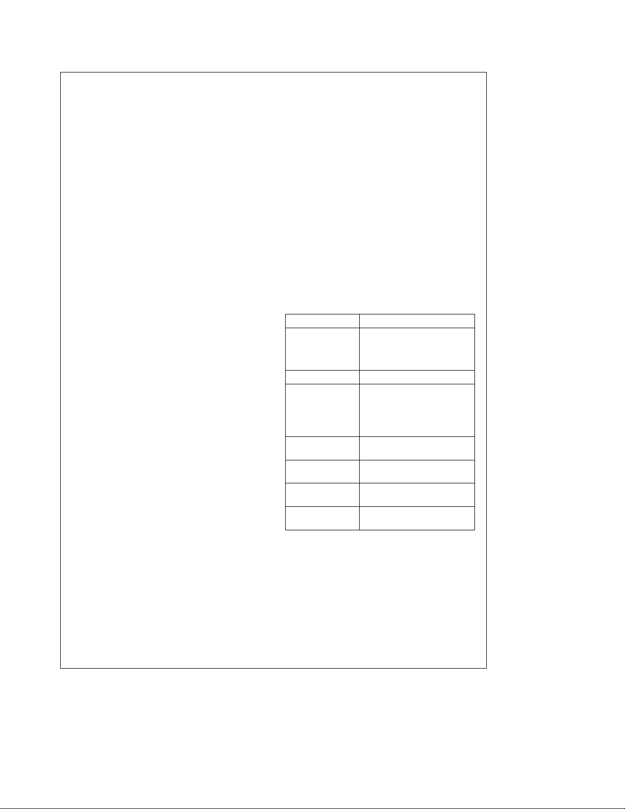
TABLE I. Some Configuration Options
for AT/LANTIC Controller
most
of the AT/LANTIC Con-
Option Selections
I/O Base Address 0300H 02C0H
Software 0320H
0240H 0340H
0280H 0360H
Interrupt No. 4 Interrupts 8 Interrupts
Boot PROM Disabled 0CC00H
Address 0C000H 0D000H
0C400H 0D400H
0C800H 0D800H
0DC00H
Boot PROM Size None 32k
16k 64k
Media Selection Twisted Pair Thin Ethernet
AUI Port
Architecture I/O Mode Shared RAM
Mode
Bus Timing IOCHRDY MEM16 Mode
Options Mode
The three basic options are described below. Because of
the variety of programmable options there are a number of
variations possible, only a few typical examples will be discussed.
FULLY JUMPERED OPERATION
This option is shown in
options are selected by jumpers on the AT/LANTIC Controller’s memory bus. For this option all configuration options
are set upon power-on by the AT/LANTIC Controller as described in Section 4.2. Accessing the configuration registers
is unnecessary and the EEPROM need only contain the
Figure 11
. In this configuration most
14
Page 15
4.0 Functional Description (Continued)
JP1. .JP3 I/O Address
JP4..JP5 INTR Jumper
JP6 IO OR Shared RAM
JP7, JP8 Thin, Thick or TP Interface
JP9, CHRDY Assertion
JP10..JP13 EPROM Address and Size
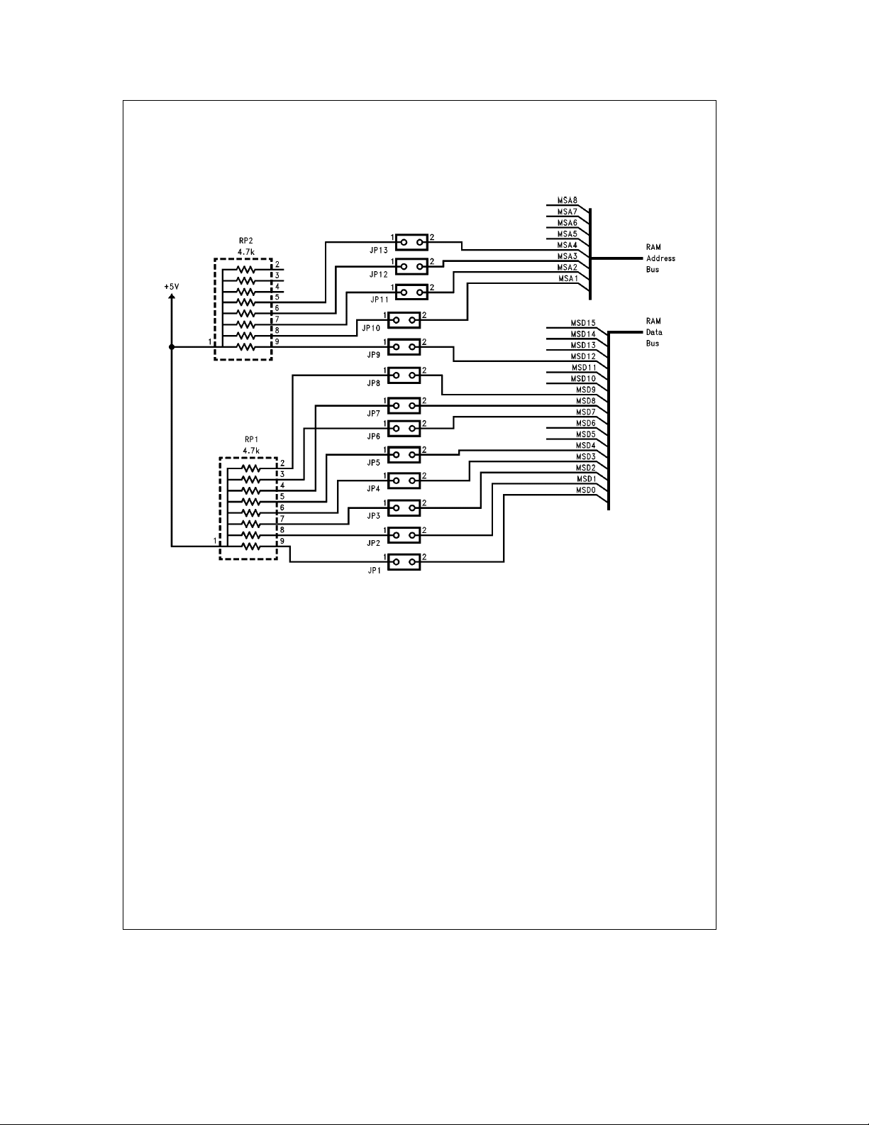
FIGURE 11. Example of Jumper Configuration
Ethernet ID address (Configuration Register B bit 7 should
be set to disable EEPROM configuration mode, and Configuration Register C bit 7 could be set to disable software
configuration completely).
MINIMAL JUMPERS
The AT/LANTIC Controller’s configuration registers provide
the capability to enable software to configure various options (some may be hardwired). For the one option that is
not easily configured on the ISA bus is the I/O address
options. The reason for this is that the I/O locations must
first be known by the software in order for the software (usually a device driver) to access the AT/LANTIC Controller.
However, upon power up, in order to access a register to
configure the I/O base address to avoid conflicts some default location must be given (typically set in hardware on the
memory bus). It is possible that this default location conflicts
with an already installed device. If this is the case then one
possible solution, is to provide a jumper option for only the
I/O Addresses. A similar situation exists for the boot PROM
memory addresses.
In this application all options except the I/O address and
the boot PROM are hardwired on the memory bus to a default setting. After power up software can change the con-
TL/F/11498– 8
figuration to avoid conflicts on these settings. The advantage of this approach is that for most systems the default
I/O address setting is the correct one and no installation will
be required in this case. This approach minimizes any compatibility issues.
NO JUMPERS
The conflicts possible in the I/O base selection can be overcome by a special mode for software configuration of the
I/O base address. By using this mode, and by using the
configuration storage capability of the EEPROM a fully software configurable design on the ISA bus can be realized
without address conflict problems.
This mode is invoked by having the AT/LANTIC Controller
default to jumperless software configuration option in the
I/O base selection. This mode enables configuration register A to be mapped to address location 278H which is defined to be a printer port’s data register. If software writes to
this location four consecutive times on the fourth write the
AT/LANTIC Controller will load the data written into the I/O
address bits of Configuration Register A. This data should
set the I/O base address to a known conflict-free value. The
AT/LANTIC Controller can now be configured and operated
15
Page 16

4.0 Functional Description (Continued)
at the desired base I/O address. If desired the configuration
software could change the EEPROM content to the new
values eliminating the need to reconfigure upon each power
up. Alternately the software could leave the EEPROM alone
and execute the configuration using the printer port’s data
register upon each power up. This configuration scheme will
only work once after each power-up. Therefore the user
cannot enable the AT/LANTIC Controller from reserved
mode, change it back into reserved mode, and enable it
again. A power-on reset must occur between the first time it
is enabled from the reserved mode and the second.
A second consideration is the location of the boot PROM in
the system memory map, which also has the same conflict
and programming considerations as the I/O address selection. However the solution is different, primarily because the
boot PROM must be configured before power up. This is
because during normal usage of the boot PROM the PC’s
BIOS will look for the ROM immediately after reset, not allowing configuration software to first select the boot PROM
addressing prior to usage.
To configure the boot PROM without jumpers the configuration software must first power up the AT/LANTIC Controller,
configure the EEPROM to the desired location, then hardware reset the AT/LANTIC Controller. After the reset the
AT/LANTIC Controller’s EEPROM will load in the desired
boot PROM configuration automatically during the reset.
Now after reset when the PC scans for the boot PROM, the
ROM will be correctly mapped in the memory space enabling the network boot operation to proceed.
Ethernet Cable Configuration
AT/LANTIC Controller offers the choice of all the possible
Ethernet cabling options, that is Ethernet (10BASE5), Thin
Ethernet (10BASE2) and Twisted-pair Ethernet (10BASE-T).
The type of cabling used is controlled by Configuration Register B. AT/LANTIC Controller also supplies a THIN output
signal which can be used to disable/enable an external
DC–DC converter which is required for 10BASE2.
4.5 LOW POWER OPERATION
The AT/LANTIC Controller has a low power support mode
that can be used to disable the Ethernet port and conserve
power. It should be noted that the device is not operational
in this mode and requires to be initialized after exiting this
mode.
The power and ground pins to the AT/LANTIC Controller
are split up into two groups, interface and core. By switching
the power off to the core logic while still powering the interface logic the AT/LANTIC Controller can be powered down
without crashing the ISA bus. The LOWPWR pin should be
driven high to indicate that the device is about to go into low
power then the power to the V
off. The same signal that is used to drive the LOWPWR pin
can be used to drive a p-channel load switch to disable
power to the core. This switch must have a very low on
resistance to minimize the voltage difference between the
V
and the lFVCC. All devices on the memory support bus
CC
should also be powered from the V
pins should be switched
DD
supply.
CC
4.6 BOOT PROM OPERATION
The AT/LANTIC Controller supports an optional boot
PROM, the address and size of which can be set in Configuration Register C. This boot PROM can be any 8 bits wide
storage device implemented with a non-volatile technology.
Write cycles to this device can be enabled and disabled by
programming Configuration Register B. This can be used to
prevent unwanted write cycles to certain devices, such as a
Flash EEPROM. It should be noted that the address pins
for the boot PROM should be connected directly to the
ISA bus. The AT/LANTIC Controller supplies the chip se-
lect to the device and buffers the data onto and from the
ISA bus, so the memory support data bus should be connected to the boot PROM’s data pins.
4.7 DP8390 CORE (NETWORK INTERFACE
CONTROLLER)
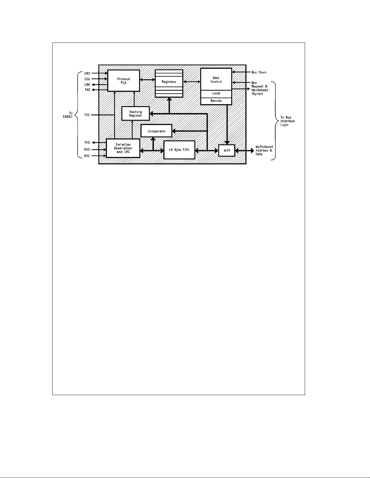
The DP8390 Core logic,
Deserializer which is controlled by the Protocol PLA, DMA
Control, FIFO, Address Comparator, Multicast Hashing Register. The DP8390 core implements all of the IEEE 802.3
Media access control functions for the AT/LANTIC Controller, and interfaces to the internal ENDEC (on the left of the
block diagram) and also interfaces to the Bus Interface and
memory support bus via a number of address, data and control signal (and the right side of the block diagram). The
following sections describe the functions of the DP8390
core.
Receive Deserializer
The Receive Deserializer is activated when the input signal
Carrier Sense is asserted to allow incoming bits to be shifted into the shift register by the receive clock. The serial
receive data is also routed to the CRC generator/checker.
The Receive Deserializer includes a synch detector which
detects the SFD (Start of Frame Delimiter) to establish
where byte boundaries within the serial bit stream are located. After every eight receive clocks, the byte wide data is
transferred to the 16-byte FlFO and the Receive Byte Count
is incremented. The first six bytes after the SFD are
checked for valid comparison by the Address Recognition
Logic. If the Address Recognition Logic does not recognize
the packet, the FlFO is cleared.
CRC Generator/Checker
During transmission, the CRC logic generates a local CRC
field for the transmitted bit sequence. The CRC encodes all
fields after the synch byte. The CRC is shifted out MSB first
following the last transmit byte. During reception the CRC
logic generates a CRC field from the incoming packet. This
local CRC is serially compared to the incoming CRC appended to the end of the packet by the transmitting node. If
the local and received CRC match, a specific pattern will be
generated and decoded to indicate no data errors. Transmission errors result in different patterns and are detected,
resulting in rejection of a packet.
Figure 12
, contains the Serializer/
16
Page 17
4.0 Functional Description (Continued)
FIGURE 12. DP8390 Controller Core Simplified Block Diagram
Transmit Serializer
The Transmit Serializer reads parallel data from the FIFO
and serializes it for transmission. The serializer is clocked by
the transmit clock generated internally. The serial data is
also shifted into the CRC generator/checker. At the beginning of each transmission, the Preamble and Synch Generator append 62 bits of 1,0 preamble and a 1,1 synch pattern. After the last data byte of the packet has been serialized the 32-bit FCS (Frame Check Sequence) field is shifted
directly out of the CRC generator. In the event of a collision
the Preamble and Synch generator is used to generate a
32-bit JAM pattern of all 1’s.
Comparator-address Recognition Logic
The address recognition logic compares the Destination Address Field (first 6 bytes of the received packet) to the Physical address registers stored in the Address Register Array.
If any one of the six bytes does not match the pre-programmed physical address, the Protocol Control Logic rejects the packet. All multicast destination addresses are filtered using a hashing technique. (See register description.)
If the multicast address indexes a bit that has been set in
the filter bit array of the Multicast Address Register Array
the packet is accepted, otherwise it is rejected by the Protocol Control Logic. Each destination address is also checked
for all 1’s which is the reserved broadcast address.
FIFO and Packet Data Operations
OVERVIEW
To accommodate the different rates at which data comes
from (or goes to) the network and goes to (or comes from)
the packet buffer memory, the AT/LANTIC Controller contains a 16-byte FIFO for buffering data between the media
and the buffer RAM located on the memory support bus.
The FIFO threshold is programmable, allowing filling (or
emptying) the FIFO at different rates. When the FIFO has
filled to its programmed threshold, the local DMA channel
transfers these bytes (or words) into local memory (via the
TL/F/11498– 9
memory bus). It is crucial that the local DMA is given access
to the bus within a minimum bus latency time; otherwise a
FIFO underrun (or overrun) occurs.
FIFO underruns or overruns are caused when a local DMA
request is issued while an ISA bus access is current and the
ISA cycle takes longer to complete than the local DMA’s
tolerable latency. This tolerable latency depends on the
FIFO threshold, whether it is in byte or word wide mode and
the speed of the DMA clock (BSCLK frequency). Note that
this refers to standard ISA cycles NOT those where the
CHRDY is deasserted extending the cycle.
FIFO THRESHOLD DETECTION
To assure that there is no overwriting of data in the FIFO,
the FIFO logic flags a FIFO overrun as the 13th byte is
written into the FIFO, effectively shortening the FIFO to 13
bytes. The FIFO logic also operates differently in Byte Mode
and in Word Mode. In Byte Mode, a threshold is indicated
when the n
a
1 byte has entered the FIFO; thus, with an 8
byte threshold, the AT/LANTIC Controller issues a request
to the buffer RAM when the 9th byte has entered the FIFO,
making the effective threshold 9 bytes. For Word Mode, the
request is not generated until the n
a
2 bytes have entered
the FIFO. Thus, with a 4 word threshold (equivalent to 8
byte threshold), a request to the buffer RAM is issued when
the 10th byte has entered the FIFO, making the effective
threshold 10 bytes.
TOLERABLE LATENCY CALCULATION
To prevent a FIFO overrun a byte (or word) of data must be
removed from the FIFO before the 13th byte is written.
Therefore the worst case tolerable latency is the time from
the effective threshold being reached to the time the 13th
byte is written minus the time taken to load the first byte (or
word) of data to the FIFO during a local DMA burst (8
BSCLKs).
tolerable latency
e
((overrunbeffective) threshold
c
time to transfer byte on network)
b
time to fill 1st FIFO location
17
Page 18

4.0 Functional Description (Continued)
For the case of a 4 word threshold using a 20 MHz BSCLK:
tolerable latency
To prevent a FIFO underrun a byte (or word) of data must
be added from the FIFO before the last byte is removed.
Therefore the worst case tolerable latency is the time from
the effective threshold being reached to the time the last
byte is removed minus the time taken to load the first byte
(or word) of data to the FIFO during a local DMA burst (8
BSCLKs).
tolerable latency
For the case of a 4 word threshold using a 20 MHz BSCLK:
tolerable latencye(4c800)b(8c50) ns
The worst case latency, either overrun or underrun, ultimately limits the overall latency that the AT/LANTIC Controller can tolerate. If the standard ISA cycles are shorter
than the worst case latency then no FIFO overruns or underruns will occur.
BEGINNING OF RECEIVE
At the beginning or reception, the AT/LANTIC Controller
stores entire Address field of each incoming packet in the
FIFO to determine whether the packet matches its Physical
Address Registers or maps to one of its Multicast Registers.
This causes the FIFO to accumulate 8 bytes.
Furthermore, there are some synchronization delays in the
DMA PLA. Thus, the actual time that a request to access
the buffer RAM is asserted from the time the Start of Frame
Delimiter (SFD) is detected is 7.8 ms. This operation affects
the bus latencies at 2 byte and 4 byte thresholds during the
first receive request since the FIFO must be filled to 8 bytes
(or 4 words) before issuing a request to the buffer RAM.
END OF RECEIVE
When the end of a packet is detected by the ENDEC module, the AT/LANTIC Controller enters its end of packet processing sequence, emptying its FIFO and writing the status
information at the beginning of the packet. The AT/LANTIC
Controller holds onto the memory bus for the entire sequence. The longest time that local DMA will hold the buffer
RAM occurs when a packet ends just as the AT/LANTIC
Controller performs its last FIFO burst. The AT/LANTIC
Controller, in this case, performs a programmed burst transfer followed by flushing the remaining bytes in the FIFO, and
completed by writing the header information to the buffer
memory. The following steps occur during this sequence.
e
((13b10)c800)b(8c50) ns
e
2 ms
e
(threshold
c
time to transfer byte on network)
b
time to fill 1st FIFO location
e
2.8 ms
1. AT/LANTIC Controller issues request to access the
RAM because the FIFO threshold has been reached.
2. During the burst, packet ends, resulting in the request
being extended.
3. AT/LANTIC Controller flushes remaining bytes from
FIFO.
4. AT/LANTIC Controller performs internal processing to
prepare for writing the header.
5. AT/LANTIC Controller writes 4-byte (2-word) header
6. AT/LANTIC Controller de-asserts access to the buffer
RAM.
BEGINNING OF TRANSMIT
Before transmitting, the AT/LANTIC Controller performs a
prefetch from memory to load the FIFO. The number of
bytes prefetched is the programmed FIFO threshold. The
next request to the buffer RAM is not issued until after the
AT/LANTIC Controller actually begins transmitting data, i.e.,
after SFD.
READING THE FIFO
If the FIFO is read during normal operation the AT/LANTIC
Controller will ‘‘hang’’ the ISA bus by deasserting CHRDY
and never asserting it. The FIFO should only be read during
loopback diagnostics, when it will operate normally.
PROTOCOL PLA
The Protocol PLA is responsible for implementing the IEEE
802.3 protocol, including collision recovery with random
backoff. The Protocol PLA also formats packets during
transmission and strips preamble and synch during reception.
DMA AND BUFFER CONTROL LOGIC
The DMA and Buffer Control Logic is used to control two
16-bit DMA channels. During reception, the Local DMA
stores packets in a receive buffer ring, located in buffer
memory. During transmission the Local DMA uses programmed pointer and length registers to transfer a packet
from local buffer memory to the FIFO.
A second DMA channel is used when the AT/LANTIC Controller is used in I/O Port mode. This DMA is used as a slave
DMA to transfer data between the local buffer memory and
the host system. The Local DMA and Remote DMA are internally arbitrated, with the Local DMA channel having highest priority. Both DMA channels use a common external bus
clock to generate all required bus timing. External arbitration
is performed with a standard bus request, bus acknowledge
handshake protocol.
In the shared memory mode the Remote DMA is not used,
because in this mode the system has direct read/write access to the buffer RAM.
18
Page 19
4.0 Functional Description (Continued)
4.8 TWISTED PAIR INTERFACE MODULE
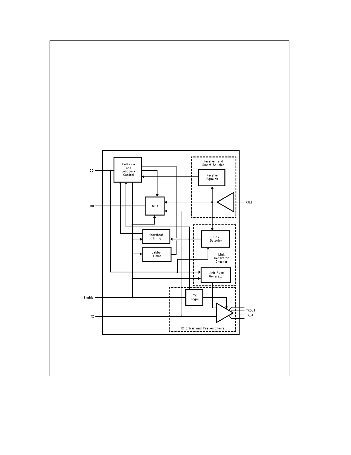
The TPI consists of five main logical functions:
a) The Receiver/Smart Squelch, responsible for determin-
ing when valid data is present on the differential receive
inputs (RXI
b) The Collision function checks for simultaneous transmis-
sion and reception of data on the TXO
c) The Link Detector/Generator checks the integrity of the
cable connecting the two twisted pair MAUs.
d) The Jabber disables the transmitter if it attempts to
transmit a longer than legal packet.
e) The TX Driver and Pre-emphasis transmits Manchester
encoded data to the twisted pair network via the summing resistors and transformer/filter.
g
) and receiving the data.
g
and RXIgpins.
Receiver and Smart Squelch
The AT/LANTIC Controller implements an intelligent receive squelch on the RXI
g
differential inputs to ensure that
impulse noise on the receive inputs will not be mistaken for
a valid signal.
The squelch circuitry employs a combination of amplitude
and timing measurements to determine the validity of data
on the twisted pair inputs. There are two voltage level options for the smart squelch. One mode, 10BASE-T mode,
uses levels that meet the 10BASE-T specification. The second mode, reduced squelch mode, uses a lower squelch
threshold level, and can be used in longer cable applications where smaller signal levels may be applied. The
squelch level mode can be selected in the AT/LANTIC Controller configuration registers.
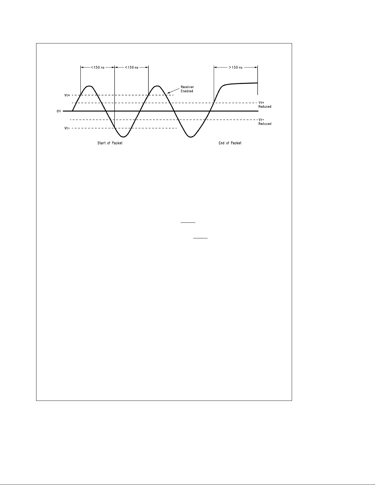
Figure 14
shows the operation of the smart squelch in
10BASE-T mode.
FIGURE 13. Twisted Pair Interface Module Block Diagram
19
TL/F/11498– 10
Page 20
4.0 Functional Description (Continued)
FIGURE 14. Twisted Pair Squelch Waveform
The signal at the start of packet is checked by the smart
squelch and any pulses not exceeding the squelch level
(either positive or negative, depending upon polarity) will be
rejected. Once this first squelch level is overcome correctly
the opposite squelch level must then be exceeded within
150 ns later. Finally the signal must exceed the original
squelch level within a further 150 ns to ensure that the input
waveform will not be rejected. The checking procedure results in the loss of typically three bits at the beginning of
each packet.
Only after all these conditions have been satisfied will a
control signal be generated to indicate to the remainder of
the circuitry that valid data is present. At this time the smart
squelch circuitry is reset.
In the reduced squelch mode the operation is identical except that the lower squelch levels shown in
Figure 14
are
used.
Valid data is considered to be present until either squelch
level has not been generated for a time longer than 150 ns,
indicating End of Packet. Once good data has been detected the squelch levels are reduced to minimize the effect of
noise causing premature End of Packet detection.
Collision
A collision is detected by the TPI module when the receive
and transmit channels are active simultaneously. If the TPI
is receiving when a collision is detected it is reported to the
controller immediately. If, however, the TPI is transmitting
when a collision is detected the collision is not reported until
seven bits have been received while in the collision state.
This prevents a collision being reported incorrectly due to
noise on the network. The signal to the controller remains
for the duration of the collision.
Approximately 1 ms after the transmission of each packet a
signal called the Signal Quality Error (SQE) consisting of
typically 10 cycles of 10 MHz is generated. This 10 MHz
signal, also called the Heartbeat, ensures the continued
functioning of the collision circuitry.
TL/F/11498– 11
Link Detector/Generator
The link generator is a timer circuit that generates a link
pulse as defined by the 10 Base-T specification that will be
generated by the transmitter section. The pulse which is
100 ns wide is transmitted on the TXO
a
output, every
16 ms, in the absence of transmit data.
The pulse is used to check the integrity of the connection to
the remote MAU. The link detection circuit checks for valid
pulses from the remote MAU and if valid link pulses are not
received the link detector will disable the transmit, receive
and collision detection functions.
The GDLNK
output can directly drive a LED to show that
there is a good twisted pair link. For normal conditions the
LED will be on. The link integrity function can be disabled by
setting the GDLNK
bit of Configuration Register B.
Jabber
The jabber timer monitors the transmitter and disables the
transmission if the transmitter is active for greater than
26 ms. The transmitter is then disabled for the whole time
that the Endec module’s internal transmit enable is asserted. This signal has to be deasserted for approximately
750 ms (the unjab time) before the Jabber re-enables the
transmit outputs.
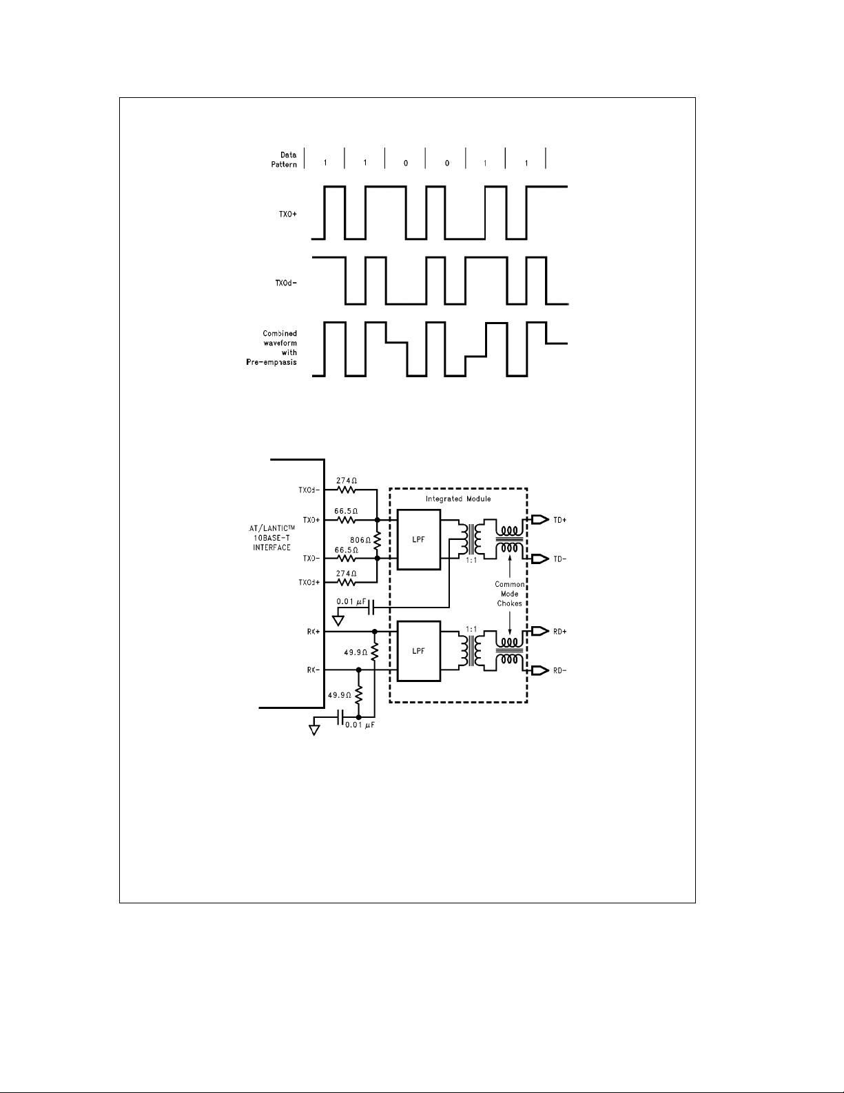
Transmitter
The transmitter consists of four signals, the true and compliment Manchester encoded data (TXO
delayed by 50 ns (TXOd
These four signals are resistively combined TXOawith
b
TXOd
and TXObwith TXOda. This is known as digital
g
)
g
) and these signals
pre-emphasis and is required to compensate for the twisted
pair cable which acts like a low pass filter causing greater
attenuation to the 10 MHz (50 ns) pulses of the Manchester
encoded waveform than the 5 MHz (100 ns) pulses.
An example of how these siqnals are combined is shown in
the following diagram.
20
Page 21
4.0 Functional Description (Continued)
FIGURE 15. Typical Summed Transmit Waveform
The signal with pre-emphasis shown above is generated by resistively combining TXO
compliment is passed to the transmit filter.
FIGURE 16. External Circuitry to Connect AT/LANTIC Controller to Twisted Pair Cable
TL/F/11498– 12
a
and TXOdb. This signal along with its
TL/F/11498– 13
21
Page 22
4.0 Functional Description (Continued)
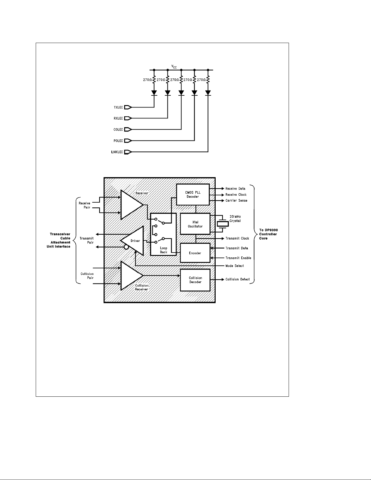
FIGURE 17. Typical AT/LANTIC Controller LED Connection
TL/F/11498– 15
FIGURE 18. Encoder/Decode Block Diagram
22
TL/F/11498– 14
Page 23
4.0 Functional Description (Continued)
Status Information
Status information is provided by the AT/LANTIC Controller
on the RXLED, TXLED, COLED and POL outputs as described in the pin description table. These outputs are suitable for driving status LED’s as shown in
puts are open drain.
Recommended integrated Filter-Transformer-choke modules:
1. Pulse Engineering PE65424
2. Valor FL1012 or FL1030.
4.9 ENCODER/DECODER (ENDEC) MODULE
The ENDEC consists of four main logical blocks:
a. The oscillator generates the 10 MHz transmit clock sig-
nal for system timing.
b. The Manchester encoder accepts NRZ data from the
controller, encodes the data to Manchester, and transmits the data differentially to the transceiver, through the
differential transmit driver.
c. The Manchester decoder receives Manchester data from
the transceiver, converts it to NRZ data and clock pulses, and sends it to the controller.
d. The collision translator indicates to the controller the
presence of a valid 10 MHz collision signal to the PLL.
Oscillator
The oscillator is controlled by a 20 MHz parallel resonant
crystal connected between X1 and X2 or by an external
clock on X1. The 20 MHz output of the oscillator is divided
by 2 to generate the 10 MHz transmit clock for the controller. The oscillator also provides internal clock signals to the
encoding and decoding circuits.
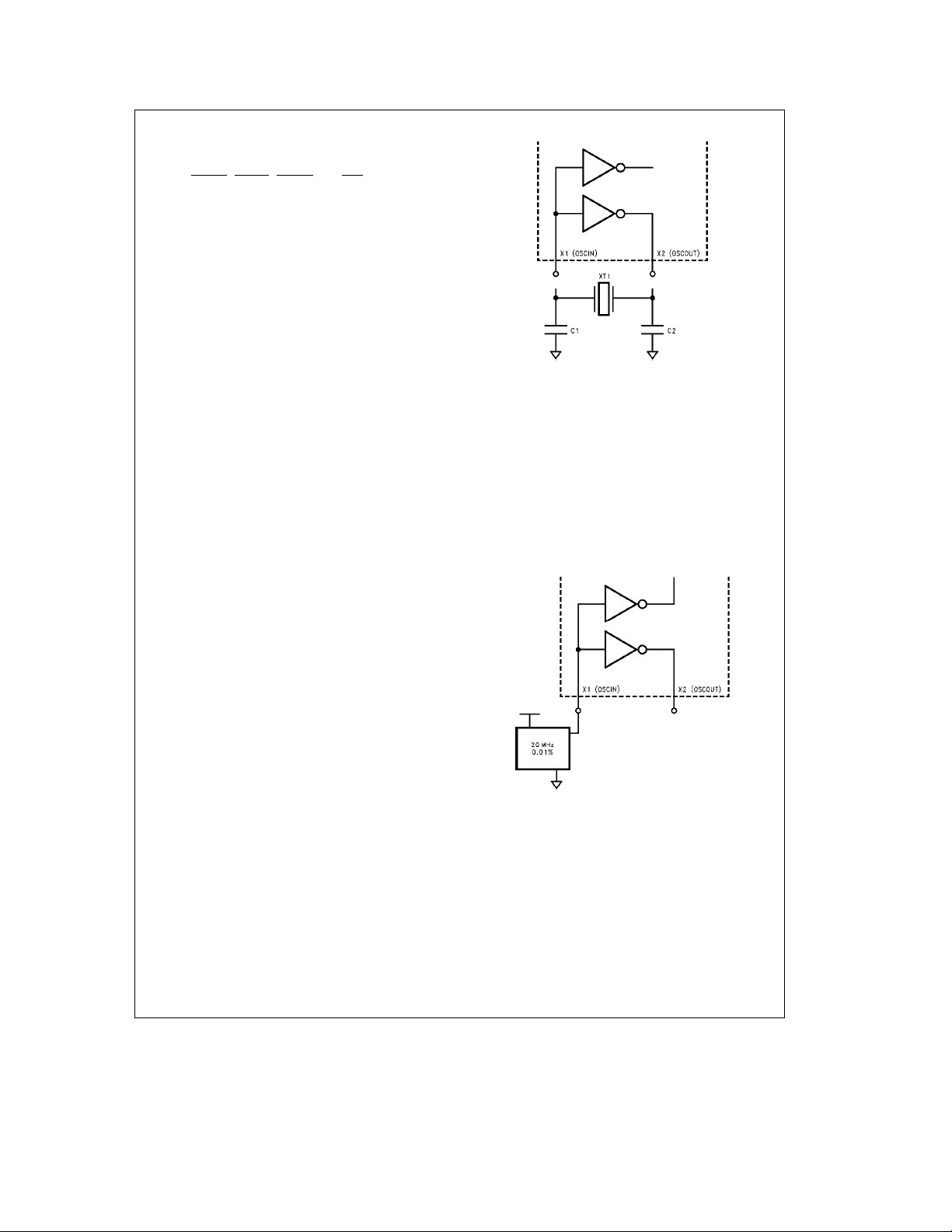
CRYSTAL OPERATION
If the crystal used with the internal oscillator circuit is not
properly selected, the AT/LANTIC Controller oscillator may
not reliably start oscillation under all conditions.
If this occurs, it could be deceiving to a designer, since his
prototypes may work fine. However, when the designer
does qualification testing or starts production, he may encounter a higher than expected board yield loss due to the
oscillator not starting. The AT/LANTIC Controller’s oscillator circuit clocks the Encoder-Decoder logic. The
AT/LANTIC Controller’s oscillator also clocks the twisted
pair interface block. If the oscillator does not start, the
AT/LANTIC Controller will not be able to transmit or receive.
If a crystal is connected to the AT/LANTIC Controller, it is
recommended that the circuit shown in
and that the components used meet the following:
Crystal XT1: AT cut parallel resonant crystal
Series Resistance:
Specified Load Capacitance:
Accuracy: 0.005% (50 ppm)
Typical Load: 50 mW–75 mW
The recommended values for capacitors C1 and C2 are
26 pF minus the board capacitance on that pin. Therefore if
both X1 and X2 have 4 pF of board capacitance, then a
22 pF capacitor should be used.
According to the IEEE 802.3 standard, the entire oscillator
circuit (crystal and amplifier) must be accurate to 0.01%.
When using a crystal, the X2 pin is not guaranteed to provide a TTL compatible logic output, and should not be used
Figure 17
. All out-
Figure 19
s
25X
s
be used
20 pF
FIGURE 19. Crystal Connection to AT/LANTIC
Controller (see text for component values)
to drive external standard logic. If additional logic needs to
be driven, then an external oscillator should be used, as
described in the following section.
OSCILLATOR MODULE OPERATION
If the designer wishes to use a crystal clock oscillator, one
that provides the following should be employed:
1. TTL or CMOS output with a 0.01% frequency tolerance
2. 40% – 60% duty cycle
The circuit is shown in
Figure 20
. When using a clock oscillator it is recommended that the designer connect the oscillator output to the X1 pin and leave the X2 pin floating.
FIGURE 20. AT/LANTIC Controller
Connection for Oscillator Module
Manchester Encoder and Differential Driver
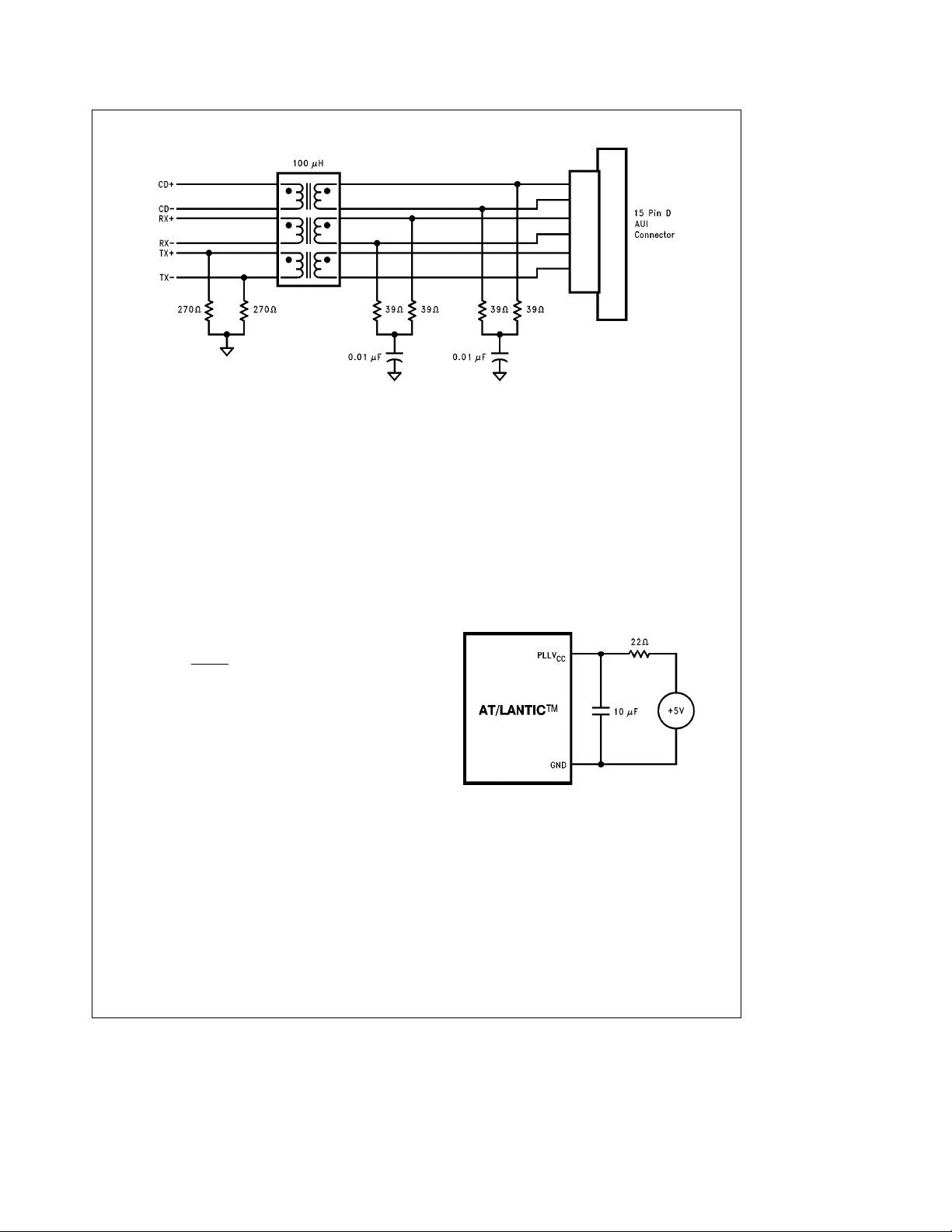
The differential transmit pair, on the secondary of the employed transformer, drives up to 50 meters of twisted pair
AUI cable. These outputs are source followers which require
two 270X pull-down resistors to ground (see
The AT/LANTIC Controller allows full-step to be compatible
with IEEE 802.3. Transmit
a
and Transmitbare equal in the
Figure 21
idle state, providing zero differential voltage to operate with
transformer coupled loads.
Manchester Decoder
The decoder consists of a differential receiver and a PLL to
separate a Manchester encoded data stream into internal
23
TL/F/11498– 16
TL/F/11498– 17
).
Page 24
4.0 Functional Description (Continued)
FIGURE 21. Connection from AT/LANTIC Controller’s AUI Port to the AUI Connector
clock signals and data. The differential input must be externally terminated with two 39X resistors connected in series
if the standard 78X transceiver drop cable is used, in thin
Ethernet applications, these resistors are optional. To prevent noise from falsely triggering the decoder, a squelch
circuit at the input rejects signals with levels less than
b
175 mV. Data becomes valid typically within 6 bit times.
The AT/LANTIC Controller may tolerate bit jitter up to 20 ns
in the received data. The decoder detects the end of a
frame when no more mid-bit transitions are detected.
Collision Translator
When in AUI Mode, the Ethernet transceiver (DP8392 CTl)
detects a collision, it generates a 10 MHz signal to the differential collision inputs (CD
g
) of the AT/LANTIC Controller. When these inputs are detected active, the AT/LANTIC
Controller uses this signal to back off its current transmission and reschedule another one.
In this mode the COLED
output will indicate when the CD
lines are active during activity on the network. This means it
will correctly indicate any collision on the network, but will
not be lit for heartbeat or if there is no cable connected.
The collision differential inputs are terminated the same way
as the differential receive inputs. The squelch circuitry is
also similar, rejecting pulse levels less than
PLL V
Power Supply Consideration
CC
b
175 mV.
The PLL VCCpin is thea5V power supply for the phase
lock loop (PLL) of the ST-NIC ENDEC unit. Since this is an
TL/F/11498– 19
analog circuit, excessive noise on the PLL V
fect the performance of the PLL. This noise, if in the
pin can af-
CC
10 kHz–400 kHz range, can reduce the jitter performance of
the ENDEC, resulting in missing packets or CRC errors.
If the power supply noise is causing significant packet reception error, a low pass filter could be added to reduce the
power supply noise and hence improve the jitter performance. Standard analog design techniques should be utilized
when laying out the power supply traces on the board. If the
digital power supply is used, it may be desirable to add a
one pole RC filter (designed to have a cut-off frequency of
1 kHz) as shown in
ance. The PLL V
across the resister is less than 90 mV, which will not affect
Figure 4
only draws 3 mA – 4 mA so the voltage
CC
to improve the jitter perform-
the PLL’s operation.
g
TL/F/11498– 18
FIGURE 22. Filtering Power Supply Noise
24
Page 25

5.0 Register Descriptions
5.1 CONFIGURATION REGISTERS
These registers are used to configure the operation of the AT/LANTIC Controller typically after power up. These registers
control the configuration of bus interface, setting options like interrupt selection, I/O base address, and other specific modes.
MODE CONFIGURATION REGISTER A
To prevent any accidental writes of this register it is ‘‘hidden’’ behind a previously unused register. Register 0AH in the
AT/LANTIC Controller’s Page 0 of registers was previously reserved on a read. Now Configuration Register A can be read at
that address and can be written to by following a read to 0AH with a write to 0AH. If any other AT/LANTIC Controller register
accesses take place between the read and the write then the write to 0AH will access the Remote Byte Count Register 0.
76543210
MEMIO FREAD INT2 INT1 INT0 IOAD2 IOAD1 IOAD0
Bits Symbols Function
0–2 IOAD0 – I/O ADDRESS: These three bits determine the base I/O address of the AT/LANTIC Controller, within
IOAD2
3–5 INT0 – INTERRUPT LINE USED: There are two interrupt modes which can be enabled by setting bit 5 of
INT2
6 FREAD FAST READ: When this bit is set high the AT/LANTIC Controller, in I/O mode, will begin the next port
7 MEMIO MEMORY OR I/O MODE: If this bit is set high then the AT/LANTIC Controller is in shared memory
the system’s I/O map. The AT/LANTIC Controller occupies 20H bytes of the system’s address space.
0 0 0 0300H
0 0 1 Software (Note 1)
0 1 0 0240H
0 1 1 0280H
1 0 0 02C0H
1 0 1 0320H
1 1 0 0340H
1 1 1 0360H
Note 1: When 001 is selected the AT/LANTIC controller will not respond to any I/O Addresses, but will allow 4 consecutive writes to 278H to
write these three bits of this register. This sequence will only operate once after a power-on reset. This mode allows the AT/LANTIC
Controller to be configured via software without conflicting with other peripherals.
Configuration Register C to the appropriate level.
DIRECT DRIVE MODE: In this mode an interrupt output pin will be driven active on a valid interrupt
condition. Only one pin may be driven, the other three will remain at TRI-STATE
. The pin driven is
É
determined by the value in this register.
Bit 5 Bit 4 Bit 3 Interrupt
X 0 0 INT0
X 0 1 INT1
X 1 0 INT2
X 1 1 INT3
CODED OUTPUT MODE: In this mode INT3 is the active interrupt output while pins INT0 to INT2 are
programmable outputs reflecting the values on bits 3 to 5.
fetch before the current IORD has completed. In slow ISA systems this may cause the data in the port
to be overwritten before the ISA cycle has been completed.
mode. If it is set low it is in I/O mode.
25
Page 26

5.0 Register Descriptions (Continued)
Mode Configuration Register B
To prevent any accidental writes of this register it is ‘‘hidden’’ behind a previously unused register. Register 0BH in the
AT/LANTIC Controller’s Page 0 of registers was previously reserved on a read. Now Configuration Register B can be read at
that address and can be written to by following a read to 0BH with a write to 0BH. If any other AT/LANTIC Controller register
accesses take place between the read and the write then the write to 0BH will access the Remote Byte Count Register 1. Care
should be taken when writing to this register as GDLINK and BE are not simple read/write bits, e.g., the user cannot
change the physical layer by reading B, or-ing the returned value with the bits to be set, and writing this value to B. This could
inadvertently disable link integrity generation and clear a bus error indication before it was noted.
7654 3 210
EELOAD BPWR BE CHRDY IO16CON GDLINK PHYS1 PHYS0
Bits Symbols Function
0–1 PHYS0 – PHYSICAL LAYER INTERFACE: These 2 bits determine which type of physical interface the AT/LANTIC
PHYS1
2 GDLNK GOOD LINK: Whena1iswritten to this bit the link test pulse generation and integrity checking is disabled.
3 IO16CON IO16 CONTROL: When this bit is set high the AT/LANTIC Controller generates IO16 after IORD or IOWR go
4 CHRDY CHRDY FROM IORD OR IOWR OR FROM BALE: When this bit is low the AT/LANTIC Controller will generate
5BE BUS ERROR: This bit shows that the AT/LANTIC Controller has detected a bus error condition. This will go
6 BPWR BOOT PROM WRITE: When this bit is low no write cycles are generated to the boot PROM.
7 EELOAD EEPROM LOAD: Writinga1tothis bit enables the EEPROM load algorithm as detailed in Section 4. This bit
Controller is using. The 2 TPI interfaces use twisted pair outputs and inputs, while the other 2 interfaces use the
AUI outputs and inputs. In 10BASE5 mode the THIN output pin is driven low, in 10BASE2 mode it is driven high.
This can be used to enable the DC–DC converter required by the 10BASE2 specification to provide electrical
isolation. The Non spec TPI mode is a twisted pair mode with reduced receive squelch levels. This allows the
use of longer cable lengths than specified in the twisted pair specification, or use of cable with higher losses.
0 0 TPI (10BASE-T Compatible Squelch Level)
0 1 Thin Ethernet (10BASE2)
1 0 Thick Ethernet (10BASE5) (AUI Port)
1 1 TPI (Reduced Squelch Level)
When this bit is read it will indicate link status, reflecting the value shown on the LED output. It is 0 if the
AT/LANTIC Controller is in AUI mode or if link testing is enabled and the link integrity is bad (i.e., the twisted
pair link has been broken). It is 1 if the AT/LANTIC Controller is in TPI mode, link integrity checking is enabled
and the link integrity is good (i.e., the twisted pair link has not been broken) or if the link testing is disabled.
active. If low this output is generated only on address decode.
CHARDY after the command strobe. When high it will generate it after BALE goes high.
high if the AT/LANTIC Controller attempts to insert wait states into a system access and the system terminates
the cycle without inserting the wait states. Writing a one to this bit clears it to zero. Writing a zero has no effect.
should not be configured to be high, either from switches or an EEPROM.
26
Page 27

5.0 Register Descriptions (Continued)
Hardware Configuration Register C
This register is configured during a RESET and can not be accessed by software.
7 6 5 4 3210
SOFEN CLKSEL INTMOD COMP BPS3 BPS2 BPS1 BPS0
Bits Symbols Function
0–3 BPS0b3 BOOT PROM SELECT: Selects address at which boot PROM begins and the size. When the system reads
4 COMP COMPATIBLE: This bit determines if the AT/LANTIC Controller’s memory and I/O maps are compatible with
5 INTMOD INTERRUPT MODE: When this bit is low the AT/LANTIC Controller is in Direct Drive interrupt mode. When it is
6 CLKSEL CLOCK SELECT: If this bit is low the NIC core is clocked by the 20 MHz. If this bit is high the NIC core is
7 SOFEN SOFTWARE ENABLE: If this bit is set low then the user can program configuration registers A and B in
within the selected memory area AT/LANTIC Controller reads the data in through MSD0–7 and drives it onto
the system data bus. The following are valid addresses and sizes:
Bit 3 Bit 2 Bit 1 Bit 0 Address Size (I/O / Shared Mem.)
0 0 0 X X No boot PROM
0 0 1 0 0C000H 8k/16k
0 0 1 1 0C400H 8k/16k
0 1 0 0 0C800H 8k/16k
0 1 0 1 0CC00H 8k/16k
0 1 1 0 0D000H 8k/16k
0 1 1 1 0D400H 8k/16k
1 0 0 0 0D800H 8k/16k
1 0 0 1 0DC00H 8k/16k
1 0 1 0 0C000H 32k/32k
1 0 1 1 0C800H 32k/32k
1 1 0 0 0D000H 32k/32k
1 1 0 1 0D800H 32k/32k
1 1 1 0 0C000H 64k/64k
1 1 1 1 0D000H 64k/64k
the EtherCard PLUS and Novell boards or if they use the full 64k address space available to the NIC. A low level
indicates compatible mode.
high Coded Output interrupt mode is used.
clocked by the signal on the BSCLK pin.
software. If this bit is set high then the configuration registers are not accessible. If EECONFIG is high, the
configuration from the switches will be overwritten by the configuration from the EEPROM even if this bit is
pulled high.
27
Page 28

5.0 Register Descriptions (Continued)
5.2 SHARED MEMORY MODE CONTROL REGISTERS
The following tables describe the functionality of the two control registers and the 8/16 detection registers.
Shared Memory AT Detect Register (Read only)
76543210
xxxxxxxATDET
Bits Symbols Function
D0 ATDET ATDET: This bit shows the value on the DWID pin and can be read by software to determine whether the
Shared Memory Control Register 1
Bits Symbols Function
D0-D5 A13– A18 A13–18: Lower part of the address register used to determine the position of the AT/LANTIC
D6 MEME MEMORY ENABLE: Enables external memory accesses when held high. This bit will power up low,
D7 RESET RESET: Resets NIC core of AT/LANTIC Controller.
AT/LANTIC Controller is operating in an 8- or 16-bit slot. When this bit is read as a 1 the AT/LANTIC Controller
is in a 16-bit slot (PC-AT system bus) and when read asa0itisinan8-bit slot.
76543210
RESET MEME A18 A17 A16 A15 A14 A13
Controller’s memory within the system memory map.
so the user must program the base memory address and set this bit high to enable the memory into
the system’s memory map.
Shared Memory Control Register 2
765 43210
8/16 MEMW Unused LA23 LA22 LA21 LA20 LA19
Bits Symbols Function
D0–D4 LA19 –LA23 LA19 – 23: Upper part of the address register used to determine the position of the AT/LANTIC
Controller’s memory within the system memory map.
D5 UNUSED
D6 MEMW MEMORY WIDTH: Sets width of external memory. When set low external memory is accessed as
byte wide, so only 8 kbytes of memory are available. When set high external memory is accessed
as word wide, so 16 kbytes are available. In non-compatible mode up to 64 kbytes of external
memory is allowed when this bit is set high, or 32 kbytes when low. When bit 7 is set high this bit
must also be set high.
D7 8/16 8/16-BIT: Allows 16-bit system accesses to external memory when set high. When low only 8-bit
accesses are allowed. When high the generation of the M16 output is allowed.
28
Page 29

5.0 Register Descriptions (Continued)
5.3 NIC CORE REGISTERS
All registers are 8-bit wide and mapped into two pages which are selected in the Command Register (PS0, PS1). Pins SA0 – SA3
are used to address registers within each page. Page 0 registers are those registers which are commonly accessed during
AT/LANTIC Controller operation while page 1 registers are used primarily for initialization. The registers are partitioned to avoid
having to perform two write/read cycles to access commonly used registers.
TL/F/11498– 20
FIGURE 23. NIC Core Register Mapping
29
Page 30

5.0 Register Descriptions (Continued)
Register Assignments
Page 0 Address Assignments (PS1
SA0–SA3 RD WR
00H Command (CR) Command (CR)
01H Current Local DMA Page Start Register
Address 0 (CLDA0) (PSTART)
02H Current Local DMA Page Stop Register
Address 1 (CLDA1) (PSTOP)
03H Boundary Pointer Boundary Pointer
(BNRY) (BNRY)
04H Transmit Status Transmit Page Start
Register (TSR) Address (TPSR)
05H Number of Collisions Transmit Byte Count
Register (NCR) Register 0 (TBCR0)
06H FIFO (FIFO) Transmit Byte Count
07H Interrupt Status Interrupt Status
Register (ISR) Register (ISR)
08H Current Remote DMA Remote Start Address
Address 0 (CRDA0) Register 0 (RSAR0)
09H Current Remote DMA Remote Start Address
Address 1 (CRDA1) Register 1 (RSAR1)
0AH Reserved Remote Byte Count
0BH Reserved Remote Byte Count
0CH Receive Status Receive Configuration
Register (RSR) Register (RCR)
0DH Tally Counter 0 Transmit Configuration
(Frame Alignment Register (TCR)
Errors) (CNTR0)
0EH Tally Counter 1 Data Configuration
(CRC Errors) Register (DCR)
(CNTR1)
0FH Tally Counter 2 Interrupt Mask
Missed Packet Register (IMR)
Errors) (CNTR2)
e
0, PS0e0)
Register 1 (TBCR1)
Register 0 (RBCR0)
Register 1 (RBCR1)
30
Page 31

5.0 Register Descriptions (Continued)
Page 1 Address Assignments (PS1
SA0–SA3 RD WR
00H Command (CR) Command (CR)
01H Physical Address Physical Address
Register 0 (PAR0) Register 0 (PA R0)
02H Physical Address Physical Address
Register 1 (PAR1) Register 1 (PA R1)
03H Physical Address Physical Address
Register 2 (PAR2) Register 2 (PAR2)
04H Physical Address Physical Address
Register 3 (PAR3) Register 3 (PAR3)
05H Physical Address Physical Address
Register 4 (PAR4) Register 4 (PAR4)
06H Physical Address Physical Address
Register 5 (PAR5) Register 5 (PAR5)
07H Current Page Current Page
Register (CURR) Register (CURR)
08H Multicast Address Multicast Address
Register 0 (MAR0) Register 0 (MAR0)
09H Multicast Address Multicast Address
Register 1 (MAR1) Register 1 (MAR1)
0AH Multicast Address Multicast Address
Register 2 (MAR2) Register 2 (MAR2)
0BH Multicast Address Multicast Address
Register 3 (MAR3) Register 3 (MAR3)
0CH Multicast Address Multicast Address
Register 4 (MAR4) Register 4 (MAR4)
0DH Multicast Address Multicast Address
Register 5 (MAR5) Register 5 (MAR5)
0EH Multicast Address Multicast Address
Register 6 (MAR6) Register 6 (MAR6)
0FH Multicast Address Multicast Address
Register 7 (MAR7) Register 7 (MAR7)
e
0, PS0e1)
31
Page 32

5.0 Register Descriptions (Continued)
Page 2 Address Assignments (PS1
SA0–SA3 RD WR
00H Command (CR) Command (CR)
01H Page Start Register Current Local DMA
02H Page Stop Register Current Local DMA
03H Remote Next Packet Remote Next Packet
04H Transmit Page Start Reserved
05H Local Next Packet Local Next Packet
06H Address Counter Address Counter
07H Address Counter Address Counter
08H Reserved Reserved
09H Reserved Reserved
0AH Reserved Reserved
0BH Reserved Reserved
0CH Receive Configuration Reserved
0DH Transmit Reserved
OEH Data Configuration Reserved
0FH Interrupt Mask Reserved
Note: Page 2 registers should only be accessed for diagnostic purposes. They should not
be modified during normal operation.
Page 3 should never be modified.
(PSTART) Address 0 (CLDA0)
(PSTOP) Address 1 (CLDA1)
Pointer Pointer
Address (TPSR)
Pointer Pointer
(Upper) (Upper)
(Lower) (Lower)
Register (RCR)
Configuration
Register (TCR)
Register (DCR)
Register (IMR)
e
1, PS0e0)
32
Page 33

5.0 Register Descriptions (Continued)
COMMAND REGISTER (CR) 00H (READ/WRITE)
The Command Register is used to initiate transmissions, enable or disable Remote DMA operations and to select register
pages. To issue a command the microprocessor sets the corresponding bit(s) (RD2, RDl, RD0, TXP). Further commands may be
overlapped, but with the following rules: (1) If a transmit command overlaps with a remote DMA operation, bits RD0, RD1, and
RD2 must be maintained for the remote DMA command when setting the TXP bit. Note, if a remote DMA command is re-issued
when giving the transmit command, the DMA will complete immediately if the remote byte count register has not been re-initialized. (2) If a remote DMA operation overlaps a transmission, RD0, RD1, and RD2 may be written with the desired values and a
‘‘0’’ written to the TXP bit. Writing a ‘‘0’’ to this bit has no effect. (3) A remote write DMA may not overlap remote read operation
or visa versa. Either of these operations must either complete or be aborted before the other operation may start. Bits PS1, PS0,
RD2, and STP may be set any time.
765 4 3210
PS1 PS0 RD2 RD1 RD0 TXP STA STP
Bits Symbols Description
D0 STP STOP: Software reset command, takes the controller offline, no packets will be received or
D1 STA START: This bit is used to activate the NIC Core after either power up, or when the NIC Core has
D2 TXP TRANSMIT PACKET: This bit must be set to initiate transmission of a packet. TXP is internally
D3–D5 RD0 –RD2 REMOTE DMA COMMAND: These three encoded bits control operation of the Remote DMA
D6, D7 PS0, PS1 PAGE SELECT: These two encoded bits select which register page is to be accessed with
Note 1: If a remote DMA operation is aborted and the remote byte count has not decremented to zero, the data transfer port should be read, for a remote read or
send packet, or written to, for a remote write. This is required to ensure future correct operation.
transmitted. Any reception or transmission in progress will continue to completion before entering
the reset state. To exit this state, the STP bit must be reset and the STA bit must be set high. To
perform a software reset, this bit should be set high. The software reset has executed only when
indicated by the RST bit in the ISR being set to at 1. STP powers up high.
Note: If the AT/LANTIC Controller has previously been in start mode and the STP is set, both the STP and STA bits will remain set.
been placed in a reset mode by software command or error. STA powers up low.
reset either after the transmission is completed or aborted. This bit should be set only after the
Transmit Byte Count and Transmit Page Start registers have been programmed.
channel. RD2 can be set to abort any Remote DMA command in progress. The Remote Byte Count
Registers should be cleared when a Remote DMA has been aborted. The Remote Start Addresses
are not restored to the starting address if the Remote DMA is aborted.
RD2 RD1 RD0
0 0 0 Not Allowed
0 0 1 Remote Read
0 1 0 Remote Write
0 1 1 Send Packet
1 X X Abort/Complete Remote DMA (Note 1)
addresses RA0–3.
PS1 PS0
0 0 Register Page 0
0 1 Register Page 1
1 0 Register Page 2
1 1 Reserved
33
Page 34

5.0 Register Descriptions (Continued)
INTERRUPT STATUS REGISTER (ISR) 07H (READ/WRITE)
This register is accessed by the host processor to determine the cause of an interrupt. Any interrupt can be masked in the
Interrupt Mask Register (IMR). Individual interrupt bits are cleared by writing a ‘‘1’’ into the corresponding bit of the ISR. The
valid interrupt output is active as long as any unmasked signal is set, and will not go low until all unmasked bits in this register
have been cleared. The ISR must be cleared after power up by writing it with all 1’s.
765 43210
RST RDC CNT OVW TXE RXE PTX PRX
Bits Symbols Description
D0 PRX PACKET RECEIVED: Indicates packet received with no errors.
D1 PTX PACKET TRANSMITTED: Indicates packet transmitted with no errors.
D2 RXE RECEIVE ERROR: Indicates that a packet was received with one or more of the following errors:
D3 TXE TRANSMIT ERROR: Set when packet transmitted with one or more of the following errors:
D4 OVW OVERWRITE WARNING: Set when receive buffer ring storage resources have been exhausted. (Local
D5 CNT COUNTER OVERFLOW: Set when MSB of one or more of the Network Tally Counters has been set.
D6 RDC REMOTE DMA COMPLETE: Set when Remote DMA operation has been completed.
D7 RST RESET STATUS: Set when AT/LANTIC Controller enters reset state and cleared when a Start
ÐCRC Error
ÐFrame Alignment Error
ÐFIFO Overrun
ÐMissed Packet
ÐExcessive Collisions
ÐFIFO Underrun
DMA has reached Boundary Pointer)
Command is issued to the CR. This bit is also set when a Receive Buffer Ring overflow occurs and is
cleared when one or more packets have been removed from the ring. Writing to this bit has no effect.
Note: This bit does not generate an interrupt, it is merely a status indicator.
34
Page 35

5.0 Register Descriptions (Continued)
INTERRUPT MASK REGISTER (IMR) 0FH (WRITE)
The Interrupt Mask Register is used to mask interrupts. Each interrupt mask bit corresponds to a bit in the Interrupt Status
Register (ISR). If an interrupt mask bit is set, an interrupt will be issued whenever the corresponding bit in the ISR is set. If any bit
in the IMR is set low, an interrupt will not occur when the bit in the ISR is set. The IMR powers up all zeros.
76 5 4 3 2 1 0
Ð RDCE CNTE OVWE TXEE RXEE PTXE PRXE
Bits Symbols Description
D0 PRXE PACKET RECEIVED INTERRUPT ENABLE
D1 PTXE PACKET TRANSMITTED INTERRUPT ENABLE
D2 RXEE RECEIVE ERROR INTERRUPT ENABLE
D3 TXEE TRANSMIT ERROR INTERRUPT ENABLE
D4 OVWE OVERWRITE WARNING INTERRUPT ENABLE
D5 CNTE COUNTER OVERFLOW INTERRUPT ENABLE
D6 RDCE DMA COMPLETE INTERRUPT ENABLE
D7 reserved reserved
0: Interrupt Disabled
1: Enables Interrupt when packet received
0: Interrupt Disabled
1: Enables Interrupt when packet is transmitted
0: Interrupt Disabled
1: Enables Interrupt when packet received with error
0: Interrupt Disabled
1: Enables Interrupt when packet transmission results in error
0: Interrupt Disabled
1: Enables Interrupt when Buffer Management Logic lacks sufficient buffers to store incoming packet
0: Interrupt Disabled
1: Enables Interrupt when MSB of one or more of the Network Statistics counters has been set
0: Interrupt Disabled
1: Enables Interrupt when Remote DMA transfer has been completed
35
Page 36

5.0 Register Descriptions (Continued)
DATA CONFIGURATION REGISTER (DCR) 0EH (WRITE)
This Register is used to program the AT/LANTIC Controller for 8- or 16-bit memory interface, select byte ordering in 16-bit
applications and establish FIFO thresholds. The DCR must be initialized prior to loading the Remote Byte Count Registers.
LAS is set on power up.
76 5 4 3 2 1 0
Ð FT1 FT0 ARM LS LAS BOS WTS
Bits Symbols Description
D0 WTS WORD TRANSFER SELECT
D1 BOS BYTE ORDER SELECT
D2 LAS LONG ADDRESS SELECT
D3 LS LOOPBACK SELECT
D4 ARM AUTO-INITIALIZE REMOTE
D5 and D6 FT0 and FT1 FlFO THRESHOLD SELECT: Encoded FIFO threshold. Establishes point at which the
0: Selects byte-wide DMA transfers
1: Selects word-wide DMA transfers
;WTS establishes byte or word transfers for both Remote and Local DMA transfers
Note: When word-wide mode is selected, up to 32k words are addressable; A0 remains low.
0: MS byte placed on AD15 – AD8 and LS byte on AD7 – AD0. (32xxx, 80x86)
1: MS byte placed on AD7 – AD0 and LS byte on AD15 – AD8. (680x0)
:Ignored when WTS is low
0: Dual 16-bit DMA mode
1: Single 32-bit DMA mode
;When LAS is high, the contents of the Remote DMA registers RSAR0, 1 are issued
as A16–A31 Power up high
0: Loopback mode selected. Bits D1 and D2 of the TCR must also be programmed for
Loopback operation
1: Normal Operation
0: Send Command not executed, all packets removed from Buffer Ring under
program control
1: Send Command executed, Remote DMA auto-initialized to remove packets from
Buffer Ring
Note: Send Command cannot be used with 680x0 byte processors.
memory bus is requested when filling or emptying the FIFO. During reception, the FIFO
threshold indicates the number of bytes (or words) the FIFO has filled serially from the
network before the FIFO is emptied onto the memory bus.
Note: FIFO threshold setting determines the DMA burst length.
Receive Thresholds
FT1 FT0 Word Wide Byte Wide
0 0 1 Word 2 Bytes
0 1 2 Words 4 Bytes
1 0 4 Words 8 Bytes
1 1 6 Words 12 Bytes
During transmission, the FIFO threshold indicates the number of bytes (or words) the FIFO
has filled from the Local DMA before being transferred to the memory. Thus, the transmission
threshold is 13 bytes less the received threshold.
36
Page 37

5.0 Register Descriptions (Continued)
TRANSMIT CONFIGURATION REGISTER (TCR) ODH (WRITE)
The transmit configuration establishes the actions of the transmitter section of the AT/LANTIC Controller during transmission of
a packet on the network. LB1 and LB0 which select Ioopback mode power up as 0.
765 4 3 2 1 0
Ð Ð Ð OFST ATD LB1 LB0 CRC
Bits Symbols Description
D0 CRC INHIBIT CRC
D1 and LB0 and ENCODED LOOPBACK CONTROL: These encoded configuration bits set the type of loopback that is to be
D2 LB1
D3 ATD AUTO TRANSMIT DISABLE: This bit allows another station to disable the AT/LANTIC Controller’s
D4 OFST COLLISION OFFSET ENABLE: This bit modifies the backoff algorithm to allow prioritization of nodes.
D5 reserved reserved
D6 reserved reserved
D7 reserved reserved
0: CRC appended by transmitter
1: CRC inhibited by transmitter
In loopback mode CRC can be enabled or disabled to test the CRC logic
performed. Note that loopback in mode 2 places the ENDEC Module in loopback mode and that D3 of the
DCR must be set to zero for loopback operation.
Mode 0 0 0 Normal Operation (LPBK
Mode 1 0 1 Internal NIC Module Loopback (LPBK
Mode 2 1 0 Internal ENDEC Module Loopback (LPBK
Mode 3 1 1 External Loopback (LPBK
transmitter by transmission of a particular multicast packet. The transmitter can be re-enabled by resetting
this bit or by reception of a second particular multicast packet.
0: Normal Operation
1: Reception of multicast address hashing to bit 62 disables transmitter, reception of multicast address
hashing to bit 63 enables transmitter.
0: Backoff Logic implements normal algorithm.
1: Forces Backoff algorithm modification to 0 to 2
follows standard backoff. (For the first three collisions, the station has higher average backoff delay
making a low priority mode.)
LB1 LB0
min(3an, 10)
e
0)
e
slot times for first three collisions, then
e
0)
e
0)
1)
37
Page 38

5.0 Register Descriptions (Continued)
TRANSMIT STATUS REGISTER (TSR) 04H (READ)
This register records events that occur on the media during transmission of a packet. It is cleared when the next transmission is
initiated by the host. All bits remain low unless the event that corresponds to a particular bit occurs during transmission. Each
transmission should be followed by a read of this register. The contents of this register are not specified until after the first
transmission.
76543210
OWC CDH FU CRS ABT COL Ð PTX
Bits Symbols Description
D0 PTX PACKET TRANSMITTED: Indicates transmission without error. (No excessive
collisions or FIFO underrun)(ABT
D1 reserved reserved
D2 COL TRANSMIT COLLIDED: Indicates that the transmission collided at least once with
another station on the network. The number of collisions is recorded in the Number
of Collisions Registers (NCR).
D3 ABT TRANSMIT ABORTED: Indicates the AT/LANTIC Controller aborted transmission
because of excessive collisions. (Total number of transmissions including original
transmission attempt equals 16.)
D4 CRS CARRIER SENSE LOST: This bit is set when carrier is lost during transmission of the
packet. Transmission is not aborted on loss of carrier.
D5 FU FIFO UNDERRUN: If the AT/LANTIC Controller cannot gain access of the bus
before the FIFO empties, this bit is set. Transmission of the packet will be aborted.
D6 CDH CD HEARTBEAT: Failure of the transceiver to transmit a collision signal after
transmission of a packet will set this bit. The Collision Detect (CD) heartbeat signal
must commence during the first 6.4 ms of the Interframe Gap following a
transmission. In certain collisions, the CD Heartbeat bit will be set even though the
transceiver is not performing the CD heartbeat test.
D7 OWC OUT OF WINDOW COLLISION: Indicates that a collision occurred after a slot time
(51.2 ms). Transmissions rescheduled as in normal collisions.
e
‘‘0’’, FUe‘‘0’’)
38
Page 39

5.0 Register Descriptions (Continued)
RECEIVE CONFIGURATION REGISTER (RCR) 0CH (WRITE)
This register determines operation of the AT/LANTIC Controller during reception of a packet and is used to program what types
of packets to accept.
76 5 4 3 2 1 0
Ð Ð MON PRO AM AB AR SEP
Bits Symbols Description
D0 SEP SAVE ERRORED PACKETS
D1 AR ACCEPT RUNT PACKETS: This bit allows the receiver to accept packets that are smaller than 64
D2 AB ACCEPT BROADCAST: Enables the receiver to accept a packet with an all 1’s destination address.
D3 AM ACCEPT MULTICAST: Enables the receiver to accept a packet with a multicast address, all multicast
D4 PRO PROMISCUOUS PHYSICAL: Enables the receiver to accept all packets with a physical address.
D5 reserved reserved (program to 0)
D6 reserved reserved
D7 reserved reserved
Note: D2 and D3 are ‘‘OR’d’’ together, i.e., if D2 and D3 are set the AT/LANTIC Controller will accept broadcast and multicast addresses as well as its own
physIcal address. To establish full promiscuous mode, bits D2, D3, and D4 should be set. In addition the multicast hashing array must be set to all 1’s in order to
accept all multicast addresses.
0: Packets with receive errors are rejected.
1: Packets with receive errors are accepted. Receive errors are CRC and Frame Alignment errors.
bytes. The packet must be at least 8 bytes long to be accepted as a runt.
0: Packets with fewer than 64 bytes rejected.
1: Packets with fewer than 64 bytes accepted.
0: Packets with broadcast destination address rejected.
1: Packets with broadcast destination address accepted.
addresses must pass the hashing array.
0: Packets with multicast destination address not checked.
1: Packets with multicast destination address checked.
0: Physical address of node must match the station address programmed in PAR0– PAR5.
1: All packets with physical addresses accepted.
39
Page 40

5.0 Register Descriptions (Continued)
RECEIVE STATUS REGISTER (RSR) 0CH (READ)
This register records status of the received packet, including information on errors and the type of address match, either
physical or multicast. The contents of this register are written to buffer memory by the DMA after reception of a good packet. If
packets with errors are to be saved the receive status is written to memory at the head of the erroneous packet if an erroneous
packet is received. If packets with errors are to be rejected the RSR will not be written to memory. The contents will be cleared
when the next packet arrives. CRC errors, Frame Alignment errors and missed packets are counted internally by the AT/LANTIC Controller which relinquishes the Host from reading the RSR in real time to record errors for Network Management
Functions. The contents of this register are not specified until after the first reception.
765 432 1 0
DFR DIS PHY MPA FO FAE CRC PRX
Bits Symbols Description
D0 PRX PACKET RECEIVED INTACT: Indicates packet received without error. (Bits CRC, FAE, FO, and MPA
D1 CRC CRC ERROR: Indicates packet received with CRC error. Increments Tally Counter (CNTR1). This bit
D2 FAE FRAME ALIGNMENT ERROR: Indicates that the incoming packet did not end on a byte boundary and
D3 FO FIFO OVERRUN: This bit is set when the FIFO is not serviced causing overflow during reception.
D4 MPA MISSED PACKET: Set when packet intended for node cannot be accepted by SNIC because of a lack
D5 PHY PHYSICAL/MULTICAST ADDRESS: Indicates whether received packet had a physical or multicast
D6 DIS RECEIVER DISABLED: Set when receiver disabled by entering Monitor mode. Reset when receiver is
D7 DFR DEFERRING: Set when internal Carrier Sense or Collision signals are generated in the ENDEC module.
Note: Following coding applies to CRC and FAE bits
FAE CRC Type of Error
0 0 No Error (Good CRC and
0 1 CRC Error
1 0 Illegal, wil not occur
1 1 Frame Alignment Error and CRC Error
are zero for the received packet.)
will also be set for Frame Alignment errors.
the CRC did not match at last byte boundary. Increments Tally Counter (CNTR0).
Reception of the packet will be aborted.
of receive buffers or if the controller is in monitor mode and did not buffer the packet to memory.
Increments Tally Counter (CNTR2).
address type.
0: Physical Address Match
1: Multicast/Broadcast Address Match
re-enabled when exiting Monitor mode.
If the transceiver has asserted the CD line as a result of the jabber, this bit will stay set indicating the
jabber condition.
k
6 Dribble Bits)
40
Page 41

5.0 Register Descriptions (Continued)
FIGURE 24. DMA Register
TL/F/11498– 21
Note: In the figure above, registers are shown as 8- or 16-bits wide. Although some registers are 16-bit intemal registers, all registers are accessed as 8-bit
registers. Thus the 16-bit Transmit Byte Count Register is broken into two 8-bit registers, TBCR0 and TBCR1. Also TPSR, PSTART, PSTOP, CURR and
BNRY only check or control the upper 8 bits of address information on the bus. Thus they are shifted to positions 15 – 8 in the diagram above.
5.4 DP8390 Core DMA Registers
The DMA Registers are partitioned into groups; Transmit,
Receive and Remote DMA Registers. The Transmit registers are used to initialize the Local DMA Channel for transmission of packets while the Receive Registers are used to
initialize the Local DMA Channel for packet Reception. The
Page Stop, Page Start, Current and Boundary Registers are
used by the Buffer Management Logic to supervise the Receive Buffer Ring. The Remote DMA Registers are used to
initialize the Remote DMA.
Transmit DMA Registers
TRANSMIT PAGE START REGISTER (TPSR)
This register points to the assembled packet to be transmitted. Only the eight higher order addresses are specified
since all transmit packets are assembled on 256-byte page
boundaries. The bit assignment is shown below. The values
placed in bits D7 –D0 will be used to initialize the higher
order address (A8 – A15) of the Local DMA for transmission.
Bit Assignment
76543210
TPSR A15 A14 A13 A12 A11 A10 A9 A8
(A7–A0 Initialized to 0)
TRANSMIT BYTE COUNT REGISTER 0,1 (TBCR0, TBCR1)
These two registers indicate the length of the packet to be
transmitted in bytes. The count must include the number of
bytes in the source, destination, length and data fields. The
maximum number of transmit bytes allowed is 64 kbytes.
The AT/LANTIC Controller will not truncate transmissions
longer than 1500 bytes. The bit assignment is shown below:
76543210
TBCR1 L15 L14 L13 L12 L11 L10 L9 L8
76543210
TBCR0 L7 L6 L5 L4 L3 L2 L1 L0
The lower order bits (A7–A0) are initialized to zero.
Local DMA Receive Registers
PAGE START STOP REGISTERS (PSTART, PSTOP)
The Page Start and Page Stop Registers program the starting and stopping address of the Receive Buffer Ring. Since
41
Page 42

5.0 Register Descriptions (Continued)
the AT/LANTIC Controller uses fixed 256-byte buffers
aligned on page boundaries only the upper eight bits of the
start and stop address are specified.
PSTART, PSTOP bit assignment
PSTART
PSTOP
BOUNDARY (BNRY) REGISTER
This register is used to prevent overflow of the Receive
Buffer Ring. Buffer management compares the contents of
this register to the next buffer address when linking buffers
together. If the contents of this register match the next buffer address the Local DMA operation is aborted.
BNRY A15 A14 A13 A12 A11 A10 A9 A8
CURRENT PAGE REGISTER (CURR)
This register is used internally by the Buffer Management
Logic as a backup register for reception. CURR contains the
address of the first buffer to be used for a packet reception
and is used to restore DMA pointers in the event of receive
errors. This register is initialized to the same value as
PSTART and should not be written to again unless the controller is Reset.
CURR A15 A14 A13 A12 A11 A10 A9 A8
CURRENT LOCAL DMA REGISTER 0,1 (CLDA0,1)
These two registers can be accessed to determine the current Local DMA Address.
CLDA1 A15 A14 A13 A12 A11 A10 A9 A8
CLDA0 A7 A6 A5 A4 A3 A2 A1 A0
Remote DMA Registers
REMOTE START ADDRESS REGISTERS (RSAR0,1)
Remote DMA operations are programmed via the Remote
Start Address (RSAR0,1) and Remote Byte Count
(RBCR0,1) registers. The Remote Start Address is used to
point to the start of the block of data to be transferred and
the Remote Byte Count is used to indicate the length of the
block (in bytes).
RSAR1 A15 A14 A13 A12 A11 A10 A9 A8
RSAR0 A7 A6 A5 A4 A3 A2 A1 A0
76543210
A15 A14 A13 A12 A11 A10 A9 A8
76543210
76543210
76543210
76543210
76543210
76543210
REMOTE BYTE COUNT REGISTERS (RCB0,1)
76543210
RBCR1 A15 A14 A13 A12 A11 A10 A9 A8
76543210
RBCR0 A7 A6 A5 A4 A3 A2 A1 A0
Notes:
RSAR0 programs the start address bits A0 –A7.
RSAR1 programs the start address bits A8 –A15.
Address incremented by two for word transfers, and by one for byte transfers. Byte count decremented by two for word transfers and by one for byte
transfers.
RBCR0 programs LSB byte count.
RBCR1 programs MSB byte count.
CURRENT REMOTE DMA ADDRESS (CRDA0, CRDA1)
The Current Remote DMA Registers contain the current address of the Remote DMA. The bit assignment is shown
below:
76543210
CRDA1 A15 A14 A13 A12 A11 A10 A9 A8
76543210
CRDA0 A7 A6 A5 A4 A3 A2 A1 A0
Physical Address Registers (PAR0–PAR5)
The physical address registers are used to compare the
destination address of incoming packets for rejecting or accepting packets. Comparisons are performed on a bytewide basis. The bit assignment shown below relates the sequence in PAR0 –PAR5 to the bit sequence of the received
packet.
D7 D6 D5 D4 D3 D2 D1 D0
PAR0 DA7 DA6 DA5 DA4 DA3 DA2 DA1 DA0
PAR1 DA15 DA14 DA13 DA12 DA11 DA10 DA9 DA8
PAR2 DA23 DA22 DA21 DA20 DA19 DA18 DA17 DA16
PARC DA31 DA30 DA29 DA28 DA27 DA26 DA25 DA24
PAR4 DA39 DA38 DA37 DA36 DA35 DA34 DA33 DA32
PAR5 DA47 DA46 DA45 DA44 DA43 DA42 DA41 DA40
Destination Address Source
P/S DA0 DA1 DA2 DA3 . . . DA46 DA47 SA0 . . .
Note: P/SePreamble, Synch
e
Physical/Multicast Bit
DA0
Multicast Address Registers (MAR0–MAR7)
The multicast address registers provide filtering of multicast
addresses hashed by the CRC logic. All destination addresses are fed through the CRC logic and as the last bit of
the destination address enters the CRC, the 6 most significant bits of the CRC generator are latched. These 6 bits are
then decoded bya1of64decode to index a unique filter bit
(FB0–63) in the multicast address registers. If the filter bit
selected is set, the multicast packet is accepted. The system designer would use a program to determine which filter
42
Page 43

5.0 Register Descriptions (Continued)
bits to set in the multicast registers. All multicast filter bits
that correspond to multicast address accepted by the node
are then set to one. To accept all multicast packets all of
the registers are set to all ones.
Note: Although the hashing algorithm does not guarantee pertect filtering of
multicast address, it will pertectly filter up to 64 multicast addresses if
these addresses are chosen to map into unique locations in the multicast filter.
FIGURE 25. Multicast Addressing
TL/F/11498– 22
6.0 Operation of AT/LANTIC
Controller
This section details the operation of the AT/LANTIC Controller. The operations discussed are packet reception and
transmission, bus operations, and loopback diagnostics.
6.1 TRANSMIT/RECEIVE PACKET ENCAPSULATION/
DECAPSULATION
A standard IEEE 802.3 packet consists of the following
fields: preamble, Start of Frame Delimiter (SFD), destination
address, source address, length, data, and Frame Check
Sequence (FCS). The typical format is shown in the figure
following. The packets are Manchester encoded and decoded by the ENDEC module and transferred serially to the NIC
module using NRZ data with a clock. All fields are of fixed
length except for the data field. The AT/LANTIC Controller
generates and appends the preamble, SFD and FCS field
during transmission. The Preamble and SFD fields are
stripped during reception. (The CRC is passed through to
buffer memory during reception.)
FIGURE 26. Ethernet Packet
TL/F/11498– 23
PREAMBLE AND START OF FRAME DELIMITER (SFD)
The Manchester encoded alternating 1,0 preamble field is
used by the ENDEC to acquire bit synchronization with an
incoming packet. When transmitted each packet contains
62 bits of alternating 1,0 preamble. Some of this preamble
will be lost as the packet travels through the network. The
preamble field is stripped by the NIC module. Byte alignment is performed with the Start of Frame Delimiter (SFD)
pattern which consists of two consecutive 1’s. The AT/LANTIC Controller does not treat the SFD pattern as a byte, it
detects only the two-bit pattern. This allows any preceding
preamble within the SFD to be used for phase locking.
Destination Address
The destination address indicates the destination of the
packet on the network and is used to filter unwanted packets from reaching a node. There are three types of address
formats supported by the AT/LANTIC: physical, multicast
and broadcast. The physical address is a unique address
that corresponds only to a single node. All physical addresses have an MSB of ‘‘0’’. These addresses are compared to
the internally stored physical address registers. Each bit in
the destination address must match in order for the
AT/LANTIC Controller to accept the packet. Multicast addresses begin with an MSB of ‘‘1’’. The AT/LANTIC Controller filters multicast addresses using a standard hashing
algorithm that maps all multicast addresses into a 6-bit value. This 6-bit value indexes a 64-bit array that filters the
value. If the address consists of all 1’s it is a broadcast
address, indicating that the packet is intended for all nodes.
A promiscuous mode allows reception of all packets: the
destination address is not required to match any filters.
Physical, broadcast, multicast, and promiscuous address
modes can be selected.
Source Address
The source address is the physical address of the node that
sent the packet. Source addresses cannot be multicast or
broadcast addresses. This field is simply passed to buffer
memory.
Length Field
The 2-byte length field indicates the number of bytes that
are contained in the data field of the packet. This field is not
interpreted by the AT/LANTIC Controller.
Data Field
The data field consists of anywhere from 46 to 1500 bytes.
Messages longer than 1500 bytes need to be broken into
multiple packets. Messages shorter than 46 bytes will require appending a pad to bring the data field to the minimum
length of 46 bytes. If the data field is padded, the number of
valid data bytes is indicated in the length field. The
AT/LANTIC Controller does not strip or append pad
bytes for short packets, or check for oversize packets.
FCS Field
The Frame Check Sequence (FCS) is a 32-bit CRC field
calculated and appended to a packet during transmission to
allow detection of errors when a packet is received. During
reception, error free packets result in a specific pattern in
43
Page 44

6.0 Operation of AT/LANTIC Controller (Continued)
the CRC generator. Packets with improper CRC will be rejected. The AUTODlN II (X
12
11
a
X
10
a
X
X
32
26
23
22
a
a
X
8
a
7
a
a
X
X
a
X
5
4
a
a
X
X
16
a
X
X
2
1
a
a
X
X
polynomial is used for the CRC calculations.
6.2 BUFFER MEMORY ACCESS CONTROL (DMA)
The buffer memory control capabilities of the AT/LANTIC
Controller greatly simplify the use of the AT/LANTIC Controller in typical configurations. The local DMA channel
transfers data between the FIFO and memory. On transmission, the packet is DMA’d from memory to the FIFO in
bursts. Should a collision occur (up to 15 times), the packet
is re-transmitted with no processor intervention. On reception, packets are moved via DMA from the FIFO to the receive buffer ring (as explained below).
a
1)
A Remote DMA channel is also provided on the AT/LANTIC
Controller to accomplish transfers between a buffer memory
and an internal Data Port when using the AT/LANTIC Controller in I/O Mode. This Remote DMA channel is not used
when the AT/LANTIC Controller is used in a shared Memory mode. In this second mode the buffer memory is dual
ported, and directly mapped into the system memory. In this
mode the system CPU directly accesses the RAM under
software control to transfer packet data.
The following sections describe the operation of the Local
DMA channel for packet reception which is used in both
modes. For Shared Memory mode the description of the
Remote DMA does not apply.
For reference an example configuration using the AT/LANTIC Controller is shown in
Figure 27
.
FIGURE 27. AT/LANTIC Controller Bus Architecture
44
TL/F/11498– 24
Page 45

6.0 Operation of AT/LANTIC Controller (Continued)
FIGURE 28. AT/LANTIC Controller Receiver Buffer Ring
6.3 PACKET RECEPTION
The Local DMA receive channel uses a Buffer Ring Structure comprised of a series of contiguous fixed length 256
byte (128 word) buffers for storage of received packets. The
location of the Receive Buffer Ring is programmed in two
registers, a Page Start and a Page Stop Register. Ethernet
packets consist of a distribution of shorter link control packets and longer data packets, the 256 byte buffer length provides a good compromise between short packets and longer packets to most efficiently use memory. In addition these
buffers provide memory resources for storage of back-toback packets in loaded networks.The assignment of buffers
for storing packets is controlled by Buffer Management Logic in the AT/LANTIC Controller. The Buffer Management
Logic provides three basic functions: linking receive buffers
for long packets, recovery of buffers when a packet is rejected, and recirculation of buffer pages that have been
read by the host.
At initialization, a portion of the 64 kbyte (or 32 kword) address space is reserved for the receive buffer ring. Two
eight bit registers, the Page Start Address Register
(PSTART) and the Page Stop Address Register (PSTOP)
define the physical boundaries of where the buffers reside.
The AT/LANTIC Controller treats the list of buffers as a
logical ring; whenever the DMA address reaches the Page
Stop Address, the DMA is reset to the Page Start Address.
TL/F/11498– 25
TL/F/11498– 26
FIGURE 29. Buffer Ring at Initialization
Initialization of the Buffer Ring
Two static registers and two working registers control the
operation of the Buffer Ring. These are the Page Start Register, Page Stop Register (both described previously), the
Current Page Register and the Boundary Pointer Register.
The Current Page Register points to the first buffer used to
store a packet and is used to restore the DMA for writing
status to the Buffer Ring or for restoring the DMA address in
the event of a Runt packet, a CRC, or Frame Alignment
error. The Boundary Register points to the first packet in the
45
Page 46

6.0 Operation of AT/LANTIC Controller (Continued)
Ring not yet read by the host. If the local DMA address ever
reaches the Boundary, reception is aborted. The Boundary
Pointer is also used to initialize the Remote DMA for removing a packet and is advanced when a packet is removed. A
simple analogy to remember the function of these registers
is that the Current Page Register acts as a Write Pointer and
the Boundary Pointer acts as a Read Pointer.
Note 1: At initialization, the Page Start Register value should be loaded into
both the Current Page Register and the Boundary Pointer Register.
Note 2: The Page Start Register mut not be initalized to 00H.
Beginning of Reception
When the first packet begins arriving the AT/LANTIC Controller begins storing the packet at the location pointed to by
the Current Page Register. An offset of 4 bytes is saved in
this first buffer to allow room for storing receive status corresponding to this packet.
Linking Buffers
Before the DMA can enter the next contiguous 256 byte
buffer, the address is checked for equality to PSTOP and to
the Boundary Pointer. If neither are reached, the DMA is
allowed to use the next buffer.
FIGURE 30. Received Packet Enters the Buffer Pages
TL/F/11498– 27
Linking Receive Buffer Pages
If the length of the packet exhausts the first 256 byte buffer,
the DMA performs a forward link to the next buffer to store
the remainder of the packet. For a maximal length packet
the buffer logic will link six buffers to store the entire packet.
Buffers cannot be skipped when linking, a packet will always
be stored in contiguous buffers. Before the next buffer can
be linked, the Buffer Management Logic performs two conparisons. The first comparison tests for equality between
the DMA address of the next buffer and the contents of the
Page Stop Register. If the buffer address equals the Page
Stop Register, the buffer management logic will restore the
DMA to the first buffer in the Receive Buffer Ring value
programmed in the Page Start Address Register. The second comparison tests for equality between the DMA address of the next buffer address and the contents of the
Boundary Pointer Register. If the two values are equal the
reception is aborted. The Boundary Pointer Register can be
used to protect against overwriting any area in the receive
buffer ring that has not yet been read. When linking buffers,
buffer management will never cross this pointer, effectively
avoiding any overwrites. If the buffer address does not
match either the Boundary Pointer or Page Stop Address,
the link to the next buffer is performed.
FIGURE 31. Linking Receive Buffer Pages
Buffer Ring Overflow
If the Buffer Ring has been filled and the DMA reaches the
Boundary Pointer Address, reception of the incoming packet will be aborted by the AT/LANTIC Controller. Thus, the
packets previously received and still contained in the Ring
will not be destroyed.
In heavily loaded networks which cause overflows of the
Receive Buffer Ring, the AT/LANTIC Controller may disable
the local DMA and suspend further receptions even if the
Boundary register is advanced beyond the Current register.
In the event that the AT/LANTIC Controller should encounter a receive buffer overflow, it is necessary to implement
the following routine. A receive buffer overflow is indicated
by the AT/LANTIC Controller’s assertion of the overflow bit
(OVW) in the Interrupt Status Register (ISR).
If this routine is not adhered to, the AT/LANTIC Controller
may act in an unpredictable manner. It should also be noted
that it is not permissible to service an overflow interrupt by
continuing to empty packets from the receive buffer without
implementing the prescribed overflow routine. A flow chart
of the AT/LANTIC
found in
Figure 32
Note: It is necessary to define a variable in the driver, which will be called
‘‘Resend’’.
TM
Controller’s overflow routine can be
.
1. Read and store the value of the TXP bit in the AT/LANTIC Controller’s Command Register.
2. Issue the STOP command to the AT/LANTIC Controller.
This is accomplished by setting the STP bit in the
AT/LANTIC Controller’s Command Register. Writing 21
H to the Command Register will stop the AT/LANTIC
Controller.
3. Wait for at least 1.6 ms. Since the AT/LANTIC Controller
will complete any transmission or reception that is in
progress, it is necessary to time out for the maximum
possible duration of an Ethernet transmission or reception. By waiting 1.6 ms this is achieved with some guard
band added. Previously, it was recommended that the
RST bit of the Interrupt Status Register be polled to insure that the pending transmission or reception is completed. This bit is not a reliable indicator and subsequently should be ignored.
46
TL/F/11498– 28
Page 47

6.0 Operation of AT/LANTIC Controller (Continued)
4. Clear the AT/LANTIC Controller’s Remote Byte Count
registers (RBCR0 and RBCR1).
5. Read the stored value of the TXP bit from step 1,
above.
If this value is a 0, set the ‘‘Resend’’ variable toa0and
jump to step 6.
If this value is a 1, read the AT/LANTIC Controller’s
Interrupt Status Register. If either the Packet Transmitted bit (PTX) or Transmit Error bit (TXE) is set to a 1, set
the ‘‘Resend’’ variable to a 0 and jump to step 6. If
neither of these bits is set, place a 1 in the ‘‘Resend’’
variable and jump to step 6.
This step determines if there was a transmission in
progress when the stop command was issued in step 2.
If there was a transmission in progress, the AT/LANTIC
Controller’s ISR is read to determine whether or not the
packet was recognized by the AT/LANTIC Controller. If
neither the PTX nor TXE bit was set, then the packet
will essentially be lost and re-transmitted only after a
time-out takes place in the upper level software. By determining that the packet was lost at the driver level, a
transmit command can be reissued to the AT/LANTIC
Controller once the overflow routine is completed (as in
step 11). Also, it is possible for the AT/LANTIC Controller to defer indefinitely, when it is stopped on a busy
network. Step 5 also alleviates this problem. Step 5 is
essential and should not be omitted from the overflow
routine, in order for the AT/LANTIC Controller to operate correctly.
6. Place the AT/LANTIC Controller in either mode 1 or
mode 2 Ioopback. This can be accomplished by setting
bits D2 and D1, of the Transmit Configuration Register,
to 0,1 or 1,0 respectively.
7. Issue the START command to the AT/LANTIC Controller. This can be accomplished by Writing 22H to the
Command Register. This is necessary to activate the
AT/LANTIC Controller’s Remote DMA channel.
8. Remove one or more packets from the receive buffer
ring.
9. Reset the overwrite warning (OVW, overflow) bit in the
Interrupt Status Register.
10. Take the AT/LANTIC Controller out of loopback. This is
done by Writing the Transmit Configuration Register
with the value it contains during normal operation. (Bits
D2 and D1 should both be programmed to 0.)
11. lf the ‘‘Resend’’ variable is set to a 1, reset the ‘‘Resend’’ variable and reissue the transmit command. This
is done by writing a value of 26H to the Command Register. If the ‘‘Resend’’ variable is 0, nothing needs to be
done.
Note 1: If Remote DMA is not being used, the AT/LANTIC Controller does
not need to be started before packets can be removed from the
receive buffer ring. Hence, step 8 could be done before step 7,
eliminating or reducing the time spent polling in step 5.
Note 2: When the AT/LANTIC Controller is in STOP mode, the Missed
Packet Tally counter is disabled.
FIGURE 32. Overflow Routine
TL/F/11498– 29
47
Page 48

6.0 Operation of AT/LANTIC Controller (Continued)
FIGURE 33. Received Packet Aborted if it Hits Boundary
TL/F/11498– 30
Enabling the AT/LANTIC Controller on an Active
Network
After the AT/LANTIC Controller has been initialized the procedure for disabling and then re-enabling the AT/LANTIC
Controller on the network is similar to handling Receive
Buffer Ring overflow as described previously.
1. Program Command Register for page 0 (Command
Register
e
21H)
2. Initialize Data Configuration Register (DCR)
3. Clear Remote Byte Count Registers (RBCR0, RBCR1)
if using Remote DMA
4. Initialize Receive Configuration Register (RCR)
5. Place the AT/LANTIC Controller in LOOPBACK mode
1 or 2 (Transmit Configuration Register
e
02H or 04H)
6. Initialize Receive Buffer Ring: Boundary Pointer
(BNDRY), Page Start (PSTART), and Page Stop
(PSTOP)
7. Clear Interrupt Status Register (ISR) by writing 0FFH to
it
8. Initialize Interrupt Mask Register (IMR)
9. Program Command Register for page 1 (Command
Register
e
61H)
i) Initialize Physical Address Registers (PAR0 – PAR5)
ii) Initialize Multicast Address Registers (MAR0 –
MAR7)
iii) Initialize CURRENT pointer
10. Put AT/LANTIC Controller in START mode (Command
Register
e
22H). The local receive DMA is still not ac-
tive since the AT/LANTIC Controller is in LOOPBACK.
11. Initialize the Transmit Configuration for the intended
value. The AT/LANTIC Controller is now ready for
transmission and reception.
End of Packet Operations
At the end of the packet the AT/LANTIC Controller determines whether the received packet is to be accepted or
rejected. It either branches to a routine to store the Buffer
Header or to another routine that recovers the buffers used
to store the packet.
FIGURE 34. Termination of Received
TL/F/11498– 31
PacketÐPacket Accepted
Successful Reception
If the packet is successfully received, the DMA is restored
to the first buffer used to store the packet (pointed to by the
Current Page Register). The DMA then stores the Receive
Status, a Pointer to where the next packet will be stored
(Buffer 4) and the number of received bytes. Note that the
remaining bytes in the last buffer are discarded and reception of the next packet begins on the next empty 256-byte
buffer boundary. The Current Page Register is then initialized to the next available buffer in the Buffer Ring. (The
location of the next buffer had been previously calculated
and temporarily stored in an internal scratchpad register.)
Buffer Recovery for Rejected Packets
If the packet is a runt packet or contains CRC or Frame
Alignment errors, it is rejected. The buffer management logic resets the DMA back to the first buffer page used to store
the packet (pointed to by CURR), recovering all buffers that
had been used to store the rejected packet. This operation
will not be performed if the AT/LANTIC Controller is programmed to accept either runt packets or packets with CRC
or Frame Alignment errors. The received CRC is always
stored in buffer memory after the last byte of received data
for the packet.
TL/F/11498– 32
FIGURE 35. Termination of Receive
PacketÐPacket Reject
48
Page 49

6.0 Operation of AT/LANTIC Controller (Continued)
Error Recovery
If the packet is rejected as shown, the DMA is restored by
the AT/LANTIC Controller by reprogramming the DMA
starting address pointed to by the Current Page Register.
Storage Format for Received Packets
The following diagrams describe the format for how received packets are placed into memory by the local DMA
channel. These modes are selected in the Data Configuration Register.
AD15 AD8 AD7 AD0
Next Packet Pointer Receive Status
Receive Byte Count 1 Receive Byte Count 0
Byte 2 Byte 1
BOSe0, WTSe1 in Data Configuration Register. This format is used with
Series 32xxx, or 808xx processors.
AD15 AD8 AD7 AD0
Next Packet Pointer Receive Status
Receive Byte Count 0 Receive Byte Count 1
Byte 1 Byte 2
BOSe1, WTSe1 in Data Configuration Register. This format is used with
680x0 type processors. (Note: The Receiver Count ordering remains the
same for BOS
e
0or1.)
Receive Status
Next Packet Pointer
Receive Byte Count 0
Receive Byte Count 1
Byte 0
Byte 1
BOSe0, WTSe0 in Data Configuration Register. This
format is used with general 8-bit processors.
6.4 PACKET TRANSMISSION
The Local DMA is also used during transmission of a packet. Three registers control the DMA transfer during transmission, a Transmit Page Start Address Register (TPSR)
and the Transmit Byte Count Registers (TBCR0,1). When
the AT/LANTIC Controller receives a command to transmit
the packet pointed to by these registers, buffer memory
data will be moved into the FIFO as required during transmission. The AT/LANTIC Controller will generate and append the preamble, synch and CRC fields.
General Transmit Packet Format
Transmit Destination Address 6 Bytes
Byte Source Address 6 Bytes
Count Type/Length 2 Bytes
TBCR0, 1 Data
Pad (If data
k
46 Bytes)
t
46 Bytes
Transmit Packet Assembly
The AT/LANTIC Controller requires a contiguous assembled packet with the format shown. The transmit byte count
includes the Destination Address, Source Address, Length
Field and Data. It does not include preamble and CRC.
When transmitting data smaller than 46 bytes, the packet
must be padded to a minimum size of 64 bytes. The programmer is responsible for adding and stripping pad bytes.
The packets are placed in the buffer RAM by the system. In
I/O Mode the system programs the NIC Core’s Remote
DMA to mode the data from the data port to the RAM handshaking with system transfers loading the I/O data port. In
Shared Memory Mode the packets are written directly to the
RAM by system using standard memory transfer instructions (MOV).
For I/O mode the data transfer must be 16 bits (1 word)
when in 16-bit mode, and 8 bits when the AT/LANTIC Controller is set in 8-bit mode. The data width is selected by
setting the WTS bit in the Data Configuration Register and
setting the DWlD pin for the proper mode.
In Shared Memory mode data transfer can be accomplished
by using either 8- or 16-bit data transfer instructions, because this mode responds to 8/16-bit data signalling on the
ISA bus. In this mode Shared Memory Control Register 2-bit
6 sets the bus interface data width, and the NIC Core’s data
width is set by the WTS bit in the Data Configuration Register.
Transmission
Prior to transmission, the TPSR (Transmit Page Start Register) and TBCR0, TBCR1 (Transmit Byte Count Registers)
must be initialized. To initiate transmission of the packet the
TXP bit in the Command Register is set. The Transmit
Status Register (TSR) is cleared and the AT/LANTIC Controller begins to prefetch transmit data from memory (unless
the AT/LANTIC Controller is currently receiving). If the interframe gap has timed out the AT/LANTIC Controller will begin transmission.
Conditions Required to Begin Transmission
In order to transmit a packet, the following three conditions
must be met:
1. The Interframe Gap Timer has timed out the first 6.4 ms
of the Interframe Gap
2. At least one byte has entered the FIFO. (This indicates
that the burst transfer has been started)
3. If a collision had been detected then before transmission
the packet time must have timed out.
In typical systems the AT/LANTIC Controller prefetches the
first burst of bytes before the 6.4 ms timer expires. The time
during which AT/LANTIC Controller transmits preamble can
also be used to load the FIFO.
Note: If carrier sense is asserted before a byte has been loaded into the
FIFO, the AT/LANTIC Controller will become a receiver.
Collision Recovery
During transmission, the Buffer Management logic monitors
the transmit circuitry to determine if a collision has occurred.
If a collision is detected, the Buffer Management logic will
reset the FIFO and restore the Transmit DMA pointers for
retransmission of the packet. The COL bit will be set in the
TSR and the NCR (Number of Collisions Register) will be
incremented. If 15 retransmissions each result in a collision
the transmission will be aborted and the ABT bit in the TSR
will be set.
Note: NCR reads as zeroes if excessive collisions are encountered.
49
Page 50

6.0 Operation of AT/LANTIC Controller (Continued)
Transmit Packet Assembly Format
The following diagrams describe the format for how packets
must be assembled prior to transmission for different byte
ordering schemes. The various formats are selected in the
Data Configuration Register.
D15 D8 D7 D0
Destination Address 1 Destination Address 0
Desitination Address 3 Destination Address 2
Desitination Address 5 Destination Address 4
Source Address 1 Source Address 0
Source Address 3 Source Address 2
Source Address 5 Source Address 4
Type/Length 1 Type Length 0
Data 1 Data 0
BOSe1, WTSe1 in Data Configuration Register.
This format is used with Series 32xxx, or 808xx processors.
D15 D8 D7 D0
Destination Address 0 Destination Address 1
Desitination Address 2 Destination Address 3
Desitination Address 4 Destination Address 5
Source Address 0 Source Address 1
Source Address 2 Source Address 3
Source Address 4 Source Address 5
Type/Length 0 Type Length 1
Data 0 Data 1
BOSe1, WTSe1 in Data Configuration Register.
This format is used with 680x0 type processors.
D7 D0
Destination Address 0
Destination Address 1
Destination Address 2
Destination Address 3
Destination Address 4
Destination Address 5
Source Address 0
Source Address 1
Source Address 2
Source Address 3
Source Address 4
Source Address 5
BOSe0, WTSe0 in a Data Configuration Register.
This format is used with 8-bit processors.
Note: All examples above will result in a transmission of a packet in order of
DA0, DA1, DA3 . . . bits within each byte will be transmitted least significant
bit first.
e
Destination Address
DA
6.5 LOOPBACK DIAGNOSTICS
Three forms of local Ioopback are provided on the
AT/LANTIC Controller. The user has the ability to loopback
through the deserializer on the controller, through the
ENDEC module or tranceiver. Because of the half duplex
architecture of the AT/LANTIC Controller, loopback
testing is a special mode of operation with the following restrictions:
Restrictions during Loopback
The FIFO is split into two halves, one half is used for transmission the other for reception. Only 8-bit fields can be
fetched from memory so two tests are required for 16-bit
systems to verify integrity of the entire data path. During
loopback the maximum latency to obtain access to the buffer memory is 2.0 ms. Systems that wish to use the loopback
test yet do not meet this latency can limit the loopback
packet to 7 bytes without experiencing underflow. Only the
last 8 bytes of the loopback packet are retained in the FIFO.
The last 8 bytes can be read through the FIFO register
which will advance through the FIFO to allow reading the
receive packet sequentially.
Destination Address
Source Address
When in word-wide mode with Byte Order Select set, the
Ioopback packet must be assembled in the even byte locations as shown below. (The loopback only operated with
byte wide transfers.)
e
6 bytes Station Physical
Address
e
6 bytes Station Physical
Address
Length 2 bytes
Data
CRC
e
46 to 1500 bytes
Appended by AT/LANTIC
Controller if CRC
e
0inTCR
TL/F/11498– 64
50
Page 51

6.0 Operation of AT/LANTIC Controller (Continued)
When in word-wide mode with Byte Order Select low, the
following format must be used for the loopback packet.
This process is continued until the last byte is received. The
AT/LANTIC Controller then appends the received byte
count in the next two locations of the FIFO. The contents of
the Upper Byte Count are also copied to the next FIFO location. The number of bytes used in the loopback packet determined the alignment of the packet in the FIFO. The alignment for a 64-byte packet is shown below.
Note: When using loopback in word mode 2n bytes must be programmed in
the TBCR0, 1. When n
or odd location.
To initiate a loopback the user first assembles the loopback
packet then selects the type of loopback using the Transmit
Configuration register bits LB0, LB1. The transmit configuration register must also be set to enable or disable CRC generation during transmission. The user then issues a normal
transmit command to send the packet. During loopback the
receiver checks for an address match and if CRC bit in the
TCR is set, the receiver will also check the CRC. The last
8 bytes of the loopback packet are buffered and can read
out of the FIFO using FIFO read port.
Loopback Modes
MODE1: Loopback through the AT/LANTIC Controller Module (LB1
AT/LANTIC Controller Module’s serializer is connected to
the deserializer.
MODE 2: Loopback through the ENDEC Module (LB1
LB0
SNI, the AT/LANTIC Controller provides a control (LPBK)
that forces the ENDEC module to loopback all signals.
MODE 3: Loopback to the external coax interface or twisted
pair interface module (LB1
transmitted to the cable in loopback mode to check all of
the transmit and receive paths and the cable itself. If, in
twisted pair mode, there is a link fail the transmitter will be
disabled which could give misleading results in Mode 3. The
link integrity should be checked, by reading Configuration
Register B, before this test.
Note: Collision and Carrier Sense can be generated by the ENDEC module
Reading the Loopback Packet
The last eight bytes of a received packet can be examined
by 8 consecutive reads of the FIFO register. The FIFO
pointer is increment after the rising edge of the CPU’s read
strobe by internally synchronizing and advancing the pointer. This may take up to four bus clock cycles, if the pointer
has not been incremented by the time the CPU reads the
FIFO register again, the AT/LANTIC Controller will insert
wait states.
Note: The FIFO may only be read during Loopback. Reading the FIFO at
Alignment of the Received Packet in the FlFO
Reception of the packet in the FIFO begins at location zero,
after the FIFO pointer reaches the last location in the FIFO,
the pointer wraps to the top of the FIFO overwriting the
previously received data.
e
0, LB0e1): If this loopback is used, the
e
0): If the loopback is to be performed through the
and are masked by the NIC module. It is not possible to go directly
between the loopback modes, it is necessary to return to normal operation (00H) when changing modes.
any other time will cause the AT/LANTIC Controller to malfunction.
e
actual number of bytes assembled in even
e
1, LB0e1). Packets can be
TL/F/11498– 65
e
FIFO
Location
For the following alignment in the FIFO the packet length
should be (N
TCR is set, CRC will not be appended by the transmitter. If
the CRC is appended by the transmitter, the 1st four bytes,
bytes N-3 to N, correspond to the CRC.
FIFO
Location
1,
FIFO Contents
0 Lower Byte Count
1 Upper Byte count
2 Upper Byte Count
3 Last Byte
4 CRC1
5 CRC2
6 CRC3
7 CRC4
c
8)a5 Bytes. Note that if the CRC bit in the
FIFO Contents
0 Byte N-4
1 Byte N-3 (CRC1)
x
x
x
x
x
2 Byte N-2 (CRC2)
3 Byte N-1 (CRC3)
4 Byte N (CRC4)
5 Lower Byte Count
6 Upper Byte Count
7 Upper Byte Count
Loopback Tests
Loopback capabilities are provided to allow certain tests to
be performed to validate operation of the AT/LANTIC Controller prior to transmitting and receiving packets on a live
network. Typically these tests may be performed during
power up of a node. The diagnostic provides support to verify the following:
1. Verify integrity of data path. Received data is checked
against transmitted data.
2. Verify CRC logic’s capability to generate good CRC on
transmit, verify CRC on receive (good or bad CRC).
3. Verify that the Address Recognition Logic can
a. Recognize address match packets
b. Reject packets that fail to match an address
Loopback Operation in the AT/LANTIC Controller
Loopback is a modified form of transmission using only half
of the FIFO. This places certain restrictions on the use of
x
First Byte Read
Second Byte Read
#
#
#
#
#
Last Byte Read
First Byte Read
Second Byte Read
#
#
#
#
#
Last Byte Read
51
Page 52

6.0 Operation of AT/LANTIC Controller (Continued)
loopback testing. When loopback mode is selected in the
TCR, the FIFO is spilt. A packet should be assembled in
memory with programming of TPSR and TBCR0, TBCR1
registers. When the transmit command is issued the following operations occur:
TRANSMITTER ACTIONS
1. Data is transferred from memory by the DMA until the
FIFO is filled. For each transfer TBCR0 and TBCR1 are
decremented. (Subsequent burst transfers are initiated
when the number of bytes in the FIFO drops below the
programmed threshold.)
2. The AT/LANTIC Controller generates 56 bits of preamble followed by an 8-bit synch pattern.
3. Data transferred from FIFO to serializer.
4. If CRC
e
1 in TCR, no CRC calculated by AT/LANTIC
Controller, the last byte transmitted is the last byte from
the FIFO (allows software CRC to be appended). If
e
CRC
0, AT/LANTIC Controller calculates and ap-
pends four bytes of CRC.
5. At end of Transmission PTX bit set in ISR.
RECEIVER ACTIONS
1. Wait for synch, all preamble stripped.
2. Store packet in FIFO, increment receive byte count for
each incoming byte.
3. If CRC
e
0 in TRC, receiver checks incoming packet for
CRC errors. If CRC
e
1 in TCR, receiver does not check
CRC errors, CRC error bit always set in RSR (for address
matching packets).
4. At end of receive, receive byte count written into FIFO,
receive status register is updated. The PRX bit is typically
set in the RSR even if the address does not match. If
CRC errors are forced, the packet must match the address filters in order for the CRC error bit in the RS to be
set.
EXAMPLES
The following examples show what results can be expected
from a properly operating AT/LANTIC Controller during
loopback. The restrictions and results of each type of Ioopback are listed for reference. The loopback tests are divided
into two sets of tests. One to verify the data path, CRC
generation and byte count through all three paths. The second set of tests uses internal loopback to verify the receiver’s CRC checking and address recognition. For all of the
tests the DCR was programmed to 40H.
Path TCR RCR TSR RSR ISR
AT/LANTIC 02 1F 53 02 02
Controller (Note 1) (Note 2) (Note 3)
Internal
Note 1: Since carrier sense and collision detect are generated in the
ENDEC module. They are blocked during internal loopback, carrier
and CD heartbeat are not seen and the CRS and CDH bits are set.
Note 2: CRC errors are always indicated by receiver if CRC is appended by
the transmitter.
Note 3: Only the PTX bit in the ISR is set, the PRX bit is only set if status is
written to memory. In loopback this action does not occur and the
PRx bit remains 0 for all loopback modes.
Note 4: All values are hex.
Path TCR RCR TSR RSR ISR
AT/LANTIC 04 1F 43 02 02
Controller (Note 1)
Internal
Note 1: CDH is set, CRS is not set since it is generated by the external
encoder/decoder.
Path TCR RCR TSR RSR ISR
AT/LANTIC 06 1F 03 02 02
Controller (Note 1) (Note 2)
External
Note 1: CDH and CRS should not be set. The TSR however, could also
contain 01H,03H,07H and a variety of other values depending on
whether collisions were encountered or the packet was deferred.
Note 2: Will contain 08H if packet is not transmittable.
Note 3: During extemal loopback the AT/LANTIC Controller is now ex-
posed to network traffic, it is therefore possible for the contents of
both the Receive portion of the FIFO and the RSR to be corrupted
by any other packet on the network. Thus in a live network the
contents of the FIFO and RSR should not be depended on. The
AT/LANTIC Controller will still abide by the standard CSMA/CD
protocol in external loopback mode (i.e. the network will not be
disturbed by the loopback packet).
Note 4: All values are hex.
CRC and Address Recognition
The next three tests exercise the address recognition logic
and CRC. These tests should be performed using internal
Ioopback only so that the AT/LANTIC Controller is isolated
from interference from the network. These tests also require
the capability to generate CRC in software.
The address recognition logic cannot be directly tested. The
CRC and FAE bits in the RSR are only set if the address in
the packet matches the address filters. If errors are expected to be set and they are not set, the packet has been
rejected on the basis of an address mismatch. The following
sequence of packets will test the address recognition logic.
The DCR should be set to 40H, the TCR should be set to
03H with a software generated CRC.
Packet Contents Results
Test Address CRC RSR
Test A Matching Good 01 (Note 1)
Test B Matching Bad 02 (Note 2)
Test C Non-Matching Bad 01
Note 1: Status will read 21H if multicast address used.
Note 2: Status will read 22H if multicast address used.
Note 3: In test A, the RSR is set up. In test B the address is found to match
since the CRC is flagged as bad. Test C proves that the address
recognition logic can distinguish a bad address and does not notify
the RSR of the bad CRC. The receiving CRC is proven to work in
test A and test B.
Note 4: All values are hex.
52
Page 53

6.0 Operation of AT/LANTIC Controller (Continued)
Figure 36
Figure 36
TL/F/11498– 33
.
.
FIGURE 36. Tally Counters
Network Management Functions
Network management capabilities are required for maintenance and planning of a local area network. The
AT/LANTIC Controller supports the minimum requirement
for network management in hardware, the remaining requirements can be met with software. Software alone can
not track during reception of packets: CRC errors, Frame
Alignment errors, and missed packets,
Since errored packets can be rejected, the status associated with these packets is lost unless the CPU can access the
Receive Status Register before the next packer arrives. In
situations where another packet arrives very quickly, the
CPU may have no opportunity to do this. The AT/LANTIC
Controller counts the number of packets with CRC errors
and Frame Alignment errors. 8-bit counters have been selected to reduce overhead. The counters will generate interrupts whenever their MSBs are set so that a software routine can accumulate the network statistics and reset the
counter before overflow occurs. The counters are sticky so
that when they reach a count of 192 (C0H) counting is halted. An additional counter is provided to count the number of
packets the AT/LANTIC Controller misses due to buffer
overflow or being offline.
The structure of the counters is shown in
Additional information required for network management is
available in the Receive and Transmit Status Registers.
Transmit status is available after each transmission for information regarding events during transmission.
Typically, the following statistics might be gathered in software:
Traffic: Frames Sent OK
Frames Received OK
Multicast Frames Received
Packets Lost Due to Lack of Resources
Retries/Packet
Errors: CRC Errors
Alignment Errors
Excessive Collisions
Packet with Length Errors
Heartbeat Failure
6.6 MEMORY ARBITRATION AND BUS OPERATION
The AT/LANTIC Controller will always operate as a slave
device on its peripheral interface to the ISA bus. However
on the memory bus, the AT/LANTIC Controller operates in
three possible modes:
1. Bus Master of Local Packet Buffer RAM
2. Bus Slave when accessed by the CPU via the Bus Interface
3. Idle, when no activity is occurring.
FIGURE 37. DP8390 Core Bus States
TL/F/11498– 34
Upon power-up the AT/LANTIC Controller is in an indeterminate state. After receiving a hardware reset the
AT/LANTIC Controller is a bus slave in the Reset State, the
receiver and transmitter are both disabled in this state. The
reset state can be re-entered under four conditions, soft
reset (Stop Command), register reset (reset port in I/O
mode, bit in Control Register 1 in shared memory mode),
hard reset (RESET input) or an error that shuts down the
receiver or transmitter (FIFO underflow or overflow, receive
buffer ring overflow).
After initialization of registers, the AT/LANTIC Controller is
issued a Start command and the AT/LANTIC Controller enters Idle state. Until the DMA is required the AT/LANTIC
Controller remains in idle state.
The idle state is exited and the AT/LANTIC Controller will
drive the local memory bus when a request from the FIFO in
the DP8390 (NIC) core causes the memory bus interface
logic to issue a read or write operation, such as when the
AT/LANTIC Controller is transmitting or receiving data.
In I/O mode the NIC Core’s Remote DMA also requests
access from the memory bus. When software programs an
I/O mode data transfer between the CPU and the buffer
RAM, the Remote DMA controls this request.
In Shared Memory Mode, the memory bus is accessed via
the CPU interface directly.
All Local DMA transfers are burst transfers, the DMA will
transfer an exact burst of bytes programmed in the Data
Configuration Register (DCR) then relinquish the memory
bus. If there are remaining bytes in the FIFO the next burst
will not be initiated until the FIFO threshold is exceeded.
I/O Mode Operation
In I/O mode the AT/LANTIC Controller transfers data to
and from the packet buffer RAM by utilizing the Remote
DMA logic which is programmed by the main system CPU to
transfer data through the AT/LANTIC Controller’s internal
data port register.
53
Page 54

6.0 Operation of AT/LANTIC Controller (Continued)
I/O MODE REMOVING PACKETS FROM RING
Network activity is isolated on a local bus, where the
AT/LANTIC Controller’s local DMA channel performs burst
transfers between the buffer memory and the AT/LANTIC
Controller’s FIFO. The Remote DMA transfers data between the buffer memory and the host memory via the internal bidirectional I/O port. The Remote DMA provides local
addressing capability and is used as a slave DMA by the
host. The host system reads the I/O port to transfer data
between the system and I/O port. The AT/LANTIC Controller allows Local and Remote DMA operations to be interleaved.
FIGURE 38. I/O Operation: All Data Transfers and
TL/F/11498– 35
Arbitration is Controlled by the NIC Core
INTERLEAVED LOCAL/REMOTE OPERATION
When in I/O mode the remote DMA is used to transfer data
to/from the main system. If a remote DMA transfer is initiated or in progress when a packet is being received or transmitted, the Remote DMA transfers will be interrupted for
higher priority Local DMA transfers. When the Local DMA
transfer is completed the Remote DMA will rearbitrate for
the bus and continue its transfers.
If the FIFO requires service while a remote DMA is in progress the Local DMA burst is appended to the Remote Transfer. When switching from a local transfer to a remote transfer there is a break to allow the CPU to fairly contend for the
bus.
REMOTE DMA BI-DIRECTIONAL PORT
The Remote DMA transfers data between the local buffer
memory and the internal bidirectional port (memory to I/O
transfer).
This transfer is arbitrated on a transfer by transfer basis
versus the burst transfer mode used for Local DMA transfers. This bidirectional port is integrated onto the AT/LANTIC Controller, and is read/written by the host. All transfers
through this port are asynchronous. At any one time transfers are limited to one direction, either from the port to local
buffer memory (Remote Write) or from local buffer memory
to the port (Remote Read).
TL/F/11498– 36
FIGURE 39. 1st Received Packet
Removed by Remote DMA
Packets are removed from the ring using the Remote DMA.
When using the Remote DMA the Send Packet command
can be used. This programs the Remote DMA to automatically remove the received packet pointed to by the Boundary Pointer. At the end of the transfer, the AT/LANTIC Controller moves the Boundary Pointer, freeing additional buffers for reception. The Boundary Pointer can also be moved
manually by programming the Boundary Register. Care
should be taken to keep the Boundary Pointer at least one
buffer behind the Current Page Pointer.
Data transfer by the Remote DMA to the integrated I/O data
port is dependent on whether the AT/LANTIC Controller is
set into 8-bit mode or 16-bit mode. In 8-bit mode all transfers are 8 bits (1 byte) wide. When in 16-bit mode all transfers are 16 bits (1 word) wide. The data width is selected by
setting the WTS bit in the Data Configuration Register and
setting the DWID pin for the proper mode.
The following is a suggested method for maintaining the
Receive Buffer Ring pointers if in shared memory mode or if
remote read is used in I/O mode.
1. At initialization, set up a software variable (nextÐpkt) to
indicate where the next packet will be read. At the beginning of each Remote Read DMA operation, the value of
nextÐpkt will be loaded into RSAR0 and RSAR1.
2. When initializing the AT/LANTIC Controller set:
BNDRY
CURR
nextÐpkt
3. After a packet is DMAed from the Receive Buffer Ring,
the Next Page Pointer (second byte in the AT/LANTIC
Controller buffer header is used to update BNDRY and
nextÐpkt.
nextÐpkt
BNDRY
If BNDRYkPSTART then BNDRYePSTOPb1
Note the size of the Receive Buffer Ring is reduced by one
256 byte buffer, this will not, however, impede the operation
of the AT/LANTIC Controller. The advantage of this
scheme is that it easily differentiates between buffer full and
buffer empty: it is full if BNDRY
BNDRY
to empty the buffer ring this scheme cannot be used.
BNDRY must be initialized equal to CURR, or the first executed send packet will not return data from the received
packet, which will be written at CURR. The Overwrite Warning bit of the Interrupt Status Register must be used in this
mode to differentiate between buffer full and buffer empty.
e
PSTART
e
PSTARTa1
e
PSTARTa1
e
Next Page Pointer
e
Next Page Pointerb1
e
e
CURRb1. If, in I/O mode, send packet is used
CURR; empty when
54
Page 55

6.0 Operation of AT/LANTIC Controller (Continued)
FIGURE 40. Remote DMA Autoinitialization from Buffer Ring
I/O MODE REMOTE DMA COMMANDS
The Remote DMA channel is used in the I/O Mode to both
assemble packets for transmission, and to remove received
packets from the Receive Buffer Ring. It may also be used
for moving blocks of data or commands between host memory and local buffer memory. (In Shared Memory Mode, the
Remote DMA should be disabled, and not used. Packet
transfer to/from the system is accomplished by normal CPU
read/write operations.)
There are three modes of Remote DMA operation: Remote
Write, Remote Read, or Send Packet.
Two register pairs are used to control the Remote DMA, a
Remote Start Address (RSAR0, RSAR1) and a Remote
Byte Count (RBCR0, RBCRl) register pair. The Start Address Register pair points to the beginning of the block to be
moved while the Byte Count Register pair is used to indicate
the number of bytes to be transferred. Full handshake logic
is provided to move data between local buffer memory and
a bidirectional I/O port.
Remote Write: A Remote Write transfer is used to move a
block of data from the host into local buffer memory. The
Remote DMA will read data from the I/O port and sequentially write it to local buffer memory beginning at the Remote
Start Address. The DMA Address will be incremented and
the Byte Counter will be decremented after each transfer.
The DMA is terminated when the Remote Byte Count Register reaches a count of zero.
Remote Read: A Remote Read transfer is used to move a
block of data from local buffer memory to the host. The
Remote DMA will sequentially read data from the local buffer memory, beginning at the Remote Start Address, and
write data to the I/O port. The DMA Address will be incremented and the Byte Counter will be decremented after
each transfer. The DMA is terminated when the Remote
Byte Count Register reaches zero.
TL/F/11498– 37
Send Packet Command: The Remote DMA channel can
be automatically initialized to transfer a single packet from
the Receive Buffer Ring. The CPU begins this transfer by
issuing a ‘‘Send Packet’’ Command. The DMA will be initialized to the value of the Boundary Pointer Register and the
Remote Byte Count Register pair (RBCR0, RBCR1) will be
initialized to the value of the Receive Byte Count fields
found in the Buffer Header of each packet. After the data is
transferred, the Boundary Pointer is advanced to allow the
buffers to be used for new receive packets. The Remote
Read will terminate when the Byte Count equals zero. The
Remote DMA is then prepared to read the next packet from
the Receive Buffer Ring. If the DMA pointer crosses the
Page Stop Register, it is reset to the Page Start Address.
This allows the Remote DMA to remove packets that have
wrapped around to the top of the Receive Buffer Ring.
Note 1: In order for the AT/LANTIC Controller to correctly execute the
Send Packet command, the upper Remote Byte Count Register
(RBCR1) must first be loaded with 0FH.
Note 2: The Send Packet command cannot be used with 680x0 type proc-
essors.
I/O MODE READ TIMING
1. The DMA reads a word from local buffer memory and
writes the word into the internal latch, increments the
DMA address and decrements the byte count
(RBCR0,1).
2. Internally a request line is asserted to enable the system
to read the port. If the system reads this port before the
data has been written, then the system is sent a wait
signal to wait until the data has been written to the port.
Once written the system’s read is allowed to complete.
3. The system reads the port, the read strobe for the port is
used as an acknowledge to the Remote DMA and it goes
back to step 1.
55
Page 56

6.0 Operation of AT/LANTIC Controller (Continued)
Steps 1–3 are repeated until the remote DMA is complete
(i.e. the byte count has gone to zero).
Note that in order for the Remote DMA to transfer a word
from memory to the latch, it must arbitrate access to the
local buffer RAM. After each word is transferred to the internal latch, access to the RAM is relinquished. If a Local DMA
is in progress, the Remote DMA is held off until the local
DMA is complete.
I/O MODE WRITE TIMING
A Remote Write operation transfers data from the I/O port
to the local buffer RAM. The system transfers a byte-word
to the latch via IOWR
AT/LANTIC Controller and the byte/word is transferred to
local buffer memory. The Remote DMA holds off further
transfers into the latch until the current byte/word has been
transferred from the latch.
1. AT/LANTIC Controller awaits data to be written by the
system. System writes byte/word into latch.
2. Remote DMA reads contents of port and writes byte/
word to local buffer memory, increments address and
decrements byte count (RBCR0,1).
3. Go back to step 1.
Steps 1 – 3 are repeated until the remote DMA is complete.
FIGURE 41. Shared Memory Mode the
ISA Bus Directly Access the RAM
Shared Memory Mode Operation
In shared memory mode the AT/LANTIC Controller transfers data to or from the packet buffer RAM directly from or
to the ISA bus. The buffer RAM is mapped into system
memory with the AT/LANTIC Controller doing all address
decoding, synchronization and handshaking.
INTERLEAVED SHARED/LOCAL OPERATION
When in shared memory mode the local DMA is used to
transfer data to or from the FIFO in the NIC core and ultimately the network. If a local DMA transfer is in progress
when a shared memory access occurs the system is sent a
wait state signal until the local DMA has been completed. If
the shared memory access begins first then it will be completed before any local DMA is allowed.
. This write strobe is detected by the
TL/F/11498– 38
SHARED MEMORY HOST DATA TRANSFER
In Shared Memory Mode the system reads data from the
RAM directly, usually using memory string move instructions. The memory is enabled by setting D6 of Shared Memory Control Register 1. The base address of the memory is
programmed by writing to the Control Registers.
If DWlD is low only Control Register 1 is used to program
base address, so the memory must exist in the lower
1 Mbytes of system memory. A19 is always Compared to a
1 when DWlD is low. The A13 –18 bits are compared to the
address lines, if there is 8k of memory. A13 is not compared
in 16k mode, A13–14 are not compared in 32k mode (8-bit
non-compatible) and A13 – 15 are not compare in 64k mode
(16-bit non-compatible).
If DWID is high both Control Registers must be programmed
to set the base address, so the memory can exist anywhere
in up to 16 Gbytes of system memory. LA19 can be either 1
or 0. The same limited decode, as detailed above, also occurs depending on the memory size.
SHARED MEMORY READ TIMING
The system executes a normal memory read cycle which
the AT/LANTIC Controller will complete immediately, if idle,
or insert wait states into if local DMA is current. The byte or
word of data is fetched from the buffer RAM via the memory
support bus.
SHARED MEMORY WRITE TIMING
The system executes a normal memory write cycle which
the AT/LANTIC Controller will complete immediately, if idle,
or insert wait states into if local DMA is current. The byte or
word of data is written to the buffer RAM via the memory
support bus.
6.7 FUNCTIONAL BUS TIMING
This section describes the bus cycles that the AT/LANTIC
Controller performs. These timings can be subdivided into 3
basic categories:
1. ISA I/O Access: There are register accesses in both
modes, and I/O data accesses in I/O mode.
2. Shared RAM ISA Accesses: These are the timing for the
ISA bus accesses through the AT/LANTIC Controller to
the memory bus and buffer RAM.
3. Boot PROM ISA Accesses: These are the timing for the
ISA bus accesses through the AT/LANTIC Controller to
the memory bus and boot PROM.
4. Local and I/O RAM Accesses: This is the timing of the
Local DMA, accesses from the NIC Core FIFO to the
RAM, and the Remote DMA accesses to the RAM over
the memory bus.
ISA Bus I/O Accesses
The AT/LANTIC Controller is designed to directly interface
to the ISA bus (PC-AT backplane bus). The CPU can read or
write any internal registers. All register accesses are byte
wide. The functional timing for AT/LANTIC Controller accesses are shown in the following pages.
56
Page 57

6.0 Operation of AT/LANTIC Controller (Continued)
8-Bit I/O Mode Slave Read
TL/F/11498– 39
This is the type of cycle used to read from a register or, in 8-bit I/O mode, from a data transfer port. These accesses are entirely
asynchronous, with the AT/LANTIC Controller responding when it decodes the correct address on SA0–9 and an IORD
is high the cycle will be ignored. CHRDY is deasserted if the AT/LANTIC Controller is not ready to respond and asserted when
ready. If it is ready immediately CHRDY is not deasserted. The data will always appear on SD0 – 7.
8-Bit I/O Mode Slave Write
.IfAEN
TL/F/11498– 40
This is the type of cycle used to write to a register or, in 8-bit I/O mode, to a data transfer port. These accesses are entirely
asynchronous, with the AT/LANTIC Controller responding when it decodes the correct address on SA0 – 9 and an IOWR
.IfAEN
is high the cycle will be ignored. CHRDY is deasserted if the AT/LANTIC Controller is not ready to respond and asserted when
ready. If it is ready immediately CHRDY is not deasserted. The data will always be taken from SD0 –7.
57
Page 58

6.0 Operation of AT/LANTIC Controller (Continued)
16-Bit I/O Mode Slave Read
TL/F/11498– 41
This is the type of cycle used to read from a data transfer port in 16-bit I/O mode. These accesses are entirely asynchronous,
with the AT/LANTIC Controller responding when it decodes the correct address on SA0–9 and an IORD
cycle will be ignored. CHRDY is deasserted if the AT/LANTIC Controller is not ready to respond and asserted when ready. If it is
ready immediately CHRDY is not deasserted. IO16
is generated, when an address within the AT/LANTIC Controller’s data
transfer port is decoded, to indicate to the system that this is a 16-bit transfer. If the IO16CON bit in Configuration Register B is
low then it will be a straight decode of the SA0 – 9 lines. If that bit is high the I016
active. SBHE
must be low, to indicate that this is a 16-bit transfer, and the address should be even, SA0 low. The data will
output will be generated after IORD goes
appear on SD0 –15.
16-Bit I/O Mode Slave Write
. If AEN is high the
TL/F/11498– 42
This is the type of cycle used to write to a data transfer port in 16-bit I/O mode. These accesses are entirely asynchronous, with
the AT/LANTIC Controller responding when it decodes the correct address on SA0 –9 and an IOWR
. If AEN is high the cycle will
be ignored. CHRDY is deasserted if the AT/LANTIC Controller is not ready to respond and asserted when ready. If it is ready
immediately CHRDY is not deasserted. I016
is generated, when an address within the AT/LANTIC Controller’s data transfer port
is decoded, to indicate to the system that this is a 16-bit transfer. If the IO16CON bit in Configuration Register B is low then it will
be a straight decode of the SA0–9 lines. If that bit is high the IO16
output will be generated after IOWR goes active. SBHE must
be low, to indicate that this is a 16-bit transfer, and the address should be even, SA0 low. The data will be taken from SD0 – 15.
58
Page 59

6.0 Operation of AT/LANTIC Controller (Continued)
16-Bit I/O Cycle with CHRDY Fix
Some Chips and Technologies and VLSI Technologies PC-AT chip sets have timing requirements in 16-bit I/O cycles that
cannot be achieved by the default AT/LANTIC cycle, described on the previous page. When that cycle is executed with these
chip sets the system does not recognize the CHRDY signal and does not insert wait states. The system executes a standard
cycle and deasserts IORD or IOW even if CHRDY is still deasserted. The AT/LANTIC recognizes if this situation has occurred,
asserts CHRDY and sets a bus error bit in Configuration Register B to flag this error. Thus the user can test any new system to
see if this error occurs and then take some remedial action. There are two ways of overcoming this problem, which are
implemented by various board vendors. The AT/LANTIC supports both methods to allow the user to decide. Either fix can be
selected by software, by writing to Configuration Register B.
The first fix is enabled by setting the IO16-bit of Configuration Register B. In normal operation any time a valid address exists on
SA0–9 IO16 is generated. Delaying IO16 until after the IORD or IOW can cure the problem on non-compliant machines. The
theory is that the system is fooled into thinking an 8-bit peripheral is responding, since IO16 is not generated for the valid
address, and accepts 8-bit I/O cycle timings for CHRDY. It then rechecks IO16 after the IORD or IOW strobe and correctly
determines it is a 16-bit peripheral. If a system did not recheck IO16 it would generate 2 8-bit cycles instead of 1 16-bit cycle.
The AT/LANTIC would interpret each 8-bit access as a 16-bit transfer and decrement it’s DMA byte count by 2. Eventually the
system would attempt to access the data transfer port when the AT/LANTIC had finished transferring data and CHRDY would
be deasserted indefinitely. To prevent misoperation, this fix should only be implemented on systems that require it.
The above figure shows the second fix to the problem with non-compliant machines. It is enabled by setting the CHRDY bit of
Configuration Register B. This approach works on the theory that CHRDY deassertion is not fast enough and should be faster.
In fact, it must be deasserted before the IORD or IOW strobe to operate correctly in some machines. All of the signals shown
above are the same as a normal 16-bit I/O cycle, except CHRDY. BALE goes active and the address becomes valid after a
falling edge of ISACLK. This causes the AT/LANTIC to generate IO16 if the address decodes to the data transfer port. BALE
goes inactive after the next rising edge of ISACLK and IORD or IOW is asserted after the following falling edge. Normally
CHRDY would be deasserted after the IORD or IOW strobe, if the AT/LANTIC was not ready. With this fix implemented CHRDY
is deasserted as soon as the address becomes valid and BALE is active. If a memory cycle is in operation, instead of an I/O,
CHRDY is asserted after the command strobe (MRD, MWR, SMRD or SMWR). If the address becomes invalid CHRDY is
asserted. To prevent CHRDY being asserted for the half clock between BALE going inactive and IORD or IOW going active the
AT/LANTIC holds CHRDY asserted as long as ISACLK is high between these signals. If the delay between the falling edge of
ISACLK and the falling edge of IORD or IOW is too great, there may be a period where CHRDY is not held deasserted. This
should not cause a problem. To prevent misoperation, this fix should only be implemented on systems that require it.
TL/F/11498– 63
59
Page 60

6.0 Operation of AT/LANTIC Controller (Continued)
ISA Bus Shared Memory Access Timing
Shared Memory Mode Read Bus Timing with DWID Low
TL/F/11498– 43
This is the type of cycle used to read from buffer RAM in shared memory mode when DWlD is low. These accesses are entirely
asynchronous, with the AT/LANTIC Controller responding when it decodes the address on SA0 –19 matches Control Register 1
and an SMRD
respond and asserted when ready. If it is ready immediately CHRDY is not deasserted. If the memory width bit in Control
Register 2 is low then 8 kbytes of RAM are accessible, so only RCS1
If this bit is high 16 kbytes of RAM are accessible, so both chip selects and byte lanes are used. If the memory address is even
RCS1
. If AEN is high the cycle will be ignored. CHRDY is deasserted if the AT/LANTIC Controller is not ready to
is used to strobe data and the data is always on MSD0 –7.
and MSD0 – 7 are used, if odd RCS2 and MSD8 –15 are used. System data is always output on SD0 – 7.
60
Page 61

6.0 Operation of AT/LANTIC Controller (Continued)
Shared Memory Mode Write Bus Timing with DWID Low
TL/F/11498– 44
This is the type of cycle used to write to buffer RAM in shared memory mode when DWlD is low. These accesses are entirely
asynchronous, with the AT/LANTIC Controller responding when it decodes the address on SA0 –19 matches Control Register 1
and an SMWR
respond and asserted when ready. If it is ready immediately CHRDY is not deasserted. If the memory width bit in Control
Register 2 is low then 8 kbytes of RAM are accessible, so only RCS1
If this bit is high 16 kbytes of RAM are accessible, so both chip selects and byte lanes are used. If the memory address is even
RCS1
. If AEN is high the cycle will be ignored. CHRDY is deasserted if the AT/LANTIC Controller is not ready to
is used to strobe data and the data is always on MSD0 –7.
and MSD0 – 7 are used, if odd RCS2 and MSD8 –15 are used. System data is always taken from SD0 – 7.
61
Page 62

6.0 Operation of AT/LANTIC Controller (Continued)
16-Bit Shared Memory Mode Read Bus Timing with DWID High
TL/F/11498– 45
This is the type of cycle used to read 16 bits from buffer RAM is shared memory mode when DWID is high. These accesses are
entirely asynchronous, with the AT/LANTIC Controller responding when it decodes the correct address on LA17 –23, SA0 –19
and a MRD
and asserted when ready. If it is ready immediately CHRDY is not deasserted. The 8/16-bit in Control Register 2 must be set to
allow generation of M16
Register 2. It will therefore be generated for a full 128 kbytes of address space, although the AT/LANTIC Controller will occupy
less than that. It may be preferable to only set the 8/16-bit for the duration of a transfer from the buffer RAM. The AT/LANTIC
Controller will also compare the address line programmed in Control Register 1 before allowing accesses to buffer RAM and
therefore do a complete decode. The system indicates that this is a 16-bit transfer by asserting SBHE
address, SA0 low. The full 16 bits of data bus are used on both system and memory support busses.
. If AEN is high the cycle will be ignored. CHRDY is deasserted if the AT/LANTIC Controller is not ready to respond
. This will be generated whenever the LA17 –23 lines match the corresponding values in Control
and accessing an even
62
Page 63

6.0 Operation of AT/LANTIC Controller (Continued)
16-Bit Shared Memory Mode Write Bus Timing with DWID High
TL/F/11498– 46
This is the type of cycle used to write 16 bits to buffer RAM in shared memory mode when DWID is high. These accesses are
entirely asynchronous, with the AT/LANTIC Controller responding when it decodes the correct address on LA17 –23, SA0 –19
and a MWR
and asserted when ready. If it is ready immediately CHRDY is not deasserted. The 8/16-bit in Control Register 2 must be set to
allow generation of M16
Register 2. It will therefore be generated for a full 128 kbytes of address space, although the AT/LANTIC Controller will occupy
less than that. It may be preferable to only set the 8/16-bit for the duration of a transfer to the buffer RAM. The AT/LANTIC
Controller will also compare the address line programmed in Control Register 1 before allowing accesses to buffer RAM and
therefore do a complete decode. The system indicates that this is a 16-bit transfer by asserting SBHE
address, SA0 low. The full 16 bits of data bus are used on both system and memory support busses.
. If AEN is high the cycle will be ignored. CHRDY is deasserted if the AT/LANTIC Controller is not ready to respond
. This will be generated whenever the LA17 –23 lines match the corresponding values in Control
and accessing an even
63
Page 64

6.0 Operation of AT/LANTIC Controller (Continued)
8-Bit Shared Memory Mode Read Bus Timing with DWID High
TL/F/11498– 47
This is the type of cycle used to read 8 bits from buffer RAM in shared memory mode when DWID is high. These accesses are
entirely asynchronous, with the AT/LANTIC Controller responding when it decodes the correct address on LA17 –23, SA0 –19
and a MRD
and asserted when ready. If it is ready immediately CHRDY is not deasserted. The 8/16-bit in Control Register 2 must be set to
allow generation of M16
Register 2. It will therefore be generated for a full 128 kbytes of address space, although the AT/LANTIC Controller will occupy
less than that. It may be preferable to only set the 8/16-bit for the duration of a transfer from the buffer RAM. The AT/LANTIC
Controller will also compare the address line programmed in Control Register 1 before allowing accesses to buffer RAM and
therefore do a complete decode. The system indicates that this is an 8-bit transfer by not asserting SBHE
SA0 low, or by accessing an odd address, SA0 high. If the 8/16-bit is low the AT/LANTIC Controller will only drive data onto
SD0–7. Even addresses will use RCS1
AT/LANTIC Controller can drive either SD0 –7 or SD8 –15. Even addresses are fetched using RCS1
onto SD0 – 7. Odd addresses are fetched using RCS2
. If AEN is high the cycle will be ignored. CHRDY is deasserted if the AT/LANTIC Controller is not ready to respond
. This will be generated whenever the LA17 –23 lines match the corresponding values in Control
for an even address,
and MSD0 – 7, odd addresses will use RCS2 and MSD8 –15. If 8/16-bit is high the
and MSD0 – 7 and driven
and MSD8 – 15 and driven onto SD8–15.
64
Page 65

6.0 Operation of AT/LANTIC Controller (Continued)
8-Bit Shared Memory Mode Write Bus Timing with DWID High
TL/F/11498– 48
This is the type of cycle used to write 8 bits to buffer RAM in shared memory mode when DWID is high. These accesses are
entirely asynchronous, with the AT/LANTIC Controller responding when it decodes the correct address on LA17 –23, SA0 –19
and a IORD
and asserted when ready. If it is ready immediately CHRDY is not deasserted. The 8/16-bit in Control Register 2 must be set to
allow generation of M16
Register 2. It will therefore be generated for a full 128 kbytes of address space, although the AT/LANTIC Controller will occupy
less than that. It may be preferable to only set the 8/16-bit for the duration of a transfer to the buffer RAM. The AT/LANTIC
Controller will also compare the address line programmed in Control Register 1 before allowing accesses to buffer RAM and
therefore do a complete decode. The system indicates that this is an 8-bit transfer by not asserting SBHE
SA0 low, or by accessing an odd address, SA0 high. If the 8/16-bit is low the AT/LANTIC Controller will only read data from
SD0–7. Even addresses will use RCS1
AT/LANTIC Controller can read from either SD0 – 7 or SD8–15. Even addresses are read from SD0 –7 and written to RAM using
RCS1
. If AEN is high the cycle will be ignored. CHRDY is deasserted if the AT/LANTIC Controller is not ready to respond
. This will be generated whenever the LA17 –23 lines match the corresponding values in Control
for an even address,
and MSD0 – 7, odd addresses will use RCS2 and MSD8 –15. If 8/16-bit is high the
and MSD0 – 7. Odd addresses are read from SD8 – 15 and written to RAM using RCS2 and MSD8 –15.
65
Page 66

6.0 Operation of AT/LANTIC Controller (Continued)
ISA Bus Boot PROM Access Timing
Boot PROM Read Bus Timing
TL/F/11498– 49
This is the type of cycle used to read the boot PROM. These accesses are entirely asynchronous, with the AT/LANTIC
Controller responding when it decodes the correct address on SA0 – 19 and a SMRD
CHRDY is deasserted if the AT/LANTIC Controller is not ready to respond and asserted when ready. If it is ready immediately
CHRDY is not deasserted. M16
is high AND 3)8/16-bit in Control Register 2 is high AND 4) the LA17 –23 lines match the corresponding values in
Control Register 2. The data will normally be driven onto SD0 –7. However, if M16
address the data will be driven onto SD8 –15. The data will always be taken from MSD0–7.
is only generated if the AT/LANTIC Controller is 1) in shared memory mode AND 2) DWID
66
. If AEN is high the cycle will be ignored.
is generated and the access is to an odd
Page 67

6.0 Operation of AT/LANTIC Controller (Continued)
Boot PROM Write Bus Timing
TL/F/11498– 50
This is the type of cycle used to write to the boot PROM. These accesses are entirely asynchronous, with the AT/LANTIC
Controller responding when it decodes the correct address on SA0– 19 and a SMWR
CHRDY is deasserted if the AT/LANTIC Controller is not ready to respond and asserted when ready. If it is ready immediately
CHRDY is not deasserted. M16
is high AND 3) 8/16-bit in Control Register 2 is high AND 4) the LA17 –23 lines match the corresponding values in
Control Register 2. The data will normally be taken from SD0 –7. However, if M16
address the data will be taken from SD8 –15. The data will always be driven onto MSD0 –7. The BPWR bit of Configuration
Register B must be high to allow write cycles to the boot PROM.
is only generated if the AT/LANTIC Controller is 1) in shared memory mode AND 2) DWID
. If AEN is high the cycle will be ignored.
is generated and the access is to an odd
67
Page 68

6.0 Operation of AT/LANTIC Controller (Continued)
RAM Access Timing
Memory Support Read
TL/F/11498– 51
This is a memory read cycle executed by the AT/LANTIC Controller’s internal DMA. This is used to either load the data transfer
port, during a Remote Read in I/O mode, or to load the FIFO, for a transmission on the network, in both modes. This transfer is
synchronized to BSCLK, which can be either driven from the 20 MHz input on X1 or by the BSCLK input. This is selected by the
CLKSEL bit in Configuration Register C. If there is 8 kbytes of RAM only RCS1
RCS2
are used.
Memory Support Write
is used, if 16 kbytes are available RCS1 and
TL/F/11498– 52
This is a memory write cycle executed by the AT/LANTIC Controller’s internal DMA. This is used to either write from the data
transfer port, during a Remote Write in I/O mode, or to empty the FIFO, during a reception from the network, in both modes. This
transfer is synchronized to BSCLK, which can be either driven from the 20 MHz input on X1 or by the BSCLK input. This is
selected by the CLKSEL bit in Configuration Register C. If there is 8 kbytes of RAM only RCS1
RCS1
and RCS2 are used.
is used, if 16 kbytes are available
68
Page 69

7.0 Preliminary
Electrical Characteristics
Absolute Maximum Ratings
If Military/Aerospace specified devices are required,
please contact the National Semiconductor Sales
Operating Conditions
Supply Voltage (V
Operating Temperature (T
ESD Tolerance: 1.25 kV
e
C
ZAP
) 4.75 5.25 V
CC
)0
A
100 pF, R
ZAP
e
1.5 kX
Min Max Units
a
70§C
Office/Distributors for availability and specifications.
Supply Voltage (V
CC
)
Storage Temperature (T
STG
)
b
0.5V toa7.0V
b
65§Ctoa150§C
Package Power Dissipation (PD) 800 mW
Lead Temperature (T
(Soldering, 10 seconds)
) 260§C
L
Preliminary DC Specifications
Symbol Description Conditions Min Max Units
SUPPLY CURRENT
I
CC
I
CCIDLE
I
CCLP
TTL INPUTS
V
IL
V
IH
I
IN
3SH TRI-STATE HIGH DRIVE I/O
V
OH
V
OL
V
IL
V
IH
I
IN
I
OZ
MOS INPUTS, OUTPUTS AND I/O
V
OH
V
OL
V
IL
V
IH
V
ILD
V
IHD
I
IN
I
IND
I
IN2
I
IN3
I
OZ
Average Active (Transmitting/Receiving) X1e20 MHz Clock
Supply Current V
IN
e
Switching
Average Idle Supply Current X1e20 MHz Clock
e
V
VCCor GND
IN
Low Power Supply Current X1eUndriven
e
V
IN
e
Undriven
V
CC
100 mA
80 mA
35 mA
Maximum Low Level Input Voltage 0.8 V
Minimum High Level Input Voltage 2.0 V
Input Current V
Minimum High Level Output Voltage I
Maximum Low Level Output Voltage I
e
VCCor GND
I
eb
3 mA 2.4 V
OH
e
24 mA 0.5 V
OL
b
1.0
a
1.0 mA
Maximum Low Level Input Voltage 0.8 V
Minimum High Level Input Voltage 2.0 V
Input Current V
Maximum TRI-STATE Output Leakage Current V
Minimum High Level Output Voltage I
Maximum Low Level Output Voltage I
e
VCCor GND
I
e
VCCor GND
OUT
eb
20 mAV
OH
e
20 mA 0.1 V
OL
CC
b
1.0
b
10.0
b
a
a
0.1 V
1.0 mA
10.0 mA
Maximum Low Level Input Voltage 0.8 V
Minimum High Level Input Voltage 2.0 V
Maximum Low Level Input Voltage DWID 1.0 V
Minimum High Level Input Voltage DWID 4.0 V
Input Current V
Input Current TEST, DWlD Pull Down Resister V
Input Current TEST, MSD0–7 V
Input Current TEST, MSD8–15, MSA1 –8 V
Maximum TRI-STATE Output Leakage Current V
e
VCCor GND
I
e
V
I
CC
e
VCCor GND 2000 mA
I
e
VCCor GND
I
e
RESET
OUT
Active
e
VCCor GND
b
1.0
a
1.0 mA
2000 mA
2000 mA
b
10.0
a
10.0 mA
69
Page 70

7.0 Preliminary Electrical Characteristics (Continued)
Preliminary DC Specifications (Continued)
Symbol Description Conditions Min Max Units
OCH OPEN COLLECTOR HIGH DRIVE OUTPUT
V
OL
Maximum Low Level Output Voltage I
LED DRIVER OUTPUT
V
OL
Maximum Low Level Output Voltage I
THIN DRIVER OUTPUT
V
OH
V
OL
Minimum High Level Output Voltage I
Maximum Low Level Output Voltage I
OSCILLATOR PINS (X1 AND X2)
V
V
I
OSC
IH
IL
X1 Input High Voltage X1 is Connected to an 2.0 V
X1 Input Low Voltage X1 is Connected to an 0.8 V
X1 Input Current X1 is Connected to an 1 mA
AUI
V
OD
V
OB
V
U
V
DS
V
CM
Differential Output Voltage (TXg)78XTermination and 270Xg550g1200 mV
Differential Idle Output Voltage 78X Termination and 270X Typical: 40 mV
g
Imbalance (TX
) from Each to GND (Note 1)
Undershoot Voltage (TXg)78XTermination and 270X Typical: 80 mV
Diff. Squelch Threshold (RXg,CDg)
Diff. Input Common Mode Voltage (RXg,CDg) (Note 1) 0 5.25 V
TPI
R
TOL
R
TOH
V
SRON1
V
SRON2
V
SROFF
V
DIFF
Note 1: These parameters are not guaranteed by production testing.
TXOdg, TXOgLow Level Output Resistance I
TXOdg, TXOgHigh Level Output Resistance
Receive Threshold Turn-On Voltage
10BASE-T Mode
Receive Threshold Turn-On Voltage
Reduced Threshold
Receive Threshold Turn-Off Voltage (Note 1)
Differential Mode Input Voltage Range V
e
24 mA 0.5 V
OL
e
16 mA 0.5 V
OL
eb
8 mA 2.4 V
OH
e
2 mA 0.5 V
OL
Oscillator
Oscillator
Oscillator
e
V
VCCor GND
IN
from Each to GND (Note 1)
from Each to GND (Note 1)
b
175
e
25 mA 15 X
OL
eb
25 mA 15 X
OH
g
300
g
175
g
175
CC
e
5.0 V (Note 1)
b
3.1
b
300 mV
g
585 mV
g
300 mV
g
300 mV
a
3.1 V
70
Page 71

8.0 Preliminary Switching Characteristics
Memory Support Bus Accesses (for I/O port or FIFO transfers)
TL/F/11498– 53
Symbol Description Transfers Transfers Units
8-Bit 16-Bit
Min Max Min Max
T1 MSA1b15 Valid before RCS
Asserted (Note 1)
T2 MSA1b15 Valid before
MSRDbWR Asserted
20 20 ns
30 30 ns
T3 MSRDbWR Width 70 70 ns
T4 RCS and MSA1b15 Valid to
Deasserted (Note 1)
MSWR
T5 MSA1b15 Valid after
b
WR Deasserted
MSRD
T6 RCS Held after MSRDbWR
Deasserted (Note 1)
T7 RCS and MSA1b15 Valid to
b
15 Valid (Note 1)
MSD0
105 105 ns
10 10 ns
10 10 ns
100 100 ns
T8 Read Data Hold from MSRD Deasserted 0 0 ns
T9 Write Data Set-Up to MSWR Deasserted 50 50 ns
T10 Write Data Held from MSWR Deasserted 10 10 ns
T11 Time Between Transfers 4 4 bcyc
T12 Minimum Bus Clock High Time (bch) 20 20 ns
T13 Minimum Bus Clock Low Time (bcl) 20 20 ns
T14 Minimum Bus Clock Cycle Time (bcyc) 50 50 ns
Note 1: In 8-bit mode RCS refers to RCS1 only. In 16-bit mode RCS refers to both RCS1 and RCS2.
71
Page 72

8.0 Preliminary Switching Characteristics (Continued)
ISA Slave Accesses
TL/F/11498– 54
72
Page 73

8.0 Preliminary Switching Characteristics (Continued)
ISA Slave Accesses
Symbol Description Transfers Transfers Units
T1 BALE Width 20 20 ns
T2 AEN Valid before Command Strobe Active 60 60 ns
T3a SBHE and SA0–9 Valid before IORD, IOWR Asserted 40 20 ns
T3b SA0 – 9 Valid before MRD, MWR Asserted 32 32 ns
T4a IORD, MRD Asserted to SD0 –15 Driven (Note 3) 0 0 ns
T5a SBHE and SA0–9 Valid before IO16 Valid (Notes 1, 9) 60 ns
T5b LA17 – 23 Valid to M16 Valid (Note 1) 55 ns
T5c SBHE and SA0–9 Valid and IORD or IOWR
Active before IO16 Valid (Notes 1, 10)
T6a IORD, IOWR Asserted to CHRDY Deasserted (Notes 2, 5) 100 50 ns
T6b MRD, MWR Asserted to CHRDY Deasserted (Note 2) 45 45 ns
T6c BALE Asserted and SA0 –9 Valid to
CHRDY Deasserted (Notes 2, 4)
T7 IORD, IOWR Deasserted before SBHE and SA0 –9 Invalid 15 15 ns
T8a SBHE and SA0–9 Invalid to IO16 Invalid 0 0 ns
T8b LA17 – 23 Invalid to M16 Invalid (Note 1) 0 ns
T9 IORD, MRD Deasserted to SD0 –15 Read Data Invalid (Note 3) 0 0 ns
T10 IORD, MRD Deasserted to SD0 –15 Floating (Note 3) 45 45 ns
T11a D0 –15 Write Data Valid to IOWR Deasserted (Note 3) 60 20 ns
T12 IOWR, MWR Deasserted to SD0 –15 Write Data Invalid (Note 3) 20 20 ns
T13a IORD, IOWR Active Width (Note 8) 300 140 ns
T14a IORD, IOWR Inactive Width 85 85 ns
T14b SMRD, SMWR, MRD, MWR Inactive Width ns
T15 BALE Asserted before MRD, MWR Asserted 25 ns
T16 MRD, MWR Deasserted before Next BALE Asserted 20 ns
T17 CHRDY Asserted to SD0 –15 I/O Read
Data Valid (Notes 2, 3, 6)
T18 IORD, IOWR Deasserted before AEN Invalid 25 25 ns
T19 AEN Valid before BALE Deasserted 50 50 ns
T20 IORD Asserted to SD0 –15 Read Data Valid (Notes 3 and 7) 150 90 ns
T21 LA17 – 23 Valid before BALE Deasserted 40 ns
8-Bit 16-Bit
Min Max Min Max
50 ns
60 60 ns
60 60 ns
73
Page 74

8.0 Preliminary Switching Characteristics (Continued)
ISA Slave Accesses
Symbol Description Transfers Transfers Units
T22 BALE Deasserted before LA17 –23 Invalid 0 ns
T23 LA17 – 23 Valid before MRD, MWR Asserted 40 ns
T24 Read Data Valid on MSD0 –15 to Valid on SD0 –15 70 70 ns
T25 MSRD Deasserted to MSD0 –15 Read Data Invalid (Note 3) 0 0 ns
T26 Write Data Valid on SD0 –15 to Valid on MSD0 –15 65 65 ns
T27 SA0 – 19 Valid to RCS or BPCS Asserted (Note 11) 55 55 ns
T28a MRD Asserted to MSRD Asserted 60 60 ns
T28b MWR Asserted to MSWR Asserted 120 120 ns
T29 SA0 – 19 Valid to MSA1–15 Valid 60 60 ns
T30 SA0 – 19 Invalid to RCS or BPCS Deasserted (Note 11) 0 0 ns
T31 MRD, SMRD Deasserted to MSRD Deasserted 0 0 ns
T32 MSWR Deasserted to MA1b15 Invalid 10 10 ns
T33 MSWR Deasserted to MSD0 –15 Invalid (Note 3) 0 0 ns
T34 MSA1 – 15 valid before MSWR Asserted 20 20 ns
T35a RCS Asserted to CHRDY Asserted (Note 11, 12) 80 80 ns
T35b BPCS Asserted to CHRDY Asserted (Note 13) 175 175 ns
T36a MSRD, MSWR Asserted to CHRDY Asserted (Note 11) 15 15 ns
T36b MSRD, MSWR Asserted to CHRDY Asserted (Note 13) 150 150 ns
T37 MSA1 – 15 Valid to CHRDY Asserted (Note 11) 75 75 ns
T38a Driving Data from SD0 –15 on to MSD0 –15
to CHRDY Asserted (Note 11)
T38b Driving Data from SD0–15 on to MSD0–15
to CHRDY Asserted (Note 13)
Note 1: M16, IO16 are only asserted for 16-bit transfers.
Note 2: CHRDY is only deasserted if the NIC core can not service the access immediately. It is held deasserted until the NIC core is ready, causing the system to
insert wait states.
Note 3: On 8-bit transfers only 8 bits of MSD0– 15 and D0– 7 are driven.
Note 4: This is the early CHRDY timing, required by some machines, where CHRDY is referenced to BALE. In this mode of operation, under certain circumstances,
CHRDY will be asserted for cycles which are not for this device, i.e. memory cycles or I/O cycles where SA0 –9 match our address before reaching their valid state.
In such a case the time to assert CHRDY, from MRD
Note 5: This is the standard CHRDY timing where CHRDY is asserted after IORD
Note 6: Read data valid is referenced to CHRDY when wait states have been inserted.
Note 7: If no wait states are inserted read data valid can be measured from IORD
Note 8: This is a minimum timing with no additional wait states.
Note 9: This is the standard IO16
Note 10: This is the late IO16
Note 11: This is a timing for a RAM access.
Note 12: RCS refers to RCS1
explanation.
Note 13: This is a timing for a Boot PROM access.
timing where IO16 is asserted after a valid address decode.
timing, required by some machines, where IO16 is asserted after a valid address decode and IORD or IOWR going active.
and RCS2. Depending on the mode of operation either or both can be asserted. See the Functional Bus Timing section for a further
, MWR or SA0 –9 invalid, will be the same as the deassertion time specified.
or IOWR.
.
8-Bit 16-Bit
Min Max Min Max
60 60 ns
260 260 ns
74
Page 75

8.0 Preliminary Switching Characteristics (Continued)
RESET Timing
TL/F/11498– 55
Symbol Description Min Max Units
T1 RESET Asserted Until IO Inactive Asserted (Note 1) 400 ns
T2 RESET Asserted Until RegLoad State Entered (Note 2) 415 ms
T3 RESET Deasserted Until RegLoad Deasserted (Note 3) 100 ns
T4 RESET Deasserted Until EELOAD State Entered (Note 4) 0 ms
TS EELoad Width (Note 4) 320 ms
Note 1: I/O inactive is not an external signal. It is used here to indicate the length of time RESET must be active before the AT/LANTIC Controller recognizes it,
begins to drive the ISA outputs to their inactive state and ignores ISA inputs except RESET.
Note 2: RegLoad is not an external signal. It is used here to indicate the length of time RESET must be active before the AT/LANTIC Controller begins contiguring.
When IOinactive goes active the internal pull-down resistors on the memory support buses are enabled.
Note 3: If RegLoad is high the values on the memory support buses are Iatched into the configuration registers when RESET is deasserted. The pull-down resistors
on this bus are enabled until RegLoad is deasserted.
Note 4: EELoad is not an extemal signal, it is used here to indicate when the EEPROM store is loading.
Serial EEPROM Timing
Symbol Description Min Max Units
T1 EECS Setup to SK 150 ns
T2 EECS Hold after SK 250 ns
T3 MSD2 Low Time 450 ns
T4 MSD2 High Time 450 ns
T5 MSD2 Clock Period (Note 1) 1 ms
T6 Data In Setup to MSD2 High 100 ns
T7 Data In Hold from MSD2 High 100 ns
T8 Data Out Valid from MSD2 High 500 ns
e
Note 1: Derived from Crystal Oscillator Tolerance
g
0.01%.
75
TL/F/11498– 56
Page 76

8.0 Preliminary Switching Characteristics (Continued)
AUI Transmit Timing (End of Packet)
TL/F/11498– 57
Symbol Description Min Max Units
t
TOh
t
TOI
AUI/TPI Receive Timing (End of Packet)
Transmit Output High before Idle 200 ns
Transmit Output Idle Time 8000 ns
TL/F/11498– 58
Symbol Description Min Max Units
t
eop1
t
eop0
Note 1: This parameter is guaranteed by design and is not tested.
Receive End of Packet Hold Time after Logic ‘‘1’’ (Note 1) 225 ns
Receive End of Packet Hold Time after Logic ‘‘0’’ (Note 1) 225 ns
76
Page 77

8.0 Preliminary Switching Characteristics (Continued)
Link Pulse Timing
Symbol Description Min Max Units
t
t
Ip
Ipw
Time between Link Output Pulses 8 24 ns
Link Integrity Output Pulse Width 80 130 ns
TL/F/11498– 59
77
Page 78

8.0 Preliminary Switching Characteristics (Continued)
TPI Transmit Timing (End of Packet)
TL/F/11498– 60
Symbol Description Min Max Units
t
del
t
Off
t
Offd
Note 1: This parameter is guaranteed by design and is not tested.
Pre-Emphasis Output Delay (TXOgto TXOdg) (Note 1) 46 54 ns
Transmit Hold Time at End of Packet (TXOg) (Note 1) 250 ns
Transmit Hold Time at End of Packet (TXOdg) (Note 1) 200 ns
78
Page 79

9.0 AC Timing Test Conditions
Input Pulse Levels (TTL/CMOS) GND to 3.0V
Input Rise and Fall Times (TTL/CMOS) 5 ns
Input and Output Reference Levels 1.3V
(TTL/CMOS)
Input Pulse Levels (Diff.)
Input and Output 50% Point of
Reference Levels (Diff.) the Differential
TRI-STATE Reference Levels Float (DV)
Output Load (See Figure Below)
All specifications are valid only if the mandatory isolation is
employed and all differential signals are taken to be at the
AUI side of the pulse transformer.
Output Load (See Figure Below)
b
350 mV tob1315 mV
g
0.5V
Pin Capacitance T
e
25§C, fe1 MHz
A
Symbol Parameter Typ Units
C
C
IN
OUT
Input Capacitance 7 pF
Output Capacitance 10 pF
DERATING FACTOR
Output timing is measured with a purely capacitive load of
50 pF, or 240 pF. The following correction factor can be
used for other loads (Note: This factor is preliminary):
Derating for 3SL, MOS
Derating for 3SH, OCL, TPI
e E
0.05 ns/pF
e E
0.03 ns/pF
AUI Transmit Test Load
Note 1: Load Capacitance used depends on output type (includes scope
and jig capacitance):
For 3SL, MOS, TPI, AUI: C
For 3SH, OCH: C
Note 2: Specifications which measure delays from an active state to a high
impedance state are not guaranteed by production test, but are characterized using 70 pF, and are correlated to determine true driver turn-off time by
eliminating inherent R-C delay times in measurements.
e
Note 3: S1
Note 4: Pull-up load for CHRDY
Open for timing test for push pull outputs.
e
S1
VCCfor VOLtest.
e
S1
GND for VOHtest.
e
S1
VCCfor High Impedance to active low and
active low to High Impedance measurements.
e
GND for High Impedance to active high and
active high to High Impedance measurements.
e
50 pF.
L
e
240 pF.
L
e
1kX.
e
IO16
300X.
e
M16
300X.
TL/F/11498– 61
Note: In the above diagram, the TXaand TXbsignals are taken from the
AUI side of the isolation (pulse transformer). The pulse transformer used for
all testing is a 100 mH
g
0.1% Pulse Engineering PE64103.
TL/F/11498– 62
79
Page 80

Physical Dimensions inches (millimeters)
Plastic Quad Flat Package (VUL)
Order Number DP83905AVQB
NS Package Number VUL160A
LIFE SUPPORT POLICY
NATIONAL’S PRODUCTS ARE NOT AUTHORIZED FOR USE AS CRITICAL COMPONENTS IN LIFE SUPPORT
DEVICES OR SYSTEMS WITHOUT THE EXPRESS WRITTEN APPROVAL OF THE PRESIDENT OF NATIONAL
SEMICONDUCTOR CORPORATION. As used herein:
1. Life support devices or systems are devices or 2. A critical component is any component of a life
systems which, (a) are intended for surgical implant support device or system whose failure to perform can
DP83905 AT/LANTIC AT Local Area Network Twisted-Pair Interface Controller
into the body, or (b) support or sustain life, and whose be reasonably expected to cause the failure of the life
failure to perform, when properly used in accordance support device or system, or to affect its safety or
with instructions for use provided in the labeling, can effectiveness.
be reasonably expected to result in a significant injury
to the user.
National Semiconductor National Semiconductor National Semiconductor National Semiconductor
Corporation Europe Hong Kong Ltd. Japan Ltd.
1111 West Bardin Road Fax: (
Arlington, TX 76017 Email: cnjwge@tevm2.nsc.com Ocean Centre, 5 Canton Rd. Fax: 81-043-299-2408
Tel: 1(800) 272-9959 Deutsch Tel: (
Fax: 1(800) 737-7018 English Tel: (
National does not assume any responsibility for use of any circuitry described, no circuit patent licenses are implied and National reserves the right at any time without notice to change said circuitry and specifications.
Fran3ais Tel: (
Italiano Tel: (
a
49) 0-180-530 85 86 13th Floor, Straight Block, Tel: 81-043-299-2309
a
49) 0-180-530 85 85 Tsimshatsui, Kowloon
a
49) 0-180-532 78 32 Hong Kong
a
49) 0-180-532 93 58 Tel: (852) 2737-1600
a
49) 0-180-534 16 80 Fax: (852) 2736-9960
 Loading...