

Page 1
®
DP83861VQM-3 EN Gig PHYTER
10/100/1000 Ethernet Physical Layer
DP83861 EN Gig PHYTER® 10/100/1000 Ethernet Physical Layer
PRELIMINARY
April 2001
General Description
The DP83861 is a full featured Physical Layer transceiver
with integrated PMD sublayers to support 10BASE-T,
100BASE-TX and 1000BASE-T Ethernet protocols.
The DP83861 uses state of the art 0.18 µm , 1.8 V/3.3 V
CMOS technology, fabricated at National Semiconductor’s
South Portland Maine facility.
The DP83861 is designed for easy implementation of
10/100/1000 Mb/s Ethernet LANs. It interfaces directly to
Twisted Pair media via an external transformer. This device
interfaces directly to the MAC layer through the IEEE
802.3u Standard Media Independent Interface (MII) or the
IEEE 802.3z Gigabit Media Independent Interface (GMII).
Applications
The DP83861 fits applications in:
■ 10/100/1000 Mb/s capable node cards
■ Switches with 10/100/1000 Mb/s capable ports
■ High speed uplink ports (backbone)
Features
■ 100BASE-TX and 1000BASE-T compliant
■ Fully compliant to IEEE 802.3u 100BASE-TX and IEEE
802.3z/ab 1000BASE-T specifications. Fully integrated
and fully complian t ANSI X3.T12 PMD phy sical sublayer
that includes adaptiv e equalization and Baseline Wander compensation
■ 10BASE-T compatible
■ IEEE 802.3u Auto-Negotiation and Parallel Detection
– Fully Auto-Negotiates between 1000 Mb/s, 100 Mb/s,
and 10 Mb/s Full Duplex and Half Duplex devices
■ Interoperates with first generati on 1000BASE-T Physical
layer transceivers
■ 3.3V MAC interfaces:
– IEEE 802.3u MII
– IEEE 802.3z GMII
■ LED support: Link, Spe ed, Activi ty, Co llisi on, TX an d RX
■ Supports 125 MHz or 25 MHz reference clock
■ Requires only one 1.8 V and one 3.3 V supply
■ Supports MDIX at 10, 100, and 1000 Mb/s
■ Supports JTAG (IEEE1149.1)
■ Dissipates 1 watt in 10/100 Mb/s mode
■ Programmable Interrupts
■ 208-pin PQFP package
System Diagram
10BASE-T
100BASE-TX
1000BASE-T
PHYTER® is a registered trademark of National Semiconductor Corporation.
© 2001 National Semiconductor Corporation
RJ-45
MAGNETICS
STATUS
LEDs
DP83861
10/100/1000Mb/s
Ethernet Physical Layer
125 MHz or 25 MHz
CLOCK
MII/GMII
DP83820
10/100/1000Mb/s
ETHERNET
MAC
www.national.com
Page 2
Block Diagram
DP83861
100BASE-TX Block
MII
100BASE-TX
PCS
MGMT INTERFACE
MDIO
MDC
µC MGMT
& PHY CNTRL
10BASE-T Block
MII
10BASE-T
PLS
COMBINED GMII, MII INTERFACE
GTX_CLK
TX_EN
TXD[7:0]
TX_CLK
RX_CLK
COL
CRS
RX_ER
RX_DV
TX_ER
MUX/DMUX
GMIIMII
1000BASE-T Block
GMII
1000BASE-T
PCS
RXD[7:0]
100BASE-TX
PMA
100BASE-TX
PMD
MLT -3
100 Mb/s
10BASE-T
PMA
Manchester
10 Mb/s
1000BASE-T
PMA
DAC/ADC
SUBSYSTEM
DRIVERS/
RECEIVERS
MAGNETICS
PAM-5
PR Shaped
125 Msymbols/s
DAC/ADC
TIMING BLOCK
TIMING
4-pair CAT-5 Cable
2 www.national.com
Page 3

Table of Contents
1.0 Pin Descriptions . . . . . . . . . . . . . . . . . . . . . . . . . . . . . . .5
1.1 MAC Interfac e . . . . . . . . . . . . . . . . . . . . . . . . . . . . 5
1.2 TP Interface . . . . . . . . . . . . . . . . . . . . . . . . . . . . . . 6
1.3 JTAG Interface . . . . . . . . . . . . . . . . . . . . . . . . . . . .7
1.4 E2PROM Interface . . . . . . . . . . . . . . . . . . . . . . . . .8
1.5 Clock Interface . . . . . . . . . . . . . . . . . . . . . . . . . . . .8
1.6 LED/Interrupt Interface . . . . . . . . . . . . . . . . . . . . .8
1.7 Device Configuration Interface . . . . . . . . . . . . . . .9
1.8 Reset . . . . . . . . . . . . . . . . . . . . . . . . . . . . . . . . . .10
1.9 Power And Ground Pins . . . . . . . . . . . . . . . . . . . 10
1.10 Special Connect Pins . . . . . . . . . . . . . . . . . . . . . .11
2.0 Configuration . . . . . . . . . . . . . . . . . . . . . . . . . . . . . . . .12
2.1 Speed/Duplex Mode Selection . . . . . . . . . . . . . .12
2.2 Manual Mode Configurations . . . . . . . . . . . . . . . .12
2.3 Auto-Negotiation . . . . . . . . . . . . . . . . . . . . . . . . .13
2.4 MII Isolate Mode . . . . . . . . . . . . . . . . . . . . . . . . .15
2.5 Loopback . . . . . . . . . . . . . . . . . . . . . . . . . . . . . . .15
2.6 MII/GMII Interface and Speed of Operation . . . . . 15
2.7 Test Modes . . . . . . . . . . . . . . . . . . . . . . . . . . . . .16
2.8 Automatic MDI / MDI-X Configuration . . . . . . . . .16
2.9 Polarity Correction . . . . . . . . . . . . . . . . . . . . . . . .16
2.10 Firmware Interrupt . . . . . . . . . . . . . . . . . . . . . . . .16
3.0 Design and Layout Guide . . . . . . . . . . . . . . . . . . . . . .17
3.1 Power Supply Filtering . . . . . . . . . . . . . . . . . . . . .17
3.2 Twisted Pair Interface . . . . . . . . . . . . . . . . . . . . . 18
3.3 MAC Interfac e . . . . . . . . . . . . . . . . . . . . . . . . . . . 18
3.4 Clocks . . . . . . . . . . . . . . . . . . . . . . . . . . . . . . . . . 19
3.5 Strapping Options . . . . . . . . . . . . . . . . . . . . . . . .20
3.6 Unused Pins/Reserved Pins . . . . . . . . . . . . . . . . 20
3.7 Hardware Reset . . . . . . . . . . . . . . . . . . . . . . . . . .21
3.8 Temperature Considerations . . . . . . . . . . . . . . . .21
3.9 Pin List and Connections . . . . . . . . . . . . . . . . . . . 21
4.0 Functional Description . . . . . . . . . . . . . . . . . . . . . . . . .34
4.1 1000BASE-T Functional Description . . . . . . . . . .34
4.2 1000BASE-T PCS TX . . . . . . . . . . . . . . . . . . . . .35
4.3 1000BASE-T PMA TX Block . . . . . . . . . . . . . . . .36
4.4 PMA Receiver . . . . . . . . . . . . . . . . . . . . . . . . . . . 36
4.5 1000BASE-T PCS RX . . . . . . . . . . . . . . . . . . . . . 37
4.6 Gigabit MII (GMII) . . . . . . . . . . . . . . . . . . . . . . . .38
4.7 ADC/DAC/Timing Subsystem . . . . . . . . . . . . . . .38
4.8 10BASE-T and 100BASE-TX Transmitter . . . . . .39
4.9 100BASE-TX Receiver . . . . . . . . . . . . . . . . . . . .42
4.10 10BASE-T Functional Description . . . . . . . . . . . .45
4.11 ENDEC Module . . . . . . . . . . . . . . . . . . . . . . . . . .45
4.12 802.3u MII . . . . . . . . . . . . . . . . . . . . . . . . . . . . . .46
4.13 Status Information . . . . . . . . . . . . . . . . . . . . . . . .47
4.0 Register Block . . . . . . . . . . . . . . . . . . . . . . . . . . . . . . . 49
4.1 Register Definitions . . . . . . . . . . . . . . . . . . . . . . . 49
4.2 Register Map . . . . . . . . . . . . . . . . . . . . . . . . . . . . 51
5.0 Electrical Specifications . . . . . . . . . . . . . . . . . . . . . . . 68
5.1 DC Electrical Specification . . . . . . . . . . . . . . . . . .68
5.2 PGM Clock Timing . . . . . . . . . . . . . . . . . . . . . . .70
5.3 Serial Management Interface Timing . . . . . . . . .70
5.4 1000 Mb/s Timing . . . . . . . . . . . . . . . . . . . . . . . .71
5.5 100 Mb/s Timing . . . . . . . . . . . . . . . . . . . . . . . . .72
5.6 Auto-Negotiation Fast Link Pulse (FLP) Timing . . 75
5.7 Reset Timing . . . . . . . . . . . . . . . . . . . . . . . . . . . .76
5.8 Loopback Timing . . . . . . . . . . . . . . . . . . . . . . . .77
5.9 Isolation Timing . . . . . . . . . . . . . . . . . . . . . . . . . .78
6.0 Test C o nditions . . . . . . . . . . . . . . . . . . . . . . . . . . . . . . 79
6.1 CMOS Outputs (GMII/MII and LED) . . . . . . . . . .79
6.2 TXD± Outputs (sourcing 100BASE-TX) . . . . . . . .79
6.3 TXD± Outputs (sourcing 1000BASE-T) . . . . . . . .79
6.4 Idd Measurement Conditions . . . . . . . . . . . . . . . .79
6.5 GMII Point-to-Point Test Conditions . . . . . . . . . .79
DP83861
6.6 GMII Setup and Hold Test Conditions . . . . . . . . 79
7.0 User Information: . . . . . . . . . . . . . . . . . . . . . . . . . . . . 82
7.1 10Mb/s VOD . . . . . . . . . . . . . . . . . . . . . . . . . . . . 82
7.2 Asymmetrical Pause . . . . . . . . . . . . . . . . . . . . . . 82
7.3 Next Page . . . . . . . . . . . . . . . . . . . . . . . . . . . . . . 82
7.4 125 MHz Oscillator Operation with Ref_Sel Floating
83
7.5 MDI/MDIX Operation when in Forced 10 Mb/s and 100MB/s
83
7.6 Receive LED in 10 Mb/s Half Duplex mode . . . . 83
8.0 EN Gig PHYTER Frequently Asked Questions: . . . . 84
8.1 Q1: What is the difference between TX_CLK,
TX_TCLK, and GTX_CLK? 84
8.2 Q2: What happens to the TX_CLK during 1000 Mb/s
operation? Similarly what happens to RXD[4:7] during 10/100 Mb/s operation? 84
8.3 Q3: What happens to the TX_CLK and RX_CLK during Auto-Negotiation and during idles? 84
8.4 Q4: Why doesn’t the EN Gig PHYTER complete
Auto-Negotiation if the link partner is a forced 1000
Mb/s PHY? 84
8.5 Q5: My two EN Gig PHYTERs won’t talk to each other, but they talk to another vendor’s PHY. 84
8.6 Q6: You advise not to use Manual Master/Slave configuration. How come it’s an option? 84
8.7 Q7: How can I write to EN Gig PHYTER expanded
address or RAM locations? Why do I need to write to
these locations? 84
8.8 Q8: What specific addresses and values do I have to
use for each of the functions mentioned in Q7 above?
85
8.9 Q9: How can I do firmware updates? What are some
of the benefits of the firmware updates? 85
8.10 Q10: How long does Auto-Negotiation take? . . . 86
8.11 Q11: I know I have good link, but register 0x01, bit 2
“Link Status” doesn’t contain value = ‘1’ indicating
good link. 86
8.12 Q12: I have forced 100 Mb/s operation but the 100
Mb/s speed LED doesn’t come on. 86
8.13 Q13: Your reference design shows pull-up or pulldown resistors attached to certain pins, which conflict with the pull-up or pull-down information specified in the datasheet? 86
8.14 Q14: What are some other applicable documents?
86
8.15 Q15: How is the maximum junction temperature calculated?
86
8.16 Q16: How do I measure FLP’s? . . . . . . . . . . . . . 86
8.17 Q17: The DP83861 will establish Link in 10 Mb/s and
100Mb/s mode with a Broadcom part, but it will not
establish link in 1000 Mb/s mode. When this happens
the DP83861’s Link led will blink on and off. 86
8.18 Q18: Why isn’t the Interrupt Pin (Pin 208) an Open
Drain Output? 87
9.0 Physical Dimensions . . . . . . . . . . . . . . . . . . . . . . . . . 88
3 www.national.com
Page 4
PQFP (VQM) Pin Layout
g
TRST
OSC_VDD
REF_SEL
REF_CLK
OSC_VSS
MDC
MDIO
DP83861
IO_VDD
IO_VSS
GTX_CLK
TXD0
TXD1
TXD2
IO_VDD
IO_VSS
TXD3
TXD4
TXD5
TXD6
CORE_VDD
CORE_VSS
TXD7
TX_EN
TX_ER
IO_VDD
IO_VSS
TX_CLK
CORE_VDD
CORE_VSS
CORE_SUB
RX_CLK
RXD0
RXD1
IO_VDD
IO_VSS
RXD2
RXD3
RXD4
RXD5
IO_VDD
IO_VSS
RXD6
RXD7
RX_DV
RX_ER
CRS
COL
IO_VDD
IO_VSS
RESERVE_FLOAT
RESERVE_FLOAT
SO
CORE_VDD
CORE_VSS
CORE_SUB
Reserved
Reserved
Reserved
Reserved
CORE_VDD
CORE_VSS
CORE_SUB
Reserved
Reserved
Reserved
Reserved
LED_10/
10_ADV/SPEED[1]
LED_100/
100_ADV
CORE_VDD
CORE_VSS
LED_1000/
LED_DUPLEX/
1000FDX_ADV
1000HDX_ADV
Manual_M/S_Advertise
TX_TCLK
AN_EN /
Manual_M/S_Enable
NC_MODE
CORE_VDD
CORE_VSS
CORE_SUB
LED_ACT/
PHYAD_0
LED_COL/
PHYAD_1
LED_LNK/
PHYAD_2
LED_TX/
PHYAD_3
LED_RX/
SPEED[0]/PORT_TYPE/INT
PHYAD_4
TDO
TMS
TCK
RESET
IO_VDD
IO_VSS
IO_VDD
IO_VSS
TEST
IO_VDD
IO_VSS
SDA
SCL
IO_VDD
IO_VSS
IO_VDD
IO_VSS
TEST
119
118
156
155
154
153
152
151
150
149
148
147
146
145
144
143
142
141
140
139
138
137
136
135
134
133
132
131
130
129
128
127
126
125
124
123
157
TDI
158
159
160
161
162
163
164
165
166
167
168
169
170
171
172
173
174
175
176
177
178
179
180
181
182
183
184
185
186
187
188
189
190
191
192
193
194
195
196
197
198
199
200
201
202
203
204
205
206
207
208
DP83861VQM-3
EN Gi
PHYTER
117
122
121
120
111
116
115
114
113
112
110
109
108
107
106
105
SI
104
Reserved
103
IO_VDD
102
IO_VSS
101
Reserved
100
Reserved
99
CORE_VDD
98
CORE_VSS
97
CORE_SUB
96
Reserved
95
Reserved
94
IO_VDD
93
IO_VSS
92
Reserved
91
Reserved
90
Reserved
89
RESERVE_FLOAT
88
IO_VDD
87
IO_VSS
86
RESERVE_FLOAT
85
RESERVE_FLOAT
84
CORE_VDD
83
CORE_VSS
82
RRESERVE_FLOAT
81
RESERVE_FLOAT
80
IO_VDD
79
IO_VSS
78
RESERVE_FLOAT
77
RESERVE_FLOAT
76
RESERVE_FLOAT
75
RESERVE_FLOAT
74
IO_VDD
73
IO_VSS
72
RESERVE_FLOAT
71
RESERVE_FLOAT
70
CORE_VDD
69
CORE_VSS
68
CORE_SUB
67
RESERVE_FLOAT
66
RESERVE_FLOAT
65
IO_VDD
64
IO_VSS
63
Reserved
62
Reserved
61
Reserved
60
Reserved
59
IO_VDD
58
IO_VSS
57
RESERVE_FLOAT
56
RESERVE_FLOAT
55
RESERVE_FLOAT
54
RESERVE_FLOAT
53
123456789101112131415161718192021222324252627282930313233343536373839404142434445464748495051
TXDA-
RA_ASUB
RA_AVDD
RA_AGND
RXDA+
RXDA-
RA_AVDD
TXDA+
RA_AGND
CDA_AVDD
TXDB-
TXDB+
CDA_AGND
CDB_AGND
RXDB-
RXDB+
RB_AVDD
RB_AGND
RB_AGND
CDB_AVDD
pin names are strap options (e. g.
Bold
RB_AVDD
RB_ASUB
BG_AVDD
BG_REF
BG_AGND
BG_SUB
PGM_AVDD
RC_ASUB
SHR_VDD
SHR_GND
PGM_AGND
RC_AVDD
RC_AGND
AN_EN)
RXDC+
RXDC-
RC_AVDD
TXDC+
RC_AGND
CDC_AVDD
TXDC-
CDC_AGND
CDD_AGND
TXDD-
TXDD+
RD_AGND
CDD_AVDD
RD_AVDD
RXDD-
RXDD+
RD_AGND
208 Lead Plastic Quad Flat Pack
Order Number DP83861VQM-3
NS Package VQM-208A
4 www.national.com
52
RD_AVDD
RD_ASUB
Page 5

1.0 Pin Descriptions
The DP83861 pins are c lassifi ed into the follow ing i nterface
categories (each is described in the sections that follow):
— MAC Interface
— TP Interface
— JTAG Interface
2
PROM Interface
—E
— Clock Interface
— LED Interface
— Device Configuration / Strapping Options
—Reset
— Power and Ground Pins
— Special Connect Pins
Note: Strapping pin option (
BOLD
) (e.g.
AN_EN
)
1.1 MAC Interface
Signal Name Type Pin # Description
MDC I 151
MDIO I/O 150
CRS O 111
COL O 110
TX_CLK O 130
TXD0
TXD1
TXD2
TXD3
TXD4
TXD5
TXD6
TXD7
TX_EN I 134
GTX_CLK I 147
I 146
145
144
141
140
139
138
135
MANAGEMENT DATA CLOCK:
management data input/output serial interface which may be asynchronous to transmit and receive clocks. The maximum clock rate is
2.5 MHz with no minimum clock rate.
MANAGEMENT DATA I/O:
tion/data signal that may be sourced by the station management entity or the PHY. This pin requires a 1.5 kΩ pullup resistor.
CARRIER SENSE:
due to receive or transmit activity in Half Duplex mode. This signal is
not defined (LOW) for 1000BASE-T Full Duplex mode. For
1000BASE-T, 100BASE-TX and 10BASE-T Full Duplex operation
CRS is asserted only for receive activity.
COLLISION DETECT:
sion condition (as sertion of CRS due to simul taneous tr ansmit and re ceive activi ty) in Half Duplex mo des. This signal is not sync hronous
to either MII clock (G TX_CLK, TX_CLK or R X_CLK). This signal is not
defined (LOW) for Full Duplex modes.
TRANSMIT CLOCK (10 Mb/s and 100 Mb/s):
nal generated from REF_CLK and driven by the PHY during 10Mb/s
and 100 Mb/s operation. It is used on the MII to cloc k all MII Tra nsmi t
(data, error) signals into the PHY.
The Transmit Clock frequency is constant and the frequency is
2.5 MHz for 10Mb/s mode and 25 MHz for 100Mb/s mode.
TX_CLK should not be confused with the TX_TCLK signal.
TRANSMIT DATA:
during 10 Mb/s and 100 Mb/s MII mode and 8-bit data (TXD[7:0]) in
1000 Mb/s GMII mode. They are synchrono us to the Transmi t Clocks
(TX_CLK, GTX_CLK. Transmit data is input enabled by TX_EN for all
modes all sourced by the controller.
TRANSMIT ENABLE:
ing transmission of the data present on the TXD lines (nibble data for
10 Mb/s and 100 Mb/s mode and 8-bit data for 1000 Mb/s GMII
mode.)
GMII-TRANSMIT CLOCK:
from the upper level MAC to th e PHY. Nominal frequenc y of 125 MHz,
derived in t he MAC from its 125 MHz reference clock.
Type: I Inputs
Type: O Output
Type: O_Z Tristate Output
Type: I/O_Z Tristate Input_Output
Type: S Strapping Pin
Type: PU Pull-up
Type: PD Pull-down
Asserted high to indicate the presence of carrier
Asserted high to indicate detection of a colli-
These signals carry 4B data nibbles (TXD[3:0])
Active high input driven by the MAC request-
DP83861
Synchronous clock to the MDIO
Bi-directional management instruc-
Continuous clock sig-
This continuous clock signal is sourced
5 www.national.com
Page 6

g
nal Name Type Pin # Description
Si
TX_ER I 133
RX_CLK O 126
RXD0
RXD1
RXD2
RXD3
RXD4
RXD5
RXD6
RXD7
RX_ER O 112
RX_DV O 113
O 125
124
121
120
119
118
115
114
TRANSMIT ERROR:
or 1000 Mb/s GMII mode. Thi s forces the PHY to transmit invalid symbols. The TX_ER si gnal mus t be synchro nous to the Tran smit C loc ks
(TX_CLK and GTX_CLK).
In 4B nibble mode, a sserti on of Tran smit Error by t he control ler ca uses the PHY to issue invalid sy mbols follow ed by Halt ( H) symbols un til
deassertion occurs.
In 1000 Mb/s GMII mode, assertion c auses the PHY to emit one or
more code-groups that are not valid data or delimiter set in the transmitted frame.
RECEIVE CLOCK:
ent modes of operation:
2.5 MHz nibble clock in 10 Mb/s MII mode.
25 MHz nibble clock in 100 Mb/s MII mode.
125 MHz byte clock in 1000 Mb/s GMII mode.
RECEIVE DATA:
during 10Mb/s and 100 Mb/s MII mode and 8-bit data (RXD[7:0]) in
1000 Mb/s GM II mode . They are synchro nous to the Recei ve Cloc k
(RX_CLK). Receive data is dr iven by the PHY to the controll er, and is
strobed by Receive Data Va lid (RX_D V) which is also sourc ed by the
PHY.
RECEIVE ERROR:
this active hi gh outp ut ind icate s that the PHY ha s det ect ed a Re ceive
Error. The RX_ER signal must be synchronous with the Receive
Clock (RX_CLK).
RECEIVE DATA VALID:
present on the corresponding RXD[3:0] for 10 Mb/s or 100 Mb/s MII
mode and RXD[7:0] in 1000 Mb/s GMII mode.
Active high in pu t du r ing 100 Mb /s ni bb l e mo de
Provides th e recove red rec eive clo cks for differ -
These signals carry 4-bit data nibbles (RXD[3:0])
In 100 Mb/s MII mod e and 1000 Mb/s GMII m ode
Asserted high to indicate that valid data is
DP83861
1.2 TP Interface
Signal Name Type PIn # Description
TXDA+
TXDATXDBTXDB+
TXDC+
TXDCTXDDTXDD+
O9
10
13
14
39
40
43
44
TRANSMIT DATA:
CAT-5 cable through a single common magnetics transformer. The
Transmit (TXD) and Receive (RXD) Twisted Pair pins carry bit-serial
data at 125 MHz baud rate. These differential outputs are configurable to either 100 BASE-T, 100BASE-TX or 1000BASE-T signalling:
10BASE-T: Transmission of MANCHESTER encoded signals. The
10BASE-T signal does not meet IEEE transmit output voltages. See
Sectio n 7.1.
100BASE-TX: Transmission of 3-level MLT-3 data.
1000BASE-T: Transmission of 17 -level PAM-5 with PR-shapi ng data.
The DP83861 will a utomat icall y conf igure th e co mmon driv er outp uts
for the proper signal type as a result of either forced configuration or
Auto-Negotiation.
NOTE:
TXDB+ and TXDB- are active. (See DP83861 Datas heet for automat ic crossover configuration.)
The TP Interface connects the DP83861 to the
During 10/100 Mb/s operation only TXDA+ and TXDA- or
6 www.national.com
Page 7

g
nal Name Type PIn # Description
Si
RXDA+
RXDARXDBRXDB+
RXDC+
RXDCRXDDRXDD+
I4
18
19
34
35
48
49
RECEIVE DATA:
5
NOTE:
RXDA+ and RXDA- are active (See DP83 861 Datas heet for a utomatic crossover configuration.)
Differential receive signals.
During 10/100 Mb/s operation only RXDB+ and RXDB- or
1.3 JTAG Interface
Signal Name Type PIn # Description
TRST
TDI I 157
TDO O 158
TMS I 159
TCK I 163
I 156
TEST RESET:
for asynchronous res et of the Tap Controller. This reset h as n o effect
on the device registers.
This pin should be tied low during regular chip operation.
TEST DATA INPUT:
scanned into the device via TDI.
This pin should be tied low during regular chip operation.
TEST DATA OUTPUT:
recent test results are scanned out of the device via TDO.
This pin can be left floating if not used.
TEST MODE SELECT:
pin sequences the Tap Controller (16-state FSM) to select the desired
test instruction.
This pin should be tied low during regular chip operation.
TEST CLK:
all test logic input and output controlled by the testing entity.
This pin should be tied low during regular chip operation.
IEEE 1149.1 Test Reset pin, active lo w reset provides
IEEE 1149.1 Test Data Input pin, test data is
IEEE 1149.1 Test Data Output pin, the most
IEEE 1149.1 Test Mode Select pin, the TMS
IEEE 1149.1 Test Clock input, primary clock source for
DP83861
7 www.national.com
Page 8

1.4 E2PROM Interface
p
Signal Name Type PIn # Description
SDA I/O, PU 189
SCL I/O, PD 190
Serial Data:
2
PROM Usage Guide” on how to use this interface. This pin should
E
be left floating if the E
SERIAL CLOCK:
E2PROM Usage Guide” on how to use this interface. This pin should
be left floating if the E
See application note “DP83861 EN Gig PHYTER
2
PROM interface is not used.
See application note “DP83861 EN Gig PHYTER
2
PROM interface is not used.
1.5 Clock Interface
Signal Name Type Pin # Description
REF_CLK I 153
REF_SEL I 154
CLOCK INPUT:
ance and less than 200 ps of jitter) See Section 3.4.
Clock Select:
REF_CLK when pulled directly or through a 2 KΩ resistor to 3.3V supply. When pulled low directly or throu gh a 2KΩ resistor to ground enables a 25 MHz clock source. This pin should never be floated.
125 MHz or 25 MHz (both require +/-50ppm toler-
This pin enables the use o f a 12 5 MHz cl ock sou rce to
DP83861
1.6 LED/Interru
Signal Name Type PIn # Description
LED_RX I/O, S, PD 207
LED_TX I/O, S, PD 205
LED_LNK I/O, S, PD 204
LED_DUPLEX I/O, S, PD 185
LED_COL I/O, S, PD 201
LED_ACT I/O, S, PU 200
LED_10 I/O, S, PD 180
LED_100 I/O, S, PU 181
LED_1000 I/O, S, PU 184
t Interface
RECEIVE ACTIVITY LED:
PHY is receiving.
TRANSMIT ACTIVITY LED:
the PHY is transmitting.
GOOD LINK LED STATUS:
ria for good link are:
10BASE-T: Link is established by detecting Normal Link Pulses sep-
arated by 16 ms or by packet data received.
100BASE-T: Link is establishe d as a res ult o f an in put rece iv e ampli-
tude compliant with TP-PM D specifications which will re sult in internal
generation of Signal Detect. LED_LNK will assert after the internal
Signal Detect has remained asserted for a minimum of 500 µs.
LED_LNK will de-assert immediately following the de-assertion of the
internal Signal Detect.
1000BASE-T: Link is established as a result of training, Auto-Negotiation completed, valid 1000BASE-T link established and reliable reception of signals transmitted from a remote PHY is established.
DUPLEX LED STATUS:
mode of operation, else Half Duplex operation.
COLLISION LED STATUS:
collision conditi on (simultaneou s transmit and recei ve activity whil e in
Half Duplex mode).
TX/RX ACTIVITY LED STATUS:
activity.
10 Mb/s SPEED LED:
tion is 10 Mb/s.
100 Mb/s SPEED LED:
ation is 100 Mb/s.
1000 Mb/s SPEED LED:
eration is 1000 Mb/s.
1
If the LED is on, it indicates Full Duplex
If LED is on, then the current speed of opera-
If LED is on, then the current speed of oper-
1
If LED is on, then the current speed of op-
1
The Receive LED output indicates that the
The Transmit LED output indic ates t hat
Indicates status for Good Link the crite-
Indicates that the PHY has detected a
Indicates either tr ansmit o r recei ve
8 www.national.com
Page 9

DP83861
g
INT I/O, S, PD 208
1. Each of the Speed LEDs (LED_10, LED_100, LED_1000) is AND’ed with good link LEDs. They will only come
on when the PHY has established good link at the speed indicated.
INTERRUPT:
interrupt function is enabled in the extended register set. This pin is
not an Open Drain Output and can not be wired OR to other pins.
See Section 2.10
Generates a interrupt upon PHY status changes. The
1.7 Device Configuration Interface
nal Name Type Pin # Description
Si
AN_EN
TX_TCLK
MANUAL_M/S_Enable
Manual M/S Advertise
1000FDX_ADV
LED_DUPLEX
1000HDX_ADV
100_ADV
10_ADV
I/O, S, PU 192
I/O, S, PD 195
I/O, S, PD 191
I, S, PU 184
I/O, S, PD 185
I/O, S, PU 181
I/O, S, PD 180
AUTO-NEGOTIATION ENABLE:
tion Enable bit (register 0 bit-12).
‘1’ Enables Auto-Negotiation
‘0’ Disables Auto-Negotiation
TX_TCLK:
scribed by IEEE 802.3ab specification. TX_TCLK should not be confused with the TX_CLK signal.
MANUAL MASTER/SLAVE ENABLE:
Master/Slave Configuration Enable bit (register 9 bit-12). The
DP83861 still goes through the Auto-Negotiation process.
‘1’ Enables manual Master/Slave Configuration
‘0’ Disables manual Master/Slave Configuration
Manual MASTER/ SLAVE CONFIGURATION VALUE:
value of Master/Slave Advertise bit (register 9 bit 11). DP83861 still
goes through the Auto-Negotiation process.
‘1’ Configures PHY to Master during Master/Slave negotiation
‘0’ Configures PHY to Slave during Master/Slave negotiation.
This bit is only used if the Manual_M/S_Configuration is enabled.
AUTO_NEG 1000 FDX ADVERTISE:
power/on reset determines the mode of operation advertised during
Auto-Negotiation.
‘1’ Advertises 1000 Mb/s Full Duplex capability
‘0’ Does not advertise 1000 Mb/s Full Duplex capability
DUPLEX MODE SELECT/ 1000 Mb/s HALF DUPLEX ADVERTISE:
This strap option has two functions depending on whether Auto-Negotiation is enabled or not:
Auto-Negotiation disabled:
‘1’ straps on Full Duplex mode of operation
‘0’ straps on Half Duplex mode of operation.
Auto-Negotiation enabled:
‘1’ Advertises 1000 Mb/s Half Duplex capability
‘0’ Does not advertise 1000 Mb/s Half Duplex capability.
100 Mb/s FULL/HALF DUPLEX ADVERTISE:
determines if 100 Mb/s Full/Half Duplex capability will be advertised
during Auto-Negotiation.
‘1’ Advertises both Full and Half Duplex capability
‘0’ Advertises neither 100 Mb/s capability
10 Mb/s FULL/HALF DUPLEX ADVERTISE:
determine s if 10 Mb/s Full/Half Duplex capability will be advertised
during Auto-Negotiation.
‘1’ Advertises both Full and Half Duplex capability
‘0’ Advertises neither 10 Mb/s capability
Output used to measure jitter during Test Mode 3 as de-
Input to set value of Auto-Negotia-
Input to set value of manual
The value strapped during
This strap option pin
This strap option pin
Input to set
9 www.national.com
Page 10

g
nal Name Type Pin # Description
g
g
Si
NC MODE
SPEED[1]/10_ADV
SPEED[0]/PORT_TYPE
PHYAD_0
PHYAD_1
PHYAD_2
PHYAD_3
PHYAD_4
I/O, S, PD 196
I/O, S,PD
I/O, S, PD
I/O, S, PU
I/O, S, PD
I/O, S, PD
I/O, S, PD
I/O, S, PD
180
208
200
201
204
205
207
NON-COMPLIANT MODE:
certain NON-IEEE compliant 1000BASE-T transceivers. See
Section 8.17.
‘1’ Enables Non-Compliant mod e
‘0’ Disables Non-Compliant mode
SPEED SELECT:
depending on whether Auto-Negotiation is enabled or not.
SPEED[1:0] Auto-Negotiation disabled (Forced Speed mode:)
00 10BASE-T
01 100BASE-TX
10 1000BASE-T
11 Reserved
SPEED[1] Auto-Negotiation enabled (Advertised capability:)
‘1’ Advertises 10 M b/s c ap abi lity (Both Full Duplex and Half Dup lex .)
‘0’ Does not advertise 10 Mb/s capability. (Neither Full Duplex nor
Half Duplex is advertised.)
SPEED[0]/PORT_TYPE Auto-Negotiatio n enabled (Ad vertised capability:)
‘1’ Advertises Multi-Node (e.g. Repeater or Switch)
‘0’ Advertises Single-Node mode. (e.g. NIC)
PHY ADDRESS [4:0]:
sensing pins for multi ple applicati ons. The five PH YAD[4:0] are regis tered as inputs at reset with PHYAD_4 being the MSB of the 5-bit
PHY address. The PHY address can only be set through the strapping option.
These strap option pins have 2 different functions
This mode allows interoperability with
The DP83861 provides five PHY address-
DP83861
1.8 Reset
Signal Name Type Pin # Description
RESET
I 164
RESET:
and TRI-STATE output reset combinations. The RESET input must
be low for a minimum of 140 µs.
The active low RESET input allows for hard-reset, soft-rese t,
1.9 Power And Ground Pins
TTL/CMOS INPUT/OUTPUT SUPPLY
nal Name Pin # Description
Si
IO_VDD 58, 64, 73, 79, 87, 93,
102, 109, 117, 123, 132,
143, 149, 167, 178, 187,
193, 202
IO_VSS 57, 63, 72, 78, 86, 92,
101, 108, 116, 122, 131,
142, 148, 168, 179, 188,
194, 203
TRANSMIT/RECEIVE SUPPLY
nal Name PQFP Pin # Description
Si
CD#_AVDD 8, 15, 38, 45 3.3V Common Driver Supply
3.3V I/O Supply
I/O Ground
10 www.national.com
Page 11

CD#_AGND 11, 12, 41, 42 Common Driver Ground
g
R#_AVDD# 2, 6, 17, 21, 32, 36, 47, 513.3V Receiver Analog Supply
R#_AGND# 3, 7, 16, 20, 33, 37, 46, 50Receiver Analog Ground
R#_ASUB 1, 22, 31, 52 Receiver Substrate Ground
INTERNAL SUPPLY PAIRS
nal Name PQFP Pin # Description
Si
CORE_VDD 69, 83, 98, 129, 137,
1.8V Digital Supply
160, 171, 182, 197
CORE_VSS 68, 82, 97, 128, 136,
Digital Ground
161, 172, 183, 198
CORE_SUB 67, 96, 127, 162, 173,
Substrate Ground
199
PGM_AVDD 27 3.3V PGM/CGM Supply. We recommend a low pass RC filter of a
18-22 Ω resistor and a 22 µF capacitor connected to this pin.
PGM_AGND 28 PGM/CGM Ground
BG_SUB 26 BG Substrate Ground
BG_AVDD 23 3.3V BG Supply
BG_AGND 25 BG Ground
SHR_VDD 29 3.3V Share Logic Supply
SHR_GND 30 Share Logic Ground
OSC_VDD 155 3.3V Oscillator Supply
OSC_VSS 152 Oscillator Ground
DP83861
1.10 Special Connect Pins
Signal Name PQFP Pin # Description
BG_REF 24 Internal Reference Bias (requires connection to ground via a 9.31
kΩ resistor).
TEST 186, 206 These pins should be tied to 3.3 V.
SI,SO 104,105 These two pins should be floated.
RESERVE_FLOAT
(Please also see next row.
There are two sets of reserved
pins-- one set needs to be
pulled-down to gnd while the
other set needs to be floated.)
53-56, 59-62, 65, 66, 70,
71, 74-77, 80, 81, 84, 85,
88-91, 94, 95, 99, 100,
103,106, 107
RESERVE_GND 165, 166, 169,
170,174,175, 176,177
Note:I = Input, O = Output, I/O = Bidirectional, Z = Tri-state output, S = Strapping pi n
These pins are reserved. These pins are to be left floating.
These pins are reserved and need to be tied to gnd.
11 www.national.com
Page 12
2.0 Configuration
g
This section in clude s inform ation on the vari ous con figura tion options available with the DP83861. The configuration
options described herein include:
— Speed/Duplex Mode Selection
— Manual Mode Configurations
— Auto-Negotiation
— Isolate Mode
— Loopback Mode
— MII/GMII MAC Interface
— Test Modes
— Auto MDI / MDI-X Configuration
— Polarity Correction
— Firmware Interrupt
2.1 Speed/Duplex Mode Selection
The DP83861 supports six different Ethernet protocols:
10BASE-T Full Duplex, 10BASE-T Half Duplex, 100BASETX Full Duplex, 100BASE-TX Half Duplex, 1000BASE-T
Full Duplex and 1000BASE-T Half Duplex. Both the speed
and the Duplex mode of operation can be determined by
either Auto-Negotiation or set by manual configuration.
Both Auto-Negotiation and manual configuration can be
controlled by strap values applied to certain pins during
power-on/reset. They can be also controlled by access to
internal registers.
2.2 Manual Mode Configurations
2.2.1 Forced Speed/Duplex Selection
The manual configuration of the speed and duplex modes
of operation must be done with the Auto-Negotiation function has to be disabled. This can be achieved by strapping
AN_EN low during power-on/reset. Auto-Negotiation can
also be disabled by writing a “0” to bit 12 of the BMCR register. (0x00). Once AN_EN is disabled then the strap value
of the SPEED[1:0] pins will be used to determine speed of
operation, and the strap value of the LED_DUPLEX will be
used to determine duplex mode.
Table 1. Non Auto-Ne
AN_EN SPEED [1] SPEED [0] Forced Mode
0 0 0 10BASE-T
0 0 1 100BASE-TX
0 1 0 1000BASE-T
0 1 1 Reserved
For all of the modes above, DUPLEX strap value “1”
selects Full Duplex, while “0” selects Half Duplex. The
strap values latched-in during power-on/reset can be overwritten by access to the BMCR register 0x00 b its 13,1 2, 8
and 6.
It should be noted that Force 1000BASE-T mode is not
supported by IEEE. This mode should be used for test purposes only. The DP83861 when in forced 1000BASE-T
mode will only communicate with another DP83861 where
one Phy is set for Slave operation and the other is set for
Master operation.
otiation Modes
(Test Mode Only)
2.2.2 Manual MASTER/SLAVE Resolution
In 1000BASE-T mode, one device needs to be configured
as a Master and the other as a Slave. The Master device
by definition uses a local clock to transmit data on the wire;
while the Slave device uses the clock recovered from the
incoming data for transmitting its own data. The DP83861
uses the Ref_CLK as the local clock for transmit purposes
when configured as a Master. The Master and Slave
assignments can be manually set by using strap options or
register writes. Manual M/S Advertise(Pin 191, Reg. 9.11),
Manual M/S Enable(Pin 195, Reg. 9.12), and Port
Type (Pin 208, Reg. 9.10 ).
MASTER/SLAVE resolution for 1000BASE-T between a
PHY and it’s Link Partner can be resolved to sixteen possible outcomes (SeeTable 3). The resolution outcome is
based on the rankings wh ich are s hown in Table 2, where a
Rank of 1 has the highest priority.
Table 2. Master/Slave Rankings and Settings
Rank Configuration
1 Manual Master Don’t Care
2 Multi-Port 1
3 Single-Port 0
4 Manual Slave Don’t Care
Port Type
Reg. 9.10
Pin 208
Don’t Care
Pull High
Pull Low
Don’t Care
M/S Advertise
Reg. 9.11
Pin 191
1
Pull High
Don’t Care
Don’t Care
Don’t Care
Don’t Care
0
Pull Low
M/S Enable
Reg. 9.12
Pin 195
1
Pull High
Don’t Care
Don’t Care
Don’t Care
Don’t Care
1
Pull High
Table 3. Master/Slave Outcome
DP83861
Advertise
Manual
Master
Manual
Master
Manual
Master
Manual
Master
Mult-Port Manual
Mult-Port Manual
Mult-Port Multi-Port M/S resolved
Mult-Port Single-Port Master Slave
Single-Port Manual
Single-Port Manual
Single-Port Multi-Port Slave Master
Single-Port Single-Port M/S resolved
Manual
Slave
Manual
Slave
Manual
Slave
Manual
Slave
Link Partner
Advertise]
Manual
Master
Manual
Slave
Multi-Port M aster Slave
Single-Port Master Slave
Master
Slave
Master
Slave
Manual
Master
Manual
Slave
Multi-Port Slave Master
Single-Port Slave Master
DP83861
Outcome
Unresolved
No Link
Master Slave
Slave Master
Master Slave
by random seed
Slave Master
Master Slave
by random seed
Slave Master
Unresolved
No Link
Link Partner
Outcome
Unresolved
No Link
M/S resolved
by random seed
M/S resolved
by random seed
Unresolved
No Link
DP83861
12 www.national.com
Page 13

If both the link partner and the local device are manually
g
g
g
g
g
given the same MASTER/SLAVE assignment, then an
error condition will exist as indicated by bit 15 of register
0x0A. If one of the link partners is manually assigned a
Master/Slave status while the other is not, then the manual
assignment will take higher priority during the resolution
process.
When Manual Slave or Manual Master mode is enabled
Auto-Negotiation should also be enabled as per the 802.3
IEEE specification. The DP83861, however will link up to
another DP83861 when Auto-Negotiation is disabled and
one DP83861 is manually configured as a Master and the
other is manually configured as a Slave.
An alternative way of specifyi ng Maste r or Slave mode is to
use the Port_Type strapping option pin 208 or by writing to
register 0x09 bit 10. When pin 208 is pulled high or a 1 is
written t o bit 1 0 th e part wil l adver tise that i t wa nts to be a
Master . When pin 208 is pull ed low or a 0 is writ ten t o bit 10
the part will advertise that it wants to be a Slave. If two
devices advertise that they want to both be Master or both
to be Slaves then the Auto-Negotiation statemachine will
go through a random number arbitration sequence to pick
which one will be the Master and which one will be the
Slave. Using this method will eliminate the chance of an
unresolved link.
2.3 Auto-Negotiation
All 1000BASE-T PHYs are required to support Auto-Negotiation. The Auto-Negotiation function in 1000BASE-T has
four primary purposes:
— Auto-Negotiation Priority Resolution
— Auto-Negotiation MASTER/SLAVE Resolution
— Auto-Negotiation PAUSE/ ASYMMETRICAL PAUSE
Resolution
— Auto-MDIX resolution
2.3.1 Auto-Ne
First the Au to-Negotiati on function provi des a mechanism
for exchanging con fig urati on in form ati on bet we en two ends
of a link segmen t and automatically se lecting the highest
performance mode of operation s upported by b oth devices .
Fast Link Pulse (FLP) Bursts provide the signalling used to
communicate Auto-Negotiation abilities between two
devices at each end of a link segment. For furthe r details
regarding Auto-Negotiation, refer to Clause 28 of the IEEE
802.3u specification. The DP83861 supports six different
Ethernet protocols: 10BASE-T Full Duplex, 10BASE-T Half
Duplex, 100BASE-TX Full Duplex, 100BASE-TX Half
Duplex, 1000BASE-T Full Duplex and 1000BASE-T Half
Duplex, so the inclusion of Auto-Negotiation ensures that
the highest performance protocol will be selected based on
the advertised ability of the Link Partner.
Auto-Negotiation Priority Resolution for the DP83861:
1. 1000BASE-T Full Duplex (Highest Priority)
2. 1000BASE-T Half Duplex
3. 100BASE-TX Full Duplex
4. 100BASE-TX Half Duplex
5. 10BASE-T Full Duplex
6. 10BASE-T Half Duplex (Lowest Priority)
otiation Priority Resolution
2.3.2 Auto-Ne
The second goal of Auto-Negotiation in 1000BASE-T
devices is to resol ve MAST ER/SLAVE configuration. If both
devices have disabled manual Master/Slave configuration,
MASTER priority is given to the dev ices wh ich su pport mu ltiport nodes (i.e. Switches and Repeaters take higher
priority over DTEs or single node systems.).
SPEED[0]/PORT_TYPE is a strap option for advertising
the Multi-node functionality. (See Table 4) If both PHYs
advertise the same options then the Master/Slave resolution is resolved by a random number generation. See IEEE
802.3ab Clause 40.5.1.2 and Table 3 for more details.
2.3.3 Auto-Ne
PAUSE Resolution
Auto-Negotiation is also used to determine the Flow Control capabilities of the two link partners. Flow control was
originally introduced as a mechanism to force a busy station’s Link Partne r to stop s ending da ta wh en in Full D uplex
mode of operation. Unlike Half Duplex mode of operation
where a link partner could be forced to back off by simply
causing collisions , the Full Duplex operation needed a formal mechanism to slow down a link partner in the event of
the receiving station’s buffers becoming full. A new MAC
control layer was added to handle the generation and
reception of Pause Frames which contained a timer indicating the amount of Pause requested. Each MAC/Controller has to advertise whether it can handle PAUSE frames,
and whether they support PAUSE frames in both directions. (i.e. receive and transmit. If the MAC/C ontroller will
only generate PAUSE frames but will not respond to
PAUSE frames generated by a link partner, then this is
called Asymmetrical PAUSE.) Advertisement of these
capabilities can be ac hieved by writing a ‘1’ to bits 10 and
11 of the Auto-Neg Advertisement register (Address 0x04).
The link partners PAUSE capabilities can be determined
from register 0x05 using these same bits. The MAC/controller has to write to and read from these registers and
determine which mode of PAUSE operation to choose. The
PHY layer i s not involved in P ause resolution o ther than
the simple advertising and reporting of PAUSE capabilities.
These capabilities are MAC specific. The MAC conveys
these capabilities by writing to the appropriate PHY registers.
2.3.4 Auto-Ne
The DP83861 can determine if a “straight” or “c ross-over”
cable is being used to connect to the link partner and can
automatically re-assign channel A and channel B to establish link wit h the li nk pa rt ner. Although not pa rt of the Au toNegotiation FLP exchange process, the Auto-MDIX resolution requires that Auto-Negotiation is enabled. Auto-MDIX
resolution will precede the actual Auto-Negotiation process
which involv es exc hange of FLP s to adve rtise capab ilitie s.
If Auto-Negotiation is not enabled, then the MDIX function
can be manually configured by disabling Auto-MDIX. See
Section 8.16 on FAQs for details.
2.3.5 Auto-Ne
The Auto-Negotiation function within the DP83861 can be
controlled either by internal register access or by the use of
the AN_EN, and various strap pin values during poweron/reset. Table 4 shows how the various strap pin values
otiation MASTER/SLAVE Resolution
otiation PAUSE and Asymmetrical
otiation Auto-MDIX Resolution
otiation Strap Option Control
DP83861
13 www.national.com
Page 14

are used during Auto-Negotiation to advertise different
g
g
g
capabilities.
Table 4. Auto-Ne
Pin # Pin Name Comments
184 1000FDX_ADV
/LED_1000
185 LED_DUPLEX/
1000HDX_ADV
181 LED_100/
100_ADV
180 LED_10/
10_ADV/
SPEED[1]
208 SPEED[0]/
PORT_TYPE
2.3.6 Auto-Ne
The state of AN_EN, SPEED [1:0], DUPLEX pins as well
as the xxx_ADV pins during power-on/reset determines
whether the Auto-Negotiation is enabled and what specific
ability (or set of abilities) are advertised as given in Table 4.
These strapping option pins allow configuration options to
be selected without requiring internal register access.
The Auto-Negotiation function selected at power-up or
reset can be changed at an y time by writi ng to the Bas ic
Mode Control Register (BMCR) at address 0x00, AutoNegotiation Advertisement Register 0x04 or to 1000BASET Control Register (1KTCR) 0x09.
When Auto-Negotiation is enabled, the DP83861 transmits
the abilit ies programme d into the Au to-Negotiati on Advertisement register (ANAR) at address 0x04, and
1000BASE-T Control register at address 0x09 via FLP
Bursts. Any combination of 10 Mb/s,100 Mb/s, 1000 Mb/s,
Half Duplex, and Full D uple x mod es ma y be s elect ed. T he
Auto-Negotiation protocol compares the contents of the
ANLPAR and ANAR registers (for 10/100 Mb/s operation)
and the contents of 1000BASE-T status and control registers, and uses the results to automatically configure to the
highest performance protocol between the local and farend port. The results of Auto-Negotiation may be accessed
in registers BMCR (Duplex Status and Speed Status), and
BMSR (Auto-Neg Complete, Remote Fault, Link).
The Basic Mode Control Register (BMCR) at address 00h
provides control for enabling, disabling, and restarting the
Auto-Negotiation process.
The Basic Mode Status Register (BMSR) at address 01h
indicates the set of available abilities for technology types,
Auto-Negotiation ability, and Extended Register Capability.
These bits are permanently set to indicate the full functionality of th e DP83861.
The BMSR also provides status on:
— Whether Auto-Negotiation is complete (bit 5)
— Whether the Link Partner is advertising that a remote
fault has occurred (bit 4)
— Whether a valid link has been established (bit 2)
otiation Register Control
otiation Modes AN_EN = 1
‘1’ Advertises 1000 Mb/s
FDX capability.
‘1’ Advertises 1000 Mb/s
HDX capability.
‘1’ Advertises both 100 Mb/s
FDX & HDX capability.
‘1’ Advertises 10 Mb/s FDX
and HDX. ‘0’ advertises neither FDX nor HDX 10 Mb/s
capability.
‘1’ Advertises Multi-Node
functionality. (e.g. Switch or
Repeater, in contrast to NIC
single node operation.)
The Auto-Negotiation Advertisement Register (ANAR) at
address 04h indicates the Auto-Negotiation abilities to be
advertised by the DP8 3861. All available abilities are transmitted by default, but any ability can be s up pres s ed by w ri ting to the ANAR. Updating the AN AR to s upp res s an abi lit y
is one way for a management agent to change (force) the
technology that is used.
The Auto-Negotiation Link Partner Ability Register
(ANLPAR) at address 05h is used to receive the base link
code word as well as all Next Page code words during
Auto-Negotiation.
If Next Page is NOT being used, then the ANLPAR will
store the base link code word (link partner's abilities) and
retain this information from the time the page is received,
as indicated by a 1 in bit 1 of the ANER register (address
06h), through the end of the negotiation and beyond.
When using the Next Page operation, the DP83861 cannot
wait for Auto-Negotiation to complete in order to read the
ANLPAR because the register is used to store both the
base and next pages. Software must be available to perform several functions. The ANER (re gister 06h ) must hav e
a page received indication (bit 1), once the DP83861
receives the first p age, softwa re mus t store it in memo ry if it
wants to keep the information. Auto-Negotiation keeps a
copy of the base pag e i nformation bu t it is no lon ger accessible by software. After reading the base page information,
software needs to write to ANNPTR (register 07h) to load
the next page information to be sent; continue to poll the
page received bit in the ANER and when active, read the
ANLPAR. The contents of the ANLPAR will tell if the partner has further pages to be sent. As long as the partner
has more pages to send, software must write to the next
page transmit register and load another page.
The Auto-Negotiation Expansion Register (ANER) at
address 06h indicates additional Auto-Negotiation status.
The ANER provides status on:
— Whether a Parallel Detect Fault has occurred (bit 4, reg-
ister address 06h.)
— Whether the Link Partner supports the Next Page func-
tion (bit 3, register address 06h.)
— Whether the DP83861 supports the Next Page function
(bit 2, register address 06h). (The DP83861 does support the Next Page function.)
— Whether the current page being exchang ed by Auto-N e-
gotiation has been received (bit1, register address 06h.)
— Whether the Link Partner supports Au to-Negoti ation (bit
0, register address 06h.)
The Auto-Negotiation Next Page Transmit Register
(ANNPTR) at address 07h contains the next page code
word to be sent. See Auto-Negotiation Next Page Transmit
Register (ANNPTR) address 07h for a bit description of this
register.
2.3.7 Auto-Ne
The DP83861 supports the Parallel Detection function as
defined in the IEEE 802.3u specifi ca tio n. Paral le l Detect io n
requires the 10/100 Mb/s receivers to monitor the receive
signal and report link status to the Auto-Negotiation function. Auto-Negotiation uses this information to configure
the correct technology in the event that the Link Partner
does not support Auto-Negotiation, yet is transmitting link
signals that the 10BASE-T or 100BASE-X PMA recognize
as valid link signals.
otiation Parallel Detection
DP83861
14 www.national.com
Page 15
If the DP83861 completes Auto-Negotiation as a result of
g
g
g
g
g
Parallel Detection, without Next Page operation, bits 5 and
7 within the ANLPAR register (address 05h) will be set to
reflect the mode of operation present in the Link Partner.
Note that bits 4:0 of the ANLPAR will also be set to 00001
based on a succ essf ul pa ra llel det ecti on to i ndica te a va lid
802.3 selector field. Software may determine that AutoNegotiation completed via Parallel Detection by reading a
zero in the Link Partner Auto-Negotiation Ability register
(bit 0, register address 06h) once the Auto-Negotiation
Complete bit (bit 5, register address 01h) is set. If configured for parallel detect mode and any condition other than
a single good link occurs then the parallel detect fault bit
will set (bit 4, register 06h).
2.3.8 Auto-Ne
Once Auto-Negotiation has completed, it may be restarted
at any time by settin g bit 9 (Restart Au to-Negot iation ) of the
BMCR to one. If the mode confi gure d by a su cces sful Au toNegotiation loses a valid link, then the Auto-Negotiation
process will resume and attempt to determine the configuration for the link. This function ensures that a valid configuration is maintained if the cable becomes disconnected.
A re-Auto-Negotiation request from any entity, such as a
management agent, will cause the DP83861 to halt any
transmit data and link pulse activity until the
break_link_timer expires (~1500 ms). Consequently, the
Link Partner will go into link fail and normal Auto-Negotiation resumes. The DP83861 will resume Auto-Negotiation
after the break_link_ti me r has ex pi red b y i ss uin g FL P (Fas t
Link Pulse) bursts.
2.3.9 Enablin
It is important to note that if the DP83861 has been initialized upon power-up as a Non-Auto-Negotiating device
(forced technology), and it is then required that Auto-Negotiation or re-Auto-Negotiation be initiated via software,
bit 12 (Auto-Negotiation Enable) of the Basic Mode Control
Register must first be cleared and then set for any AutoNegotiation function to take effect.
2.3.10 Auto-Ne
Parallel detection and Auto-Negotiation take approximately
2-3 seconds for 10/100 Mb/s devices and 5-6 seconds for
1000 Mb/s devices to complete. In addition, Auto-Negotiation with Next Page should take an additional 2-3 seconds
to complete, depending on the number of next pages sent.
Refer to Clause 28 of the IEEE 802.3u standard for a full
description of the individual timers related to Auto-Negotiation.
2.3.11 Auto-Ne
The DP83861 supports the optional Auto-Negotiation Next
Page protocol. The ANNPTR register (address 07h) allows
for the configuration and transmission of Next Page. Refer
to clause 28 of the IEEE 802.3u standard for detailed information regarding the Auto-Negotiation Next Page function.
This functionality is also discussed in Section 2.3.6 above
and in the Section7.0 (User Information).
otiation Restart
Auto-Negotiation via Software
otiation Complete Time
otiation Next Page Support
2.4 MII Isolate Mode
2.4.1 10/100 Mb/s Isolate Mode
The DP83861 can be put into MII Isolate mode b y writ ing to
bit 10 of the BMCR register.
With bit 10 in the BMCR set to one, the DP83861 will not
respond to pa cket data present at TXD [3:0], TX_EN, and
TX_ER inputs and the TX_CLK, RX_CLK, RX_DV,
RX_ER, RXD[3:0], COL, and CRS outputs will be TRIST ATED. The DP83861 wil l co nti nue to re spo nd to al l management transactions on the MDIO line.
While in Isolate mode, the TD± outputs will not transmit
packet data but will continue to source 100BASE-TX
scrambled idles or the 10 Mb/s link pulses.
2.4.2 1000 Mb/s Isolate Mode
During 1000 Mb/s operation, entering the isolate mode will
TRI-STATE the GMII outputs of the EN Gig PHYTER.
When the DP83861 enters into the isolate mode all media
access operations are halted and the DP83861 goes into
power-down mode. The only way to communicate to the
PHY is through the MDIO management port.
2.5 Loopback
The DP83861 includes a Loopback Test mode for easy
board diagnosti cs . The L oop bac k m od e is selected through
bit 14 (Loopback) of the Basic Mode Control Register
(BMCR). Writing 1 to this bit enables MII/GMII transmit
data to be routed to the MII/GMII receive outputs. While in
Loopback mode the data will not be transmitted onto the
media. This is true for 10 Mb/s, 100 Mb/s, as well
1000 Mb/s data.
In 10BASE-T, 100BASE-TX, 1000BASE-T Loopback mode
the data is routed through the PCS and PM A layer s into the
PMD sublayer before it is looped back. Therefore, in addition to serving as a b oard dia gnost ic, thi s mode ser ves as a
quick functional verification of the device.
2.6 MII/GMII Interface and Speed of Operation
The DP83861 supports 2 different MAC interfaces. MII for
10 and 100 Mb/s, GMII for 1000 Mb/s. The speed of operation determines the interface chosen. The speed can be
determined by Auto-Negotiation, or by strap options, or by
register writes.
Table 5. Auto-Ne
SPEED[1:0]
00 10BASE-T MII
01 100BASE-TX MII
10 1000BASE-T GMII
Table 6. Auto-Negotiation Enabled:
Link Negotiated Controller I/F
10BASE-T MII
100BASE-TX MII
1000BASE-T GMII
Link Strapped Controller I/F
otiation Disabled:
DP83861
15 www.national.com
Page 16
2.7 Test Modes
IEEE 802.3ab specification for 1000BASE-T requires that
the Physical layer device be able to generate certain well
defined test patterns. Clause 40 section 40.6.1.1.2 “Test
Modes” describes these tests in detail. There are four test
modes as well as a normal mode. Th ese modes can be
selected by writing to the 1000BASE-T control register
(0x09) as shown.
Table 7. Test Mode Select:
bit 15 bit 14 bit 13 Test Mode Selected
1 0 0 = Test Mode 4
0 1 1 = Test Mode 3
0 1 0 = Test Mode 2
0 0 1 = Test Mode 1
0 0 0 = Normal Operation
See IEEE 802.3ab section 40 .6.1.1.2 “Test modes” for more
information.
2.8 Automatic MDI / MDI-X Configuration
The DP83861 implements the automatic MDI/MDI-X configuration functionality as described in IEEE 802.3ab
Clause 40, Section 40.4.4.1. This functionality eliminates
the need for crossover cables between similar devices.
The switching between the +/- A port with the +/- B port will
be automatically taken care of, as well as switching
between the +/- C port and the +/- D port.
The spec. calls for the physical layer device to detect it’s
Link Partners link pulses within 62 ms. During the MDIX
detection phase the DP83861 sends out link pulses that
are spaced 150 µs apart. The 150 µs link pu lse spacing
was purposely selected to transmit non-FLP bursts (FLP
pulses are spaced 124 µs +/- 14 µs) so that th e li nk partn er
would not mistakenly attempt to “link up” on the MDIX link
pulses.
2.9 Polarity Correction
The EN Gig PHYTER will automatically detect and correct
for polarity reversa l in w iri ng b etwee n th e +/ - wires for eac h
of the 4 ports.
2.10 Firmware Interrupt
DP83861 can be configured to generate an interrupt on pin
208 when changes of internal status occur. The interrupt
allows a MAC to act upon t he status in the PHY without
polling the PHY registers. The interrupt source can be
selected through the interrupt register set. This register set
consists of:
— Interrupt Status Registers
– ISR0 0x810D
– ISR1 0x810E
— Interrupt Enable Registers
– IER0 0x8113
– IER1 0x8114
— Interrupt Clear Registers
– ICLR0 0x8115
– ICLR1 0x8116
— Interrupt Control Register
– ICTR 0x8117
— Interrupt Raw Reason Registers
– RRR0 0x8111
– RRR1 0x8112
— Interrupt Reason Registers
– IRR0 0x810F
– IRR1 0x8110
Upon reset, interrupt is disabled and the interrupt registers
are initialized with their default values.
The interrup t s ign al ’s po l ari t y ca n be e as il y pro g ram me d in
the ICTR. The polarity can be configured active high or
active low. In the latched mode, the interrupt signal is
asserted and remains asserted while the corresponding
enabled status bit is asserted.
Open Drain Output and should not be wired OR’ed to
other pins.
These bits are mapped in the ISR. When the interrupt status bit is “ 1”, the interrupt sig nal is asserted if the c orresponding IER bit is enabled. An interrupt status bit can be
cleared by writing a “1” to the corresponding bit in the
ICLR. The clear bit returns to “0” automatically after the
interrupt status bit is cleared.
The RRR contains the current status of the signals being
monitored. Note that t he stat us of th e conf igurati on, dup lex,
and speed are recorded in th e m os t rec ent p erio d whi le th e
link was up.
The IRR records the “reason” that an interrupt status bit is
asserted. F or example, if the isr_li nk bit is asse rted in the
ISR because a link is achieved, then a “1” is stored in the
corresponding IRR bit field. This IRR bit field is not
changed until the interrupt is serviced, regardless how
many times the source status (in RRR) changes in the
interveni ng pe rio d. Th e IRR bi t can be cl ear ed by wr itin g a
“1” to the corresponding bit in the ICLR register.
The purpose of the IRR is for the interrupt logic to determine the next state change to cause an interrupt. In reality,
the PHY may operate at muc h faster pac e than the inte rrupt service provider. The IRR provides a mechanism for
the higher layers to decipher the context of the interrupt
although the context of the system may have changed by
the time the interrupt is serviced. For instance, when link is
lost and regained in quick succession, it is likely that a
sequence of interrupts are generated by the same event.
The IRR preserves the status of the event that may have
changed during the interrupt service. A new interrupt may
be generated if the status is changed based on the comparison between the IRR and the RRR.
Note that all the interrupt registers are extended registers
located in the expanded memory space. Please refer to
Register Block section for details.
The status bits are the sources of the interrupt.
The Interrupt pin is not an
DP83861
16 www.national.com
Page 17
3.0 Design and Layout Guide
g
g
g
This guide will provide information to assist in the design
and layout of the DP83861 Gigabit Ethernet Transceiver.
This guide will cover the following areas:
— Power Supply Filtering
— Twisted Pair Interface
— MAC Interface
—Clocks
— LED/Strapping Configuration
— Unused Pins/ Reserved Pins
— Hardware Reset
— Temperature Considerations
— List of Pins and Pin Connection Guide
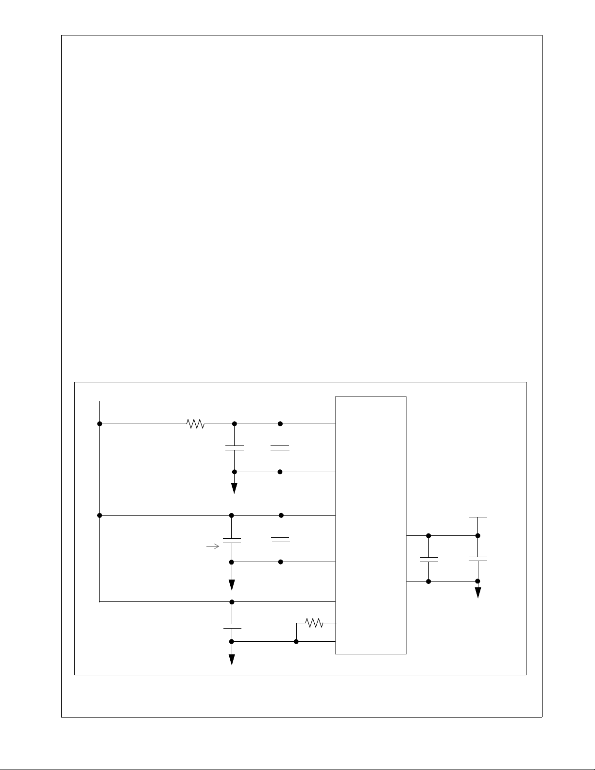
3.1 Power Supply Filterin
It is recommended that the PCB have at least one solid
ground plane, one solid 3.3 V plane, and one solid 1.8 V
plane, with no breaks in any of these planes. The interplane capacitance between the supply and ground planes
should be maximized by minimizing the distance between
these planes. Filling unused signal planes with copper and
connecting them to the proper power plane will also
increase the interplane capacitance. The inter-plane
capacitance acts like a short at high frequencies to reduce
supply plane impedance. Not all designs will be able to
incorporate the recommended suggestions because of
board cost constraints. Working designs have been done
using only 4 layers. National has a reference design built
using the EN Gig PHYTER and our GigMAC. This reference design is a PCI NIC card, using only 4 layers and
DP83861
having component pla ceme nt on onl y one s ide of the board
to reduce cost. The schematic, layout and gerber files for
this reference design are available upon request.
The 3.3 V & the 1.8 V supply pins come in pairs with their
corresponding ground pins (i.e. a 3.3 V supply-ground pair
is formed by pin 2 [RA_AVDD] and pin 3 [RA_AGND]).
These paired pins are physically adjacent to each other.
The matching pins should be bypassed with low impedance surface mo unt capacito rs of value 0.1 µF connected
directly into the p ower plan es w ith vi as as clo se as poss ible
to the pins. This will reduce the inductance in series with
the bypass ca paci t or. Any incr eas e in in d uc tan ce wil l l owe r
the capacitor’s self resonant frequency which will degrade
the high frequency performance of the capacitor. It’s also
recommended that 0.01 µF capacitors are connected in
parallel with the 0.1 µF capacitors, or at least "dispersed",
replacing some of the 0.1 µF capacitors. The lower value
capacitance will increase the frequency range of effectiveness of the bypassing scheme. This is due to the unavoidable inductance o f th e l eads and connections on the board,
which cause resonance at low frequencies for large value
capacitors.
The Analog PGM supply requires special filtering to attenuate high frequencies. High frequencies will increase the jitter of the PGM. We recommend a low pass filter formed by
a 18-22 Ω resistor and two capacitors in parallel. One of
the capacitors should be 22 µF a nd the other 0.01 µF. (This
will implem ent a single pole low pass fi lter with 3 dB f req.
around 360 - 400 Hz.). The maximum current on this supply is 5 mA.
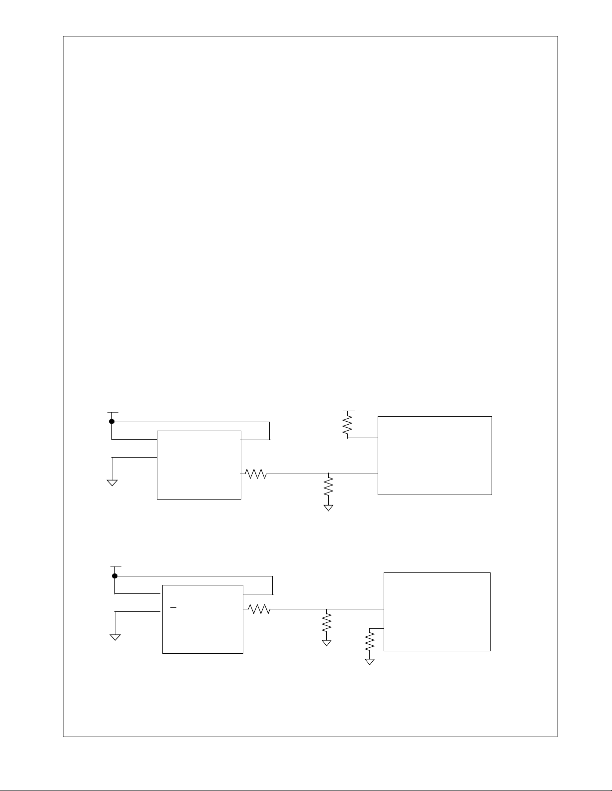
= 3.3 V
V
DD
Typical supply bypassing
(Near pins of the device)
Low pass filter for
PG M _AVDD only
18
Ω −
22
Ω
22
µF
0.01 µF
0.01
µF
0.01
0.1
µF
µF
9.31 k
DP83 861
PGM_A
PGM_AGND
IO_
VDD
CORE_
IO_GND
BG_A
Ω
BG_REF
AGND
VDD
CORE_
VDD
VDD
VSS
0.01 µF
V
DD
= 1.8 V
0.1
µF
ure 1. Power Supply Filterin
Fi
17 www.national.com
Page 18
A 10 µF capacitor should also be placed close to the
g
DP83861 (possibly on the bottom side of the PCB) bypassing the VCC and ground planes.
There has been considerable discussion in the literature
about the use of ferrite beads to isolate power plane noise
from certain noisy VCC pins and preventing this noise from
coupling into sensitive analog VCC pins. This is typically
achieved by using ferrite beads (inductors) between noisy
VCC and quiet VCC line. An inductor in conjunction with
the bypass capacitor at the VCC pins will form a low pass
filter which will prevent the high frequency noise from coupling into the quite VCC. However, using this scheme can
give mixed results. There is considerable debate about
whether this approach is necessary or even useful. In most
of our boards we put in a stuffing option for inductors (zero
Ohm resistors). In general we have not found any improvements with th e us e of ferr ite bea ds, ho we ver no ise cons iderations are very dependent on PCB’s specific layout,
function and power supplies. The board designer should
evaluate whether they w ill ben efi t from ferr ite b eads in their
particular board.
The pin check list on Table 14 show the suggested connections of these capacitors for every supply, ground and substrate pin.
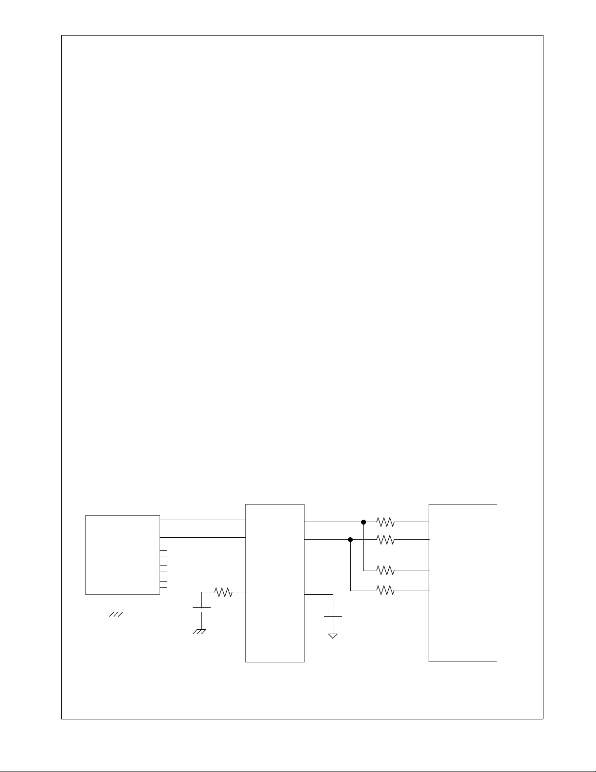
3.2 Twisted Pair Interface
The Twisted Pair Interface consists of four differential
transmit pairs (Channels A, B, C, and D) and four differen tial receive pairs (Channels A, B, C, and D). Each transmit
pair is connected to its’ corresponding receive pair through
47 Ω and 150 Ω resistors respectively (The two 47 Ω resistors in combination with the so urce imp edanc e of the transmitter will form a 100 Ω differential input impedance as
seen from the line. This is required to minimize reflections.). Figure 2 shows a typical connection for Channel A.
Channels B, C, and D are identical. The combined transmit
and receive trace then goes directly to 1:1 magnetics. We
currently recommend using the Pulse H-5007 or Pulse H-
5008. Both magnetics are pin for pin compatible, but with
different package orientations. The H-5007/8 has an isolation transformer followed by a common mode choke to
reduce EMI. There is an additional auto-transformer which
is center tapped. These 2 transformers as well as other
suppliers’ transformers from Halo, Belfuse, Transpower,
Midcom, etc. should be evaluated for best performance for
each design. See Table 9 and Table 10.
Ω
— Place the 47
1% transmit r esistors as close as possi-
ble to the TXDA+/-, TXDB+/-, TXDC+/-, and TXD+/- pins
— Place the 150
Ω 1% receive resistors close as possible
to the RXDA+/-, RXDB+/-, RXDC+/-, and RXDD+/- pins.
— All traces to and from the twisted pair interface should
have a controlled impedance of 50 Ω to the ground
plane. This is a strict requirement. They should be as
close in length to each other as possible to prevent mismatches in delay which will increase common mode
noise.
Ideally there should be no crossovers or vias on the signal
paths of these traces.
3.3 MAC Interface
The DP83861 can be configured in one of two different
modes:
— GMII (Gigabit Media Indep endent Interface) MODE : This
interfaces is used to support 802.3z compliant 1000
Mb/s MACs.
— MII (Media Independent Inte rface) MODE: This interface
is used to support 10/100 Mb/s MACs.
Only one mode can be supported at a time, since the GMII
and MII share some pins in common.
These outputs are capable of driving 35 pF under worst
case conditions. Thes e outputs were not designed to drive
multiple loads, connectors, backplanes, or cabl es. It is recommended that the outputs be series terminated through a
resistor as close to the output pins as possible. The purpose of the series termination is to reduce reflections on
the line. The value of the series termination and length of
trace the output c an driv e will de pend on the dr iver out put
impedance, the characteristic impedance of the PCB trace
(we recommend 50
(capacitance/inch), and the load capacitance (MAC input).
For short traces, less than 0.5 inches, the series resistors
may not be required, thus reducing component count.
However, each specific board design should be evaluated
for reflections and signal integrity to determine the need for
the series terminations. As a general rule of thumb, if the
trace length is less than 1/6 of the equivalent length of the
Ω
), the distributed trace capacitance
DP83861
RJ-45
1
2
3
6
4
5
7
8
A+
AB+
BC+
CD+
D-
100 pF
3 kV
75
MX4+
MX4-
Ω
MCT4
TD4+
TD4-
TCT4
0.1
µF
47
47
150
150
Ω
Ω
Ω
Ω
PULSE H-5007
DP83861
TXDA+
TXDA-
RXDA+
RXDA-
Chassis Ground
Chassis Ground
Only the connections for one of the twisted pair channels is shown. Connections for channels B, C, D are similar.
Fi
ure 2. Twisted Pair / Magnetics Interface (Channel A Only)
18 www.national.com
Page 19
rise and fall times then the series terminations might not be
g
g
g
g
needed. Equivalent length of rise time = Rise time (ps) /
Delay (ps/inch). Rise and fall times are required to be less
than 1 ns for some GMII s ignal s, typi cally being in the ord er
of 500 ps for those pins. (i.e. RX_CLK, GTX_CLK). Delay
typically = 170 ps/inch on a FR4 board. Using the above
numbers we get critical trace length = (1/6) *(500/ 170) =
0.5 inches.
.In summary:
— Place series termination resis tors as close to the pi ns as
possible.
— Keep capacitance < 35 pF as seen by the output.
— Keep output trace lengths approximately the same
length to avoid skew problems.
— Keep input trace lengths approximately the same length
to avoid skew problems.
All GMII traces should be impedance controlled. 50 ohms
to ground plane is recommended, but this is not a strict
requirement and the board designer can experiment with
different values if needed, to minimize reflections
3.4 Clocks
REF_CLK is capable of using either a 125 MHz oscillator
or a 25 MHz oscillator. The 125 MHz or 25 MHz clock is
used by the internal PLL to generate the various clocks
needed both internally and externally. This input should
come from an 125 MH z os ci lla tor (+/- 50 ppm, < 25ps cycle
to cycle jitter, < 200 ps accumulative jitter) or a 25 MHz
oscillator (+/- 50 ppm, < 25ps cycle to cycle jitter, < 200 ps
accumulative jitter). For 125 MHz operation, REF_SEL (pin
154) must be either connected directly to a 3.3 V supply or
pulled high through a 2 KΩ resistor t o a 3 .3 V supply. When
using a 25 MHz oscillator the REF_SEL (pin 154) should
be pulled to ground through a 2 KΩ resistor.
The cycle to cy cle ji tter an d the lo ng te rm accum ulati ve jitter (accumulative jitter can be measured using an osilloscope with a delay trigger set at 10 µs or using a
Wavecrest TIA). Both the 125 MHz and 25 MHz oscillators
should have less than 25 ps of cycle to cycle jitter and less
than 200 ps accumulative jitter for optimal cable performance.
Te st in
using the 25 MHz oscillator showed
that the DP83861 will exceed the 100 meter cable
th requirement in 1000 Mb/s, 100 Mb/s and 10
len
Mb/s, but the transmit jitter in 1000 mb/s mode will be
outside the IEEE spec. 40.6. 1.2 .5 (tra nsm it cl ock jitter +
transmit output jitter) of less than 300 ps.
The clock signal requires the same termination considerations mentioned in the MAC interface section. The clock
signal might require both series source termination (R
the output of the clock source and/or load termination (RT)
S
) at
close to the PHY to eliminate reflections. This will depend
on the distance of the clock source from the PHY clock
input, the source impedance of the clock source, as well as
the board impedance for the clock line considered as a
transmissio n line. Typically no ser ies or lo ad term inatio n is
required for short traces. For long traces a series resistor is
recommended. Unlike load termination, this doesn’t add to
the load current. The value of the series termination resistor has to be chosen to match the line impedance. As an
example, if the clock source has output impedance of 20Ω
and the clock tr ace has transm ission lin e impedance Zo =
50Ω then Rs = 50 - 20 = 30Ω.
DP83861
VDD = 3.3 V
GND
VDD = 3.3 V
V
DD
125 M Hz O sc
+ 50 ppm
< 2 5 p s Jitte r
(Cycle to Cycle)
< 200 ps Jitter
(Accumulative)
V
DD
25 M Hz O sc
GND
+ 50 ppm
< 2 5 p s J itter
(Cycle to Cycle)
< 200 ps Jitter
(Accumulative)
VDD = 3.3 V
DP83861
2K
Ω
ENA
Tie high
Rs
(Optional)
ure 3. 125 MHz Oscillator Option
Fi
Zo
R
(Optional)
T
REF_SEL
REF_CLK
DP83861
ENA
Rs
(Optional)
Zo
R
(Optional)
T
2K
Ω
REF_CLK
REF_SEL
ure 4. 25 MHz Oscillator Option
Fi
19 www.national.com
Page 20
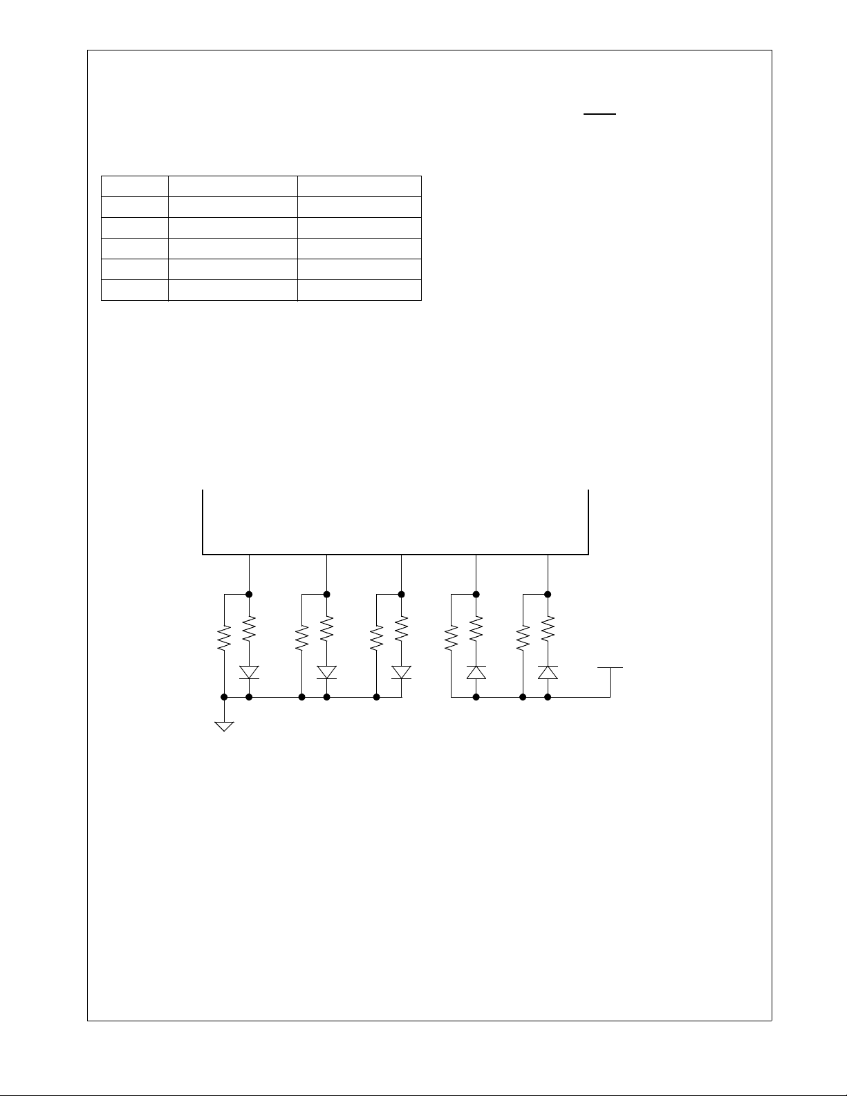
3.5 Strapping Options
g
3.5.1 PHY ADDRESS/ LED STRAPPING
The five PHY address inputs pins are shared with the LED
pins as shown below.
Table 8. PHY Address Mappin
Pin # PHYAD Function LED Function
200 PHYAD_0 ACT
201 PHYAD_1 COL
204 PHYAD_2 LNK
205 PHYAD_3 TX
207 PHYAD_4 RX
The DP83861 can be set to respond to any of 32 possible
PHY addresses. (However PHY Address = 0 will put the
EN Gig PHYTER in power-down/isolate mode. When in
power-down/isolate mode the part turns off it’s transmitter,
receiver and GMII inputs/outputs. When in this mode the
part will only respond to MDIO/MDC activity. After poweron, the PHY should be taken out of power-down isolation
by resetting bit 11 of register 0x00.) Each DP83861 or port
sharing an MDIO bus in a system must have a unique
physical address.
The pull-up or pull-down state of eac h of th e PH YAD inputs
is latched (register 0x10) at system power-up/reset. For
further de tail rel ating to the latch- in timing requi rements of
the PHY Address pins, as well as the other hardware configuration pins, refer to the Reset
Since the PH YAD strap opti on s sh ar e t he LED o utp ut pi n s,
the external components required for strapping and LED
usage must be considered in order to avoid contention.
Specifically, when the LED outputs are used to drive LEDs
directly, the active state of each output driver is dependent
on the logic level sampled by the corresponding PHYAD
input upon power-up/reset. For example, if a given PHYAD
input is resistively pu lled low then the corresponding output
will be con figur ed as a n acti ve hig h dri ver. Convers ely, if a
given PHYAD input is resistively pulled high then the corresponding output will be configured as an active low driver.
Refer to Figure 5 for an example of LED & PHYAD connection to external components. In this example, the PHYAD
strapping results in address 00011 (03h).
This adaptive nature for choosing the active high or active
low configuration applies to all the LED pins; not just the
LED pins associated wi th PHYAD strap options. So all LED
pins will be high active if th e strap value dur ing reset on
that specific LED pin was a ‘0 ’. Else if the strap va lue wa s a
‘1’ then the LED will be low active.
timing in Section 5.7.
DP83861
Ω
1 k
LED_RX
Ω
324
Figure 5. PHYAD Strapping and LED Loading Example
Ω
1 k
LED_TX
PHYAD3 = 0PHYAD4 = 0
Ω
324
LED_LNK
Ω
1 k
3.6 Unused Pins/Reserved Pins
It is well known that unused CMOS input pins should not
be left floating. This could result in inputs floating to intermediate values halfway between VCC and ground and
turning on both the NMOS and the PMOS transistors, thus
resulting in high DC currents. It could also result in oscillations. Therefore unused inputs should be tied high or low.
In theory CMOS inputs ca n be directly tied to VCC or GND.
This method has the advantage of minimizing component
count and board area. However, it’s considered safer to
pull the unused input pins high or low with a pull-up or pulldown resistor. This will prevent excessive currents in case
of a defect in the input structure, shorting either VCC or
GND to the input. Another advantage of this method is to
reduce chances of latch-up. As a compromise between the
LED_COL
Ω
Ω
324
1 k
two approaches, one can group together adjacent unused
input pins, and as a group pull them up or down using a
single resistor. See “Reference design schematics” for a
detailed example o f h ow unused pins can be grouped to be
pulled-down using a single resis tor.
Typi cal un used inpu t pins c an be th e JTAG pins TDI, TRST,
TMS and TCK which can be all tied together and pulleddown using a 2 kΩ resistor. Some of the other reserved or
unused pins include pins 186 and 206 (TEST); pins 165,
166,169,170,174,175,176, and 177 (RESERVE_GND); pin
104 (SI). All these pins except TEST pins can be pulleddown using a 2 kΩ resistor per group of pins. TEST pins
can be pulled up or tied to VCC.
Ω
324
Ω
1 k
LED_ACT
PHYAD0 = 1PHYAD1 = 1PHYAD2 = 0
Ω
324
VDD = 3.3 V
20 www.national.com
Page 21
In general, using pull-up and pull-down resistors instead of
g
tying unused inputs directly to VCC or ground has the following disadvantages:
— Additional cost of components
— Additional board area. (May preve nt fitting into few er lay-
ers of PCB, having components only on the top side, or
fitting into small profile cards.)
— Reliability problems (Due to bad solder joints, etc.)
— Need to test components: Might necessitate additional
vias to be drilled to have test points on th e back si de, for
in circuit test. This adds to PCB ma nufacturing tim e, and
cost. Also testing additi onal compone nts add to in circ uit
test duration, and makes the test program longer to
write.
— Inventory costs for the additional components
3.7 Hardware Reset
RESET pin 164 which is acti ve low shou ld be held low for a
minimum of 140 µs to allow hardware reset. During hardware reset the strap optio n pins are re-l atche d, and reg ister
and state machines are reset. For timing details see
Figure 5.7. There is no on-chip internal power-on reset and
the DP83861 requires an external reset signal be applied
to the RESET
pin.
3.8 Temperature Considerations
The DP83861 utilizes an enhanced 208 PQFP package
that eliminates the need for heatsinks. The package has a
built in copper heat slug at the top of the package which
provides a very efficient method of removing heat from the
die through convection. Since the heat slug is on the top of
the package the PCB board stays cooler. The enhance
package has a low Theta Junction to Case of 2.13
and a Theta Junction to Ambient of 11.7 oC/W.
For reliability purpos es the die tempera ture of t he DP8 3861
should be kept below 120
case temperature of 112
this calculation is do ne see Sec tion 8.15 (Frequently Aske d
Questions)
o
C, this translates to a package
o
C. For more information on how
o
C/W
3.9 Pin List and Connections
Table 14 provides pin listings and their connections. This
list should be used to make sure all pin connec tions are
correct.
DP83861
Table 9. Ma
Parameter Min. Typ. Max. Units Conditions
Turns Ratio - 1:1 - - +/- 2%
Insertion Loss 0.0 - 1.1 dB 0.1 - 1 MHz
Return Loss -18 - - dB 1.0 - 30 MHz
-14.4 - - dB 30 - 40 MHz
-13.1 - - dB 40 - 50 MHz
-12.0 - - dB 50 - 80 MHz
-10.0 - - dB 80 - 100 MHz
Differential to Common Mode Rejection -43.0 - - dB 1.0 - 30 MHz
-37.0 - - dB 30 - 60 MHz
-33.0 - - dB 60 - 100 MHz
Cross Talk -45.0 - - dB 1.0 - 30 MHz
-40.0 - - dB 30 - 60 MHz
-35.0 - - dB 60 - 100 MHz
Isolation 1500 - - V Rise Time - 1.6 1.8 ns 10 - 90%
Primary Inductance 350 - - µH-
netic Requirements
- - 0.5 dB 1.0 - 60 MHz
- - 1.0 dB 60 - 100 MHz
- - 1.2 dB 100 - 125 MHz
21 www.national.com
Page 22
Table 10. Magnetic Manufacturers
Manufacture Website Part Number
Pulse Engineering www.pulseeng.co m H5007
H5008
Bel Fuse www.belfuse.com S558-5999-P3
Delta www.delta.tw LF9203
Halo www.haloelectronics.com TG1G-S002NZ
Midcom www.midcom-inc.com 000-7044-37R
Transpower www.trans-power.com GB1G01
Contact Magnetics manufactures for latest part numbers and product specifica-
Note:
tions. All Magnet ics s hould be thoroug hly te sted and v alida ted be fore u sing them in pro duction.
Table 11. 25 MHz Oscillator Requirements
Parameter Min. Typ. Max. Units Conditions
Frequency - 25 - MHz Frequency Stability - 50 0 50 ppm
Rise/Fall Time ns 20 - 80%
Symmetry 40 60 % duty cycle
Jitter (Cycle to Cycle) - 25 ps rising edge to rising edge
Jitter (Accumulative) 200 ps delay trigger 10 µs
Logic 0 10% VDD V VDD = 2.5 or 3.3 V nominal
Logic 1 90% Vdd V VDD = 2.5 or 3.3 V nominal
S558-599-T3
000-7093-37R
GB1G04
0 to 70
o
C
DP83861
Table 12. 125 MHz Oscillator Requirements
Parameter Min. Typ. Max. Units Conditions
Frequency - 125 - MHz Frequency Stability - 50 0 50 ppm
Rise/Fall Time 2.5 ns 20 - 80%
Symmetry 40 60 % duty cycle
Jitter (Cycle to Cycle) - 25 ps rising edge to rising edge
Jitter (Accumulative) 200 ps delay trigger 10 µs
Logic 0 10% VDD V VDD = 2.5 or 3.3 V nominal
Logic 1 90% Vdd V VDD = 2.5 or 3.3 V nominal
0 to 70
o
C
22 www.national.com
Page 23

Table 13. Oscillator Manufacturers
Manufacture Website Part Number
Vite Technology www.viteonline.com 25 MHz (VCC1-B2B-25M000)
125 MHz (VCC1-B2B-125M000)
SaRonix www.saronix.com 125 MHz (SCS-NS-1132)
Valpey Fisher www.valpeyfisher.com 125 MHz (VAC570BL)
Contact Oscilla tor m an ufac tures for latest information on part numbers and product
Note:
specifications. All O scil lators shoul d be th oroughl y tes ted and valid ate d befor e usin g them
in production.
125 MHz (VFAC38L)
DP83861
23 www.national.com
Page 24

Table 14. Pin List
g
g
g
g
g
g
g
g
g
g
Pin # DataSheet Pin Name Type Connections/
Comments
DP83861
1 RA_ASUB Ground
2 RA_AV
DD
Power
3 RA_AGND Ground
4 RXDA+ Input
5 RXDA- Input
6 RA_AV
DD
Power
7 RA_AGND Ground
8 CDA_AV
DD
Power
9 TXDA+ Output
10 TXDA- Output
Substrate Ground
Receive Analog 3.3 V Supply
: Connect to ground plane.
: Bypass to pin 3 using
a 0.1 µF capacitor.
Receive Analo
Ground
Channel A Receive Data Positive
: Connect to ground plane.
: Connect to pin 12
of the H-5007 magnetics thr ough a 150 Ω, 1% resistor.
See Figure 2
: Connect to p in 11
Channel A Receive Data Ne
ative
of the H-5007 magnetics thr ough a 150 Ω, 1% resistor.
See Figure 2.
Receive Analog 3.3V Supply
: Bypass to pin 7 using a
0.1 µF capacitor.
Receive Analo
Ground
Transmit Analog 3.3V Supply
: Connect to ground plane.
: Bypass to pin 11 usi ng
a 0.1 µF capacitor.
Channel A Transmit Data Positive
: Connect to pin 12
of the H-5007 magnetics through a 47 Ω, 1% resist or.
See Figure 2.
: Connect to pin
Channel A Transmit Data Ne
ative
11 of the H-5007 magnetics through a 47 Ω, 1% resis-
tor. See Figure 2.
11 CDA_AGND Ground
12 CDB_AGND Ground
13 TXDB- Output
14 TXDB+ Output
15 CDB_AV
DD
Power
16 RB_AGND Ground
17 RB_AV
DD
Power
18 RXDB- Input
19 RXDB+ Input
20 RB_AGND Ground
21 RB_AV
DD
Power
Transmit Analo
Transmit Analo
Ground
Ground
Channel B Transmit Data Ne
: Connect to ground plane.
: Connect to ground plane.
: Connect to pin 9
ative
of the H-5007 magnetics through a 47 Ω, 1% resistor.
See See Figure 2.
Channel B Transmit Data Positive
: Connect to pin 8
of the H-5007 magnetics through a 47 Ω, 1% resistor.
See See Figure 2.
Transmit Analog 3.3V Supply
: Bypass to pin 12 usi ng
a 0.1 µF capacitor.
Receive Analo
Ground
Receive Analog 3.3V Supply
: Connect to ground plane.
: Bypass to pin 16 using
a 0.1 µF capacitor.
: Connect to pin 9
Channel B Receive Data Ne
ative
of the H-5007 magnetics thro ugh a 150 Ω, 1% resistor.
See Figure 2.
Channel B Receive Data Posi tive
: Connect to pin 8 of
the H-5007 magnetics through a 150 Ω, 1% resistor.
See Figure 2.
Receive Analo
Ground
Receive Analog 3.3V Supply
: Connect to ground plane.
: Bypass to pin 20 using
a 0.1 µF capacitor.
24 www.national.com
Page 25

g
g
g g
g
g
g
g
g
g
Pin # DataSheet Pin Name Type Connections/
Comments
DP83861
22 RB_ASUB Ground
23 BG_AV
DD
Power
24 BG_REF Input
25 BG_AGND Ground
26 BG_SUB Ground
27 PGM_AV
DD
Power
28 PGM_AGND Ground
29 SHR_V
DD
Power
30 SHR_GND Ground
31 RC_ASUB Ground
32 RC_AV
DD
Power
33 RC_AGND Ground
Substrate Ground
Bandgap 3.3V Supply
: Connect to ground plane.
: Connect to pin 25 using a 0.01
µF capacitor.
Band
ap Reference
: Connect to pin 25 using a 9.31 K
Ω, 1% resistor. The resistor shou ld b e pla ce d as close
to pin 24 as possible to r educe trace ind uctance and reduce the possibility of picking up noise through
crosstalk.
ap Ground
Band
Bandgap Substrate
PGM Analog 3.3V Supply
PGM Ground
Analog 3.3V Supply
: Connect to ground plane.
: Connect to ground plane.
: See Figure 1
: Connect to ground plane.
: Connect to pin 30 using a 0.1 µF
capacitor.
: Connect to ground plane.
Analo
Substrate Ground
Receive Analog 3.3V Supply
round
: Connect to ground plane.
: Bypass to pin 33 using
a 0.1 µF capacitor.
Receive Analo
Ground
: Connect to ground plane.
34 RXDC+ Input
35 RXDC- Input
36 RC_AV
DD
Power
37 RC_AGND Ground
38 CDC_AV
DD
Power
39 TXDC+ Output
40 TXDC- Output
41 CDC_AGND Ground
42 CDD_AGND Ground
43 TXDD- Output
Channel C Receive Data Posi tive
: Connect to pin 6 of
the H-5007 magnetics through a 150 Ω resistor (1%).
See Figure 2.
: Connect to pin 5
Channel C Receive Data Ne
ative
of the H-5007 magnetics through a 150 Ω resisto r (1%).
See Figure 2.
Receive Analog 3.3V Supply
: Bypass to pin 37 using
a 0.1 µF capacitor.
Receive Analo
Ground
Transmit Analog 3.3V Supply
: Connect to ground plane.
: Bypass to pin 41 usi ng
a 0.1 µF capacitor.
Channel C Transmit Data Positive
: Connect to pin 6
of the H-5007 magnetics through a 47 Ω, 1% resistor.
See Figure 2.
Connect to pin 5
Channel C Transmit Data Ne
ative
of the H-5007 magnetics through a 47 Ω resistor (1%).
See Figure 2.
Transmit Analo
Ground
Transmit Analog Ground
Channel D Transmit Data Ne
: Connect to ground plane.
: Connect to ground plane.
: Connect to pin 3
ative
of the H-5007 magnetics through a 47 Ω resistor (1%).
See Figure 2.
25 www.national.com
Page 26

g
g
g
g
g
Pin # DataSheet Pin Name Type Connections/
Comments
DP83861
44 TXDD+ Output
45 CDD_AV
DD
Power
46 RD_AGND Ground
47 RD_AV
DD
Power
48 RXDD- Input
49 RXDD+ Input
50 RD_AGND Ground
51 RD_AV
DD
Power
52 RD_ASUB Ground
53 RESERVE_FLOAT
54 RESERVE_FLOAT
Channel D Transmit Data Positive
: Connect to pin 2
of the H-5007 magnetics through a 47 Ω, 1% resistor.
See Figure 2.
Transmit Analog 3.3V Supply
: Bypass to pin 42 usi ng
a 0.1 µF capacitor.
Receive Analo
Ground
Receive Analog 3.3V Supply
: Connect to ground plane.
: Bypass to pin 46 using
a 0.1 µF capacitor.
: Connect to pin 3
Channel D Receive Data Ne
ative
of the H-5007 magnetics through a 150 Ω resisto r (1%).
See Figure 2.
Channel D Receive Data Posi tive
: Connect to pin 2 of
the H-5007 magnetics through a 150 Ω resistor (1%).
See Figure 2.
Receive Analo
Ground
Receive Analog 3.3V Supply
: Connect to ground plane.
: Bypass to pin 50 using
a 0.1 µF capacitor.
Substrate Ground
Reserved
Reserved
: Leave floating.
: Leave floating.
: Connect to ground plane.
55 RESERVE_FLOAT
56 RESERVE_FLOAT
57 IO_VSS Ground
58 IO_V
DD
Power
59 RESERVE_FLOAT
60 RESERVE_FLOAT
61 RESERVE_FLOAT
62 RESERVE_FLOAT
63 IO_VSS Ground
64 IO_V
DD
Power
65 RESERVE_FLOAT
66 RESERVE_FLOAT
67 CORE_SUB Ground
68 CORE_VSS Ground
69 CORE_V
DD
Power
Reserved
Reserved
I/O Ground
I/O 3.3V Supply
: Leave floating.
: Leave floating.
: Connect to ground plane.
: Bypass to pin 57 using a 0.1 µF ca-
pacitor.
Reserved
Reserved
Reserved
Reserved
I/O Ground
I/O 3.3V Supply
: Leave floating.
: Leave floating.
: Leave floating.
: Leave floating.
: Connect to ground plane.
: Bypass to pin 63 using a 0.1 µF ca-
pacitor.
Reserved
Reserved
Di
Di
: Leave floating.
: Leave floating.
ital Core Substrate
ital Core Ground
: Connect to ground plane.
: Connect to ground plane.
Digital Core 1.8 V Supply
0.1 µF capacitor.
: Bypass to pin 68 using a
70 RESERVED_FLOAT
Reserved
: Leave floating.
26 www.national.com
Page 27

g
g
g
Pin # DataSheet Pin Name Type Connections/
Comments
DP83861
71 RESERVED_FLOAT
72 IO_VSS Ground
73 IO_V
DD
Power
74 RESERVE_FLOAT
75 RESERVE_FLOAT
76 RESERVE_FLOAT
77 RESERVE_FLOAT
78 IO_VSS Ground
79 IO_V
DD
Power
80 RESERVE_FLOAT
81 RESERVE_FLOAT
82 CORE_VSS Ground
83 CORE_V
DD
Power
84 RESERVE_FLOAT
Reserved
I/O Ground
I/O 3.3V Supply
: Leave floating.
: Connect to ground plane.
: Bypass to pin 72 using a 0.1 µF ca-
pacitor.
Reserved
Reserved
Reserved
Reserved
I/O Ground
I/O 3.3V Supply
: Leave floating.
: Leave floating.
: Leave floating.
: Leave floating.
: Connect to ground plane.
: Bypass to pin 78 using a 0.1 µF ca-
pacitor.
Reserved
Reserved
Di
: Leave floating.
: Leave floating.
ital Core Ground
: Connect to ground plane.
Digital Core1.8 V Supply
µF capacitor.
Reserved
: Leave floating.
: Bypass to pin 82 using a 0.1
85 RESERVE_FLOAT
86 IO_VSS Ground
87 IO_V
DD
Power
88 RESERVE_FLOAT
89 RESERVE_FLOAT
90 RESERVE_FLOAT
91 RESERVE_FLOAT
92 IO_VSS Ground
93 IO_V
DD
Power
94 RESERVE_FLOAT
95 RESERVE_FLOAT
96 CORE_SUB Ground
97 CORE_VSS Ground
98 CORE_V
DD
Power
Reserved
I/O Ground
I/O 3.3V Supply
: Leave floating.
: Connect to ground plane.
: Bypass to pin 86 using a 0.1 µF ca-
pacitor.
Reserved
Reserved
Reserved
Reserved
I/O Ground
I/O 3.3V Supply
: Leave floating.
: Leave floating.
: Leave floating.
: Leave floating.
: Connect to ground plane.
: Bypass to pin 92 using a 0.1 µF ca-
pacitor.
Reserved
Reserved
Di
Di
: Leave floating.
: Leave floating.
ital Core Substrate
ital Core Ground
: Connect to ground plane.
: Connect to ground plane.
Digital Core 1.8 V Supply
0.1 µF capacitor.
: Bypass to pin 97 using a
99 RESERVE_FLOAT
100 RESERVE_FLOAT
Reserved
Reserved
: Leave floating.
: Leave floating.
27 www.national.com
Page 28

Pin # DataSheet Pin Name Type Connections/
Comments
DP83861
101 IO_VSS Ground
102 IO_V
DD
Power
103 RESERVE_FLOAT
104 SI
105 SO
106 RESERVE_FLOAT
107 RESERVE_FLOAT
108 IO_VSS Ground
109 IO_V
DD
Power
110 COL Output
111 CRS Output
I/O Ground
I/O 3.3V Supply
: Connect to ground plane.
: Bypass to pin 101 using a 0.1 µF ca-
pacitor.
Reserved
: Leave floating.
SI
SO
Reserved
Reserved
I/O Ground
I/O 3.3V Supply
: Leave floating.
: Leave floating.
: Leave floating.
: Leave floating.
: Connect to ground plane.
: Bypass to pin 108 using a 0.1 µF ca-
pacitor.
Collision
: Connect to MAC c hi p through a single 50 Ω
impedance trace. This output is capable of driving 35
pF load and is not in tended to drive conne ctors, cable s,
backplanes or m ultiple t races. Thi s appli es if the part is
in 100 Mb/s mode or 1000 Mb/s mode.
Carrier Sense
: Connect to MAC chip through a single
50Ω impeda nce trace. Thi s output is cap able of drivin g
35 pf load and is not intended to drive connectors, cables, backplanes or multiple traces. This applies if the
part is in 100 Mb/s mode or 1000 Mb/s mode.
112 RX_ER Output
113 RX_DV Output
114 RXD7 Output
115 RXD6 Output
116 IO_VSS Ground
117 IO_V
DD
Power
Receive Error/Receive Data 9
: Connect to MAC chip
through a single 50 Ω impedance trace. This output is
capable of driving 3 5 pf load and is not int ended to drive
connectors, cables , backplanes or multi ple traces. This
applies if the part is in 100 Mb/s mode or 1000 Mb/s
mode.
Receive Data Valid/Receive Data 8
: Connect to MAC
chip through a single 50 Ω impedance trace. This output is capable of driving 35 pf load and is not intended
to drive connectors, cables, backplanes or multiple
traces. This applies if the part is in 100 Mb/s mode or
1000 Mb/s mode.
Receive Data 7:
Connect to MAC chip thro ugh a single
50 Ω impedance trace. T his outp ut is capabl e of driv ing
35 pf load and is not intended to drive connectors, cables, backplanes or multiple traces. This applies if the
part is in 100 Mb/s mode or 1000 Mb/s mode.
Receive Data 6:
Connect to MAC chip thro ugh a single
50 Ω impedance trace. T his outp ut is capabl e of driv ing
35 pf load and is not intended to drive connectors, cables, backplanes or multiple traces. This applies if the
part is in 100 Mb/s mode or 1000 Mb/s mode.
I/O Ground
I/O 3.3V Supply
: Connect to ground plane.
: Bypass to pin 116 using a 0.1 µF ca-
pacitor.
28 www.national.com
Page 29

g
g
Pin # DataSheet Pin Name Type Connections/
Comments
DP83861
118 RXD5 Output
119 RXD4 Output
120 RXD3 Output
121 RXD2 Output
122 IO_VSS Ground
123 IO_V
DD
Power
124 RXD1 Output
Receive Data 5:
Connect to MAC chip thro ugh a single
50 Ω impedance trace. T his outp ut is capabl e of driv ing
35 pf load and is not intended to drive connectors, cables, backplanes or multiple traces. This applies if the
part is in 100 Mb/s mode or 1000 Mb/s mode.
Receive Data 4:
Connect to MAC chip thro ugh a single
50 Ω impedance trace. T his outp ut is capabl e of driv ing
35 pf load and is not intended to drive connectors, cables, backplanes or multiple traces. This applies if the
part is in 100 Mb/s mode or 1000 Mb/s mode.
Receive Data 3:
Connect to MAC chip thro ugh a single
50 Ω impedance trace. T his outp ut is capabl e of driv ing
35 pf load and is not intended to drive connectors, cables, backplanes or multiple traces. This applies if the
part is in 100 Mb/s mode or 1000 Mb/s mode.
Receive Data 2:
Connect to MAC chip thro ugh a single
50 Ω impedance trace. T his outp ut is capabl e of driv ing
35 pf load and is not intended to drive connectors, cables, backplanes or multiple traces. This applies if the
part is in 100 Mb/s mode or 1000 Mb/s mode.
I/O Ground
I/O 3.3V Supply
: Connect to ground plane.
: Bypass to pin 122 using a 0.1 µF ca-
pacitor.
Receive Data 1:
Connect to MAC chip thro ugh a single
50 Ω impedance trace. T his outp ut is capabl e of driv ing
35 pf load and is not intended to drive connectors, cables, backplanes or multiple traces. This applies if the
part is in 100 Mb/s mode or 1000 Mb/s mode.
125 RXD0 Output
126 RX_CLK Output
127 CORE_SUB Ground
128 CORE_VSS Ground
129 CORE_V
DD
Power
130 TX_CLK Output
131 IO_VSS Ground
132 IO_V
DD
Power
Receive Data 0:
Connect to MAC chip thro ugh a single
50 Ω impedance trace. T his outp ut is capabl e of driv ing
35 pf load and is not intended to drive connectors, cables, backplanes or multiple traces. This applies if the
part is in 100 Mb/s mode or 1000 Mb/s mode.
Receive Clock/ Receive Byte Clock 1
: Connect to
MAC chip through a single 50 Ω impedance trace. Thi s
output is capable of driv ing 35 pf load and is not inte nded to drive connectors, cables, backplanes or multiple
traces. This applies if the part is in 100 Mb/s mode or
1000 Mb/s mode.
ital Core Substrate
Di
ital Core Ground
Di
Digital Core 1.8 V Supply
: Connect to ground plane.
: Connect to ground plane.
: Bypass to pin 128 using a
0.1 µF capacitor.
Transmit Clock/Receive Byte Clock 0
: Connect to
MAC chip through a single 50 Ω impedance trace. Thi s
input has a typical input capacitance of 6 pF.
I/O Ground
I/O 3.3V Supply
: Connect to ground plane.
: Bypass to pin 131 using a 0.1 µF ca-
pacitor.
29 www.national.com
Page 30

g
g
g
Pin # DataSheet Pin Name Type Connections/
Comments
DP83861
133 TX_ER Input
134 TX_EN Input
135 TXD7 Input
136 CORE_VSS Ground
137 CORE_V
DD
Power
138 TXD6 Input
139 TXD5 Input
140 TXD4 Input
141 TXD3 Input
Transmit Error/Transmit Data 9
: Connect to MAC
chip through a single 50 Ω impedance trace. This input
has a typical input capacitance of 6 pF.
Transmit Enable/Transmit Data 9
: Connect to MAC
chip through a single 50 Ω impedance trace. This input
has a typical input capacitance of 6 pF.
Transmit Data 7
: Connect to MAC chip through a single 50 Ω impedance trac e. This input h as a typical input
capacitance of 6 pF.
ital Core Ground
Di
Digital Core 1.8 V Supply
: Connect to ground plane.
: Bypass to pin 136 using a
0.1 µF capacitor.
Transmit Data 6
: Connect to MAC chip through a single 50 Ω impedance trac e. This input h as a typical input
capacitance of 6 pF
Transmit Data 5
: Connect to MAC chip through a single 50 Ω impedance trac e. This input h as a typical input
capacitance of 6 pF
Transmit Data 4
: Connect to MAC chip through a single 50 Ω impedance trac e. This input h as a typical input
capacitance of 6 pF
Transmit Data 3
: Connect to MAC chip through a single 50 Ω impedance trac e. This input h as a typical input
capacitance of 6 pF
142 IO_VSS Ground
143 IO_V
DD
Power
144 TXD2 Input
145 TXD1 Input
146 TXD0 Input
147 GTX_CLK Input
148 IO_VSS Ground
149 IO_V
DD
Power
150 MDIO I/O
151 MDC Input
I/O Ground
I/O 3.3V Supply
: Connect to ground plane.
: Bypass to pin 142 using a 0.1 µF ca-
pacitor.
Transmit Data 2
: Connect to MAC chip through a single 50 Ω impedance trac e. This input h as a typical input
capacitance of 6 pF
Transmit Data 1
: Connect to MAC chip through a single 50 Ω impedance trac e. This input h as a typical input
capacitance of 6 pF
Transmit Data 0
: Connect to MAC chip through a single 50 Ω impedance trac e. This input h as a typical input
capacitance of 6 pF
GMII Transmit Clock
: Connect to MAC chip through a
single 50 Ω impedanc e trace. This i nput has a typ ical input capacitance of 6 pF
I/O Ground
I/O 3.3V Supply
: Connect to ground plane.
: Bypass to pin 148 using a 0.1 µF ca-
pacitor.
Mana
ement Data I/O
: Pull-up to VCC with a 1.54 kΩ
resistor.
ement Data Clock
Mana
: Connect to MAC or cont rol-
ler using a 50 Ω impedance trace.
30 www.national.com
Page 31

g
g
g
Pin # DataSheet Pin Name Type Connections/
Comments
DP83861
152 OSC_VSS Ground
153 REF_CLK Input
154 REF_SEL Input
155 OSC_V
156 TRST
DD
Power
Input
157 TDI Input
158 TDO Output
159 TMS Input
160 CORE_V
DD
Power
161 CORE_VSS Ground
162 CORE_SUB Ground
163 TCK Input
Oscillator Ground
Reference Clock
: Connect to ground plane.
: Connect to oscillator or crystal or
board clock.
Reference Select
: Pulled high to 3.3 V supp ly th rough
a 2 KΩ resistor or tied directly to a 3.3 V supply for
125 MHz operation. Pull low for 25 MHz operation.
Oscillator 3.3V Supply
: Bypass to pin 152 u sing a 0.1
µF capacitor.
JTAG Test Reset
JTAG Test Data Input:
: If not used conne ct to groun d plane.
If not used connect to ground
plane.
JTAG Test Data Output
JTAG Test Mode Selec t:
: If not used leave floating.
If not used connect to ground
plane.
Digital Core 1.8 V Supply
: Bypass to pin 161 using a
0.1 µF capacitor.
ital Core Ground
Di
ital Core Substrate
Di
JTAG Test Clock
: Connect to ground plane.
: Connect to ground plane.
: If not used conne ct to groun d plane.
164 RESET
Input
165 RESERVE_GND
166 RESERVE_GND
167 IO_V
DD
Power
168 IO_VSS Ground
169 RESERVE_GND
170 RESERVE_GND
171 CORE_V
DD
Power
172 CORE_VSS Ground
173 CORE_SUB Ground
174 RESERVE_GND
175 RESERVE_GND
176 RESERVE_GND
177 RESERVE_GND
178 IO_V
DD
Power
: Connect to board reset signal.
Reset
Reserved
Reserved
I/O 3.3V Supply
: Pull-down to ground plane.
: Pull-down to ground plane.
: Bypass to pin 168 using a 0.1 µF ca-
pacitor.
I/O Ground
Reserved
Reserved
: Connect to ground plane.
: Pull-down to ground plane.
: Pull-down to ground plane.
Digital Core 1.8 V Supply
0.1 µF capacitor.
ital Core Ground
Di
Digital Core Substrate
Reserved
Reserved
Reserved
Reserved
: Pull-down to ground plane.
: Pull-down to ground plane.
: Pull-down to ground plane.
: Pull-down to ground plane.
I/O 3.3V Supply
: Connect to ground plane.
: Connect to ground plane.
: Bypass to pin 179 using a 0.1 µF ca-
pacitor.
: Bypass to pin 172 using a
179 IO_VSS Ground
I/O Ground
: Connect to ground plane.
31 www.national.com
Page 32

g
g
g
g
g
g
Pin # DataSheet Pin Name Type Connections/
Comments
DP83861
180 LED_10/10_ADV/SP
I/O, Strap
EED [1]
181 LED_100/100_ADV I/O, Strap
182 CORE_V
DD
Power
183 CORE_VSS Ground
184 LED_1000/
I/O, Strap
1000FDX_ADV
185 LED_DUPLEX/
I/O, Strap
1000HDX_ADV
186 TEST
187 IO_V
DD
Power
188 IO_VSS Ground
189 SDA I/O
190 SCL I /O
LED_10:
LED_100
Digital Core 1.8 V Supply
See Figure 5 for how to connect this pin.
: See Figure 5 for how to connect this pin.
: Bypass to pin 183 using a
0.1 µF capacitor.
ital Core Ground
Di
LED_1000:
See Figure 5 for how to connect t his pin. (I f
: Connect to ground plane.
this pin is strapped low, then pin 192 should be
strapped high.)
LED_DUPLEX
: See Figure 5 for how to connect this
pin.
Special pin:
I/O 3.3V Supply
Pull-up to VCC.
: Bypass to pin 188 using a 0.1 µF ca-
pacitor.
I/O Ground
SDA
terface is not used. Else see E
SCL
terface is not used. Else see E
: Connect to ground plane.
: This pin should be left floating if the E
2
PROM Usage Guide.
: This pin should be left floating if the E
2
PROM Usage Guide
2
PROM in-
2
PROM in-
191 Manual M/S Advertise I/O, Strap
192 AN_EN/TX_TCLK I/O, Strap
193 IO_V
DD
Power
194 IO_VSS Ground
195 Manual_M/S_Enable I, Strap
196 NC_MODE I/O, Strap
197 CORE_V
DD
Power
198 CORE_VSS Ground
199 CORE_SUB Ground
200 LED_ACT/PHYAD_0 I/O, Strap
201 LED_COL/PHYAD_1 I/O, Strap
Manual Master/Slave Confi
uration
: 2 kΩ pull-up or
pull-down strap option.
Auto-Ne
otiation Enable
: 2 kΩ pull-up or pull-down
strap option. (If this pin is strapped low, then pin 184
should be strapped high.)
I/O 3.3V Supply
: Bypass to pin 194 using a 0.1 µF ca-
pacitor.
I/O Ground
Manual Master/Slave Confi
: Connect to ground plane.
Enable
: 2 kΩ pull-up or
pull-down strap option.
Non Compliant Mode
: Pull high to inter-operate with
non-IEEE compliant transceivers.
Digital Core 1.8 V Supply
: Bypass to pin 198 using a
0.1 µF capacitor.
ital Core Ground
Di
ital Core Substrate
Di
Activity LED/Phy Address 0
: Connect to ground plane.
: Connect to ground plane.
: See Figure 5 for how to
connect this pin.
Collision LED/Phy Address 1
: See Figure 5 for how to
connect this pin.
202 IO_V
DD
Power
I/O 3.3V Supply
pacitor.
: Bypass to pin 203 using a 0.1 µF ca-
32 www.national.com
Page 33

Pin # DataSheet Pin Name Type Connections/
Comments
DP83861
203 IO_VSS Ground
204 LED_LNK/PHYAD_2 I/O, Strap
205 LED_TX/PHYAD_3 I/O, Strap
206 TEST
207 LED_RX/PHYAD_4 I/O, Strap
208 SPEED
[0]/PORT_TYPE
I/O, Strap
I/O Ground
Link LED/Phy Address 2
nect this pin.
Transmit LED/Phy Addr ess 3
connect this pin.
Special pin:
Receive LED/Phy Add ress 4
connect this pin.
Speed Select [0] / Port Type
strap option.
: Connect to ground plane.
: See Figure 5 on how to con-
Pull-up to VCC
: See Figure 5 on how to
: See Figure 5 on how to
: 2 kΩ pull-up or pull-down
33 www.national.com
Page 34

4.0 Functional Description
g
The DP83861 is a full feature d 10/10 0/1000 Ethernet Physical layer chip consisting of digital 10/100/1000 Mb/s core
which is integrated into a single device with a common TP
interface, combined MII/GMII controller interface and Management. interface.
COMBINED GMII, MII INTERFACE
MUX/DMUX
DP83861
4.1 1000BASE-T Functional Description
The 1000BASE-T transceiver consisting of a PCS Transmitter, PMA Transmitter, PMA Receiver and a PCS
Receiver are shown below (Figure 6) in functional block
diagram form.
MII (10/100 Mb/s)
MII
1000BASE-T
AN
1000BASE-T
SUBSYSTEM
RECEIVERS
GMII
PCS
BN
CN
PMA
DAC
DRIVERS/
TX BLOCK
ENCODE
AN,BN,CN,DN
DN
PAM-5
17 LEVEL PR SHAPED
RX BLOCK
Echo cancellation
Crosstalk cancellation
ADC
Decode/Descramble
Equalization
Timing
Skew compensation
BLW
MAGNETICS
4-PAIR CAT-5 CABLE
ure 6. 1000BASE-T Functional Block Diagram
Fi
34 www.national.com
Page 35

4.2 1000BASE-T PCS TX
g
g
g
g
The PCS transmitter consists of several functional blocks
that convert the 8-bit TXDn data from the GMII to PAM-5
symbols to be passed onto the PMA (Physical Medium
Attachment) function. The block diagram of the PCS transmitter data path fu nct ion s in Figure 7, provides an overview
of each of the functional blocks within the PCS transmitter.
The transmitter consists of eight functional blocks:
— LFSR (Linear Feedback Shift Register)
— Data scrambler and symbol sign scrambler word gener-
ator
— Scrambler bit generator
— Data scrambler
— Convolutional encoder
— Bit-to-symbol quinary symbol mapping
— Sign scrambler nibble generator
— Symbol sign scrambler
The requirements for the PCS transmit functionality are
also defined in the IEEE 802.3ab specification section
40.3.1.3 “PCS Transmit function”.
4.2.1 Linear Feedback Shift Re
The side-stream scrambler function uses a LFSR implementing one of 2 equations, based on the mode of operation being either a master or a slave. For master operation,
the equati on is as follows:
(x) = 1 + x13 + x
g
M
33
For slave operation, use the equation:
gS(x) = 1 + x20 + x
33
The 33-bit data output, Scrn[32:0], of this block is then fed
into the da ta scrambler and symb ol sign scrambler w ord
generator.
4.2.2 Data and Symbol Si
The word generator uses the Scrn[32:0] to generate further
scrambled values. The following signals are generated:
[3:0], Syn[3:0], and Sgn[3:0].
Sx
n
The 4-bit Sx
scrambler bit generator. The 4-bit Sgn[3:0] sign values are
[3:0] and Syn[3:0] values are then fed into the
n
fed into the sign scrambler nibble generator.
ister (LFSR)
n Scrambler Word Generator
4.2.3 Scrambler Bit Generator
This function uses the Sx
tx_mode and tx_enable signals to generate the Sc
which is further scrambled based on the condition of the
and Syn signals along with the
n
[7:0],
n
tx_mode and tx_enable signal. The tx_mode signal can
indicate sending idles (SEND_I), sending zeros (SEND_Z)
or sending idles/data (SEND_N). The tx_mode signal is
generated by the micro controller function. The tx_enable
signal is either asserted to indicate data transmission is
occurring or not asserted for no data transmission. The
PCS Data Transmission Enable state machine generates
the tx_enable signal.
The 8-bit Sc
bler functional block.
[7:0] signals are then fed into the data scram-
n
4.2.4 Data Scrambler
This function generates scrambled data by accepting the
[7:0] data from the GMII and scrambling it based on
TxD
n
various inputs.
The data scrambler generates the 8-bit Sd
which scram bl e s th e T xD
values and the accompanying control signals.
data based primarily on the Sc
n
[7:0] value,
n
All 8-bits of Sdn[7:0] are passed into the bit-to-quinary symbol mapping block, while 2-bits, Sd
convolutional encoder.
[7:6], are fed into the
n
4.2.5 Convolutional Encoder
The encoder uses Sd
an additional data bit, which is called Sdn[8].
The one clock d elayed vers ions cs
the data scrambler functional block. This Sdn[8] bit is then
[7:6] bits and tx_enable to generate
n
[1:0] are passed into
n-1
passed into the bit-to-symbol quinary symbol mapping
function.
4.2.6 Bit-to-Symbol Quinary Symbol Mappin
This function implements Table 40-1 and 40-2 Bit-to-Symbol Mapping for even and odd subsets, located in the IEEE
802.3ab specification. It takes the 9-bit Sd
converts it to the appropriate quinary symbols as defined
[8:0] data and
n
by the tables.
The output of this functional block generates the TA
TCn, and TDn symbols, which are then passed into the
, TBn,
n
symbol sign scrambler.
Before describing the symbol sign scrambler, the sign
scrambler nibble generator is described, since this also
feeds the symbol sign scrambler.
DP83861
n
Sign
Scrambled
PAM-5
Symbols
to PMA
A
n
B
n
C
n
D
n
LSFR
= 1 + x13 + x
g
M
gS = 1 + x20 + x
Input Data
Byte from GMII
TxDn[7:0]
TA
n
TB
[3:0]
Sx
Data Scrambler
Scrn[32:0]
33
33
and Symbol
Sign Scrambler
Word Generator
3
⊕ x
g(x) = x
n
Scrambler
Syn[3:0]
8
ure 7. PCS TX Functional Block Diagram
Fi
Generator
Sc
[7:0] Sdn[8:0]
n
Bit
Data
Scrambler and
Convolutional
Encoder
[3:0]
Sg
n
Bit-to
Quinary Symbol
Mapping
Sign
Scrambler
Nibble
Generator
TC
TD
SnA
SnB
SnC
SnD
n
n
n
Symbol
n
n
n
n
Sign
Scrambler
35 www.national.com
Page 36

4.2.7 Sign Scrambler Nibble Generator
g
This function performs some further scrambling of the sign
values, Sg
symbol sign scrambler word generator. This sign scram-
[3:0], generated by the data scrambler and
n
bling is dependent on the tx_enable signal.
The S
the symbol sign scrambler function.
4.2.8 Symbol Si
, SnBn, SnCn, and SnDn outputs are then fed into
nAn
n Scrambler
This function scrambles the sign of the TAn, TBn, TCn, and
input values from the bit-to-symbol quinary symbol
TD
n
mapping function, by either inverting or not inverting the
signs. This is done as follow s:
= TAn x SnA
A
n
Bn = TBn x SnB
Cn = TCn x SnC
Dn = TDn x SnD
n
n
n
n
The output of this functional block, which are An, Bn, Cn,
and Dn are the sign scrambled PAM-5 symbols. They are
then passed onto the PMA for further processing.
DP83861
ther processing. There are four separate Receivers, one
for each twisted pair.
The main processing blocks include:
— Adaptive Equalizer
— Echo and Crosstalk Cancellers
— Autom atic Gain Control (AGC)
— Baseline Wander (BLW) Correction
—Slicer
4.4.1 Adaptive Equalizer
The Adaptive Equalizer compensates for the cable's nonideal (i.e., not flat) frequency vs. attenuation characteristics
which results in signal distortion. The cable attenuates the
higher frequencies more than the lower frequencies, and
this attenuation difference must be equalized. The Adaptive Equali zer is a di gital fi lter wit h ta p co effic ient s co ntinu ally adapted to minimize the (Mean Square Error) MSE
value of the slicer's erro r sig nal outp ut. C on tin uou s adaptation of the equalizer coefficients means that the optimum
set of coefficients will always be achieved for any given
length or quality of cable.
4.3 1000BASE-T PMA TX Block
The PMA transmit block sho wn in F igu re 8 contains the following bloc ks:
— Partial Response Enco der
— 100/1000 DAC Line Driver
4.3.1 Partial Response Encoder
Partial Response (PR) coding (shaping) is used on the
PAM-5 coded signals to spectrally shape the transmitted
PAM-5 signal in order to reduce emis sions in the critical
frequency band ranging from 30 MHz to 60 MHz. The PR
Z-transform implemented is:
1
+
0.75 0.25 Z
–
The result of the PR coding on the PAM-5 signal results in
17-level PAM-5 or PAM-17 signal that is used to drive a
common 100/1000 DAC and line driver. (Without the PR
coding each si gnal can have 5 level s given by ± 1, ± 0.5 and
0 V. If all combinations of the 5 levels are used for the
present and previous outputs, then a simple table shows
that there are 17 unique outputs levels when PR coding is
used.)
Figure 8 shows the PMA Transmitter and the embedded
PR encoder block with its inputs and outputs. Figure 9
shows the effect on the spectrum of PAM-5 after PR shaping.
4.3.2 10/100/1000 DAC Line Driver
The PAM-17 information from the PR encoder is used to
drive a common 10/100/1000 DAC and line driver that converts digital data to suitable analog line voltages.
4.4 PMA Receiver
The PMA Receiver (the “Receiver”) consists of several
functional blocks that process the four digitized voltage
waveforms representing the received quartet of quinary
PAM-5 symbols. The DSP processing implemented in the
receiver extracts a best estimate of the quartet of quinary
symbols originated by the transmitter at the far end of the
CA T-5 cabl e and del ivers them to th e PCS RX block fo r fur-
4.4.2 Echo and Crosstalk Cancellers
The Echo and Crosstalk Cancellers cancel the echo and
crosstalk produced while transmitting and receiving simultaneously. Echo is produced when the transmitted signal
interferes with the received signal on the same wire.
Crosstalk is caused by the transmitted signal on each of
the other three wire pairs interfering with the receive signal
of the fourth wire pair. An Echo and Crosstalk Canceller is
needed for each of the wire pairs.
4.4.3 Automatic Gain Control (AGC)
The Automatic Gain Control acts upon the output of the
Echo and Crosstalk Cancellers to adjust the receiver gain.
Different AG C methods are availa ble within the chip a nd
the optimum one is s el ec ted based on the operational state
the chip (master, slave, start-up, etc.).
4.4.4 Baseline Wander (BLW) Correction
Baseline wander is the slow variation of the DC level of the
incoming signal due to the non-ideal electrical characteristics of the magnetics and the inherent DC component of
the transmitted waveform. The BLW correction circuit utilizes the slicer error signal to estimate and then correct for
BLW.
4.4.5 Slicer
The Slicer selects the PAM-5 symbol value (+2,+1,0,-1,-2)
closest to the voltage input value after the signal has been
corrected for line In ter Symbol Interference (ISI), attenuation, echo, crosstalk and BLW.
The slicer produces an error output and symbol value decision output. The error output is the difference between the
actual voltage input and the ideal voltage level representing the symbol value. The error output is fed back to the
BL W, AGC, Crosstalk Cancelle r and Ech o C anc el ler b loc k s
to be used in their respective algorithms.
36 www.national.com
Page 37

g
g
g
SIGN
SCRAMBLER
PAM-5
3-bits/sample
PARTIAL RESPONSE PULSE SHAPE CODING
5-LEVEL PAM-5 TO 17-LEVEL PAM
-1
Z
0.75 0.25
DP83861
17-LEVEL
PAM-5
0.75∗X(k) + 0.25∗X(k-1)
PMA Transmitte r Block
ure 8. PMA Transmitter Block
Fi
PAM-5 with PR (.75+.25T) PAM-5
1.200
1.000
0.800
0.600
0.400
0.200
Re la tiv e Am p lit u d e
0.000
5-bits/sample
Transmit Spectra
TABLE
LOOKUP
2-bit MLT-3
DAC
CONTROL
20-bits/sample
100/1000
DAC
MLT-3/PAM-17
ANALOG
-0.200
-0.400
10.00 100.00
critical regio n -- (30MHz -- 60 MHz)
Frequency (MHz)
ure 9. Effect on Spectrum of PR-shaped PAM-5 codin
Fi
4.5 1000BASE-T PCS RX
The PCS receiver consists of several functional bl ocks that
convert the incoming quartet of quinary symbols (PAM-5)
data from the PMA RX A, B, C, and D to 8-bit receive data
(RXD[7:0]), data valid (RX_DV), and receive error (RX_ER)
signals on the GMII. The block diagram of the 1000BASET Functional Block in Figure 6 provides an overview of the
1000BASE-T transceiver and shows the functionality of the
PCS receiver.
The major functional blocks of the PCS Receiver include:
— Dela y Skew Compensation
— Delay Skew Control
— Forward Error Correction (FEC)
— Descrambler Subsystem
— Receive State Machine
The requirements fo r th e PCS rec ei ve fu nc tion al ity a re a ls o
defined in the IEEE 802.3ab specification in section
40.3.1.4 “PCS Receive function”.
4.5.1 Delay Skew Compensation
This function is used to align the received data from the
four PMA receivers and to determine the correct spacial
ordering of the four incoming twisted pairs, i.e., which
twisted pair carries A
skewed and ordered symbols are then presented to the
, which one carries Bn, etc. The de-
n
Forward Error Correction (FEC) Decoder. The differential
time or time delay skew is due to the differences in length
of each of the four pairs of twisted wire in the CAT-5 cable,
manufacturing variation of the insulation of the wire pairs,
37 www.national.com
Page 38

and in some cases , differences in insulation materia ls use d
)
g
in the wire pairs. Correct symbol order to the FEC is
required, since the receiver does not have prior knowledge
of the order of the incoming twisted pairs within the CAT-5
cable.
4.5.2 Delay Skew Control
This function controls the delay skew compensation function by providing the necessary controls and selects to
allow for compensati on in two dimensions. The two dimensions being time and position. The time factor is the delay
skew between the four incoming data streams from the
PMA RX A, B, C, and D. This delay skew ori ginate s back at
the input to the ADC/DAC/TIMING subsystem. Since the
receiver in itially does not know the ord ering of the t wisted
pairs, correct ordering must be determined automatically
by the receiver during start-up. Delay skew compensation
and twisted pair ordering is part of the training function performed during start-up mode of operation.
4.5.3 Forward Error Correction (FEC) Decoder
This function decodes the quartet of quinary symbols from
the PMA receivers and generates the Sd
The FEC decoder uses a standard 8 state Trellis code
operation.
The FEC decoder decodes the quartet of quinary (PAM-5)
symbols and generates the corresponding Sd
words. Init ia lly, Sd
ing, however, correct ordering is established by the reordering alg orithm at start-up.
4.5.4 Descr ambler Subsystem
The descrambler block performs the reverse scrambling
function that was implemented in the transmit section. This
function works in conjunction with the delay skew control. It
provides the receiver generated Sd
son in the delay skew control function.
4.5.5 Receive State Machine
This state machine operation is defined in IEEE 802.3ab
section 40.3.1.4. In summary, it provides the necessary
receive control signals of RX_DV and RX_ER to the GMII.
In specific conditions, as defined in the IEEE 802.3ab
specification, it will generate RXD[7:0] data.
[3:0] may not have the proper bit order-
n
n
binary values.
n
binary
n
[3:0] bits for compari-
4.6 Gigabit MII (GMII
The Gigabit Media Independent Interface (GMII) is
intended for use between Ethernet PHYs and Station Management (STA) entities and is selected by either hardware
or software configuration. The purpose of this interface is
to differentiate between the various media that are transparent to the MAC layer.
The GMII Interface accepts either GMII or MII data, control
and status signals and routes them either to the
1000BASE-T, 100BASE-TX, or 10BASE-T modules,
respectively.
DP83861
The mapping between GMII and MII is illustrated in
Table 4.
Table 15. GMII/MII Mappin
GMII MII
RXD[3:0] RXD[3:0]
RXD[4:7]
RX_DV RX_DV
RX_ER RX_ER
RX_CLK RX_CLK
TX_CLK
TXD[3:0] TXD[3:0]
TXD[4:7]
TX_EN TX_EN
TX_ER TX_ER
GTX_CLK
COL COL
CRS CRS
The GMII interface has the following characteristics:
— Supports 10/100/1000 Mb/s operation
— Data and delimiters are sync hronous to clock refe rences
— Provides independent 8-bit wide transmit and receive
data paths
— Provides a simple management interface
— Uses signal levels that are compatible with common
CMOS digital ASIC processes and some bipolar pro-
cesses
— Provides for Full Duplex operation
The GMII interface is defined in the IEEE 802. 3z do cume nt
Clause 35. In each dire ction of data transfer, there are Data
(an eight-bit bundle), Delimiter, Error, and Clock signals.
GMII signals are defined such that an implementation may
multiplex most GMII signals with the similar PCS service
interface defined in IEEE 802.3u Clause 22.
Two media status signals are provided. One indicates the
presence of carrier (CRS), and the other indicates the
occurrence of a collision (COL). The GMII uses the MII
management interface composed of two signals (MDC,
MDIO) which provide access to management parameters
and services as specified in IEEE 802.3u Clause 22.
The MII signal names have been retained and the functions of most signals are the same, but additional valid
combinations of signals have been defined for 1000 Mb/s
operation.
The Reconciliation sublayer maps the signal set provided
at the GMII to the PLS service primitives provided to the
MAC.
4.7 ADC/DAC/Timing Subsystem
The 1000BASE-T receive section consists of 4 channels,
each receiving IEEE 802.3ab compliant PAM-5 coded data
including Partial Response (PR) shaping at 125 MBaud
over a maximum of a 100 m of CAT-5 cable. The 4 pairs of
receive input pins are AC co upled through th e magn etics to
the CAT-5 cable. Each receive pin pair is externally con-
38 www.national.com
Page 39

nected to the transmit pairs through 150Ω resistors. Each
g
receive channel c on si sts of a high precision Analog to Digital data converter (ADC) which quantizes the incoming
data into a digital word at the rate of 125 Mb/s. The ADC is
sampled with an int ern a l cl oc k of 125 MH z whi ch has been
recovered from the incoming data stream.
The 1000BASE-T transmit section consists of 4 channels,
each transmitting IEEE 802.3ab compliant 17-level PAM-5
data at 125 M symbols/second. The 4 p airs of transmit output pins are AC coupled thro ugh the magnetics to the CA T5 cable. Each transmit pin pair is serially terminated with 47
Ω resistors to match the cable impedance. Each transmit
channel consists of a Digital to Analog data converter
(DAC) and line driver capable of producing 17 discrete levels corresponding to the PR shaping of a PAM-5 coded
data stream. Each DAC is clocked with an internal 125
MHz clock which is derived from the Ref clock in the MASTER mode of operation, and the recovered receive clock in
the SLAVE mode of operation.
The DP83861 in co rp or at es a s op hi s ti ca t e d Ph as e Ge n era tion Module (PGM) which supports 100/1000 modes of
DP83861
operation with an external 125 MHz clock reference (±50
ppm). The PGM module internally generates multiple
phases of clocks at various frequencies to support high
precision and low jitter clocks for robust data recovery, and
to support accurate low jitter transmission of data symbols
in the MASTER and SLAVE mode of operation.
4.8 10BASE-T and 100BASE-TX Transmitter
The 10BASE-T and 100BASE-TX transmitter consists of
several functional blocks which convert synchronous 4-bit
nibble data, as provided by the MII, to a 10 Mb/s MLT signal for 10BASE-T operation or scrambled MLT-3 125 Mb/s
serial data stream for 100BASE-TX operation. Since the
10BASE-T and 100BASE-TX transmitters are integrated
with the 1000BASE-T, the differential output pins, TD+/−
are routed to channel A of the AC coupling magnetics.
The block diagram in Figure 10 provides an overview of
each functional block within the 10BASE-T and 100BASETX transmit section.
FROM PGM
100BASE-X
LOOPBACK
TX_CLK
DIV-BY-5
TXD[3:0] / TX_ER
100BASE-T
4B/5B ENCODER
AND
INJECTION LOGIC
PARALLEL
TO SERIAL
SCRAMBLER
NRZ-TO-NRZI
TXD[3:0] / TX_ER
10BASE-T
NRZ TO
MANCHESTER
DECODER
LINK PULSE
GENERATOR
BINARY-TO-MLT
10/100/1000
DAC/LINE DRIVER
TXDA
ure 10. 100BASE-TX Transmit Block Diagram
Fi
39 www.national.com
Page 40

The Transmitter section consists of the following functional
g
blocks:
10BASE-T BLOCK
— NRZ to Manchester Encoder
— Link Pulse Generator
— DAC / Line Driver
—
100BASE-TX BLOCK
— Code-group Encoder and Injection block
— Parallel-to-Serial block
— Scrambler block
— NRZ to NRZI encoder block
— Binary to MLT-3 converter / DAC / Line Driver
In 10BASE-T mode the trans mitter d oes no t meet the IEEE
802.3 specification Clause 14. This specification requires
that the the 10 Mb/s output levels are within the following
limits:
VOD = 2.2 to 2.8V peak-differential when terminated by a
100Ω resistor directly at the RJ45 outputs. The DP83861
10 Mb/s output levels are typically 1.58V peak differential.
In 10 Mb/s operation the DP83861 is able to transmit and
receive up to 187 meters of CAT5 cable and over a 100
meters using CAT3 cable. No impact was seen on the
receive ability of the link partner due to the reduced levels
of VOD.
The DP83861 implements the 100BASE-X transmit state
machine diagram as specified in the IEEE 802.3u Standard, Clause 24.
4.8.1 Code-
The code-group encoder converts 4-bit (4B) nibble data
generated by the MAC into 5-bit (5B) code-groups for
transmission. This conversion is required to allow control
data to be combined with packet data code-groups. Refer
to Table 5 for 4B to 5B code-group mapping details.
The code-group encoder substitutes the first 8-bits of the
MAC preamble with a /J/K/ code-group pair (11000 10001)
upon transmission. The code-group encoder continue s to
roup Encoding and Injection
DP83861
replace subsequent 4B preamble and data nibbles with
corresponding 5B code-groups. At the end of the transmit
packet, upon the deassertion of Transmit Enable signal
from the MAC, the code-group encoder injects the /T/R/
code-group pair (01101 00111) indicating the end of frame.
After the /T/R/ code-group pair, the code-group encoder
continuously injects IDLEs into the transmit data stream
until the next transmit packet is detected (re-assertion of
Transmit Enable).
4.8.2 Parallel-to-Serial Converter
The 5-bit (5B) code-groups are then converted to a serial
data stream at 125 MHz.
4.8.3 Scrambler
The scrambler is required to control the radiated emissions
at the media connector and on the twisted pair cable (for
100BASE-TX applications). By scrambling the data, the
total energy launched onto the cable is randomly distributed over a wide frequency range. Without the scrambler,
energy levels at the PMD and on the cable could peak
beyond FCC limitations at frequencies related to repeating
5B sequences (e.g., continuous transmission of IDLEs).
The scrambler is configured as a closed loop linear feedback shift register (LFSR) with an 11-bit polynomial. The
output of the closed loop LFSR is X-ORed with the serial
NRZ data from the serializer block. The result is a scrambled data stream with sufficient randomization to decrease
radiated emissions at certain frequencies by as much as
20 dB. The DP83861 uses the PHY_ID (pins PHYAD [4:0])
to set a unique seed v alue f or the scra mblers . The re sulting
energy generated by each channel is out of phase with
respect to each channel, thus reducing the overall electromagnetic radiation.
4.8.4 NRZ to NRZI Encoder
After the transmit data stream has been serialized and
scrambled, the data is NRZI encoded to comply with the
TP-PMD standard for 100BASE-TX transmission over Category-5 unshielded twisted pair cable. There is no ability to
bypass this block within the DP83861.
40 www.national.com
Page 41

Table 16. 4B5B Code-Group Encoding/Decodin
g
Name PCS 5B Code-group MII 4B Nibble Code
DATA CODES
0 11110 0000
1 01001 0001
2 10100 0010
3 10101 0011
4 01010 0100
5 01011 0101
6 01110 0110
7 01111 0111
8 10010 1000
9 10011 1001
A 10110 1010
B 10111 1011
C 11010 1100
D 11011 1101
E 11100 1110
F 11101 1111
IDLE AND CONTROL CODES
H 00100 HALT code-group - Error code
I 11111 Inter-Packet IDLE - 0000 (Note 1)
J 11000 First Start of Packet - 0101 (Note 1)
K 10001 Second Start of Packet - 0101 (Note 1)
T 01101 First End of Packet - 0000 (Note 1)
R 00111 Second End of Packet - 0000 (Note 1)
INVALID CODES
V 00000 0110 or 0101 (Note 2)
V 00001 0110 or 0101 (Note 2)
V 00010 0110 or 0101 (Note 2)
V 00011 0110 or 0101 (Note 2)
V 00101 0110 or 0101 (Note 2)
V 00110 0110 or 0101 (Note 2)
V 01000 0110 or 0101 (Note 2)
V 01100 0110 or 0101 (Note 2)
V 10000 0110 or 0101 (Note 2)
V 11001 0110 or 0101 (Note 2)
Note 1: Control code-groups I, J, K, T and R in data fields will be mapped as invalid codes, together with RX_ER asserted.
Note 2: Normally, invalid codes (V) are mapped to 6h on RXD[3:0] with RX_ER asserted.
DP83861
41 www.national.com
Page 42

4.8.5 MLT-3 Converter / DAC / Line Driver
g
g
The Binary to MLT-3 conversion is accomplished by converting the serial NRZI data stream output from the NRZI
encoder into two binary data streams with alternately
NRZI_in
MLT-3_plus
MLT-3_minus
differential MLT-3
PAM-17_in
20
100/1000
NRZI_in
MLT-3
Converter
MLT-3_plus
MLT-3_minus
ure 11. NRZI to MLT-3 Conversion
Fi
phased logic one events. These two binary streams are
then passed to a 100/1000 DAC and line driver which converts the pulses to suitable analog line voltages. Refer to
Figure 11.
DAC
Line
Driver
MLT-3/PAM-17
DP83861
The 100BASE-TX MLT-3 signal sourced by the TXDA+/−
line driver output pins is slew rate controlled. This should
be considered when selecting AC coupling magnetics to
ensure TP-PMD Standard compliant transition times (3 ns
< 5 ns).
< t
r
The 100BASE-TX transmit TP-PMD function within the
DP83861 is capable of sourcing only MLT-3 encoded data.
Binary output from the TXDA+/− outputs is not possible in
100 Mb/s mode .
4.8.6 TX_ER
Assertion of the TX_ER in put w hi le the TX_EN i np ut i s also
asserted wi ll caus e t he DP 8386 1 t o su bsti tu te HA LT codegroups for the 5B data present at TXD[3:0]. However, the
Start-of-Stream Delimiter (SSD) /J/K/ and End-of-Stream
Delimiter (ESD) /T/R/ will not be substituted with HALT
code-groups. As a result, the assertion of TX_ER while
TX_EN is asserted will result in a frame properly encapsulated with the /J/K/ and /T/R/ delimiters which contains
HALT code-groups in place of the data code-groups.
4.9 100BASE-TX Receiver
The 100BASE-TX receiver consists of several functional
blocks which convert the scrambled MLT-3 125 Mb/s serial
data stream to synchronous 4-bit nibble data that is provided to the MII. Because the 100BASE-TX TP-PMD is
integrated with the 1000BASE-T, the differential input data
RXDB+/− is routed from chann el B of the AC coupl ing ma gnetics.
See Figure 12 for a block diagram of the 100BASE-TX
receive function. This provides an overview of each functional block within the 100BASE-TX receive section.
The Receive section consists of the following functional
blocks:
— ADC Block
— Signal Detect
— BLW/EQ/AAC Correction
— Clock Recovery Module
— MLT-3 to NRZ Decoder
— Descrambler (bypass option)
— Serial to Parallel
— 5B/4B Decoder (bypass option)
— Code Group Alignment
—4B/5B Decoder
— Link Integrity Monitor
— Bad SSD Detection
4.9.1 ADC Block
The DP83861 requires no external attenuation circuitry at
its receive inputs, RXDB+/−. It accepts TP-PMD compliant
waveforms directly, requiring only a 100Ω termination plus
a simple 1:1 transformer. The analog MLT-3 signal (with
noise and system impairments) is received and converted
to the digital domain via an Analog to Digital Converter
(ADC) to allow for Digital Signal Processing (DSP) to take
place on the received signal.
4.9.2 Si
The signal detect function of the DP83861 is incorporated
to meet the specifications mandated by the ANSI FDDI TPPMD Standard as well as the IEEE 802.3 100BASE-TX
Standard for both voltage thresholds and timing parameters.
Note: the reception of fast link pulses per IEEE 802.3u
Auto-Negotiation by the 100BASE-X receiver will not cause
the DP83861 to assert signal detect.
4.9.3 BLW / EQ / AAC Correction
The digital data from the ADC block flows into the DSP
Block (BLW/EQ/AAC Correction) for processing. The DSP
block applies proprietary processing algorithms to the
received signal and are all part of an integrated DSP
receiver. The primary DSP functions applied are:
— BLW can generally be defined as the change in the av-
nal Detect
erage DC content, over time, of an AC coupled digital
transmission over a given transmission medium. (i.e.
copper wire). BLW results from the interaction between
the low frequency components of a transmitted bit
42 www.national.com
Page 43

g
RXD[3:0] /
RX_ER
4B/5B ENCODER
AND
INJECTION LOGIC
SERIAL
TO
PARALLEL
DESCRAMBLER
DP83861
RX_CLK
DIV-BY-5
SD
CORRECTION
SIGNAL
DETECT
RXDB
ure 12. Receive Block Diagram
Fi
stream and the frequency response of the AC coupling
component(s) within the tran sm is si on s yste m. I f the low
frequency content of the di gital bit stream goes below the
low frequency pole of the AC coupling transformer then
the droop characteristic s of the transformer will dom inate
resulting in potentially serious BLW. The digital oscilloscope plot provid ed in Figure 13 illustrates the severity of
the BLW event that can theoretically be genera ted during
100BASE-TX packet transmission. This event consists
of approximately 800 mV of DC offset for a perio d of 120
µs. Left uncompens ated, ev ents su ch as this can cau se
packet loss.
— In high-speed twisted pair signalling, the frequency con-
tent of the tra nsmit ted sig nal c an v ary grea tly during normal operation based primarily on the randomnes s of the
scrambled data stream and is thus susceptible to frequency dependent attenuation (see Figure 14). This
variation in signal attenuation caused by frequency vari-
MLT-3
TO
NRZ
AAC
BLW
EQ
ADC
+/−
CLOCK
RECOVERY
ations must be com pensated for to ensure the integrity of
the transmission. In or der to ensure qualit y transmissi on
when using MLT-3 en coding, the compensati on must be
able to adapt to various cable lengths and cable types
depending on the installe d environment. The selection of
long cable lengths for a given implementation, requires
significant compen sation which will over-compensate for
shorter, less attenuating lengths. Conversely, the selection of short or intermediate ca ble lengt hs requiri ng less
compensation will cause serious under-compensation
for longer length cables. The refore, the compensati on or
equalization must be adaptive to ensure proper conditioning of the received signal independent of the cable
length.
— Automatic Attenuation Control (AAC) allows the DSP
block to fit the resultant output signal to match the limit
characteristic of its i nternal decision block to e nsure error
free sampling.
43 www.national.com
Page 44

g
ure 13. 100BASE-TX BLW Event
Fi
35
30
25
20
15
Attenuation (dB)
10
5
0
0 20 40 60 80 100 120
Frequency (MHz)
Figure 14. EIA/TIA Attenuation vs. Frequency for 0, 50,
100, 130 & 150 meters of CAT 5 cable
4.9.4 Clock Recovery Module
The Clock Recovery Module (CRM) uses the output information from the DSP Block to generate a phase corrected
125 MHz clock for the 100BASE-T receiver.
The CRM is implemented using an advanced digital Phase
Locked Loop (PLL) architecture that replaces sensitive
analog circuitry. Using digital PLL circuitry allows the
DP83861 to be manufactured and specified to tighter tolerances.
150m
130m
100m
50m
0m
DP83861
4.9.5 MLT-3 to NRZ Decoder
The DP83861 decodes the MLT-3 information from the
DSP block to binary NRZI form and finally to NRZ data.
4.9.6 Descr ambler
A serial descrambler is used to de-scramble the received
NRZ data. The descrambler has to generate an identical
data scrambling sequence (N) in order to recover the original unscrambled data (UD) from the scrambled data (SD)
as represented in the equations:
SD UD N⊕()=
UD SD N⊕()=
Synchronization of the descrambler to the original scrambling sequence (N) is achieved based on the knowledge
that the incoming scrambled data stream consists of
scrambled IDLE data. After the descrambler has recognized 12 consecutive IDLE code-groups, where an
unscrambled IDLE code-group in 5B NRZ is equal to five
consecutive ones (11111), it will synchronize to the receive
data stream and generate unscrambled data in the form of
unaligned 5B code-groups.
In order to maintain synchronization, the descrambler must
continuously monitor the validity of the unscrambled data
that it generates. To ensure this, a line state monitor and a
hold timer are used to constantly monitor the synchronization status. Upon synchronization of the descrambler the
hold timer starts a 722 µs countdown. Upon detection of
sufficient IDLE code-groups (16 idle symbols) within the
722 µs period, the hold timer will reset and begin a new
countdown. This monitoring operation will continue indefinitely given a properly operating network connection with
good signal integrity. If the line state monitor does not recognize sufficient unscrambled IDLE code-groups within the
722 µs period, the entire descrambler will be forced out of
the current state of sy nchron ization a nd rese t in orde r to reacquire synchronization.
44 www.national.com
Page 45

4.9.7 Serial to Parallel Converter
g
The 100BASE-X receiver includes a Serial to Parallel converter this operation also provides code-group alignment,
and operates on unaligned serial data from the descrambler (or, if the descrambler is bypassed, directly from the
MLT-3 to NRZ decoder) and converts it into 5B code-group
data (5 bits). Code-group alignment occurs after the /J/K/
code-group pair is detected. Once the /J/K/ code-group
pair (11000 10001) is detected, subsequent data is aligned
on a fixed boundary.
4.9.8 4B/5B Decoder
The code-group decoder functions as a look up table that
translates incoming 5B code-gro ups into 4B nibbles . The
code-group decoder first detects the /J/K/ code-group pair
preceded by IDLE code-groups and replaces the /J/K/ with
MAC preamble. Specifically, the /J/K/ 10-bit code-group
pair is replaced by the nibble pair (0101 0101). All subsequent 5B code-groups are converted to the corresponding
4B nibbles for the du ration of the entire packet. This conversion ceases upon the detection of the /T/R/ code-group
pair denoting the End of Stream Delimi ter (ESD) or with the
reception of a minimum of two IDLE code-groups.
4.9.9 100BASE-X Link Inte
The 100BASE-X Link monitor ensures that a valid and stable link is established before enabling both the Transmit
and Receive PCS layer. Signal Detect must be valid for at
least 500 µs to allow the link monitor to enter the “Link Up”
state, and enable transmit and receive functions.
4.9.10 Bad SSD Detection
A Bad Start of Stream Delimiter (Bad SSD) is any transition
from consecutive idle code-groups to non-idle code-groups
which is not prefixed by the code-group pair /J/K/.
If this condition is detected, the DP83861 will assert
RX_ER and present RXD[3:0] = 1110 to the MII for the
cycles that correspond to received 5B code-groups until at
least two IDLE code groups are detected.
Once at least two IDLE code groups are detected, RX_ER
and CRS become de-asserted.
rity Monitor
4.10 10BASE-T Functional Description
4.10.11 Carrier Sense
Carrier Sense (CRS) may be as serted due to receive activity once vali d data is detect ed via the S mart sq uelch func tion.
For 10 Mb/s Half Duplex operation, CRS is asserted during
either packet transmission or reception.
For 10 Mb/s Full Duplex operation, CRS is asserted only
due to receive activity.
CRS is de-asserted following an end of packet.
4.10.12 Collision Detect and Heartbeat
A collision is detected on the twisted pair cable when the
receive and transmit channels are active simultaneously
while in Half Duplex mode.
Also after each transmission, the 10 Mb/s block will generate a Heartbeat si gna l b y a ppl yi ng a 1 us pulse on th e C O L
lines which go into t he MAC . This s ignal is called the Signa l
Quality Error (SQE) and it’s function as defined by IEEE
802.3 is to assure the continued functionality of the collision circuitry.
DP83861
4.10.13 Link Detector/Generator
The link generator is a timer circuit that generates a link
pulse as defined by the 10 Base-T specification that will be
sent by the transmitter section. The pulse which is 100ns
wide is tran smitted on the transm it output, e very 16ms, in
the absence of transmit data. The pulse is used to check
the integrity of the connection to the remote MAU.
The link detection circuit checks for valid pulses from the
remote MAU and if valid link pulses are not received the
link detector will disable the twisted pair transmitter,
receiver and collision detection functions.
4.10.14 Jabber
The Jabber function dis ables the tra nsmi tter if it att empts to
transmit a much longer th an legal sized packet. The jabber
timer monitors the transmitter and disables the transmission if the transmitter is active for greater than 20-30ms.
The transmitter is then disabled for the entire time that the
ENDEC module's internal transmit is asserted. The transmitter signal has to be de-as serted for approximately 400600ms (the unjab time) before the Jabber re-enables the
transmit outputs.
4.10.15 Transmit Driver
The 10 Mb/s transmit driver in the DP83861, uses the
100/1000 Mb/s common driver.
4.11 ENDEC Module
The ENDEC consists of two major blocks:
— The Manchester encoder accepts NRZ data from the
controller, encodes the data to Manchester, and transmits it differentially to the transceiver, through the differential transmit driver.
— The Manchester decoder receives Manchester data
from the transceiver, converts it to NRZ data and recovers clock pulses and sends them to the controller.
4.11.16 Manchester Encoder and Differential Driver
The encoder begins operation when the Transmit Enable
input (TXE) goes high and converts the clock and NRZ
data to Manchester data for the transceiver. For the duration of TXE remaining high, the Transmit Data (TXD) is
encoded for the transmit-driver pair (TX±). TXD must be
valid on the rising edge of Transmit Clock (TXC). Transm ission ends when TXE goes low. The last transition is always
positive; it occurs at the center of the bit cell if the last bit is
a one, or at the end of the bit cell if the last bit is a zero.
4.11.17 Manchester Decoder
The decoder consists of a differential receiver and a PLL to
separate the M anc he ste r encoded data stream into int erna l
clock signals and data. Once the input exceeds the
squelch re qui remen ts, Car rier Sens e (C RS) i s as ser ted off
the first edge presented to the decoder. Once the decoder
has locked onto the incoming data stream, it provides data
(RXD) and clock (RXC) to the MAC.
The decoder detects the end of a frame when no more
mid-bit transitions are detected. Typically, within one and a
half bit times after the last bit, carrier sense is de-asserted.
Receive clock stays active for at least five more bit times
after CRS goes low, to guarantee the receive timings of the
controller.
45 www.national.com
Page 46

4.12 802.3u MII
g
g
g
g
g
The DP83861 incorporates the Media Independent Interface (MII) as specified in Clause 22 of the IEEE 802.3u
standard. This interface may be used to connect PHY
devices to a MAC in 10/100 Mb/s mode. This section
describes both the serial MII management interface as well
as the nibble wide MII data interface.
The serial management interface of the MII allows for the
configuration and control of multiple PHY devices, gathering of status, error information, and the determination of
the type and capabilities of the attached PHY(s).
The nibble wide MII data interfa ce consis ts of a receiv e bus
and a transmit bus each with control signals to facilitate
data transfer between the PHY and the upper layer (MAC).
4.12.1 Serial Mana
The serial management MII specification defines a set of
thirty-two 16-bit status and control registers that are accessible through the management interface pins MDC and
MDIO for both 10/100/1000 Mb/s operation. The DP83861
implements all the required MII registers as well as several
optional registers. These registers are fully described in
Section 3. A description of the serial management access
protocol follows.
4.12.2 Serial Mana
The serial control interface consists of two pins, Management Data Clock (MDC) and Management Data Input/Output (MDIO). MDC has a maximum clock rate of 2.5 MHz
and no minimum rate. The MDIO line is bi-directional and
ement Register Access
ement Access Protocol
DP83861
may be shared by up to 32 devices. The MDIO frame format is shown below in Table 6.
The MDIO pin requires a pull-up resistor (1.5 kΩ) which,
during IDLE and turnaro und, will pull M DIO hi gh. In o rder to
initialize the MDIO interface, the station management entity
sends a sequence of 32 contiguous logic ones on MDIO to
provide the DP83861 with a sequence that can be used to
establish synchronization. This preamble may be generated either by driving MDIO high for 32 consecutive MDC
clock cycles, or by simply allowing the MDIO pull-up resistor to pull the MDIO pin high during which time 32 MDC
clock cycles are provided. In addition 32 MDC clock cycles
should be used to re-sync the device if an invalid start, op
code, or turnaround bit is detected.
The DP83861 waits until it has received this preamble
sequence before responding to any other transaction.
Once the DP83861 serial management port has been initialized no further preamble sequencing is required until
after a power-on/reset, invalid Start, invalid Opcode, or
invalid turnaround bit has occurred.
The Start code is indicated by a <01> pattern. This assures
the MDIO line transitions from the default idle line state.
Turnaround is defined as an idle bit time inserted between
the Register Address field and the Data field. To avoid contention during a read transaction, no device shall actively
drive the MDIO signal during the first bit of Turnaround.
The addressed DP83861 drives the MDIO with a zero for
the second bit of turnaround and follows this with the
required data. Figure15 shows the timing relationship
between MDC and the MDIO as driven/received by the
Station (STA) and the DP83861 (PHY) for a typical register
read access.
Table 17. Typical MDIO Frame Format
MII Mana
ement
<idle><start><op code><device addr><reg addr><turnaround><data><idle>
Serial Protocol
Read Operation <idle><01><10><AAAAA><RRRRR><Z0><xxxx xxxx xxxx xxxx><idle>
Write Operation <idle><01><01><AAAAA><RRRRR><10><xxxx xxxx xxxx xxxx><idle>
MDC
(STA)
(PHY)
Z
Z
00011 110000000
Idle Start
Opcode
(Read)
PHY Address
(PHYAD = 0Ch)
Fi
Register Address
(00h = BMCR)
ure 15. Typical MDC/MDIO Read Operation
MDIO
MDIO
For write transactions, the station management entity
writes data to the addressed DP83861 thus eliminating the
requirement for MDIO Turnaround. The Turnaround time is
filled by the management entity by inserting <10>.
Figure 16 shows the timing relationship for a typical MII
register write access.
Z
Z
Z
0 0 011000100000000
TA
4.12.3 Serial Mana
Register Data
ement Preamble Suppression
The DP83861 supports a Preamble Suppression mode as
indicated by a one in bit 6 of the Basic Mode Status Register (BMSR, address 01h.) If the station management entity
(i.e., MAC or other management c ontroll er) determ ines th at
all PHYs in the system support Preamble Suppression by
returning a one in this bit, then the station management
entity need not generate preamble for each management
transactio n.
Z
Z
Idle
46 www.national.com
Page 47

g
g
MDC
DP83861
MDIO
(STA)
Z
00011110000000
Idle Start
Opcode
(Write)
PHY Address
(PHYAD = 0Ch)
Fi
Register Address
(00h = BMCR)
ure 16. Typical MDC/MDIO Write Operation
The DP83861 requires a single initialization sequence of
32 bits of preamble following power-up/hardware reset.
This requirement is generally met by the mandatory pull-up
resistor on MD I O in co nj un c ti on w i th a co nti nu o us MD C, or
the management access made to determine whether Preamble Suppression is supported.
While the DP83861 requires an initial preamble sequence
of 32 bits for ma nagem ent i nitial izati on, i t doe s not r equir e
a full 32-bit sequence between each subsequent transac-
minimum of one idle bit between management
tion. A
transactions is required
as specified in IEEE 802.3u.
4.12.4 PHY Address Sensin
The DP83861 provides fiv e PHY a ddress pi ns, the inform ation is latched into the ECTLR1 register (address 10h, bits
[10:6]) at device power-up/reset. The DP83861 supports
PHY Address strapping values 0 (<00000>) through 31
( <11111>). PHY Address 0 p
uts the part into Isolate Mode.
4.12.5 Nibble-wide MII Data Interface
Clause 22 of the IEEE 802.3u specification defines the
Media Independent Interface. This interface includes a
dedicated recei ve bu s an d a dedicated transmit bus. These
two data buses, along w ith vari ous co ntro l an d in dic ate signals, allow for the simultaneous exchange of data between
the DP83861 and the upper layer agent (MAC).
The receive interface consists of a nibble wide data bus
RXD[3:0], a receive error signal RX_ER, a receive data
valid flag RX_DV, and a receive clock RX_CLK for synchronous transfer of the data. The receive clock operates
at 25 MHz to support 100 Mb/s operation.
The transmit interface consists of a nibble wide data bus
TXD[3:0], a transmit error flag TX_ER, a transmit enable
control signal TX_EN, and a transmit clock TX_CLK operates at 25 MHz.
Additionally, the MII includes the carrier sense signal CRS,
as well as a collision detect signal COL. The CRS signal
asserts to in dicate the r eception of d ata from the ne twork
or as a function of transmit data in Half Duplex mode . The
COL signal asserts as an indication of a collision which ca n
occur during Half Duplex operation when both a transmit
and receive operation occur simultaneously.
4.12.6 Collision Detect
For Half Duplex, a 10/100BASE-TX collision is detected
when the receive and transmit channels are active simultaneously. Collisions are reported by the COL signal on the
MII.
ZZ
0 0 0 000 00000000
1000
TA
Register Data
Idle
4.12.7 Carrier Sense
Carrier Sense (CRS) may be asserted during 10/100 Mb/s
operation when a valid link (SD) and two non-contiguous
zeros are detected on the line.
For 10/100 Mb/s Half Duplex operation, CRS is asserted
during either packet transmission or reception.
For 10/100 Mb/s Full Duplex operation, CRS is asserted
only due to receive activity.
CRS is deasserted following an end of packet.
4.12.8 MII Isolate Mode
The DP83861 can be set to Isolat e Mode by setting bit 10
in the BASIC MODE Control Register (00h) to 1.
With bit 10 in the BMCR set to one, the DP83861 does not
respond to pa cket data present at TXD [3:0], TX_EN, and
TX_ER inputs and presents a high impedance on the
TX_CLK, RX_CLK, RX_DV, RX_ER, RXD[3:0], COL, and
CRS outputs. The DP83861 will continue to respond to all
serial management transactions over the MDIO/MDC lines .
While in Isolate mode, the TXD+/− outputs are dependent
on the current state of Auto-Negotiation. The DP83861 can
Auto-Negotiate or parallel detect to a specific technology
depending on the receive signal at the RXD+/− inputs. A
valid link can be established for RXD even when the
DP83861 is in Isolate mode.
It is recommended that the user have a basic understanding of Clause 22 of the 802.3u standard.
4.13 Status Information
There are 9 pins that are available to convey status information to the user through LEDs. The 9 pins indicate link
status, collision s t atu s, du ple x status, activity, de vi ce s peed
indication, and separate indications for Receive (RX) and
transmit (TX) for the device.
1) LED_LNK status indica tes Good Link Status for 10 BASET, 100BASE-TX and 1000BASE-T.
10BASE-T: Link is established by detecting Normal Link
Pulses separated by 16 ms or by receiving a valid packet.
100BASE-T: Link is established as a result of an input receive amplitude compliant with TP-PMD specifications
which will result in internal generation of Signal Detect.
LED_LNK will assert after the i nternal Signal D etect has remained asserted for a minimum of 500 µs. LED_LNK will
de-assert immediately following the de-assertion of the internal Signal Detect.
Z
47 www.national.com
Page 48

1000BASE-T: Link is established by completing AutoNegotiation compl eti ng (establishing who is the Master and
who is the Slave), successfully completing the Training
state (final convergence of the adaptive filter parameters)
and both the rem_rcvr_status and loc_rcvr_status = OK.
2) LED_COL status indicates that the PHY has detected a
collision condition (simultaneous transmit and receive
activity while in Half Duplex mode).
3) LED_ACT status indicates Receive or Transmit activity.
4) LED_10 status indicates that the device has established
a 10BASE_T link.
5) LED_100 status indicates that the device has established a 100BASE-T link.
6) LED_1000 status indicates that the device has established a 1000BASE-T link.
7) LED_TX status indicates that the PHY is transmitting.
8) LED_RX status indicates that the PHY is receiving.
9) LED_DUPLE X status indic ates that the PHY is in FullDuplex mode of operation.
DP83861
48 www.national.com
Page 49

4.0 Register Block
g
g
g
4.1 Register Definitions
Register maps and address definitions are given in the following tables:
Table 18. Register Block - DP83861 Register Map
Offset
Hex Decimal
0x00 0 RW BMCR Basic Mode Control Register
0x01 1 RO BMSR Basic Mode Status Register
0x02 2 RO PHYIDR1 PHY Identifier Register #1
0x03 3 RO PHYIDR2 PHY Identifier Register #2
0x04 4 RW ANAR Auto-Negotiation Advertisement Register
0x05 5 RW ANLPAR Auto-Negotiation Link Partner Ability Register
0x06 6 RW ANER Auto-Negotiation Expansion Register
0x07 7 RW ANNPTR Auto-Negotiation Next Page TX
0x08 8 RW ANNPRR Auto-Negotiation Next Page RX
0x09 9 RW 1KTCR 1000BASE-T Control Register
0x0A 10 RO 1KSTSR 1000BASE-T Status Register
0x0B-0x0E 11-14 RO Reserved Reserved
0x0F 15 RO 1KSCR 1000BASE-T Extended Status Register
0x10 16 RW Strap_Reg Strap Options Register
0x11 17 RO PHY_SUP PHY Support
0x12-0x14 18-20 RO Reserved Reserved
0x15 21 RW MDIX_sel MDIX select
0x16 22 RW Expand_mem Expanded Memory Access
0x17-0x1C 23-28 RO Reserved Reserved
0x1D 29 RW Exp_mem_dat Expanded Memory Data
0x1E 30 RW Exp_mem_add Expanded Memory Address
0x1F 31 RO Reserved Reserved
Access Ta
Description
DP83861
Table 19. Extended Re
Offset
Hex
0x810D RO ISR0 Interrupt Status Register 0
0x810E RO ISR1 Interrupt Status Register 1
0x810F RO IRR0 Interrupt Reason Register 0
0x8110 RO IRR1 Interrupt Reason Register 1
0x8111 RO RRR0 Interrupt Raw Reason Register 0
0x8112 RO RRR1 Interrupt Raw Reason Register 1
0x8113 RW IER0 Interrupt Enable Register 0
0x8114 RW IER1 Interrupt Enable Register 1
0x8115 RW ICLR0 Interrupt Clear Register 0
0x8116 RW ICLR1 Interrupt Clear Register 1
Access Ta
49 www.national.com
ister Map
Description
Page 50

DP83861
g
Offset
Hex
0x8117 RW ICTR Interrupt Control Register
0x8118 RW AN_THRESH An_threshold Value Register
0x8119 RW LINK_THRESH Link_threshold Value Register
0x811A RW IEC_THRESH IEC_threshold Value Register
—RW =Read Write access
—RO =Read Only access
—L(H) =Latched and Held until read, based upon the occurrence of the corresponding event
— SC = Register sets on event occurr ence and Self-Clears when event ends
— P = Register bit is Permanently set to a default value
—COR =Clear On Read
— Strap[x] = Default value read from
Access Ta
ped value at device pin at Reset, where x may take the values:
Strap
[0] internal pull-down
[1] internal pull-up
[Z] no internal pull-up or pull-down, floating
In the register definitions under the ‘Default’ heading, the
following definitions hold true:
Description
50 www.national.com
Page 51

4.2 Register Ma
p
Register Name 15 14 13 12 11 10 9 8 7 6 5 4 3 2 1 0
Register 0 (0x00)
Basic Mode Control Register
(BMCR)
Register 1 (0x01)
Basic Mode Status Register
(BMSR)
Register 2 (0x02)
PHY Identifier Register #1
(PHYIDR1)
Register 3 (0x03)
PHY Identifier Register #2
(PHYIDR2)
Register 4 (0x04)
Auto-Neg Advertisement
Register
(ANAR)
Register 5 (0x05)
Auto-Neg Link Partner
Ability Register
(ANLPAR)
Register 6 (0x06)
Auto-Neg Expansion Register
(ANER)
51 www.national.com
Register 7 (0x07)
Auto-Neg NP TX Register
(ANNPTR)
Register 8 (0x08)
Auto-Neg NP RX Register
(ANNPRR)
Register 9 (0x09)
1000BASE-T Control
Register
(1KTCR)
Register 10 (0x0A)
1000BASE-T Status Register
(1KSTSR)
Register 15 (0x0F)
1000BASE-T Extended
Status Register
(1KSCR)
Register 16 (0x10)
Strap Option Register
(Strap_reg)
Register 17(0x11)
PHY Support Register
(PHY_SUP)
Reset
100BASE-T40100BASE-TX
OUI_MSB[15]0OUI_MSB[14]0OUI_MSB[13]1OUI_MSB[12]0OUI_MSB[11]0OUI_MSB[10]0OUI_MSB[9]0OUI_MSB[8]0OUI_MSB[7]0OUI_MSB[6]0OUI_MSB[5]0OUI_MSB[4]0OUI_MSB[3]0OUI_MSB[2]0OUI_MSB[1]0OUI_MSB[0]
OUI_LSB[15]0OUI_LSB[14]1OUI_LSB[13]0OUI_LSB[12]1OUI_LSB[11]1OUI_LSB[10]1VMDR_MDL[5]0VMDR_MDL[4]0VMDR_MDL[3]0VMDR_MDL[2]1VMDR_MDL[1]1VMDR_MDL[0]0MDL_REV[3]0MDL_REV[2]0MDL_REV[1]0MDL_REV[0]
Next Page1Reserved0Remote Fault0Reserved0ASY_PAUSE0PAUSE
Next Page
Reserved0Reserved0Reserved0Reserved0Reserved0Reserved0Reserved0Reserved0Reserved0Reserved0Reserved
Next Page1Reserved0Message Page1ACK2
Next Page0Reserved0Message Page0ACK3
Test Mode[1]0Test Mode[2]0Test Mode[3]0Manual Mas-
Master/Slave
Manual Config
Fault
1000BASE-X
Full-Duplex
PHY_ADD [4]
Strap [0]
Reserved0Reserved0Reserved0Reserved0Reserved0Reserved0Reserved0Reserved0Reserved0Reserved0Reserved0Speed_Res [1]0Speed_Res [0]0Link_Res0Duplex_Res0Reserved
0
0
0
0
Loopback0Speed [0]
Full-Duplex
ACK0Remote Fault0Reserved0ASY_PAUSE0PAUSE
Config. Re-
solved
to Master
1000BASE-X
Half-Duplex
PHY_ADD [3]
Strap [0]
1
0
0
Selection
Strap / 1
100BASE-TX
Half-Duplex
Local Receiver
Status
1000BASE-T
Full-Duplex
PHY_ADD [2]
Strap [0]
Auto-Neg
Enable
Strap / 1
10BASE-T
Full-Duplex
1
ter/Slave
Enable
Strap / 0
Remote
Receiver
0
1
Status
1000BASE-T
Half-Duplex
PHY_ADD [1]
Strap [0]
Power Down0Isolate
10BASE-T
Half-Duplex
0
0
0
0
1
0
TOG_TX0NP_M[10]0NP_M[9]0NP_M[8]0NP_M[7]0NP_M[6]0NP_M[5]0NP_M[4]0NP_M[3]1NP_M[2]0NP_M[1]0NP_M[0]
TOG_RX0NP_M[10]0NP_M[9]0NP_M[8]0NP_M[7]0NP_M[6]0NP_M[5]0NP_M[4]0NP_M[3]0NP_M[2]0NP_M[1]0NP_M[0]
Manual Mas-
ter/Slave
Advertise
Strap / 0
LP1000T FD0LP 1000T0ASM_DIR0Reserved0Idle Error
Reserved0Reserved0Reserved0Reserved0Reserved0Reserved0Reserved0Reserved0Reserved0Reserved0Reserved0Reserved
PHY_ADD [0]
Strap [1]
Restart
Auto-Neg
0
100BASE-T2
Full-Duplex
0
0
0
Port_Type01000BASE-T
NC_MODE
Strap [0]
0
100BASE-T2
Half-Duplex
0
T4
0
T4
0
Full-Duplex
1
M/S Manual
Strap [0]
Duplex Mode
Strap / 1
1000BASE-T
Ext’d Status
TX_FD
100_TX_FD0100_TX
1000BASE-T
Half-Duplex
AN_Ena
Strap [1]
Collision Test0Speed[1]
Reserved0Preamble
1
TX_HD
1
Reserved0Reserved0Reserved0Reserved0Reserved0Reserved0Reserved0Reserved
1
Count
M/S value
Strap [0]
Selection
Strap / 1
Suppression
1
10_FD
1
0
0
0
10_FD
0
Idle Error
Count
0
Reserved0Reserved01000HDX_
Reserved0Reserved0Reserved0Reserved0Reserved0Reserved
Auto-Neg
Complete
10_HD
Idle Error
Count
Remote Fault0Auto-Neg
0
0
10
0
0
0
PSB[4]
0
PSB[4]
0
PDF
0
Idle Error
Count
0
ADV
Strap [0]
Ability
1
PSB[3]
0
PSB[3]
0
LP_NP
Able
0
Idle Error
Count
0
1000FDX_
ADV
Strap [1]
Link Status0Jabber
PSB[2]
0
PSB[2]
0
NP_Able1Page _RX0LP_AN Able
Idle Error
Count
0
100FDX_HDX
Strap [1]
Detect
0
PSB[1]
0
PSB[1]
0
Idle Error
Count
0
Sel_Speed [1]
Strap [0]
0
Extended
Capability
1
0
1
PSB[0]
1
PSB[0]
0
0
0
0
0
Idle Error
Count
0
0
Sel_Speed [0]
Strap [0]
0
Key: Bit Name
Read/Writable
Default Value
Bit Name
Read Only
Value
DP83861
Page 52

DP83861
g
g
Table 20. Basic Mode Control Register (BMCR)
Bit Bit Name Default Description
15 Reset 0, RW, SC
14 Loopback 0, RW
13 Speed[0] Strap Pin 208
0, RW
12 AN_ENable Strap Pin 192
1, RW
11 Power_Down 0, RW
10 Isolate 0, RW
9 Restart_AN 0, RW, SC
Reset:
1 = Initiate software Reset / Reset in Process.
0 = Normal operation.
This bit sets the status and control registers of the PHY to their
default states. This bit, which is self-clearing, returns a value of
one until the reset pro cess is c omplete (approximate ly 1.2 ms for
reset duration). Reset is finished once the Auto-Negotiation process has begun or the device has entered it’s forced mode.
Loopback:
1 = Loopback enabled.
0 = Normal operation.
The loopback func tio n e nab les M II/G M II t r ans mi t d ata to be rout-
ed to the MII/GMII receive data path.
Setting this bit may cause the descrambler to lose synchroniza-
tion and produce a 500 µs “dead time” before any valid data will
appear at the MII receive outputs in 100 Mb/s operation.
Speed Select:
When Auto-Negotiation is disabled, bits 6 and 13 select device
speed selection per table below:
Speed[1]
11= Reserved
1 0 = 1000 Mb/s
0 1 = 100 Mb/s
0 0 = 10 Mb/s
The default value of this bit is = to the strap value of pin 208 during reset/power-on IF the AN_EN is low.
Auto-Ne
1 = Auto-Negotiation Ena bled - bits 6, 8 and 13 of this regis ter are
ignored when this bit is set.
0 = Auto-Negotiation Dis abled - bits 6, 8 and 1 3 determine the link
speed and mode.
Power Down:
1 = Power down (only Management Interface and logic active.)
0 = Normal operation.
Isolate:
1 = Isolates the Port from the MII with the exception of the serial
management. When this bit is asserted, the DP83861 does not
respond to TXD[3:0], TX_EN, and TX_ ER inputs , and it presents
a high impedance on TX_CLK, RX_CLK, RX_DV, RX_ER,
RXD[3:0], COL and CRS outputs.
0 = Normal operation.
Restart Auto-Ne
1 = Restart Auto-Negotiation. Re-initiates the Auto-Negotiation
process. If Auto-Negotiation is disabled (bit 12 = 0), this bit is ignored. This bit is self-clearing and will return a value of 1 until
Auto-Negotiation is initiated, whereupon it will self-clear. Operation of the Auto-Negotiation process is not affected by the management entity clearing this bit.
0 = Normal operation.
otiation Enable:
address 0x00
Speed[0] Speed Enabled
otiation:
52 www.national.com
Page 53

Table 20. Basic Mode Control Re
g
Bit Bit Name Default Description
8 Duplex Strap Pin 185
1, RW
7 Collision Test 0, RW
6 Speed[1] Strap Pin 180
5:0 Reserved 0, RO
Table 21. Basic Mode Status Register (BMSR) address 0x01
15 100BASE-T4 0, RO
14 100BASE-TX Full
Duplex
13 100BASE-TX Half
Duplex
12 10BASE-T Full
Duplex
0, RW
1, RO
1, RO
0, RO
Duplex Mode:
1 = Full Duplex op eration . Du plex selec tion i s all owed o nly wh en
Auto-Negotiation is disabled (bit 12 = 0).
0 = Half Duplex operation.
Collision T e st:
1 = Collision test enabled.
0 = Normal operation.
When set, this bit will cause the COL signal to be asserted in re-
sponse to the assertion of TX_EN w ithin 51 2-bit ti mes. Th e COL
signal will be de-a sserted within 4 -bit time s in resp onse to the de assertion of TX_EN.
Speed Select:
The default value of this bit is = to the strap value during reset/power-on IF the AN_EN is low.
Reserved by IEEE:
100BASE-T4 Capable:
1 = Device able to perform 100BASE-T4 mode.
0 = Device not able to perform 100BASE-T4 mode.
DP83861 does not suppor t 100BASE-T4 mode an d bit s hould al-
ways be read back as “0”.
100BASE-TX Full Duplex Capable:
1 = Device able to perform 100BASE-TX in Half Duplex mode.
0 = Device unable to perform 100BASE-TX in Half Duplex mode.
100BASE-TX Half Duplex Capable:
1 = Device able to perform 100BASE-TX in Half Duplex mode.
0 = Device unable to perform 100BASE-TX in Half Duplex mode.
10BASE-T Full Duplex Capable:
1 = Device able to perform 10BASE-T in Half Duplex mode.
0 = Device unable to perform 10BASE-T in Half Duplex mode.
ister (BMCR)
See description for bit 13.
address 0x00
Write ignored, read as 0.
DP83861
11 10BASE-T Half
Duplex
10 100BASE-T2 Full
Duplex
9 100BASE-T2 Half
Duplex
0, RO
0, RO
0, RO
10BASE-T Half Duplex Capable:
1 = Device able to perform 10BASE-T in Half Duplex mode.
0 = Device unable to perform 10BASE-T in Half Duplex mode.
.
100BASE-T2 Full Duplex Capable:
1 = Device able to perform 100BASE-T2 Full Duplex mode.
0 = Device unable to perform 100BASE-T2 Full Duplex mode.
DP83861 does not suppor t 100BASE-T2 mode and b it should al-
ways be read back as “0”.
100BASE-T2 Half Duplex Capable:
1 = Device able to perform 100BASE-T2 Half Duplex mode.
0 = Device unable to perform 100BASE-T2 Full Duplex mode.
DP83861 does not suppor t 100BASE-T2 mode and b it should al-
ways be read back as “0”.
53 www.national.com
Page 54

g
g
g
Table 21. Basic Mode Status Re
g
8 1000BASE-T
Extended Status
7Reserved0, RO
6 Preamble
Suppression
5 Auto-Negotiation
Complete
4 Remote Fault 0, RO
3 Auto-Negotiation
Ability
2 Link Status 0, RO
1 Jabber Detect 0, RO
0 Extended Capability 1, RO
1, RO
1, RO
0, RO
1, RO
1000BASE-T Extended Status Re
1 = Device supports Extended Status Register 0x0F (15).
0 = Device does not supports Extended Status Register 0x0F
(15).
Reserved by IEEE:
Preamble suppression Capable:
1 = Device able to perfo r m management transaction with preamble suppressed, 32-bits of preamble needed only once after reset, invalid opcode or invalid turnaround.
Auto-Ne
1 = Auto-Negotiation process complete, and contents of registers
0x05, 0x06, 0x07, & 0x08 are valid.
0 = Auto-Negotiation process not complete.
Remote Fault:
1 = Remote Fault condition detected (cleared on read or by reset). Fault criteria: Far End Fault Indication or notification from
Link Partner of Remote Fault.
0 = No remote fault condition detected.
Auto Confi
1 = Device is able to perform Auto-Negotiation.
0 = Device is not able to perform Auto-Negotiation.
Link Lost Since Last Read Status:
1 = Link was good since last read of this register. (10/100/1000
Mb/s operation).
0 = Link was lost since last read of this register.
The occurrence of a link failure condition will causes the Link Sta-
tus bit to clear. Once cleared, this bit may only be set by establishing a good link condition and a read via the management
interface.
This bit doesn’t indicate the link status, but rather if the link was
lost since last read. For actual link status, either this register
should be read twice, or register 0x11 bit 2 should be read.
Jabber Detect:
1 = Jabber condition detected.
0 = No Jabber.
Extended Capability:
1 = Extended register capable.
DP83861
ister (BMSR) address 0x01
ister:
Write ignored, read as 0.
otiation Complete:
uration Ability:
Set to 1 if 10BASE-T Jabber detected locally.
The PHY Identifier Registers #1 and #2 together form a
unique identifier for the DP83861. The Identifier consists of
a concatenation of the Organizationally Unique Identifier
(OUI), the vendor's model number and the model revision
Table 22. PHY Identifier Register #1 (PHYIDR1)
Bit Bit Name Default Description
15:0 OUI_MSB <0010_0000_00
00_0000>, RO
number. A PHY may return a value of zero in each of the
32 bits of the PHY I den tifi er if desired. The PHY Identifier is
intended to support network management. National's IEEE
assigned OUI is 080017h.
address 0x02
OUI Most Significant Bits
Bits 3 to 18 of the OUI (0 80017h ) are s tored i n bits 15 to 0 of this
register. The most si gnifican t two bits of the OUI a re ignored (the
IEEE standard refers to these as bits 1 and 2).
54 www.national.com
:
Page 55

Table 23. PHY Identifier Resister #2 (PHYIDR2)
g
g
Bit Bit Name Default Description
15:10 OUI_LSB <01_0111>, RO
9:4 VNDR_MDL 6’b <00_0110>,
RO
3:0 MDL_REV 4’b <0001>, RO
This register contains the advertised abilities of this device as they will be transmitted to its link partner during AutoNegotiation.
OUI Least Si
Bits 19 to 24 of the OUI (08 0017h) are mapped to bits 15 t o 10 of
this register respectively.
Vendor Model Number:
The six bits of vendor model number are mapped to bits 9 to 4
(most significant bit to bit 9).
Model Revision Number:
Four bits of the vend or model revisi on number are ma pped to bits
3 to 0 (most significant b it t o b it 3 ). Th is fie ld w i ll be inc r emen ted
for all major device changes.
nificant Bits:
address 0x03
DP83861
T ab le 24. Auto-Ne
Bit Bit Name Default Description
15 NP
14 Reserved 0, RO
13 RF 0, RO
12 Reserved 0, RO
11 ASY_PAUSE 0, RO
10 PAUSE 0, RW
9T40, RO
8 TX_FD Strap Pin 181
7 TX_HD Strap Pin 181
otiation Advertisement Register (ANAR)
0, RO Next Page Indication:
1 = Next Page Transfer desired.
0 = Next Page Transfer not desired.
Does not conform to IEEE specs. See Section 7.3
Writes ignored, Read as 0.
1, RW
1, RW
Reserved by IEEE:
Remote Fault:
1 = Advertises that this device has detected a Remote Fault.
0 = No Remote Fault detected.
Reserved for Future IEEE use:
Asymmetrical PAUSE:
1 = MAC/Controller supports Asymmetrical Pause direction.
0 = MAC/Controller does not support Asymmetrical Pause direc-
tion.
Does not conform to IEEE specs. See Section 7.2
PAUSE:
1 = MAC/Controller supports Pause frames.
0 = MAC/Controller does not support Pause frames.
100BASE-T4 Support:
0 = No support for 100BASE-T4.
100BASE-TX Full Duplex Support:
1 = 100BASE-TX Full Duplex is supported by the local device.
0 = 100BASE-TX Full Duplex not supported.
The default value of this bit is = to the strap value during re-
set/power-on, If the AN_EN is high.
100BASE-TX Support:
1 = 100BASE-TX is supported by the local device.
0 = 100BASE-TX not supported.
The default value of this bit is = to the strap value during re-
set/power-on, If the AN_EN is high.
address 0x04
Write as 0, Read as 0.
55 www.national.com
Page 56

g
g
g
T ab le 24. Auto-Ne
g
Bit Bit Name Default Description
6 10_FD Strap Pin 180
5 10_HD Strap Pin 180
4:0 PSB <00001>, RO
This register contains the advertised abilities of the Link Partner as received during Auto-Negotiation.
otiation Advertisement Register (ANAR)
0, RW
0, RW
10BASE-T Full Duplex Support:
1 = 10BASE-T Full Duplex is supported.
0 = 10BASE-T Full Duplex is not supported.
The default value of this bit is = to the strap value of during re-
set/power-on, If the AN_EN is high.
10BASE-T Support:
1 = 10BASE-T is supported.
0 = 10BASE-T is not supported.
Protocol Selection Bits:
These bits contain the binary encoded protocol selector supported by this port. <000 01> indic ates tha t this devi ce supports IEEE
802.3.
address 0x04
DP83861
Table 25. Auto-Ne
Bit Bit Name Default Description
15 NP 0, RO
14 ACK 0, RO
13 RF 0, RO
12 Reserved 0, RO
11 ASY_PAUSE 0, RO
10 PAUSE 0, RO
9T40, RO
8 TX_FD 0, RO
7TX0, RO
6 10_FD 0, RO
otiation Link Partner Ability Register (ANLPAR)
Next Pa
0 = Link Partner does not desire Next Page Transfer.
1 = Link Partner desires Next Page Transfer.
Acknowled
1 = Link Partner acknowledges recepti on of the abil ity dat a word.
0 = Not acknowledged.
The Device's Auto-Negotiation state machine will automatically
control the this bit based on the incoming FLP bursts. Software
should not attempt to write to this bit.
Remote Fault:
1 = Remote Fault indicated by Link Partner.
0 = No Remote Fault indicated by Link Partner.
Reserved for Future IEEE use:
Asymmetrical PAUSE:
1 = Link Partner supports Asymmetrical Pause direction.
0 = Link Partner does no t su pp ort As ym metric al Pau se d ire cti on.
PAUSE:
1 = Link Partner supports Pause frames.
0 = Link Partner does not support Pause frames.
100BASE-T4 Support:
1 = 100BASE-T4 is supported by the Link Partner.
0 = 100BASE-T4 not supported by the Link Partner.
100BASE-TX Full Duplex Support:
1 = 100BASE-TX Full Duplex is supported by the Link Partner.
0 = 100BASE-TX Full Duplex not supported by the Link Partner.
100BASE-TX Support:
1 = 100BASE-TX is supported by the Link Partner.
0 = 100BASE-TX not supported by the Link Partner.
10BASE-T Full Duplex Support:
1 = 10BASE-T Full Duplex is supported by the Link Partner.
0 = 10BASE-T Full Duplex not s upported by the Link Partner.
e Indication:
e:
address 0x05
Write as 0, read as 0.
56 www.national.com
Page 57

g
g
g
g
g
g
g
g
Table 25. Auto-Ne
g
Bit Bit Name Default Description
5100, RO
4:0 PSB <00000>, RO
This register contains additional Local Device and Link Partner status information.
otiation Link Partner Ability Register (ANLPAR)
10BASE-T Half Duplex Support:
1 = 10BASE-T Half Duplex is supported by the Link Partner.
0 = 10BASE-T Half Duplex not supported by the Link Partner.
Protocol Selection Bits:
Link Partners’s binary encoded protocol selector.
DP83861
address 0x05
Table 26. Auto-Ne
Bit Bit Name Default Description
15:5 Reserved 0, RO
4 PDF 0, RO
3 LP_NP_ABLE 0, RO
2 NP_ABLE 1, RO
1 PAGE_RX 0, RO
0 LP_AN_ABLE 0, RO
This register contains the next page information sent by this device to its Link Partne r during Auto-Negotiation.
otiate Expansion Register (ANER)
Reserved by IEEE:
Parallel Detection Fault:
1 = A fault has been detected via the Parallel Detection function.
0 = A fault has not been detected vi a the Paral lel D etection func-
tion.
Link Partner Next Pa
1 = Link Partner does support Next Page.
0 = Link Partner supports Next Page negotiation.
Next Pa
1 = Indicates loca l device is able t o send ad ditional “ Next Page s”.
Link Code Word Pa
1 =Link Code Word has been received, cleared on read of this
register.
0 = Link Code Word has not been received.
Link Partner Auto-Ne
1 = Indicates that the Link Partner supports Auto-Negotiation.
0 = Indicates that th e L ink Pa rtne r do es no t s up port Aut o-Neg oti -
ation.
e Able:
address 0x06
Writes ignored, Read as 0.
e Able:
e Received:
otiation Able:
Table 27. Auto-Ne
Bit Bit Name Default Description
15 NP 1, RW
14 Reserved 0, RO
13 MP 1, RO
12 ACK2 0, RO
otiation Next Page Transmit R egister (ANNPTR)
Next Page Indication:
1 = Another Next Page desired.
0 = No other Next Page Transfer desired.
Does not conform to I EEE s pec ific ations. See User Info Section for more detail.
Reserved by IEEE
Messa
1 = Message Page.
0 = Unformatted Page.
Acknowled
1 = Will comply with message.
0 = Cannot comply with message.
Acknowledge2 is used by the next page function to indicate that
Local Device has the ability to comply with the message rece ived.
e Page:
57 www.national.com
: Writes ignored, read as 0.
e2:
address 0x07
Page 58

gg
g
g
g
g
gg
Table 27. Auto-Ne
g
Bit Bit Name Default Description
11 TOG_TX 0, RO
10:0 CODE <000_0000_100
This register contains the next page information sent by this device to its Link Partne r during Auto-Negotiation.
otiation Next Page Transmit R egister (ANNPTR)
le:
To
1 = Value of toggle bit in previously transmitted Link Code Word
was logic 0.
0 = Value of toggle bit in previously transmitted Link Code Word
was logic 1.
Toggle is used by the Arbitration fun ction within Auto-Negotia tion
to ensure synchronizat ion with the Link Partner du ring Next Page
exchange. This bit shall always take the opposite value of the
Toggle bit in the previously exchanged Link Code Word.
0>, RO
This field represents the c ode field of the nex t page transmissi on.
If the MP bit is set (bit 13 of this register), then the code shall be
interpreted as a "Message Page”, as defined in annex 28C of
IEEE 802.3u. Otherwise, the code shall be inte rpreted as an "Unformatted Page”, and the interpretation is application specific.
The default value o f the CODE represe nts a Null Page as defined
in Annex 28C of IEEE 802.3u.
address 0x07
DP83861
Table 28. Auto-Ne
Bit Bit Name Default Description
15 NP 0, RO
14 Reserved 0, RO
13 MP 0, RO
12 ACK2 0, RO
11 TOG_TX 0, RO
10:0 CODE <0000 0000
otiation Next Page Receive Register (ANNPRR)
e Indication:
: Writes ignored, read as 0.
e Page:
e2:
le:
000>, RO
Next Pa
1 = Another Next Page desired.
0 = No other Next Page Transfer desired.
Reserved by IEEE
Messa
1 = Message Page.
0 = Unformatted Page.
Acknowled
1 = Will comply with message.
0 = Cannot comply with message.
Acknowledge2 is used by the next page function to indicate that
Link Partner has the a bility t o comply wi th the messag e r eceiv ed.
To
1 = Value of toggle bit in previously transmitted Link Code Word
was logic 0.
0 = Value of toggle bit in previously transmitted Link Code Word
was logic 1.
Toggle is used by the Arbitration fun ction within Auto-Negotia tion
to ensure synchronizat ion with the Link Partner du ring Next Page
exchange. This bit shall always take the opposite value of the
Toggle bit in the previously exchanged Link Code Word.
This field represents the c ode field of the nex t page transmissi on.
If the MP bit is set (bit 13 of this register), then the code shall be
interpreted as a "Message Page”, as defined in annex 28C of
IEEE 802.3u. Otherwise, the code shall be inte rpreted as an "Unformatted Page”, and the interpretation is application specific.
The default value of the CO DE re pres en ts a Res erv ed f or fu ture
use as defined in Annex 28C of IEEE 802.3u.
address 0x08
58 www.national.com
Page 59

Table 29. 1000BASE-T Control Re
g
g
g
g
g
g
Bit Bit Name Default Description
15:13 Test Mode 0, RW
12 Manual Master/Slave
Enable
11 Manual Master/Slave
Advertise
10 Port_Type Strap Pin 208
9 1000BASE-T Full
Duplex
8 1000BASE-T Half
Duplex
7:0 Reserved 0, RW
Strap Pin 195
0,RW
Strap Pin 191
0,RW
0, RO
Strap Pin 184
1, RW
Strap Pin 185
1, RW
Test Mode Select:
See IEEE 802.3ab section 40.6.1.1.2 “Test modes” for more information. Output for TX_TCLK whe n in Test Mode is on pin 192.
Enable Manual Master/Slave Confi
1 = Enable Manual Master/Slave Configuration control.
0 = Disable Manual Master/Slave Configuration control.
The default value of this bit is = to the strap value during re-
set/power-on.
Advertise Master/Slave Confi
1 = Advertise PHY as MASTER when register 09h bit 12 = 1.
0 = Advertise PHY as SLAVE when register 09h bit 12 = 1.
The default value of this bit is = to the strap value during re-
set/power-on.
Port Type: Multi or sin
1 = Repeater or Switch (DP83861 does not support Repeater
mode).
0 = DTE(NIC).
The default value of this bit is = to the strap value during re-
set/power-on IF the AN_EN pin is high.
Advertise 1000BASE-T Full Duplex Capable:
1 = Advertise DTE as 1000BASE-T Full Duplex Capable.
0 = Advertise DTE as not 1000BASE-T Full Duplex Capable.
The default value of this bit is = to the strap value during re-
set/power-on IF the AN_EN pin is high.
Advertise 1000BASE-T Half Duplex Capable:
1 = Advertise DTE as 1000BASE-T Half Duplex Capable.
0 = Advertise DTE as not 1000BASE-T Half Duplex Capable.
The default value of this bit is = to the strap value during re-
set/power-on IF the AN_EN pin is high.
Reserved by IEEE:
ister (1KTCR)
bit 15 bit 14 bit 13 Test Mode Selected
1 0 0 = Test Mode 4
0 1 1 = Test mode 3
0 1 0 = Test Mode 2
0 0 1 = Test Mode 1
0 0 0 = Normal Operation
address 0x09
uration Value:
le port
Writes ignored, Read as 0.
DP83861
uration:
This register provides status for 1000BASE-T link.
T ab le 30. 1000BASE-T Status Register (1KSTSR)
Bit Bit Name Default Description
15 Master-Slave
Manual Confi g Fault
14 MS_Config_Results 0, RO
0, RO
MASTER/SLAVE manual confi
1 = MASTER/SLAVE manual configuration fault detected.
0 = No MASTER/SLAVE manual configuration fault detected.
MASTER SLAVE Confi
1 = Configuration resolved to MASTER.
0 = Configuration resolved to SLAVE.
59 www.national.com
address 0x0A (10’d)
uration Results:
uration fault detected:
Page 60

T ab le 30. 1000BASE-T Status Re
g
Bit Bit Name Default Description
13 Local Receiver
Status
12 Remote Receiv er
Status
11 LP_1000T_FD 0, RO
10 LP_1000T_HD 0, RO
9 LP_ASM_DIR 0, RO
8Reserved0, RO
7:0 IDLE Error Count
(MSB)
0, RO
0, RO
0, RO
ister (1KSTSR)
Local Receiver Status:
1 = OK.
0 = Not OK.
Remote Receiver Status:
1 = OK.
0 = Not OK.
Link Partner 1000T Full Duplex:
1 = Link Partner capable of 1000BASE-T Full Duplex.
0 = Link Partner not capable of 1000BASE-T Full Duplex.
Link Partner 1000T Half Duplex:
1 = Link Partner capable of 1000BASE-T Half Duplex.
0 = Link Partner not capable of 1000BASE-T Half Duplex.
Link Partner ASM_DIR Capable:
1 = Link Partner
0 = Link Partner not
Reserved by IEEE:
IDLE Error Count
address 0x0A (10’d)
Asymmetric Pause Direction
Asymmetric Pause Direction
Write ignored, read as 0.
DP83861
capable.
capable.
Note: Registers 0x0B - 0x0E are Reserved by IEEE.
T a ble 31. 1000BASE-T Extended Status Register (1KSCR)
Bit Bit Name Default Description
15 1000BASE-X_FD 0, RO
14 1000BASE-X _DH 0, RO
13 1000BASE-T_FD 1, RO
12 1000BASE-T_HD 1, RO
11:0 Reserved 0, RO
1000BASE-X Full Duplex Support:
1 = 1000BASE-X is supported by the local device.
0 = 1000BASE-X is not supported.
DP83861 does not support 1000BASE-X and bit should always
be read back as “0”.
1000BASE-X Half Duplex Support:
1 = 1000BASE-X is supported by the local device.
0 =1000BASE-X is not supported.
DP83861 does not support 1000BASE-X and bit should always
be read back as “0”.
1000BASE-T Full Duplex Support:
1 = 1000BASE-T is supported by the local device.
0 =1000BASE-T is not supported.
1000BASE-T Half Duplex Support:
1 = 1000BASE-T is supported by the local device.
0 =1000BASE-T is not supported.
Reserved by IEEE:
address 0x0F (15’d)
Write ignored, read as 0.
60 www.national.com
Page 61

The register below summarizes all the strap options.
g
g
Table 32. Strap Option Register (Strap_reg)
Bit Bit Name Default Description
15:11 PHY_Address 4:0 00001, RO
10 NC_MODE value Strap Pin 196
0, RW
9 Manual M/S Enable Strap Pin 195
0, RO
8 AN enable Strap Pin 192
1, RO
7 Master/Slave value Strap Pin 191
0, RO
6Reserved0, RO
5Reserved1, RO
4 1000HDX_ADV value Strap Pin 185
1, RO
3 1000FDX_ADV value Strap Pin 184
1, RO
2 100FDX/HDX_ADV Strap Pin 181
1, RO
1:0 Sel_Speed 1:0 Strap Pin 180,
Strap Pin 208
[00], RO
address 0x10 (16’d)
PHY Address:
Changeable only through restrapping and resetting the device.
NON-COMPLIANT Mode:
1 = Will Auto-Negotiate to BCM5400 with revision revs prior to
rev. C5 and with IEEE 802.3ab compliant PHY’s.
0 = Will Auto-Negotiate with IEEE 802.3ab compliant PHY’s
Manual Master/Slave Confi
MANUAL_M/S_CFG (pin 195). This value could be overwritten
by changing bit 12 of register 0x09.
Auto-ne
value could be overwritten by changing bit 12 of register 0x00.
However this bit will retain the original strapped v alue, regardless
of changes to bit 12 of register 0x00.
Master/Slave Value:
value could be overwritten by changing bit 11 of register 0x09.
Reserved
Reserved
1000 HDX Advertisement:
185).
1000 FDX Advertisement:
184).
100 FDX and HDX Advertisement:
181).
Speed Select:
value could be overwritten by changing bits 6 and 13 of register
0x00.
Strap option pins 200, 201, 204, 205, 207.
otiation Enable:
Strap option MAS_SLAVE (pin 191). This
Strap option pins 180 and 208 respectively. This
Strap option NC_MODE (pin 196).
uration Enable:
Strap option AN_EN (pin 192). This
Strap option 1000_HDX_ADV (pin
Strap option 1000_FDX_ADV (p in
Strap option 100_ADV (pin
Strap option
DP83861
Table 33. PHY Support Register (PHY_Sup)
Bit Bit Name Default Description
15:5 Reserved
4:3 Speed_Status 1:0 Strap or AN de-
termined value,
RW
2 Link-up_Status 0, RW
1 Duplex_Status 0, RW
0 10BASE-T Resolved 0, RW
Reserved:
Speed Resolved:
as determined by Auto-negotiation or as set by manual configuration.
Link status:
‘1’ indicates that a good link is established
‘0’ indicates no link.
Duplex status:
‘1’ indicates that the current mode of operation is Full Duplex.
‘0’ indicates that the current mode of operation is Half Duplex.
10BASE-T Resolved:
‘1’ indicates that the current mode of operation is 10BASE-T
‘0’ indicates that the current mode of operation is not 10BASE-T
Speed[1]
1 0 = 1000 Mb/s
0 1 = 100 Mb/s
0 0 = 10 Mb/s
address 0x11 (17’d)
These two bits indicate the speed of operation
Speed[0] Speed of operation
61 www.national.com
Page 62

g
Table 34. MDIX_sel
Bit Bit Name Default Description
15:1 Reserved 0, RW
0 MDIX_sel 0, RW
Table 35. Expand_mem
Bit Bit Name Default Description
15:4 Reserved 0, RW
3 Re-Time Manage-
ment Data
2 Expanded Memory
Access
1:0 Address Control [11], RW
1, RW
0, RW
address 0x15 (21’d)
Reserved
MDIX_sel:
used to set for either cross- over or stra ight cable op eration w hen
in 1000BASE-T, 100BASE-TX and 10BASE-T mode:
1 = Cross-over channels A and B. (i.e. the cabl e is straight)
0 = Don’t cross-over channels A and B. (i.e. the cable is cross-
over)
Expanded Memory Modes:
and sets the mode of acc ess . Als o s ee registers 0x1D and 0x1E
and the FAQ section.
Re-time Mana
1 = Re-time management data to MDC clock domain
0 = Do not re-time management data to MDC clock domain
Expanded Memory Access:
1 = Enable Expanded Memory Access
0 = Disable Expanded Memory Access
Address Control:
00 = Reserve
01 = 8-bit access
10 = 16-bit access
11 = Reserve
If Auto-MDIX selec tion is disabl ed, then this bi t can be
address 0x16 (22’d)
ement Data:
DP83861
Allows access to expande d memory
Table 36. Exp_mem_data
Bit Bit Name Default Description
15:0 Expanded Memor y
Data
Bit Bit Name Default Description
15:0 Expanded Memor y
Address
0, RW
Table 37. Exp_mem_add
0, RW
Expanded Memory Data:
panded memory. Not e that in 8- bit mode, the data resides at the
LSB octet of this register.
See an example in the FAQ section.
Expanded Memory Address:
ed memory. The pointer is 16-bit wide.
See an example in the FAQ section.
address 0x1D (29’d)
address 0x1E (30’d)
Data to be written to or read from ex-
Pointer to the address in expand-
62 www.national.com
Page 63

The following are expanded memory locations that contains extended register sets to access interrupt status and control
functions. These registers are 8-bit wide and accessed through Exp_mem_mode, Exp_mem_data and Exp_mem_addr
registers
Table 38. Interrupt_Status ISR0
Bit Bit Name Default, Type Description
7 isr_an_comp_thresh 0, RO
6 isr_an_comp 0, RO 1 = When BMSR 0x01 bit 5 an_complete changes
5 isr_an_remote_fault 0, RO 1 = When BMSR 0x01 bit 4 an_remote_fault changes
4 isr_speed 0, RO 1 = When PHY_Sup 0x11 bit 3 and 4 resolved_speed change
3 isr_link_thresh 0, RO
2 isr_link 0, RO 1 = When PHY_Sup 0x11 bit 2 resolved_link changes state
1 isr_duplex 0, RO 1 = When PHY_Sup 0x11 bit 1 resolved_duplex changes state
0 isr_jabber 0, RO 1 = When BMSR 0x01 bit 1 jabber changes state
AN Counter Reached Threshold:
counts the number of time AN occurs. This bit determines if the
counter has reached a preset threshold value.
1 = When COUNTER_AUTONEG > AN_COMP_THRESH
0 = Cleared when corresponding ICLR0 bit 7 is set
0 = Cleared when corresponding ICLR0 bit 6 is set
0 =Cleared when corresponding ICLR0 bit 5 is set
state qualified by link up
0 = Cleared when corresponding ICLR0 bit 4 is set
Link Counter Reached Threshold:
number of link session. This bit determines if the Link Counter
has reached a preset threshold value.
1 = When (COUNTER_LINK_10 + COUNTER_LINK_100 +
COUNTER_LINK_1000) > LINK_THRESH
0 = Cleared when corresponding ICLR0 bit 3 is set
0 = Cleared when corresponding ICLR0 bit 2 is set
qualified by link up
0 = Cleared when corresponding ICLR0 bit 1 is set
0 = Cleared when corresponding ICLR0 bit 0 is set
address 0x810D
The Auto-negotiatio n Counter
The Link Counter counts the
DP83861
Table 39. Interrupt_Status ISR1
Bit Bit Name Default, Type Description
7 isr_config_fault 0, RO 1 = When 1KSTSR 0x0A bit 15 config_fault changes state
6 isr_config 0, RO 1 = When 1KSTSR 0x0A bit 14 config_resolved_to_master
5 isr_loc_rcvr_status 0, RO 1 = When 1KSTSR 0x0A bit 13 1000 BT loc_rc vr_status c hanges
4 isr_rem_rcvr_status 0, RO 1 = When 1KSTSR 0x0A bit 12 1000BT rem_rcvr_status changes
3 isr_iec_thresh 0, RO
2 isr_fw_ROM 0, RO 1 = Firmware is detected to be running from ROM
0 = Cleared when corresponding ICR1 bit is set
changes state qualified by link up
0 = When corresponding ICR1 bit 6 is set
state
0 = When corresponding ICR1 bit 5 is set
state
0 = When corresponding ICR1 bit 4 is set
Idle Error Counter Reached Thresho ld:
counts the number o f idle error. This bit de termines if th e IEC has
reached a preset threshold value
1 = When 1KSTSR 0x0A bits 0 to 7 idle_error_count >
IEC_THRESH
0 = When corresponding ICR1 bit 3 is set
0 = Firmware is detected to be running from RAM
address 0x810E
The Idle Error Counter
63 www.national.com
Page 64

Table 39. Interrupt_Status ISR1
Bit Bit Name Default, Type Description
1 isr_fw_RAM 0, RO 1 = Firmware is detected to be running from RAM
0 = Firmware is detected to be running from ROM
0 isr_reset 1, RO 1= Firmware cycles through the reset sequence
0 = Corresponding bit in ICR1 bit 0 is set
address 0x810E
DP83861
Table 40. Interrupt_Reason IRR0
Bit Bit Name Default, Type Description
7 Reserved 0, RO, LH Reserved
6 irr_an_comp 0, RO, LH Copy of BMSR 0x01 bit 5 an _comple te at the tim e int errupt i s as -
serted
5 irr_an_remote_fault 0, RO, LH Copy of BMSR 0x01 bit 4 an_remote_ fault at the time interrupt is
asserted
4:3 irr_speed[1:0] 0, RO, LH Copy of PHY_Sup 0x11 bits 3 and 4 speed_res at the time inter-
rupt is asserted if link is up
2 irr_link 0, RO, LH Copy of PHY_Sup 0x11 bit 2 link_res at the time interrupt is as-
serted
1 irr_duplex 0, RO, LH Copy of PHY_Sup 0x11 bit 1 duplex_res at the time interrupt is
asserted if link is up
0 irr_jabber 0, RO, LH Copy of BMSR 0x01 bit 1 jabber at the time interrupt is asserted
Table 41. Interrupt_Reason IRR1
Bit Bit Name Default, Type Description
7 irr_config_fault 0, RO, LH Copy of 1KSTSR 0x0A bit 15 config_fault at the time interrupt is
asserted
6 irr_config 0, RO, LH Copy of 1KSTSR 0x0A bit 14 an_remote_fault at the time inter-
rupt is asserted if link is up
5 irr_loc_rcvr_status 0, RO, LH Copy of 1KSTSR 0x0A bit 13 loc_rcvr_statu s at the time interrupt
is asserted
4 irr_rem_rcvr_status 0, RO, LH Copy of 1KSTSR 0x0A bit 12 rem_rcvr_status at the time inter-
rupt is asserted
3 Reserved 0, RO, LH Reserved
2 Reserved 0, RO, LH Reserved
1 Reserved 0, RO, LH Reserved
0 Reserved 0, RO, LH Reserved
address 0x810F
address 0x8110
Table 42. Interrupt_Raw_Reason RRR0
Bit Bit Name Default, Type Description
7 Reserved 0, RO Reserved
6 irw_an_comp 0, RO Current value of BMSR 0x01 bit 5 an_complete
5 irw_an_remote_fault 0, RO Current value of BMSR 0x01 bit 4 an_remote_fault
4:3 irw_speed[1:0] 0, RO Current value of PHY_Sup 0x11 bits 3 an d 4 speed_res when link
is up, else last value of bits 3 and 4 when link was up
2 irw_link 0, RO Current value of PHY_Sup 0x11 bit 2 link_res
1 irw_duplex 0, RO Current value of PHY_Sup 0x11 bit 1 duplex_res if link is up, else
last value of duplex last time link was up
0 irw_jabber 0, RO Current value of BMSR 0x01 bit 1 jabber
64 www.national.com
address 0x8111
Page 65

DP83861
Table 43. Interrupt_Raw_Reason RRR1
Bit Bit Name Default, Type Description
7 irw_config_fault 0, RO Current value of 1KSTSR 0x0A bit 15 config_fault at the time in-
terrupt is asserted
6 irw_config 0, RO Current value of 1KSTSR 0x 0A bit 14 an_remote_faul t at the time
interrupt is asserted if link is up
5 irw_loc_rcvr_status 0, RO Current value of 1KSTSR 0x0A bit 13 loc_rcvr_status at the time
interrupt is asserted
4 irw_rem_rcvr_status 0, RO Current value of 1KSTSR 0x0A bit 12 rem_rcvr_status at the time
interrupt is asserted
3 Reserved 0, RO Reserved
2 Reserved 0, RO Reserved
1 Reserved 0, RO Reserved
0 Reserved 0, RO Reserved
Table 44. Interrupt_Enable IER0
Bit Bit Name Default, Type Description
7 ier_an_comp_thresh 0, RW 1 = Enable isr_an_comp_thresh interrupt
0 = Disable isr_an_comp_thresh interrupt
6 ier_an_comp 0, RW 1 = Enable isr_an_comp interrupt
0 = Disable isr_an_comp interrupt
5 ier_an_remote_fault 0, RW 1 = Enable isr_an_rem_fault interrupt
0 = Disable isr_an_rem_fault interrupt
4 ier_speed 0, RW 1 = Enable isr_speed interrupt
0 = Disable isr_speed interrupt
3 ier_link_thresh 0, RW 1 = Enable isr_link_thresh interrupt
0 = Disable isr_link_thresh interrupt
2 ier_link 0, RW 1 = Enable isr_link interrupt
0 = Disable isr_link interrupt
1 ier_duplex 0, RW 1 = Enable isr_duplex interrupt
0 = Disable isr_duplex interrupt
0 ier_jabber 0, RW 1 = Enable isr_jabber interrupt
0 = Disable isr_jabber interrupt
address 0x8112
address 0x8113
Table 45. Interrupt_Enable IER1
Bit Bit Name Default, Type Description
7 Reserved 0, RO Reserved
6 ier_config 0, RW 1 = Enable isr_config interrupt
0 = Disable isr_config interrupt
5 ier_loc_rcvr_status 0, RW 1 = Enable isr_loc_rcvr_status interrupt
0 = Disable isr_loc_rcvr_status interrupt
4 ier_rem_revr_status 0, RW 1 = Enable isr_rem_revr_status interrupt
0 = Disable isr_rem_revr_status interrupt
3 ier_iec_thresh 0, RW 1 = Enable isr_iec_thresh interrupt
0 = Disable isr_iec_thresh interrupt
2 ier_fw_ROM 0, RW 1 = Enable isr_fw_ROM interrupt
0 = Disable isr_fw_ROM interrupt
65 www.national.com
address 0x8114
Page 66

Table 45. Interrupt_Enable IER1
Bit Bit Name Default, Type Description
1 ier_fw_RAM 0, RW 1 = Enable isr_fw_RAM interrupt
0 = Disable isr_fw_RAM interrupt
0 ier_reset 0, RW 1 = Enable isr_reset interrupt
0 = Disable isr_reset interrupt
address 0x8114
DP83861
Table 46. Interrupt_Clear ICLR0
Bit Bit Name Default, Type Description
7 icr_an_comp_thresh 0, RW, SC 1 = Clear isr_an_comp_thresh interrupt and clear
COUNTER_AUTONEG
0 = No action
6 icr_an_comp 0, RW, SC 1 = Clear isr_an_comp interrupt
0 = No action
5 icr_an_remote_fault 0, RW, SC 1 = Clear isr_an_remote_fault interrupt
0 = No action
4 icr_speed 0, RW, SC 1 = Clear isr_speed interrupt
0 = No action
3 icr_link_thresh 0, RW, SC 1 = Clear isr_link_thresh interrupt, clear COUNTER_LINK_10,
clear COUNTER_LINK_100, and clear COUNTER_LINK_1000.
0 = No action
2 icr_link 0, RW, SC 1 = Clear isr_link interrupt
0 = No action
1 icr_duplex 0, RW, SC 1 = Clear isr_duplex interrupt
0 = No action
0 icr_jabber 0, RW, SC 1 = Clear isr_jabber interrupt
0 = No action
Table 47. Interrupt_Clear ICLR1
Bit Bit Name Default, Type Description
7 Reserved 0, RW, SC Reserved
6 icr_config 0, RW, SC 1 = Clear isr_config interrupt
0 = No action
5 icr_loc_rcvr_status 0, RW, SC 1 = Cl ear isr_loc_rcvr_status interrupt
0 = No action
4 icr_rem_rcvr_status 0, RW, SC 1 = Clear isr_rem_rcvr_status interrupt
0 = No action
3 icr_iec_thresh 0, RW, SC 1 = Clear isr_iec_thresh interrupt
0 = No action
2 Reserved 0 Reserved
1 Reserved 0 Reserved
0 icr_reset 0, RW, SC 1 = Clear isr_reset interrupt
0 = No action
address 0x8115
address 0x8116
66 www.national.com
Page 67

DP83861
Table 48. Interrupt_Control ICTR
Bit Bit Name Default, Type Description
7:3 Reserved 0, RW Reserved
2 ict_mode 0, RW
1 Reserved 0, RW Reserved
0 ict_polarity 0 RW
Table 49. AN_THRESH
Bit Bit Name Default, Type Description
7:0 an_comp_thresh[7:0] 0xff, RW Threshold value used to generate isr_an_comp_thresh
Table 50. LINK_THRESH
Bit Bit Name Default, Type Description
7:0 link_thresh[7:0] 0xff, RW Threshold value used to generate isr_link_thresh
Interrupt mode
1 = Enable interrupt (when LED’s are enabled)
0 = Disable interrupt
Interrupt polarity
1 = Active high
0 = Active low
address 0x8117
address 0x8118
address 0x8119
Table 51. IEC_THRESH
Bit Bit Name Default, Type Description
7:0 iec_thresh[7:0] 0xff, RW Threshold value used to generate isr_iec_thresh
address 0x811A
67 www.national.com
Page 68

5.0 Electrical Specifications
p
DP83861
Absolute Maximum Ratings
Supply Voltage (VDD) -0.5V to 4.2V
Input Voltage (DC
Output Voltage (DC
Storage Temperature -65°C to 150°C
ESD Protection 6000V
Note:
Absolute maxi mum ratings ar e those values beyond
which the safety of the device cannot be guaranteed. They
are not meant to imply th at the devi ce shoul d be operat ed
at these limits.
) -0.5V to VDD + 0.5V
IN
) -0.5V to VDD + 0.5V
OUT
Recommended Operating Condition
Min Typ Max Units
Supply Voltage I/O, Analog 3.135 3.3 3.465 V
Supply Voltage Digital Core 1.71 1.8 1.89
Ambient Temperature (T
REF_CLK Input Freq. Stability
(over temperature)
REF_CLK Input Jitter pk-pk 200 ps
REF_CLK Input Duty Cycle 35 65 %
)0 70°C
A
-50 +50 ppm
Center Frequency (fc)125MHz
Thermal Characteristics
Max Units
Maximum Case Temperature @ 4.0 W 110 °C
Theta Junction to Case (T
Theta Junction to Ambient (T
Theta Junction to Ambient (Tja) degrees Celsius/Watt - 225 LFPM Airflow @ 4.0 W 8.0 °C / W
5.1 DC Electrical S
)2.13°C / W
jc
) degrees Celsius/Watt - No Airflow @ 4.0 W 11.7 °C / W
ja
ecification
Symbol Pin Types Parameter Conditions Min Typ Max Units
V
IH
GMII inputs
V
IL
GMII inputs
V
IH
non-GMII
I
I/O
I/O_Z
I
I/O
I/O_Z
I
I/O
I/O_Z
Input High Voltage V
Input Low Voltage V
Input High Voltage V
= 3.3 V 1.7 V
DD
= 3.3 V 0.9 V
DD
= 3.3 V 2.0 V
DD
inputs
V
IL
non-GMII
I
I/O
I/O_Z
Input Low Voltage V
= 3.3 V 0.8 V
DD
inputs
I
IH
I/O
I
Input High Current V
I/O_Z
I
IL
I
I/O
Input Low Current VIN = 0 V
I/O_Z
R strap Strap PU/PD internal
= V
IN
DD
V
= V
DD
DD(max)
10 µA
10 µA
V
= V
DD
DD(max)
35-65 kΩ
resistor value.
R strap JTAG PU/PD internal
20-40 kΩ
resistor value.
68 www.national.com
Page 69

Symbol Pin Types Parameter Conditions Min Typ Max Units
V
OL
GMII
O,
I/O
I/O_Z
Output Low
Voltage
= 1.0 mA
I
OL
V
= V
DD
Gnd 0.5 V
DD(min)
outputs
V
OH
GMII
O,
I/O
I/O_Z
Output High
Voltage
I
OH
V
DD
= -1 mA
=V
DD(min)
2.1 3.6 V
outputs
DP83861
V
OL
non-GMII
outputs
V
OH
non-GMII
outputs
V
OL
V
OH
I
OZ1
I
OZ2
R
INdiff
V
TXD_100
V
TXDsym
V
TXD_1000-2
V
TXD_1000-1
O,
I/O
Output Low
Voltage
I/O_Z
O,
I/O
Output High
Voltage
I/O_Z
LED Output Low
Voltage
LED Output High
Voltage
I/O _Z TRI-STATE
Leakage
I/O_Z TRI-STATE
Leakage
RXD_B± Differ enti al Inp ut
Resistance
TXD_A± 100 M Transmi t
V
DIFF
TXD_A± 100 M Transmi t
Voltage Symmetry
TXD#± 1000 M Transmit
(Note 2)
V
DIFF
TXD#± 1000 M Transmit
V
(Note 3)
DIFF
I
OL
V
DD
I
OH
V
DD
= 4 mA
=V
DD(min)
= -4 mA
= V
DD(min)
Gnd 0.4 V
2.4 V
IOL = 2.5 mA 0.4 V
IOH = -2.5 mA 2.4 V
V
= V
OUT
V
OUT
see Test
DD
= GND -10 µA
2.4 kΩ
10 µA
Conditions section
see Test
Conditions section
see Test
0.950 1.0 1.05 V peak
differential
±2 %
Conditions section
see Test
Conditions section
see Test
Conditions section
0.75 V peak
differential
0.375 V peak
differential
C
IN1
C
OUT1
3.3V
I
dd1000
1.8V
I
dd1000
I CMOS Input
Capacitance
O, I/O
I/O_Z
CMOS Output
Capacitance
3.3V Supply 1000BASE-T
(Full Duplex)
1.8V Supply 1000BASE-T
(Full Duplex)
see Test
Conditions section
see Test
Conditions section
680 mA
900 mA
Note 1: IEEE test mode 1, points A and B as described in Clause 40, section 40.6.1.2.1
Note 2: IEEE test mode 1, points C and D as described in Clause 40, section 40.6.1.2.1
69 www.national.com
8pF
8pF
Page 70

5.2 PGM Clock Timing
DP83861
T1
REF_CLK in
TX_CLK out
T4
Parameter Description Notes Min Typ Max Units
T1 REF_CLK frequency -50 +50 125 MHz+/-
T2 REF_CLK Duty Cy cle 40 60 %
T3 REF_CLK t
T4 REF_CLK to TX_CLK Delay -3
T5 TX_CLK Duty Cycle 40 60 %
Note 1: Guaranteed by design. Not tested.
R/tF
T2
T5
10% to 90% 200-500 ps
(Note 1)
T3
T3
ppm
+3 ns
5.3 Serial Management Interface Timing
MDC
T6
MDIO (output)
MDC
T8 T9
MDIO (input)
Parameter Description Notes Min Typ Max Units
T6 MDC Frequency 2.5 MHz
T7 MDC to MDIO (Output) Delay Time 0 300 ns
T8 MDIO (Input) to MDC Setup Time 10 ns
T9 MDIO (Input) to MDC Hold Time 10 ns
T7
Valid Data
70 www.national.com
Page 71

5.4 1000 Mb/s Timin
g
g
g
T12
DP83861
5.4.1 GMII Transmit Interface Timin
T10
T11
T12
GTX_CLK
T14
GTX_CLK
TXD[7:0], TX_EN,
TX_ER
T13
Parameter Description Notes Min Typ Max Units
T10 GTX_CLK Stability (Note 5) -100 +100 ppm
T11 GTX_CLK Duty Cycle 40 60 %
T12 GTX_CLK t
(Note 5) No te 1,4 1 ns
R/tF
T13 Setup from valid TXD, TX_EN and TXER to ↑ GTX_CLK Note 2,4 2.0 ns
T14 Hold from ↑ GTX_CLK to invalid TXD, TX_EN and TXER Note 3,4 0.0 ns
Note 1: tr and tf are measured from V
Note 2: t
Note 3: t
Note 4: GMII Receiver input template measured with “GMII point-to-point test circuit”, see Test Conditions Section
Note 5: Guaranteed by design. Not tested.
is measured from data level of 1.9V to clock level of 0.7V for data = ‘1’; and data level = 0.7V to.clock level 0.7V for data = ‘0’.
setup
is measured from clock level of 1.9V to data level of 1.9V for data = ‘1’; and clock level = 1.9V to.data level 0.7V for data = ‘0’.
hold
IL_AC(MAX)
= 0.7V to V
IH_AC(MIN)
= 1.9V.
5.4.2 GMII Receive Timin
T15
T16
T16
RX_CLK
RX_CLK
RXD[7:0]
RX_DV
RX_ER
T17
Valid Data
Parameter Description Notes M in Typ Max Units
T15 RX_CLK Duty Cycle 40 60 %
T16 RX_CLK t
(Note 5) Note 1, 4 1 ns
R/tF
T17 ↑ RX_CLK to RXD, RX_DV and RX_ER delay Note 2, 3, 4 0.5 5.5 ns
Note 1: tr and tf are measured from V
Note 2: t
delay max
Note 3: t
delay min
Note 4: GMII Receiver input template measured with “GMII point-to-point test circuit”, see Test Conditions Section.
Note 5: Guaranteed by design. Not tested.
is measured from clock level of 0.7V to data level of 1.9V for data = ‘1’; and clock level = 0.7V to.data level 0.7V for data = ‘0’.
is measured from clock level of 1.9V to data level of 1.9V for data = ‘1’; and clock level = 1.9V to.data level 0.7V for data = ‘0’.
IL_AC(MAX)
= 0.7V to V
IH_AC(MIN)
= 1.9V.
71 www.national.com
Page 72

5.5 100 Mb/s Timin
g
g
5.5.1 100 Mb/s MII Transmit Timing
TX_CLK
T19
T18
TXD[3:0]
TX_EN
TX_ER
Parameter Description Notes Min Typ Max Units
T18 TXD[3:0], TX_EN, TX_ER Setup to ↑ TX_CLK 10 ns
T19 TXD[3:0], TX_EN, TX_ER Hold from ↑ TX_CLK -1 ns
5.5.2 100 Mb/s MII Receive Timin
Valid Data
DP83861
T20
RX_CLK
T43
RXD[3:0]
RX_DV
RX_ER
Parameter Description Notes Min Typ Max Units
T43 ↑ RX_CLK to RXD[3:0], RX_DV, RX_ER
Delay
T20 RX_CLK Duty Cycle 35 65 %
Valid Data
10 30 ns
72 www.national.com
Page 73

5.5.3 100BASE-TX Transmit Packet De assertion Timing
g
TX_CLK
TX_EN
TXD[3:0]
DP83861
T22
(T/R) IDLE
10%
90%
-1 rise
& Jitter)
R/F
T23
DATA
first rising edge o f TX_C LK occur ring after t he deas serti on
of a data nibble on the Transmit MII to the last bit (LSB) of
that nibble when it deasserts on the wire. 1 bit time = 10 ns
in 100 Mb/s mode.
90%
10%
+1 fall
T23
-1 fall
TXDA±
Parameter Description Notes Min Typ Max Units
T22 TX_CLK to TXDA± Idling 6.0 bits
Note: Deassertion is determined by measuring the time
from the first rising edge of TX_CLK occurring after the
deassertion of TX_EN to the first bit of the “T” code group
as output from the TXDA± pins. For Symb ol mode , because
TX_EN has no mea nin g, Deas se rtio n is measured from the
5.5.4 100BASE-TX Transmit Timin
TXDA±
(t
+1 rise
TXDA±
eye pattern
T24
T23
T24
73 www.national.com
T23
Page 74

g
Parameter Description Notes Min Typ Max Units
T23 100 Mb/s TXDA± tR and t
100 Mb/s t
T24 100 Mb/s TXDA± Transmit Jitter 1.4 ns
Note: Normal mismatch is the difference between the maximum and minimum of all rise and fall times.
Note: Rise and fall times taken at 10% and 90% of the +1 or -1 amplitude.
5.5.5 100BASE-TX Receive Packet Latency Timing
and tF Mismatch 500 ps
R
F
see Test Conditions section 3 4 5 ns
DP83861
RXDB±
T25
CRS
RXD[3:0]
RX_ER/RXD[4]
Parameter Description Notes Min Typ Max Units
T25 Carrier Sense ON Delay 17.5 bits
T26 Receive Data Latency 21 bits
Note: Carrier Sense On Dela y is determin ed by mea suring the time from the first bit of the “J” code g roup to the assertion
of Carrier Sense.
Note: 1 bit time = 10 ns in 100 Mb/s mode.
Note: RXDB± voltage amplitude is greater than the Signal Detect Turn-On Threshold Value.
5.5.6 100BASE-TX Receive Packet Dea ssertion Timin
RX_DV
RXDB±
IDLE
(J/K)IDLE
(T/R)
DATA
T26
DATA
T27
CRS
RXD[3:0]
RX_ER/RXD[4]
Parameter Description Notes Min Typ Max Units
T27 Carrier Sense OFF Delay 21.5 bits
RX_DV
74 www.national.com
Page 75

5.6 Auto-Negotiation Fast Link Pulse (FLP) Timin
g
T29
T30
T28
Fast Link Pulse(s)
DP83861
T28
clock
pulse
T31
Fast Link Pulse(s)
Parameter Description Notes Min Typ Max Units
T28 Clock/Data Pulse Wi dth 100 ns
T29 Clock Pulse to Clock Pulse Period 111 125 139 µs
T30 Clock Pulse to Data Pulse Period Data = 1 55.5 62.5 69.5 µs
T31 Number of Pulses in a Burst 17 33 #
T32 Burst Width 2ms
T33 FLP Burst to FLP Burst Period 8 24 ms
Note: These specifications represent both transmit and receive timings.
5.6.1 100BASE-TX Signal Detect Timing
T32
FLP Burst FLP Burst
data
pulse
T33
clock
pulse
RXDB±
T34
SD+ internal
Parameter Description Notes Min Typ Max Units
T34 SD Internal Turn-on Time 1 ms
T35 SD Internal Turn-off Time 300 µs
Note: The signal amplitude at RXDB± is TP-PMD compliant.
75 www.national.com
T35
Page 76

5.7 Reset Timing
V
Hardware
RST_N
Latch-In of Hardware
Configuration Pins
DD
MDC
DP83861
T36
T37
32 clocks
T38
T39
Dual Function Pins
Enabled As Outputs
Parameter Description Notes Min Typ Max Units
T36 Hardware RESET Pulse Width 140 µs
T37 Post RESET Stabilization time
prior to MDC preamble for register accesses
T38 Hardware Configuration Latch-
in Time from the Deassertion of
RESET (either soft or hard)
T39 Hardware Configuration pins
transition to output driv ers
Note: Software Reset should be initiated no sooner then 500 µs after power-up or the deassertion of hardware reset.
Note: It is important to choose pull-up and/or pull-down resistors for each of the hardware config uration pins that p rovide
fast RC time constants in order to latch-in the proper value prior to the pin transitioning to an output driver.
MDIO is pulled high for 32-bit serial management initializat ion
Hardware Configuration Pins are described in the Pin Description sec tio n
It is important to choose pull-up and/or
pull-down resistors for each of the hardware configuration pins that provide fast
RC time constants in order to la tch-in the
proper value prior to the pin transiti oning
to an output driver
input output
3 µs
3 µs
50 ns
76 www.national.com
Page 77

5.8 Loopback Timing
TX_CLK
TX_EN
TXD[3:0]
CRS
RX_CLK
RX_DV
DP83861
T40
RXD[3:0]
Parameter Description Notes Min Typ Max Units
T40 TX_EN to RX_DV Loopback 100 Mb/s 240 ns
Note: Due to the nature of the des crambler function, all 100BASE-X Loopback modes will cause an initial “dead-time”
of up to 550 µs during which time no data will be pres en t at the receiv e MI I outp uts . The 100 BASE-X tim ing spe cified is
based on device delays after the initial 550 µs “dead-time”.
Note: During loopback (all modes) both the TD± outputs remain inactive by default.
Note: The TD± outputs of the DP8 3861 can be en abled or disa bled during loopback operation vi a the LBK_XMT _EN bit
(bit 0 of the LBR register).
77 www.national.com
Page 78

5.9 Isolation Timing
Clear bit 10 of BMCR
(return to normal operation
from Isolate mode)
H/W or S/W Reset
(with PHYAD = 00000)
DP83861
T41
T42
Mode
Isolate Normal
Parameter Description Notes Min Typ Max Units
T41 From software clear of bit 10 in
100 µs
the BMCR register to the transition from Isolate to Normal Mode
T42 From Deassertion of S/W or H/W
500 µs
Reset to transition from Isolate to
Normal mode
78 www.national.com
Page 79

6.0 Test Conditions
)
)
)
g
This section contains information relating to the specific
test environment s, (inc lu din g s tim ulus and loading parameters), used for the DP83861. These test conditions are categorized by pin/interface type in the following subsections:
— CMOS Outputs i.e., GMII/MII and LEDs
—TXD± Outputs sourcing 100BASE-TX
—TXD± Outputs sourcing 1000BASE-T
Additionally, testing conditions for Idd measurements are
included.
6.1 CMOS Outputs (GMII/MII and LED
Each of the GMII/MII and LED outputs are loaded with a
controlled current sourc e to eithe r ground or V
VOH, VOL, and AC parametrics. The associated capacitance of this load is 50 pF. The diagram in Figure 17 illustrates the test configuration.
It should be noted that the current source and sink limits
are set to 4.0 mA when testing/loading the GMII/MII output
pins. The current source and sink limits are set to 2.5 mA
when testing/loading the LED output pins.
6.2 TXD± Outputs (sourcing 100BASE-TX
When configured for 100BASE-TX operation, these differential outp uts source scrambled 125 Mb/s data at MLT-3
logic levels. These outputs are loaded as illustrated in
Figure 18. Note that the transmit amplitude and rise/fall
time measurem ent s are ma de ac ross t he se conda ry of t he
transmit transformer as specif ied by the IEEE 802 .3u Standard. This test is done at nominal Vcc’s.
for testing
DD
DP83861
6.3 TXD± Outputs (sourcing 1000BASE-T
When configured for 1000BASE-T operation, the differential outputs (4-pairs) source Pattern-1 (see below) at 125
Mb/s using PAM-17 levels. The outputs are loaded as illustrated in Figure 19. Note that the transmit amplitude and
rise/fall time measurements are made across the secondary of the transmit transformer as specified by the IEEE
802.3ab/D5.1 Specifica tio n.
Pattern 1:
{{+2 followed by 127 0 symbol s}, {-2 followed by 127 0
symbols}, {+1 followed by 127 0 symbols}, {-1 followed
by 127 0 symbols}, (128 +2 symbols, 128 -2 symbols},
{1024 0 symbols}}
6.4 Idd Measurement Conditions
The DP83861 EN Gig PHYTER is currently tested for total
device Idd under three operational modes:
— 100BASE-TX Full Duplex (max packet length / min IPG)
— 1000BASE-T Full Duplex (max packet length / min IPG)
The device loadin g de sc ribe d in eac h of the preceding sec-
tions is present during Idd test execution.
6.5 GMII Point-to-Point Test Conditions
In order to meet the requirements to support point-to-point
links RX_CLK must comply with the potential template
shown in Figure 20 using the test circuit in Figure 21.
6.6 GMII Setup and Hold Test Conditions
In order to meet the requirements to support point-to-point
links GMII drivers (RXD[7:0], RX_DV, RX_ER) must comply with the potential templa te show n in Fig ure 20 using the
test circuit in Figure 22 and meet the setup and hold times
specified in Section 5.4.2 GMII Receive Timing.
DP83861
Current Source
CMOS Output
Current Sink
ure 17. CMOS Output Test Load
Fi
V
DD
GND
50 pF
50 pF
79 www.national.com
Page 80

47Ω
TXD_A+
DP83861
DP83861
DP83861
47Ω
TXD_A-
100/1000
AC Couplin g
Transformer
Figure 18. 100 Mb/s Twisted Pair Load (zero meters)
47Ω
50Ω
TXD_#+
47Ω
TXD_#-
50Ω
100/1000
AC Coupling
Transfo rmer
100Ω
Vdiff
V
IH_AC(min)
V
IL_AC(max)
-0.6 V
4.0 V
0 V
Figure 19. 1000 Mb/s Twisted Pair Load (zero meters)
t
R
t
F
Figure 20. GMII Receiver Input Potential Template
80 www.national.com
Page 81

g
GMII
Driver
DP83861
Input Measurement Point
Transmission Line
1 ns delay
50Ω ±15%
DP83861
GMII
Clock Driver
GMII
Signal Driver
Series Termination
(on-board)
Figure 21. GMII Point-to-Point Test Circuit
Series Termination
(on-board)
RX_CLK
Clock Te st Circuit
RXD
Matched Transmission Lines
1 ns delay
50Ω ±15%
5 pF
GMII Receive Load
Clock Measurement Point
5 pF
Signal Measurement Point
DP83861
Series Termination
(on-board)
Signal Test Circuit
Fi
ure 22. GMII Setup and Hold Time Test Circuit
5 pF
81 www.national.com
Page 82

7.0 User Information:
7.1 10Mb/s VOD
IEEE 802.3 specification, Clause 14, requires that the
10 Mb/s output levels be within the following limits:
VOD = 2.2 to 2.8 V peak-differential, when terminated by a
100Ω resistor directly at the RJ-45 out puts . Th e D P83 86 1’s
10 Mb/s output level is typically 1.58 V peak-differential.
IEEE 802.3 specification, Clause 14, requires that a
10 Mb/s PHY should be able to correctly receive signal
levels on Vin = 585 mV peak-differential. It also requires
that any signal which is less than 300 mV peak-differential
should be rejected by the PHY. The DP83861 VOD level of
1.58 V peak-differential is received at the link partner with
magnitudes exceeding Vin = 58 5 mV peak-differen tial for
cables up to 150 meters of CAT3 or CAT5 cables.
In 10 Mb/s operation the DP83861 can receive and transmit up to 187 meters using CAT5 cable and over 100
meters using CAT3 cable. There is no system level impact
on the receive ability of the link partner due to the reduced
levels of VOD transmitted by the DP83861.
There are no plans to change the 10 Mb/s VOD levels.
7.2 Asymmetrical Pause
IEEE 802.3ab has assigned bit 11 in register 0x04 to indicate Asymmetrical PAUSE capability. In the DP83861 this
bit is a read only bit with a default value of zero.
Asymmetrical PAUSE capability can be advertised by
doing the following software register writes through the
MDIO interface:
Write to Register 0x16 the value 0x0D
Write to Register 0x1E the value 0x8084
Write to Register 0x1D the value 0x0001
The order of the writes are impo rtant. Register 0 x1E is a
pointer to the internal expanded addresses. Register 0x1D
contains the data to be written to or read from the internal
address pointed by register 0x1E.The contents of register
0x1E automatically increments after each read or write to
register 0x1D. Therefore, if one wants to confirm that the
data write was successful, one should re-write register
0x1E with the original address and then read register
0x1D.
There are no plans t o c ha nge th e As ym m etri ca l Pa use register.
7.3 Next Page
The Next Page operation is not IEEE 802/3ab compliant.
When the DP83861 sends it’s last Next Page (register
0x04, bit 15 = 0), the DP83861 will stop the Next Page
exchange with its’ Link Partner prematurely, without going
through the final page. this will cause the Link Partner to
time-out and a link will not be established. This only occurs
when the Link Partner has more Next Pages to send than
the DP83861. If the Link Partner has the same or less Next
Pages to send than the DP83861. If the Link Partner has
the same or less number of Next Pages then the DP83861
will complete Auto-Negotiation.
This problem only impacts systems that need to exchange
Next page information. This does not affect the normal
1000 Mb/s Au to-Negotiation pr ocess. Below are sof tware
work-arounds for 10/100 Mb/s and 1000 Mb/s modes if
Next Pages need to be exchanged.
1
0/100 Mb/s Next Page Work-around:
— 1. Write to Register 0x00, bit 12 = 0 (Disables Auto-Ne-
gotiation)
— 2. Write to Register 0x04, bit 15 =1 (Advertis es additional
Next Page exchanges)
— 3. Write to Register 0x07, all 16 bits with Next Page in -
formation including:
Bit 15 [NP] = 0, if this is the final Next Page to be ex-
changed
Bit 15 [NP] = 1, if additional Next Pages are to follow
— 4. Write to Register 0x16 the value 0x0D (Enables ex-
panded memory access)
— 5. Write to Register 0x1E the value 0x80DD (Accesses
the expanded memory location)
— 6. Write to Register 0x1D the value 0x40 (Writes to the
expanded memory location and alerts firmware that an
additional Next Page is loaded)
— 7. Write to Register 0x08 the value 0x0000 (Clears the
Auto-Negotiation Next page Receive Register)
— 8. Write Register 0x00, bits 9 and 12 = 1 (Enabl e and re-
start Auto-Negotiation)
— 9. Wait approximately 2 seconds for Auto-Negotiate to
transfer the normal base page required for link.
— 10. Read Register 0x08 until a non-zero value is read
(i.e. we receive the link partner’s additional Next Page)
— 11. Store the contents of Register 0x08 locally (Some-
where in the Station Manager)
— 12. Read Register 0x08 bit 15 [NP].
If bit 15 = 0, then no more Next Pages to exchange
If bit 15 = 1, then go to 3.
1000 Mb/s Next Page Work-around
— 1. Write to Register 0x00, bit 12 = 0 (Disables Auto-Ne-
gotiation)
— 2. Write to Register 0x04, bit 15 =1 (Advertis es additional
Next Page exchanges)
— 3. Write to Register 0x07, all 16 bits with Next Page in -
formation including:
Bit 15 [NP] = 0, if this is the final Next Page to be ex-
changed
Bit 15 [NP] = 1, if additional Next Pages are to follow
— 4. Write to Register 0x16 the value 0x0D (Enables ex-
panded memory access)
— 5. Write to Register 0x1E the value 0x80DD (Accesses
the expanded memory location)
— 6. Write to Register 0x1D the value 0x40 (Writes to the
expanded memory location and alerts firmware that an
additional Next Page is loaded)
— 7. Write to Register 0x08 the value 0x0000 (Clears the
Auto-Negotiation Next page Receive Register)
— 8. Write Register 0x00, bits 9 and 12 = 1 (Enabl e and re-
start Auto-Negotiation)
— 9. Wait approximately 4 to 5 s econds for Auto-Negot iate
to transfer the normal base page, Message Page, and
two unformated Message pages required for link.
DP83861
82 www.national.com
Page 83

— 10. Read Register 0x08 until a non-zero value is read
g
(i.e. we receive the link partner’s additional Next Page)
— 11. Store the contents of Register 0x08 locally (Some-
where in the Station Manager)
— 12. Read Register 0x08 bit 15 [NP].
If bit 15 = 0, then no more Next Pages to exchange
If bit 15 = 1, then go to 3.
There are no plans to change the Next Page operation.
7.4 125 MHz Oscillator Operation with Ref_Sel
Floatin
The Ref_Sel (pin 154) has an internal pull-up that when left
floating will select the 125 MHz oscillator mode of operation for Ref_CLK (pin 153). Depending on board layout,
noise on the Ref_Sel pin can corrupt internal clocks causing packet errors or interm ittent loss of Link.
To guarantee robust operation across a variety of board
layouts pin 154 must be connected either directly or
through a 2 KΩ resistor to a 3.3 V supply (See Figure 3).
7.5 MDI/MDIX Operation when in Forced 10 Mb/s
and 100MB/s
When the DP83861 is forced to 10Mb/s or 100Mb/s mode
the Transmit Output and Receive Input will come up in
DP83861
either MDI mode (Transmit Outputs on RJ45 pins 1 and 2,
Receive Outpu ts on RJ45 pins 3 and 6) or in MDIX mode
(Transmit Outputs on RJ45 pins 3 and 6, Receive Outputs
on RJ45 pins 1 and 2). This can cause the DP83861 not to
establish Link depending on the configuration of the CAT5
cable (Crossover or Straight Cable) or the configuration of
the link partner (MDI or MDIX mode).
The recommendation is to use Auto-Negotiation mode
where the DP83861 will automatically detect the configuration of the cable and link partner.
There are no plans on fixing this.
7.6 Receive LED in 10 Mb/s Half Duplex mode
When the DP83861 is in 10 Mb/s Half Duplex mode the
Receive LED will be active when the DP83861 transmits
data.
There are no plans on fixing this.
83 www.national.com
Page 84

8.0 EN Gig PHYTER Frequently Asked Questions:
p
g
g
p
y
g
p
DP83861
8.1 Q1: What is the difference between TX_CLK,
TX_TCLK, and GTX_CLK?
All the 3 clocks above are related to transmitting data.
A1:
However, their functions are completely different:
TX_CLK:
has two separate functions:
— It’s used to synchronize the data sen t by the MAC and to
— It’s used to clock transmit data on the twisted pair.
The TX_CLK is an output of the PHY and is part of the MII
interface as des cri bed i n IEEE 802 .3u s pe ci ficati on, Clause
28.
GTX_CLK:
has only one function:
— It’s used to synchronize the data sen t by the MAC and to
The GTX_CLK is NOT used to transmit data on the twisted
pair wire. For 10 00 Mb/s operati on, the Master PHY us es
the X1 clock to transmit data on the wire, while the Slave
PHY uses the clock recov ere d from the ch ann el A re ce ive r,
as the transmit clock for all four pairs.
The GTX_CLK is an output of the MAC and is part of the
GMII interface as described in IEEE 802.3z specification,
Clause 35.
TX_TCLK:
has only one function:
— It’s used in “Test Modes 2 & 3” to measure jitter in the
As explained above during the discussion of GTX_CLK,
either the X1 clock or the clock recovered from received
data is used for transmitting d ata; depending on whether
the PHY is a MASTER or a SLAVE. TX_TCLK represents
the actual clock being used to transmit data.
The TX_TCLK is an output of the PHY and can be enabled
to come out on pi n 192 (d uring Test Mode 2 and 3 it is automatically enabled). This is a requirement from the IEEE
802.3ab specification, Clause 40.6.1.2.5. (This clock is
only available in the next generation Enhanced GigPHYTER DP83861).
This is used for 10/100 Mb/s transmit activity. It
latch this data into the PHY.
This is used for 1000 Mb/s transmit activity. It
latch this data into the PHY.
This is used for 1000 Mb/s transmit activity. It
data transmitted on the wire.
8.2 Q2: What happens to the TX_CLK during 1000
Mb/s o
RXD[4:7] durin
A2:
the 1000 Mb/s operation, and the RXD[4:7] lines are not
used for the 10/1 00 op erat ion. These signals are outputs of
the EN Gig PHYTER. To simplify the MII/GMII interface,
these signals are driven actively to a zero volt level. This
eliminates the need for pull-down resistors which would
have been needed if these pins were left floating during no
use.
eration? Similarly what happens to
10/100 Mb/s operation?
As mentioned in A1 above, TX_CLK is not used during
8.3 Q3: What happens to the TX_CLK and
RX_CLK durin
Auto-Negotiation and during
idles?
During Auto-Negotiation the EN Gig PHYTER drives a
A3:
25 MHz clock on the TX_CLK and RX_CLK lines. In 10
Mb/s mode, these lines are driven by a 2.5 MHz clock during idles. In 100 Mb/s mode they are driven by a 25 MHz
clock during idles. In 1000 Mb/s mode they are driven by a
125 MHz clock during idles.
8.4 Q4: Why doesn’t the EN Gig PHYTER com-
lete Auto-Negotiation if the link partner is a
forced 1000 Mb/s PHY?
IEEE specifications only define “parallel detection” for
A4:
10/100 Mb/s operation. Parallel detection is the name
given to the Auto -N ego tia tion process where one of the link
partners is A uto-N egot iating whil e the ot her is in forc ed 10
or 100 Mb/s mode. In this case, it’s expected that the AutoNegotiating PHY establishes half-duplex link, at the forced
speed of the link partner.
However, for 1000 Mb/s operation this parallel detection
mechanism is not defined. Instead, any 1000BASE-T PHY
can establ ish 1000 Mb/s oper ation with a link p artner for
the following two cases:
— When both PHYs are Auto-Negotiating,
— When both PHYs are forced 1000 Mb/s and when one of
the PHYs is manually configured for MASTER and the
other is manually configured for SLAVE.
8.5 Q5: My two EN Gig PHYTERs won’t talk to
each other, but the
Avoid using Manual Master/Slave Configuration. If all
A5:
PHYs on a switch box are configured for th e same Master/Slave v al u e, t hen t he y c an ’ t t alk to each other, because
one of the link partners has to be a slave while the other
has to be a Master.
talk to another vendor’s PHY.
8.6 Q6: You advise not to use Manual Mas-
ter/Slave confi
Manual Master/Slave c onfiguration is similar to manual
A6:
forcing of 10 or 100 Mb/s operation. The only way it can
work is if both link partners are forced to compatible speed
of operation, or if at least one of them is Auto-Negotiating.
Since there is no way of knowing ahead of time, if the link
partner will also use hardwired manual Master/Slave setting, there is no way to gua rant ee that there w on’t b e a co nflict (i.e both PHYs are assigned Master, or both PHYs are
assigned Slave value.)
Some application s auto matic ally hardw ire a sw itch for Mas ter and a Node card for a Slave status. However, this is
wrong, since most of the early use for 1000BASE-T is for
switch to switch backplane uplink ports , and hence this will
result in the both link partners assigned to Master status.
This will cause a conflict and prevent establishment of link.
uration. How come it’s an option?
8.7 Q7: How can I write to EN Gig PHYTER ex-
anded address or RAM locations? Why do I need
to write to these locations?
The following functions require access to expanded
A7:
address:
— Asymmetric Pause Advertise
— Next Page
— Programmable Interrupt
— Read Latest Firmware Revision
— Read ROM Revision
84 www.national.com
Page 85

EN Gig PHYTER requires reads and writes to RAM to
p
accomplish these tasks. As a sample procedure, we show
how to advertise Asymmetrical PAUSE:
The following software register writes will be required if
Asymmetrical PAUSE needs to be advertised:
— 1)Power down the DP83861 (i.e. set bit 11, register
0x00. This is to make sure that during RAM writes, the
standard operation of t he part doesn’t in terfere with what
we are writing to the RAM.)
— 2) Write to register 0x16 the value 0x000D (This allows
access to expanded access for 8 bit read/write .)
— 3) Wr ite to register 0x1E the value 0x8084.
— 4) Write to register 0x1D the value 0x0001.
— 5) Take the EN Gig PHYTER out of power down mode
(i.e. reset bit 11 of register 0x00.)
Note that the order o f the wr ites is im portant. Registe r 0x 1E
is a pointer to the internal expanded addresses. Register
0x1D contains the data to be written to or read from the
internal address pointed by register 0x1E. The contents of
register 0x 1E automatica lly increment s after each re ad or
write to register 0x1D. Therefore, if one wants to confirm
that the data write was successful, one should re-write register 0X1E with the original address and then read register
0X1D.
All register writes are 16 bits. However the RAM data is 8
bits wide. In the 8 bit read/w rite mode as desc ribed abo ve
in step 2, the lowest 8 bits of the register will be written to
the RAM location pointed by register 0x1E.
For each one of the d esired funct ions l isted above (e.g. di sable jabber), steps 1,2 , and 5 hav e to be foll owed. De pending on the exact functionality required a different register
location and different data value have to be entered at
steps 3) and 4).
8.8 Q8: What specific addresses and values do I
have to use for each of the functions mentioned in
Q7 above?
A8:
—
Advertise Asymmetrical Pause:
ue 0x01
— Read Latest Firmware Revision:
and 0x8403 contain a two character revision number.
These are ASCII co ded characters: T he latest version of
EN Gig PHYTER DP83861 will have rev code = “09”
which corresponds to “0” =0x30 and “9” = 0x39.
— Read Latest Hardware (ROM) Revision:
0xD002 and 0xD003 contain a two character revision
number. These are ASCII coded characters: Production
version of EN Gig PHYTER DP83861 will ha ve rev code
= “3B” which corresponds to “3” = 0x33 and “B” = 0x42.
2
PROM checksum:
—E
the value of the compu ted checksu m, and RAM location
0x83FF contains the checksum indicated by the firm-
ware which was loaded.
RAM location 0x83FE contains
address 0x8084, val-
addresses 0x8402
addresses
8.9 Q9: How can I do firmware updates? What are
some of the benefits of the firmware u
A9: Firmware updates have many uses.
uses are:
— If future bugs are discovered, they could be fixed (or
work arounds implemented) using firmware updates.
dates?
Some of these
Typically for hardwired PHYs without the firmware update option, the cus tomer has to “live with the bug”, or try
to implement a software work around.
— Enhancements and additi onal functionality can b e added
to the EN Gig PHYTER. For example, the EN Gig
PHYTER might be able to detect cable length and indicate this length in a re gi ster. These functions are not implemented in hardware at this time, and they will be
added as enhancements using firmware updates.
To update firmware there are two options:
2
1) Use E
“DP83861 EN Gig PHYTER E
(Available soon.) National will supply the.HEX files needed
to program the serial E
2) Using the driver and/or management interface
(MDC/MDIO). An application note on this method
“DP83861: Firmware Download Using the MDIO/MDC
Interface” is availab le now. Basically t he proced ure will be
similar to what is described in answer 7. The main difference is that 16 bit read/write mode will be used. As discussed earlier in answer 7, all register writes are 16 bits.
However the RAM data is 8 bi ts wid e. In the 8 bit read/write
mode as described earlier, the lowest 8 bits of register
0x1D will be written to th e R AM l ocation pointed by register
0x1E. This is sufficient for single register writes and this
mode was used to make the necessary RAM write in
answer 7. However for loading the entire 14 KB of RAM,
this method is not efficient. Since each MDC/MDIO
read/write accesses a 16 bit register, it is more efficient to
use one MII register write, and let the internal software
break this into two 8 bit R AM writ es. To achieve this, we w ill
program a 16 bit read/write mode into register 0x16,
instead of the earlier 8 bit mode as described in answer 7.
In this mode eac h 16 bi t wr ite i nto reg iste r 0x 1D, i s br oken
into 2 internal 8 bit RAM writes. The internal hardware will
automatically, increment the RAM address pointer register
0x1E after each 8 bit write. It will first use the lowest 8 bits
of register 0x1D to write to the RAM location pointed by
register 0x1E. Then it will in creme nt the add ress point ed by
0x1E by one, and write the most significant 8 bits of 0x1D
into the next RAM location. This is all transparent to the
user, who only has to set the 16 bit read/write mode as
described in step 2 below and then do regular 16 bit
MDC/MDIO writes.
— 1)Power down the DP83861 (i.e. set bit 11, register
— 2) Write to register 0x16 the value 0x0006 (This allows
— 3) Write to register 0x1E the value 0 x8400. (Th e starting
— 4) Write to register 0x1D the desired value. The higher 8
— 5) Write to register 0x1D the next desired value.
— 6) Continue repeating step 5 for all data to be writt en as
PROM. This is described in the Application Note
2
PROM devices.
0x00. This is to make sure that during RAM writes, the
standard operation of th e part doesn’t interfe re with what
we are writing to the RAM.)
access to expanded access for 16 bit read/write.)
address of RAM)
bits of this reg ister will be writ ten into location pointed by
register 0x1E abov e. Then the lo cation point ed to by register 0x1E will increme nted by one autom atically to point
to the next location. Next, the 8 least significant bits of
register 0x1D will be w ritten to the RAM loca tion pointe d
by register 0x1 E. (The values to be written to all the RAM
locations will be supplied by National in a HEX file.)
shown in the.HEX file to be supplied by National.
2
PROM Usage Guide.”
DP83861
85 www.national.com
Page 86

— 7) Write 0x8400 to registe r 0x1F. This starts execution of
g g
p
p
p
p
p
pp
g
down loaded code at address 0x8400.
— 8)Wait for 1.024 ms. (i.e. no MDC/MDIO access for
1.024 ms)
— 9) Read register 0x00 (This read is neede d to clear an in-
terrupt pr oblem.)
— 10) Take the EN Gig PHYTER out of power down mode
(i.e. reset bit 11 of register 0x00.)
8.15 Q15: How is the maximum junction temperature calculated?
The maximum die temperature is calculated using the
A15:
following equations:
= TA + Pd(ΘJA)
T
J
TJ = TC + Pd(ΘJC)
= TJ - Pd(ΘJC)
T
C
DP83861
8.10 Q10: How long does Auto-Negotiation take?
Two EN Gig PHYTERs typically compl ete Auto-Nego-
A10:
tiation and establis h 1000 Mb/ s operation w ithin 5 se conds .
1000BASE-T Auto-Negotiation process takes longer than
the 10/100 Mb/s. One of the reasons for this is the use of
Next Page exchanges during 1000 Mb/s negotiation.
8.11 Q11: I know I have good link, but register
0x01, bit 2 “Link Status” doesn’t contain value =
‘1’ indicatin
This bit is defined by IEEE 802.3u Clause 22. It indi-
A11:
cates if the link was lo st sinc e the las t time th is registe r was
read. Its name (given by IEEE) is perhaps misleading. A
more accurate name would have been the “Link lost” bit. If
the actual present link status is desired, then either this
register should be read twice, or register 0x11 bit 2 should
be read. Register 0x11 shows the actual status of link,
speed, and duplex regardless of what was advertised or
what has happened in the interim.
ood link.
8.12 Q12: I have forced 100 Mb/s operation but
the 100 Mb/s s
Speed LEDs are actually an AND function of the
A12:
speed and link status. Regardless of whether the speed is
forced or Auto-Negotiated, there has to be good link,
before the speed LEDs will come on.
eed LED doesn’t come on.
8.13 Q13: Your reference design shows pull-up or
ull-down resistors attached to certain pins,
which conflict with the
mation s
A13:
pin description section of the datasheet, indicate if there is
an internal pull-up or pull-down resistor at the IO buffer
used for that specific pin. These internal resistors are
between 25 - 65 kΩ. They will determ ine the de fault st rap
value if the pin is floated. If the default value is desired to
be overwrit ten, th en an ex ternal 2 KΩ pull-up or pull-down
resistor can be used.
ecified in the datasheet?
The pull-up or pull-down inf ormation speci fied in the
ull-up or pull-down infor-
8.14 Q14: What are some other applicable documents?
A14:
— DP83861 Reference Design (Schematics, BOM, G erber
files.)
— IEEE 802.3z “MAC Parameters, Physical Layer, Repeat-
er and Management Parameters for 1000 Mb/s Operation.”
— IEEE 802.3ab “Physical l ayer specification for 1000 Mb/s
operation on four pairs of category 5 or better balanced
twisted pair cable (1000BASE-T)“.
— IEEE 802.3 and 802.3u (For 10/100 Mb/s operation.)
Where:
= Junction temperature of the die in oC
T
J
TC = Case temperature of the package in oC
Power dissipated in the die in Watts
P
d =
= 11 .7 oC/watt
Θ
JA
Θ
= 2.13 oC/watt
JC
For reliability purposes the maximum junction should be
kept below 120
and the power dissipation is 4.0 watts then the Maximum
Case Temperature will be:
= 120 oC - 4.0 watts(2.13 oC/watt)
T
C max
T
= 111.48 oC
C max
o
C. If the Ambient temperature is 70 oC
8.16 Q16: How do I measure FLP’s?
In order measure FLP’s you must first disable Auto
A16:
MDIX function. When i n Au to MDIX mode the DP83861 will
put out link pulses every 150 µs. The MDIX pulse could be
confused with the FLP pul se s w hi ch occ ur ev ery 125 µ s +/14 µs.
To disable MDIX the following register writes need to be
done
-
Re
ister
0x00 bit 11 = 1 This puts the DP83861 into power down
0x16 000D This allows access to expanded memory
0x1E 808B This allows access to expanded memory
0x1D 0001 This disables MDIX mode.
0x00 bit 11 = 0 This takes the DP838 61 out of power
Once MDIX is disabled the DP83861 will randomly come
up in cross over mode or straight cable mode output FLP’s
on either pins 1 and 2 or 3 and 6 on the RJ45.
Write Comments
mode.
mode.
808B.
down mode.
8.17 Q17: The DP83861 will establish Link in 10
Mb/s and 100Mb/s mode with a Broadcom
art,
but it will not establish link in 1000 Mb/s mode.
When this ha
ens the DP83861’s Link led will
blink on and off.
We have received a number of questions regarding
A17:
inter-operability of National’s DP83861 with Broadcom’s
BCM5400. National’s DP83861 is compliant to IEEE
802.3ab and it is also inter-operable with the BCM5400 as
86 www.national.com
Page 87

well as other Gigabit Physical Layer products. However,
p
there are certain situations that might require extra attention when inter-operating with the BCM5400.
There are mainly two types of BCM5400’s, those with silicon revisions earlier than C5 and those with silicon revisions of C5 and older. There is a fundamental problem with
earlier sili con r evis ion s of th e BCM 5400 , wher eby the par t
was designed with faulty star t-up con dition s (wrong pol ynomials were used) which prevented the Broadcom
BCM5400 from ever linking to an IEEE 802.3ab compliant
part.
This problem was observed in early inter-operability testing. A solution was p ut together that allows the DP83861 to
inter-operate with any IEEE 802.3ab compliant Gigabit
PHY as well as with earlier revisions of the BCM5400 that
are non compliant. To enter into this mode of operation you
can either pull pin 196 (NC MODE) high through a 2 kΩ
resistor or write to register 0x10h bit 10 (10.10 = 1).
8.18 Q18: Why isn’t the Interrupt Pin (Pin 208) an
O
en Drain Output?
The Interrupt feature was added by changing the
A18:
internal firmware of the device and the only output pins that
were available were standard Active High and Active Low
outputs. This pin can not be bussed to other pins. External
logic gates must be used to connect multiple Interrupt pins
together.
DP83861
87 www.national.com
Page 88

y
(a)
y
g
y
y
9.0 Physical Dimensions
hysical Layer
t P
10/100/1000 Etherne
®
inches (millimeters) unless otherwise noted
208 Lead Plastic Quad Flat Pack
Order Number DP83861VQM
NS Package VQM-208A
LIFE SUPPORT POLICY
NATIONAL’S PRODUCTS ARE NOT AUTHORIZED FOR USE AS CRITICAL COMPONENTS IN LIFE SUPPORT
DP83861VQM-3 EN Gig PHYTER
DEVICES OR SYSTEMS WITHOUT THE EXPRESS WRITTEN APPROVAL OF THE PRESIDENT AND GENERAL
COUNSEL OF NATIONAL SEMICONDUCTOR CORPORATION. As used herein:
1. Life support devices or s
which,
are intended for surgical implant in to the body,
stems are devices or systems
or (b) support or sustain life, and whose failure to perform, when properl
for use provided in the labelin
used in accordance with instructi ons
, can be reasonably ex-
pected to result in a significant injury to the user.
National Semiconductor
Corporation
Tel: 1-800-272-9959
Fax: 1-800-737-7018
Email: support@nsc.com
www.national.com
National Semicond u cto r
Europe
Fax: +49 (0) 180-530 85 86
Email: europe.support@ns c.com
Deutsch Tel: +49 (0) 69 9508 6208
English Tel: +44 (0) 870 24 0 2171
Francais Tel: +33 (0) 1 41 91 8790
2. A critical component is any component of a life support
device or s
stem whose failure to perform can be reasonably expected to cause the failure of the life support
device or s
National Semiconductor
Asia Pacific
Response Group
Tel: 65-2544466
Fax: 65-2504466
Email: ap.support@nsc.com
stem, or to affect its safety or effectiveness.
National Semiconductor
Japan Ltd.
Tel: 81-3-5639-7560
Fax: 81-3-5639-7507
National does not assume any responsibility for use of any circuitry described, no circuit patent licenses are implied and National reserves the right at any time without notice to change said circuitry and specifications.
 Loading...