

Page 1
DP83850C 100 Mb/s TX/T4 Repeater Interface Controller
(100RIC™)
DP83850C 100 Mb/s TX/T4 Repeater Interface Controller (100RIC
June 1998
General Description
The DP83850C 100 Mb/s TX/T4 Repeater Interface Controller, known as 100RIC, is designed specifically to meet
the needs of today's high speed Ethernet networking systems. The DP83850C is fully compatible with the IEEE
802.3 repeater's clause 27.
The DP83850C supports up to twelve 100 Mb/s links with
its network interface ports. The 100RIC can be configured
to be used with either 100BASE-TX or 100BASE-T4 PHY
technologies. Larger repeaters with up to 372 ports may
be constructed by cascading DP83850Cs together using
the built-in Inter Repeater bus.
In conjunction with a DP83856 100 Mb/s Repeater Information Base device, a DP83850C based repeater
becomes a managed entity that is compatible with IEEE
802.3u (clause 30), collecting and providing an easy interface to all the required network statistics.
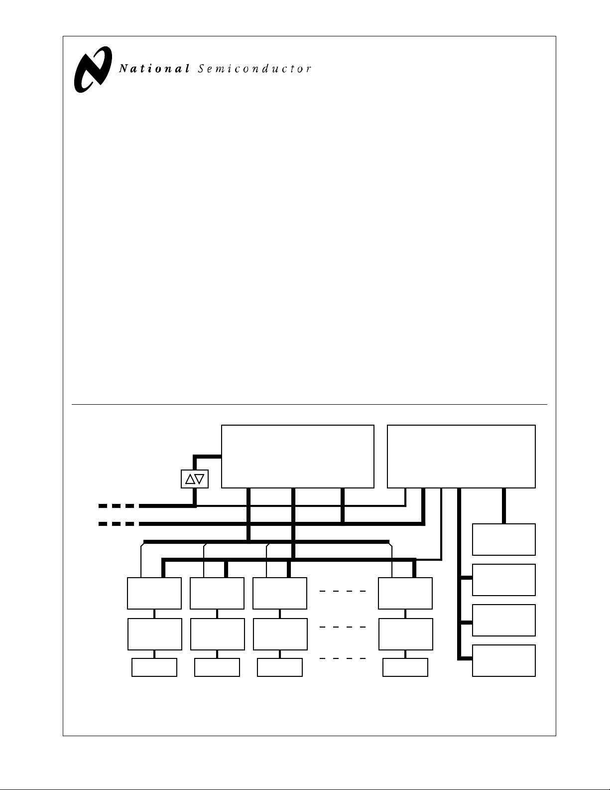
System Diagram
DP83850C
100 Mb/s
Repeater Interface Controller
(100RIC8)
Features
■ IEEE 802.3u repeater and management compatible
■ Supports Class II TX translational repeater and Class I
T4 repeater
■ Supports 12 network connections (ports)
■ Up to 31 repeater chips cascadable for larger hub appli-
cations (up to 372 ports)
■ Separate jabber and partition state machines for each
port
■ Management interface to DP83856 allows all repeater
MIBs to be maintained
■ Large per-port management counters - reduces management CPU overhead
■ On-chip elasticity buffer for PHY signal re-timing to the
DP83850C clock source
■ Serial register interface - reduces cost
■ Physical layer device control/status access available via
the serial register interface
■ Detects repeater identification errors
■ 132 pin PQFP package
DP83856
100 Mb/s
Repeater Information Base
(100RIB)
™
)
Inter Repeater Bus
(IR_COL, IR_DV)
Management Bus
RX Enable [11..0]
MII
DP83840A
100 PHY
#0
DP83223
100BASE-X
100Mb/s
Ethernet
Ports
Note: The above system diagram depicts the repeater configured in 100BASE-TX mode.
FAST® is a registered trademark of Fairchild Semiconductor Corporation.
TRI-STATE
™
is a trademark of National Semiconductor Corporation.
100RIC
© 1998 National Semiconductor Corporation
Transceiver
Port 0
®
is a registered trademark of National Semiconductor Corporation.
DP83840A
100 PHY
#1
DP83223
100BASE-X
Transceiver
Port 1
DP83840A
100 PHY
#2
DP83223
100BASE-X
Transceiver
Port 2
DP83840A
100 PHY
#11
DP83223
100BASE-X
Transceiver
Port 11
Statistics
(TXD[3:0], TX_ER, TX_RDY)
SRAM
Management
Program
Memory
Management
I/O Devices
www.national.com
CPU
Page 2
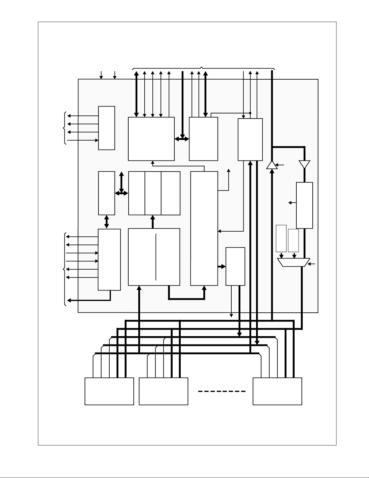
Block Diagram
EE_CK
EE_CS
EE_DI
EE_DO
EEPROM INTERFACE
LCK
/RST
EEPROM
ACCESS LOGIC
Other Registers
MUX
REGISTER
MANAGEMENT & INTER REPEATER BUS INTERFACE
M_CK
/M_ER
/M_DV
MD[3:0]
COUNTERS
LATE EVENT
RID_ER
RID[4:0]
LOGIC
MANAGEMENT
Active Port #
COUNTERS
SHORT EVENT
REGISTERS
CONFIG./STATUS
IRD_ODIR
/IR_BUS_EN
IR_VECT[4:0]
DISTRIBUTED
ARBITRATION
LOGIC
/IR_COL_IN
State
PORT_COL[11:0]
/ACTIVEO
/IR_COL_OUT
SELECT/COL.
DETECT LOGIC
IRD[3:0], /IRD_ER, IRD_CK, /IRD_V
TX/T4
100RIC
DP83850C
EB_ERROR
BUFFER
ELASTICITY
RDIR
RDIO
RDC
/SDV
GRDIO
BRDC
PART[5:0]
ACCESS LOGIC
SERIAL REGISTER
PER PORT
JABBER CONTROL
CRS[11:0]
SERIAL REGISTER/MANAGEMENT INTERFACE
RXE[0]
CRS[0]
TXE[0]
#0
PHY
PER PORT
COUNTERS
COL & PART
STATE MACHINES
& AUTO-PARTITION
ACTIVITY[11:0]
RXD[3:0], RX_ER, RXC, RX_DV
TXD[3:0], TX_ER
TXE[11:0]
RXE[11:0]
CRS[11:0]
CRS[1]
TXE[1]
RXE[1]
#1
PHY
STATE
MACHINE
REPEATER
TXE
CONTROL
TX_RDY
TXE[11:0]
RXE[11:0]
CRS[11:0]
CRS[11]
Jam
Pre-amble
Generation
Regeneration
Repeater
State Machine
RXD[3:0],RX_ER, RXC, RX_DV
TXE[11]
RXE[11]
PHY
TXD[3:0], TX_ER
#11
PHYSICAL LAYER INTERFACE
2 www.national.com
Page 3

Table of Contents
1.0 Pin Connection Diagram . . . . . . . . . . . . . . . . . . . . . . . .4
1.1 Pin Table . . . . . . . . . . . . . . . . . . . . . . . . . . . . . . . .5
2.0 Pin Description . . . . . . . . . . . . . . . . . . . . . . . . . . . . . . . .6
2.1 Physical Layer Interface . . . . . . . . . . . . . . . . . . . . 6
2.2 Inter Repeater and Management Bus Interface . . .7
2.3 EEPROM Interface . . . . . . . . . . . . . . . . . . . . . . . .8
2.4 Miscellaneous . . . . . . . . . . . . . . . . . . . . . . . . . . . . 8
2.5 Pin Type Designation . . . . . . . . . . . . . . . . . . . . . . .9
3.0 Functional Description . . . . . . . . . . . . . . . . . . . . . . . . .10
3.1 Repeater State Machine . . . . . . . . . . . . . . . . . . . 10
3.2 RXE Control . . . . . . . . . . . . . . . . . . . . . . . . . . . . .10
3.3 TXE Control . . . . . . . . . . . . . . . . . . . . . . . . . . . . .10
3.4 Data Path . . . . . . . . . . . . . . . . . . . . . . . . . . . . . . .10
3.5 Elasticity Buffer . . . . . . . . . . . . . . . . . . . . . . . . . . 10
3.6 Jabber Protection State Machine . . . . . . . . . . . . .11
3.7 Auto-Partition State Machine . . . . . . . . . . . . . . . . 11
3.8 Inter Repeater Bus Interface . . . . . . . . . . . . . . . .11
3.9 Management Bus . . . . . . . . . . . . . . . . . . . . . . . . .12
3.10 Management Event Flags and Counters . . . . . . .12
3.11 Serial Register Interface . . . . . . . . . . . . . . . . . . .12
3.12 Jabber/Partition LED Driver Logic . . . . . . . . . . . . 15
3.13 EEPROM Serial Read Access . . . . . . . . . . . . . . .15
4.0 Registers . . . . . . . . . . . . . . . . . . . . . . . . . . . . . . . . . . . 16
4.1 Page 0 Register Map . . . . . . . . . . . . . . . . . . . . . 16
4.2 Page 1 Register Map . . . . . . . . . . . . . . . . . . . . . 17
4.3 Configuration Register (CONFIG) . . . . . . . . . . . 17
4.4 Page Register (PAGE) . . . . . . . . . . . . . . . . . . . . 18
4.5 Partition Status Register (PARTITION) . . . . . . . 18
4.6 Jabber Status Register (JABBER) . . . . . . . . . . . 18
4.7 Administration Register (ADMIN) . . . . . . . . . . . . 19
4.8 Device ID Register (DEVICEID) . . . . . . . . . . . . . 19
4.9 Hub ID 0 Register (HUBID0) . . . . . . . . . . . . . . . 19
4.10 Hub ID 1 Register (HUBID1) . . . . . . . . . . . . . . . 20
4.11 Port Management Counter Registers . . . . . . . . . 20
4.12 Silicon Revision Register (SIREV) . . . . . . . . . . . 20
5.0 DP83850C Applications . . . . . . . . . . . . . . . . . . . . . . . 21
5.1 MII Interface Connections . . . . . . . . . . . . . . . . . . 21
5.2 Repeater ID Interface . . . . . . . . . . . . . . . . . . . . . 21
5.3 Inter Repeater Bus Connections . . . . . . . . . . . . 21
5.4 DP83856 100RIB Connections . . . . . . . . . . . . . . 25
5.5 Port Partition and Jabber Status LEDs . . . . . . . . 26
6.0 A.C. and D.C. Specifications . . . . . . . . . . . . . . . . . . . 27
6.1 D.C. Specifications . . . . . . . . . . . . . . . . . . . . . . . 27
6.2 A.C. Specifications . . . . . . . . . . . . . . . . . . . . . . . 28
7.0 Physical Dimensions . . . . . . . . . . . . . . . . . . . . . . . . . 37
3 www.national.com
Page 4
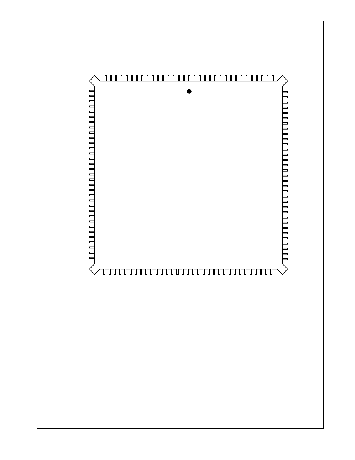
1.0 Pin Connection Diagram
VCC
GND
/IRD_V
IRD3
IRD2
IRD1
IRD0
IRD_CK
VCC
GND
TX_ER
TXD0
TXD1
TXD2
TXD3
VCC
GND
/IR_ACTIVE
/IR_COL_OUT
/IR_COL_IN
IR_VECT0
IR_VECT1
IR_VECT2
IR_VECT3
IR_VECT4
VCC
GND
MD0
MD1
MD2
MD3
VCC
GND
IRD_ODIR
/IRD_ER
RSM3/RXECONFIG
RXD0
RXD1
RXD2
RXD3
RX_DV
RX_ER
RXC
GND
VCC
CRS0
CRS1
CRS2
CRS3
CRS4
CRS5
CRS6
CRS7
CRS8
CRS9
CRS10
CRS11
RXE0
RXE1
RXE2
RXE3
GND
VCC
RXE4
RXE5
RXE6
8
9
6
7
16
17
15
14
18
19
20
21
22
23
24
25
26
27
28
29
30
31
32
33
34
35
36
37
38
39
40
41
42
43
44
45
46
47
48
49
50
51
DP83850CVF
54
52
53
10
11
12
13
Repeater Interface Controller
132 pin PQFP
58
57
56
55
62
61
60
59
2
3
4
5
1
100 Mb/s
TX/T4
(100RIC)
(top view)
67
66
65
64
63
130
131
132
69
68
128
129
72
71
70
124
125
126
127
74
73
122
123
78
77
76
75
118
119
120
121
79
117
116
/M_DV
115
M_CK
/M_ER
114
113
/IR_BUS_EN
112
VCC
111
GND
/ACTIVE0
110
/SDV
109
RDIR
108
107
RDIO
106
RDC
105
GRDIO
104
BRDC
/RST
103
VCC
102
101
GND
LCK
100
99
RID0
98
RID1
97
RID2
96
RID3
95
VCC
94
GND
93
RID4
92
RID_ER
91
PART0
90
PART1
89
PART2
88
PART3
87
PART4
86
VCC
85
GND
84
PART5
83
82
81
80
RXE7
RXE8
RXE9
RXE10
RXE11
GND
VCC
TXE0
TXE1
TXE2
TXE3
TXE4
TXE5
TXE6
TXE7
GND
VCC
Order Number DP83850CVF
NS Package Number VF132A
4 www.national.com
TXE8
TXE9
TXE10
TXE11
RSM0
RSM1
RSM2
GND
TX_RDY
VCC
EE_SK
EE_CS
EE_DI
EE_DO
MODE0
MODE1
Page 5

1.0 Pin Connection Diagram (Continued)
1.1 Pin Table
Pin Name Pin No. Section
/ACTIVEO 110 2.2
/IR_ACTIVE 132 2.2
/IR_BUS_EN 113 2.2
/IR_COL_IN 130 2.2
/IR_COL_OUT 131 2.2
/IRD_ER 19 2.2
/IRD_V 15 2.2
/M_DV 116 2.2
/M_ER 114 2.2
/RST 103 2.4
/SDV 109 2.2
BRDC 104 2.4
CRS[11:0] 41-30 2.1
EE_CK 79 2.3
EE_CS 78 2.3
EE_DI 81 2.3
EE_DO 80 2.3
GND 1, 8, 16, 28, 46, 56, 66,76, 85, 94, 101, 111, 117,123 N/A
GRDIO 105 2.4
IR_VECT[4:0] 125-129 2.2
IRD[3:0] 14-11 2.2
IRD_CK 10 2.2
IRD_ODIR 18 2.4
LCK 100 2.4
M_CK 115 2.2
MD[3:0] 119-122 2.2
MODE[1:0] 83-82 2.4
PART[5:0] 84, 87-91 2.4
RDC 106 2.2
RDIO 107 2.2
RDIR 108 2.4
RID[4:0] 93, 96-99 2.4
RID_ER 92 2.4
RSM[2:0] 74-72 2.4
RSM[3]/ RXECONFIG 20 2.4
RX_DV 25 2.1
RX_ER 26 2.1
RXC 27 2.1
RXD[3:0] 24-21 2.1
RXE[11:0] 55-48, 45-42 2.1
TX_ER 7 2.1
TX_RDY 75 2.1
TXD[3:0] 3-6 2.1
TXE[11:0] 71-68, 65-58 2.1
VCC 2, 9, 17, 29, 47, 57, 67, 77, 86, 95, 102, 112, 118, 124 N/A
5 www.national.com
Page 6

2.0 Pin Descriptions
2.1 Physical Layer Interface
Signal Name Type Active Description
RXD[3:0] I — Receive Data: Nibble data inputs from each Physical layer chip. Up to 12 ports are sup-
RXE[11:0] O, L high (low) Receive Enable: Asserted to the respective Physical Layer chip to enable its Receive
RX_DV I high Receive Data Valid: Asserted High when valid data is present on RXD[3:0].
RX_ER I high Receive Error: The physical Layer asserts this signal high when it detects receive error.
RXC I — Receive Clock: Recovered clock from the Physical Layer device. RXD, RX_DV, and
CRS[11:0] I high Carrier Sense: Asynchronous carrier indication from the Physical Layer device.
TXE[11:0] O, L high Transmit Enable: Enables corresponding port for transmitting data.
TX_RDY O, L high Transmit Ready: Indicates when a transmit is in progress. Essentially, this signal is the
TX_ER O, M high Transmit Error: Asserted high when a code violation is requested to be transmitted.
TXD[3:0] O, H high Transmit Data: Nibble data output to be transmitted by each Physical Layer device.
Note: A table showing pin type designation is given in section 2.5
ported.
Note: Input buffer has a weak pull-up.
Data. These pins are either active high or active low depending on the polarity of RSM3
pin as shown below:
RXE[11:0] RSM3
Active High Unconnected or pulled high
Active Low Pulled down
Note: To ensure that during idle, when 100PHYs TRI-STATE®, this signal is NOT interpreted as “logic one” by the repeater, a 1kΩ pull down resistor must be placed on this
pin. The location on this pull down should be between the repeater and the nearest tristateable component to the repeater.
When this signal is asserted, the 100PHY (TX or T4) device indicates the type of error
on RXD[3:0] as shown below. Note that this data is passed only to the Inter Repeater
Bus, and not onto the TX Bus:
RX_ER RXD[3:0] Receive Error Condition
0 data Normal data reception
1 0h Symbol code violation
1
1h
1
Elasticity Buffer Over/Under-run
1 2h Invalid Frame Termination
1
1
1
The 100PHY must be configured with the Elasticity Buffer bypassed; hence this error
3h
4h
2
Reserved
2
10Mb Link Detected
code will never be generated.
2
These error codes will only appear when CRS from the 100PHY is not asserted. Since
the DP83850C only enables a 100PHY when its CRS is asserted, these error codes will
never be passed through the chip.
Note: Input buffer has a weak pull-down.
RX_ER are generated from the falling edge of this clock.
Note: Input buffer has a weak pull-down.
logical 'OR' of all TXEs.
6 www.national.com
Page 7

2.0 Pin Descriptions (Continued)
2.2 Inter Repeater and Management Bus Interface
Signal Name Type Active Description
IRD[3:0] I/O/Z, M — Inter Repeater Data: Nibble data input/output. Transfers data from the “active”
/IRD_ER I/O/Z, M low Inter Repeater Data Error: This signal carries the RX_ER state across the Inter Re-
/IRD_V I/O/Z, M low Inter Repeater Data Valid: This signal carries the inverted RX_DV state across the
IRD_CK I/O/Z, M — Inter Repeater Data Clock: All Inter Repeater signals are synchronized to the rising
IRD_ODIR O, L high Inter Repeater Data Outward Direction: This pin indicates the direction of data for
/IR_ACTIVE I/O/OC, M low Inter Repeater Activity: This “open-collector” type output is asserted when the re-
/IR_COL_IN I low Inter Repeater Collision In: Indication from another DP83850C that it senses two or
/IR_COL_OUT O/OC, M low Inter Repeater Collision Out: Asserted when the DP83850C senses two or more
IR_VECT[4:0] I/O/OC, M high Inter Repeater Vector: When the repeater senses at least one of its ports active, it
MD[3:0] I/O/Z, M high Management Data: Outputs management information for the DP83856 manage-
/M_DV I/O/Z, M low Management Data Valid: Asserted when valid data is present on MD[3:0].
M_CK I/O/Z, M — Management Clock: All data transfers on the management bus are synchronize to
/M_ER I/O/Z, M low Management Error: Asserted when an Elasticity Buffer overrun or under-run error
DP83850C to all other “inactive” DP83850Cs. The bus master of the IRD bus is determined by IR_VECT bus arbitration.
Note: Input buffer has a weak pull-up.
peater bus. Used to track receive errors from the physical layer in real-time
Inter Repeater bus. It is used to frame good packets.
Note: A recommended 1.5K pull-up prevents first repeated packet corruption .
edge of this clock.
Note: Input buffer has a weak pull-up.
an external transceiver. It is HIGH when IRD[3:0], /IRD_V, /IRD_CK, and /IRD_ER
are driven out towards the Inter Repeater bus, and LO W when data is being received
from the bus.
peater senses network activity.
Note: Input buffer has a weak pull-up.
more ports receiving or another DP83850C has detected a collision.
Note: Input buffer has a weak pull-up.
ports receiving or non-idle, either 1) within this DP83850C or 2) in another
DP83850C, using the IR_VECT number to decide (the IR_VECT number read will differ from the number of this DP83850C if another device is active).
drives its unique vector (from RID[4:0]) onto these pins. If the vector v alue read bac k
differs from its own (because another vector is being asserted by another device),
then this DP83850C will:
1) not drive IRD_ODIR signal and,
2) the IRD[3:0], /IRD_ER, /IRD_V, and IRD_CK signals will be placed in TRI-STATE
mode.
Howev er, if the value read back is the same as its own RID number, this DP83850C
will continue to drive the Inter Repeater bus signals. Note that these v ectors are driven onto the bus for the duration of /ACTIVEO assertion.
Note: Input buffer has a weak pull-up.
ment chip. During packet reception the DP83850C drives its RID number and the port
number of the receiving port onto this bus.
Note: Input buffer has a weak pull-up.
Note: Input buffer has a weak pull-up.
the rising edge of this clock.
Note: Input buffer has a weak pull-up.
has been detected.
Note: Input buffer has a weak pull-up.
7 www.national.com
Page 8

2.0 Pin Descriptions (Continued)
Signal Name Type Active Description
/IR_BUS_EN O,L low Inter-Repeater Bus Enable: This signal is asserted at all times (either when the
RDIO I/O/Z, L — Register Data I/O: Serial data input/output transfers data to/from the internal regis-
RDC I — Register Data Clock: All data transfers on RDIO are synchronized to the rising edge
/SDV I low Serial Data Valid: Asserted when a valid read or write command is present. Used to
/ACTIVEO O/OC, M low Active Out: Enable for the IR_VECT[4:0] and /IR_ACTIVE signals. Used in multi-
Note: A table showing pin type designation is given in section 2.5
100RIC is driving the bus or receiving from the bus) and it is deasserted only when
the 100RIC switches direction from an input (receiving) mode to an output (driving)
mode. After this switch, this signal becomes asserted again.
ters. Serial protocol conforms to the IEEE 802.3u MII (Media Independent Interface)
specification.
Note: Input buffer has a weak pull-up.
of this clock. RDC is limited to a maximum frequency of 2.5 MHz. At least 3 cycles
of RDC must be provided during assertion of /RST (pin 103) to ensure proper reset
of all internal blocks.
detect disconnection of the management bus so that synchronization is not lost. If not
used, tie this pin to GND.
Note: Input buffer has a weak pull-up.
DP83850C systems to enable the external buff ers driving these Inter Repeater Bus
signals.
A pull up of 680 1/2 must be used with this signal.
2.3 EEPROM Interface
Signal Name Type Active Pin Description
EE_CS O, L high EEPROM Chip Select: Asserted during reads to EEPROM.
EE_CK O, L - EEPROM Serial Clock: Local Clock ÷ 32 = 0.78125MHz
EE_DO I - EEPROM Serial Data Out: Connected to the serial data out of the EEPROM.
EE_DI O, L - EEPROM Serial Data In: Connected to the serial data in of the EEPROM.
2.4 Miscellaneous
Signal Name Type Active Pin Description
LCK I — Local Clock: Must be 25 MHz ± 50ppm. Used for TX data transfer to Physical Layer
RID[4:0] I — Repeater Identification Number: Provides the unique vector for the IR_VECT[4:0]
/RST I low Reset: The chip is reset when this signal is asserted low.
GRDIO I/O/Z, L — Gated Register Data Input/Output: This I/O is a gated version of RDIO. When the
BRDC O, L — Buffered Register Data Clock: Buffered v ersion of RDC. Allows more devices to be
RDIR O, L high Register Data Direction: Direction signal for an external bi-directional buffer on the
devices, TX Bus data transfers and DP83850C internal state machines.
signals used in Inter Repeater bus arbitration. These bit are also used to uniquely identify this chip for serial register accesses. The RID value is latched when reset is deasserted.
Note: The arbiter cannot use the value 1Fh as its arbitration vector. This is the
IR_VECT[4:0] bus idle state, therefore RID[4:0] must never be set to this value.
“phy_access” bit in the CONFIG register is set high, the RDIO signal is passed through
to GRDIO for accessing the physical layer chips.
Note: Input buffer has a weak pull-up.
chained on the MII serial bus.
RDIO signal.
0 = RDIO data flows into the DP83850C
1 = RDIO data flows out of the DP83850C
Defaults to 0 when no register access is present.
8 www.national.com
Page 9

2.0 Pin Descriptions (Continued)
Signal Name Type Active Pin Description
PART[5:0] O, L — Partition: Used to indicate each port's Jabber and Partition status. PART[3:0] cycle
RID_ER O, L high Repeater ID Error: This pin is asserted under the conditions which set the RID_error
RSM[3]
/RXECONFIG
RSM[3]
RSM[2:0]
MODE[1:0] I — Mode Inputs: The 100RIC may be configured in the following modes:
Note: A table showing pin type designation is given in section 2.5
I/O, L — Repeater State Machine Output/ RXE Polarity: This pin is an input during reset and
I/O, L O, L — Test Outputs indicating the state of the Repeater State Machine.
through each port number (0-11) continuously. PART[4] indicates the Partition status
for each port (1 = Port Partitioned). PART[5] indicates the Jabber status for each port
(1 = Port Jabbering). These pins are intended to be decoded to drive LEDs.
bit in the DEVICEID register.
it is used to latch the desired polarity of RXE[11:0] signals.
When this pin is pulled high or it is unconnected, then the RXE signals become active
high. However, if this signal is pulled low, then the RXE signals become active low.
In all other non-reset times, this pin reflects the output of the Repeater State Machine.
RSM[3:0] State
0 idle
1 collision
2 one port left
3 repeat
4 noise
Other states are undefined.
MODE[1:0] Operation
0,0 No special modes selected
1,0 Test mode
0,1 Test mode
1,1 Preamble regeneration (T4) mode
2.5 Pin Type Designation
Pin Type Description
I Input Buffer
O Output Buffer, driven high or low at all times
I/O/Z Bi-directional Buffer with high impedance output
O/Z Output Buffer with high impedance capability
OC Open Collector like signals. These buffers are
either driven low or in a high-impedance state.
L Output low drive: 4 mA
M Output medium drive: 12 mA
H Output high drive : 24 mA
9 www.national.com
Page 10

3.0 Functional Description
The following sections describe the different functional
blocks of the DP83850C 100 Mb/s Repeater Interface Controller. The IEEE 802.3u repeater specification details a
number of functions a repeater system is required to perform. These functions are split between those tasks that
are common to all data channels and those that are specific to each individual channel. The DP83850C follows
this split task approach for implementing the required functions. Where necessary , the diff erence betw een the TX and
T4 modes is discussed.
3.1 Repeater State Machine
The Repeater State Machine (RSM) is the main block that
governs the overall operation of the repeater. At any one
time, the RSM is in one of the following states: Idle,
Repeat, Collision, One Port Left, or Noise.
3.1.1 Idle State
The RSM enters this state after reset or when there is no
activity on the network and the carrier sense is not present.
The RSM exits from this state if the above conditions are
no longer true.
3.1.2 Repeat State
This state is entered when there is a reception on only one
of the ports, port N. While in this state, the data is transmitted to all the ports except the receiving port (por t N). The
RSM either returns to Idle state when the reception ends,
or transitions to Collision state if there is reception activity
on more than one port.
3.1.3 Collision State
When there is receive activity on more than one port of the
repeater, the RSM moves to Collision state. In this state,
transmit data is replaced by Jam and sent out to all ports
including the original port N.
There are two ways for the repeater to leave the Collision
state. The first is when there is no receive activity on any
of the ports. In this case, the repeater moves to Idle state.
The second is when there is only one port experiencing
collision in which case the repeater enters the One Port
Left state.
3.1.4 One Port Left State
This state is entered only from the Collision state. It guarantees that repeaters connected hierarchically will not jam
each other indefinitely. While in this state, Jam is sent out
to all ports except the port that has the receive activity. If
more receive activity occurs on any other port, then the
repeater moves to Collision state.
Otherwise, the repeater will transition to Idle state when the
receive activity ends.
3.1.5 Noise State
When there is an Elasticity Buffer overflow or underflow
during packet reception, then the repeater enters the Noise
state. During this state, the Jam pattern is sent to all transmitting ports. The repeater leaves this state by moving
either to the Idle state, if there is no receive activity on any
ports, or to the Collision state, if there is a collision on one
of its segments.
3.2 RXE Control
When only one port has receive activity, the RXE signal
(receive enable) is activated. If multiple ports are active
(i.e. a collision scenario), then RXE will not be enabled for
any port. The Port Select Logic asserts the open-collector
outputs /IR_COL_OUT and /IR_ACTIVE to indicate to
other cascaded DP83850Cs that there is collision or
receive activity present on this DP83850C.
The polarity of the RXE signal can be set through an external pull down resistor placed at the RSM[3] pin. That is, if
the RSM[3] pin is unconnected or pulled high, then the
RXE is active high and when the RSM[3] is pulled low, then
the RXE is active low.
3.3 TXE Control
This control logic enables the appropriate ports for data
transmission according to the four states of the RSM. For
example, during Idle state, no ports are enabled; during
Repeat state, all ports but port N are enabled; in Collision
state, all ports including port N are enabled ; during One
Port Left state, all ports except the port experiencing the
collision will be enabled.
3.4 Data Path
After the Port Selection logic has enabled the active port,
receive data (RXD), receive clock (RXC), receive error
(RX_ER) and receive data valid (RX_DV) will flow through
the chip from that port out onto the Inter Repeater (IR) bus
if no collisions are present. The signals on the IR bus flow
either in to or out of the chip depending upon the
Repeater’s state.
If the DP83850C is currently receiving and no collisions are
present, the IR signals flow out of the chip. The
DP83850C's Arbitration Logic guarantees that only one
DP83850C will gain ownership of the IR bus. In all other
states, the IR signals are inputs.
When IR signals are inputs, the signals flow into the Elasticity Buffer (EB). Here, the data is re-timed and then sent
out to the transmit ports. The Transmit Control logic determines which ports are enabled for data transmission.
If a collision occurs, a Jam pattern is sent out from the EB
instead of the data. The Jam pattern (3,4,3,4,..... from the
DP83850C, encoded by the Physical Layer device as
1,0,1,0,.....) is transmitted for the duration of the collision
activity.
If the repeater is configured in the preamble regeneration
mode (T4 mode), approximately 12 clock cycles after the
assertion of /IR_ACTIVE (indicating a packet reception on
a segment), the 100RIC begins to transmit the preamble
pattern onto the other network segments. While the preamble is being transmitted, the EB monitors the received
clock and data signals. When the start of the frame delimiter "SFD" is detected, the received data stream is written
into the EB. After this point, data from the EB is sent out to
the Transmit interface. The preamble is always generated
in its entirety (i.e. fifteen 5’s and one D) even if a collision
occurs.
3.5 Elasticity Buffer
The elasticity buffer, or a logical FIFO buffer, is used to
compensate for the variations and timing differences
between the recovered Receive Clock and the local clock.
This buffer supports maximum clock skews of 200ppm for
the preamble regeneration (T4) mode, and 100ppm for the
TX mode, within a maximum packet size of 1518 bytes.
10 www.national.com
Page 11

3.0 Functional Description (Continued)
3.6 Jabber Protection State Machine
The jabber specification for 100BASE-T is functionally different than 10BASE-T.
In 10BASE-T, each port's Jabber Protect State machine
ensures that Jabber transmissions are stopped after 5ms
and followed by 96 to 116 bit times silence before the port
is re-enabled.
In 100BASE-T, when a por t jabbers, its receive and transmit ports are cutoff until the jabber activity ceases. All other
ports remain unaffected and continue normal operation.
The 100BASE-T Jabber Protect Limit (that is, the time for
which a port can jabber until it is cutoff) for the DP83850C
is reached if the CRS is active for more than 655µs.
A jabbering port that is cut off will be re-enabled when the
jabber activity ceases and the IDLE line condition is
sensed.
3.7 Auto-Partition State Machine
In order to protect the network from a port that is experiencing excessive consecutive collisions, each port must
have its own auto-partition state machine.
A port with excessive consecutive collisions will be partitioned after a programmed number of consecutive collisions occur on that port. Transmitting ports will not be
affected.
The DP83850C has a configuration bit that allows the user
to choose how many consecutive collisions a port should
experience before partitioning. This bit can be set for either
32 or 64 consecutive collisions. The IEEE802.3u
100BASE-T standard specifies the consecutive collisions
limit as greater than 60. A partitioned port will be reconnected when a collision-free packet of length 512 bits or
more (that is, at least a minimum sized packet) is transmitted out of that port.
The DP83850C also provides a configuration bit that disables the auto-partition function completely.
3.8 Inter Repeater Bus Interface
The Inter Repeater bus is used to connect multiple
DP83850Cs together to form a logical repeater unit and
also to allow a managed entity. The IR bus allows received
data packets to be transferred from the receiving
DP83850C to the other DP83850Cs in the system. These
DP83850Cs then send the data stream to their transmit
enabled ports.
Notification of collisions to other cascaded DP83850Cs is
as important as data transfer across the network. The arbitration logic asynchronously determines if more than one
100RIC, cascaded together, are receiving simultaneously.
The IR bus has a set of status lines capable of conveying
collision information between DP83850Cs to ensure their
main state machines operate in the appropriate manner.
The IR bus consists of the following signals:
■ Inter Repeater Data. This is the transfer data, in nibble
format, from the active DP83850C to all other cascaded
DP83850Cs.
■ Inter Repeater Data Error. This signal carries the receive error status from the physical layer in real-time.
■ Inter Repeater Data Valid. This signal is used to frame
good packets.
■ Inter Repeater Data Clock. All IR data is synchronized
to this clock.
■ Inter Repeater Data Outward Direction. This pin indicates the direction of the data flow with respect to the
DP83850C. When the DP83850C is driving the IR bus
(i.e. it contains port N) this signal is HIGH and when the
DP83850C is receiving data from other DP83850Cs
over the IR bus this signal is LOW.
■ Inter Repeater Bus Enable. This signal (connected to
the /ENABLE pin of the external transceivers on the IR
bus) is used in conjunction with the IRD_ODIR signal
(connected to the DIR pin of the transceivers) to TRISTATE these transceivers during the change of direction
from input to output, or vice versa. This signal is always
active allowing the IR bus signals to pass through the
transceivers into or out of the 100RIC. However when
the 100RIC switches from input mode (IRD_ODIR=0) to
output mode (IRD_ODIR=1), the /IR_BUS_EN signal is
deasserted allowing the transceivers to TRI-STATE during the direction change. After this turn-around, this
signal is asserted back again. (IRD_ODIR assertion
(high) to /IR_BUS_EN low timing is a minimum of 0.1 ns.
and a maximum of 1.0. The time from /IR_BUS_EN
(high) to the IRD_ODIR high is a minimum of 10 ns. and
a maximum of 20 ns. In addition, /ACTIVEO assertion
(low) to /IR_BUS_EN high timing is a maximum of 1.0
ns.)
■ Inter Repeater Activity. When there is network activity
the DP83850C asserts this output signal.
■ Inter Repeater Collision Output. If there are multiple receptions on ports of a DP83850C or if the DP83850C
senses concurrent activity on another DP83850C it asserts this output.
■ Inter Repeater Collision Input. This input indicates that
one of the cascaded DP83850Cs is experiencing a collision.
■ Inter Repeater Vector. When there is reception on a port
the DP83850C drives a unique vector onto these lines.
The vector on the IR bus is compared with the Repeater
ID (RID). The DP83850C will continue to drive the IR
bus if both the vector and RID match.
The following figure shows the conditions that cause an
open collector vector signal to be asserted on the backplane bus.
RID[n]=0
&
/ACTIVEO=0
/IR_VECT[n]
Figure 1. Open Collector /IR_VECT[n]
As seen, if the RID[n]=1, and the repeater is receiving on a
port, then the /IR_VECT[n] value would be 1 due to the
pull-up on this pin. In the case that RID[n]=0, then a zero is
driven out on the /IR_VECT[n] signal.
As an example assume that two repeaters with RIDs equal
to RID #1=00010 and RID #2=00011 are connected
through the Inter-RIC bus. The following diagrams depict
the values of /IR_VECT signals over the backplane.
■ Active Output. This signal is asserted by a DP83850C
when at least one of its ports is active. It is used to enable
external bus transceivers.
11 www.national.com
Page 12
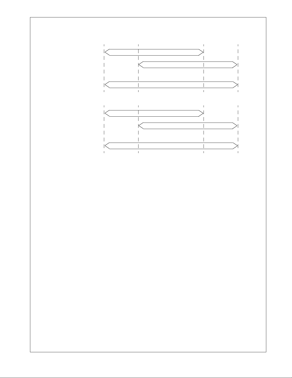
3.0 Functional Description (Continued)
Activity on the 100RIC
with RID=00010
Activity on the 100RIC
with RID=00011
/IR_Vect value on
the backplane
Activity on the 100RIC
with RID=00011
Activity on the 100RIC
with RID=00010
/IR_VECT value on
the backplane
Figure 2. RID to /IR_VECT Mapping
RID=00010
RID=00011
3.9 Management Bus
The task of network statistics gathering in a repeater system is divided between the DP83850C and DP83856
devices. Together, these devices collect all the required
management information (compliant to IEEE 802.3u clause
30) associated with a packet.
Each time a packet is received by a DP83850C, it drives
the device and the port number onto the management bus
in 3 contiguous nibbles of data.
During a single reception, only one DP83850C drives this
information onto the management bus. During a collision,
the management bus will TRI-STATE (because the information on this bus becomes invalid).
The first nibble of management data contains the least significant 4 bits of the RID number, the second contains the
most significant bit of the RID number and the third contains the number of the receiving port.
When the 100RIC is not receiving a packet, it monitors the
RID numbers from other 100RICs. If there is a match
between any of these numbers and 100RIC’s own RID,
then a RID contention error signal (RID_ER) is asserted.
The management bus also indicates whether an elasticity
buffer error (due to under-run or over-run) has occurred by
asserting the /M_ER signal.
3.10 Management Event Flags and Counters
Repeater management statistics are supported either
directly by using the DP83850C's on-chip event flags and
counters, or indirectly, by the DP83850C providing the
information to the DP83856 via the management and
transmit bus.
Management information is maintained within the
DP83850C in two ways: event flags and counters.
Collision
RID=00011
00010 0001100010
Collision
RID=00010
00010 0001000011
3.10.1 Event Flags
These are the events that provide a snapshot of the operation of the DP83850C. These events include:
■ Auto-Partition State, indicating whether a port is currently partitioned.
■ Jabber State, indicating whether a port is in jabber state.
■ Administration State, indicating if a port is disabled.
3.10.2 Event Counters
The event counters maintain the statistics for events that
occur too frequently for polled flags, or are collision oriented. Each port has its own set of event counters that
keep track of the following events:
■ Port Collisions. A 32-bit counter providing the number of
collision occurrences on a port.
■ Port Partitions. A 16-bit counter indicating the number of
times that the port has partitioned.
■ Late Events. A 32-bit counter indicating the number of
times that a collision took place after 512 bit times (nominal). In the case of late events, both the late event and
the collision counters will be incremented.
■ Short Events. A 32-bits wide counter indicating the number of packets whose length is 76 bits (nominal) or less.
One port left
One port left
3.11 Serial Register Interface
The DP83850C has 64 registers held in two pages of 32
(Register Page 0 and Register Page 1). The registers are
16 bits wide. Only one page of registers can be accessed
at a time.
After power-up and/or reset, the DP83850C defaults to
Register Page 0. Register P age 1 can be accessed by writing 0001h to the PAGE register in Register Page 0, whereupon further accesses will be to Register Page 1.
12 www.national.com
Page 13

3.0 Functional Description (Continued)
Subsequently writing 0000h to the PAGE register in Register Page 1 switches the registers back to Register Page 0.
All accesses to DP83850C registers and counters, and to
the connected Physical Layer devices (via the DP83850C),
are performed serially using the RDIO and RDC pins. The
RDC clock is limited to a frequency no greater than
2.5MHz. This interface implements the serial management
protocol defined by the MII specification, IEEE 802.3u
clause 22. The protocol uses bit streams with the following
format:
For Read operation: <start><opcode><device addr><reg
addr> [turnaround] 0<data>.
For Write operation: <start><opcode><device addr><reg
addr> <10><data>.
This protocol allows for up to 32 devices (DP83850Cs or
other MII compliant devices) to be connected, each with a
unique address and up to 32 16-bit registers. Devices are
cascaded on the RDIO and RDC signals.
Since the RDIO pin is shared for both read and write operations, it must only be driven at the proper time. The serial
protocol assumes that there is only one master (generally,
the management entity's processor) and one or more slave
devices (generally, the Physical Layer or DP83850C chips).
The master drives RDIO at all times except when, during a
slave read operation, the addressed slave places the serialized read data onto the RDIO line after the line turnaround field's first bit.
For unmanaged systems that do not use the DP83856
100RIB device for repeater management, it is important to
provide the 100RIC with a minimum of 3 cycles of RDC
during device reset. If the minimum number of cycles of
RDC is not provided, the Serial Register Access Logic
block may not be properly reset and as a result RDIO may
not function properly. The 100RIB provides continuous
RDC cycles, and eliminates this concern.
The fields of the protocol are defined in Table 3-1. In order
for the protocol to work, all serial logic must first be “synchronized” to incoming data. A preamble of 32 consecutive
1's transmitted before the <start> field ensures "data lock".
13 www.national.com
Page 14

3.0 Functional Description (Continued)
≈ ≈
100PHY
DP83840A
Addr. = 11011
372 ports if required.
DP83856 100RIB. Another
Up to 16 DP83850C 100RICs
with 12 ports each = 192 ports per
Management CPU Bus
I/O
Management
Code
Program
CPU
Management
DP83850C 100RICs with up to
DP83856 100RIB device can be
added to control up to a total of 31
SRAM
Statistics
RDC
100RIB
DP83856
RDIO
≈
RDIO
≈
RDC
phy_access = 0
Addr. = 01111
100RIC
DP83850C
phy_access = 1
Addr. = 00001
100RIC
DP83850C
GRDIO
≈ ≈
GRDIO
BRDC
BRDC
100PHY
DP83840A
Addr. = 10001
100PHY
DP83840A
Addr. = 10000
100PHY
DP83840A
Addr. = 11011
100PHY
DP83840A
Addr. = 10001
100PHY
DP83840A
Addr. = 10000
100PHY
DP83840A
Addr. = 11011
≈ ≈
phy_access = 0
GRDIO
Addr. = 00000
100RIC
DP83850C
Figure 3. Serial Management Addressing Scheme
14 www.national.com
BRDC
100PHY
DP83840A
Addr. = 10001
100PHY
DP83840A
Addr. = 10000
Page 15

3.0 Functional Description (Continued)
This preamble only needs to be sent once (at reset). From
then on, the <start> field lets the receive logic know where
the beginning of the data frame occurs.
To access the Physical Layer devices via the serial bus, the
DP83850C has a “phy_access” mode. When in this mode,
the register data input/output (RDIO) is gated to the
GRDIO pin. This signal is connected to the serial data pins
of the Physical Layer devices.
In this mode the buffers which drive RDIO and GRDIO will
turn on in the appropriate direction for each serial access.
In order to avoid possible contention problems, the user
must ensure that only one DP83850C at a time has the
"phy_access" bit set. The CONFIG register contains the
“phy_access” bit, which can be set or cleared at any time.
Figure 3 shows a possible system implementation of the
RDIO/GRDIO connection scheme. In this example, the
DP83850C with address 00001 has its "phy_access" bit
set, allowing its twelve DP83840 PHY devices to be
accessed by the DP83856 100RIB.
Table 1. Serial Register Interface Encoding
Field Encoding Description
<start> 01 Indicates the beginning of an opcode operation.
<opcode> 10 Read
01 Write
all others Reserved
<reg addr> 00000 - 11111 Five bits are provided to address up to 32 16-bit registers.
<device addr> 00000 - 11111 Five bits are provided to address up to 32 devices.
MII serial management contention problems can be
avoided by keeping to the addressing convention shown in
Figure 3.
3.12 Jabber/Partition LED Driver Logic
This logic encodes the current auto-partition status (from
the PARTITION register) and the jabber status (from the
JABBER register), and outputs this information to
PART[5:0] pins. PART[3:0] cycles through each por t number and PART[5:4] indicates the port’s status. PART[5]
indicates the Jabber status for each port (0 = LED OFF, 1
=LED ON - Port Jabbering). PART[4] indicates the Partition
status for each port (0 = LED OFF, 1 = LED ON - Port AutoPartitioned).
The port number on PART[3:0] is cycled with a 25MHz.
External logic is required to decode the PART[5:0] outputs
and drive the Partition and Jabber LEDs. Multi-color LEDs
could be driven with the appropriate logic if required.
One possible implementation of a DP83850C Port Partition
and Jabber Status LED scheme is given in section 5.5.
EE_CS
EE_DI
EE_DO
3.13 EEPROM Serial Read Access
After reset is de-asserted, the DP83850C will serially read
an NM93C06 EEPROM (or equivalent). Only the first 32bits starting from address 0 will be read. Write access is
not provided. The data is written to registers HUBID0 and
HUBID1. The first bit read is written to HUBID0[0]; the last
bit read will be written to HUBID1[15].
The DP83850C EEPROM interface implements the serial
protocol as shown in Figure 3. The DP83850C will issue
two read commands to obtain the 32-bit ID. The serial
clock, EE_CK will be continuous. For more explicit timing
diagrams please refer to the NM93C06 datasheet.
<1...10><00000><1...> <1...0><00001><1...>
<0><D15..D0>
Figure 4. Serial EEPROM Access Protocol
<0><D31..D16>
The NM93C06 EEPROM must be pre-programmed with
the HUBID value prior to fitting the device to the circuit
since the DP83850C does not support programming of this
device in circuit.
15 www.national.com
Page 16

4.0 Registers
The DP83850C has 64 registers in 2 pages of 32 16-bit registers. At power-on and/or reset, the DP83850C defaults to
Page 0 registers. The register page can be changed by writing to the PAGE register in either register page. The register
page maps are given in sections 4.1 and 4.2, followed by a detailed description of the registers in sections 4.3 to 4.12.
4.1 Page 0 Register Map
Address
(hex)
0 CONFIG r/w Sets the DP83850C configuration.
1 PAGE r/w Selects either register page 0 or 1.
2 PARTITION read only Indicates Auto-Partitioning status.
3 JABBER read only Indicates Jabber status.
4 ADMIN r/w Port enable/disable, administration control/status.
5 DEVICEID r/w Accesses a) the DP83850C ID number configured externally on the RID[4:0] pins and
6 HUBID0 read only First 16 bits read from EEPROM.
7 HUBID1 read only Second 16 bits read from EEPROM.
8 P0_SE r/w Port 0: 32-bit ShortEvent counter (See access rules section 4.11).
9 P0_LE r/w Port 0: 32-bit LateEvent counter (See access rules section 4.11).
A P0_COL r/w Port 0: 32-bit Collision counter (See access rules section 4.11).
B P0_PART r/w Port 0: 16-bit Auto-Partition counter.
C P1_SE r/w Port 1: 32-bit ShortEvent counter (See access rules section 4.11).
D P1_LE r/w Port 1: 32-bit LateEvent counter (See access rules section 4.11).
E P1_COL r/w Port 1: 32-bit Collision counter (See access rules section 4.11).
F P1_PART r/w Port 1: 16-bit Auto-Partition counter.
10 - 13 P2_SE ...
14 - 17 P3_SE ...
18 - 1B P4_SE ...
1C - 1F P5_SE ...
Name Access Description
b) the last receiving port number. The DP83850C device number may be overwritten
after it has been latched at the end of reset: be careful not to have duplicate ID’s on
the same IR bus interface.
r/w Port 2 management counters (as per ports 0, 1 above).
P2_PART
r/w Port 3 management counters (as per ports 0, 1 above).
P3_PART
r/w Port 4 management counters (as per ports 0, 1 above).
P4_PART
r/w Port 5 management counters (as per ports 0, 1 above).
P5_PART
16 www.national.com
Page 17

4.0 Registers (Continued)
4.2 Page 1 Register Map
Address
(hex)
0 CONFIG r/w Sets the DP83850C configuration (same as page 0 CONFIG register).
1 PAGE r/w Select either register page 0 or 1.
2 - - Reserved
3 - - Reserved
4 SIREV read only Silicon revision code.
5 - 7 - - Reserved
8 - B P6_SE ...
C - F P7_SE ...
10 - 13 P8_SE ...
14 - 17 P9_SE ...
18 - 1B P10_SE ...
1C - 1F P11_SE ...
Name Access Description
r/w Port 6 management counters (as per ports 0, 1 above).
P6_PART
r/w Port 7 management counters (as per ports 0, 1 above).
P7_PART
r/w Port 8 management counters (as per ports 0, 1 above).
P8_PART
r/w Port 9 management counters (as per ports 0, 1 above).
P9_PART
r/w Port 10 management counters (as per ports 0, 1 above).
P10_PART
r/w Port 11 management counters (as per ports 0,1 above).
P11_PART
4.3 Configuration Register (CONFIG)
Page 0 Address 0h
Page 1 Address 0h
Bit Bit Name Access Bit Description
D15 - D6 reserved - For compatibility with future enhanced versions these bits must be written as zero.
D5 REGEN_PRE r/w Regenerate Preamble: This bit may be used to overwrite/change the repeater mode
D4 MGTEN r/w Management Enable: This bit enables all the management counters.
D3 COL_LIMIT32 r/w This bit configures the collision limit for Auto-Partitioning algorithm:
D2 DIS_PART r/w This bit disables the Auto-Partitioning algorithm:
They are undefined when read.
(TX or T4) that is set by the MODE[1:0] pins at power-up. If MODE[1:0] is 1, 1 then
this bit is set, otherwise this bit will be zero.
The time when the preamble is regenerated depends upon the type of the PHY (either TX or T4 PHYs) attached to the repeater. For a TX PHY, preamble is regenerated approximately 4 clocks (RXC) after the /IR_A CTIVE assertion, and for a T4 PHY,
preamble is regenerated approximately 12 clocks after the /IR_ACTIVE assertion.
0: Management Counters disabled (default).
1: Management Counters enabled.
Note: The management counters can only be reliably written to when they are dis-
abled.
0: Consecutive Collision Limit set to 64 consecutive collisions (default). A port will
be partitioned on the 65th consecutive collision.
1: Consecutive Collision Limit set to 32 consecutive collisions. A port will be parti-
tioned on the 33rd consecutive collision.
0: Auto-Partitioning is not disabled (default).
1: Auto-Partitioning is disabled.
17 www.national.com
Page 18

4.0 Registers (Continued)
Bit Bit Name Access Bit Description
D1 PHY_ACCESS r/w This bit allows the management agent to access the DP83840A PHY chip’s register
D0 RST_RSM r/w Setting this bit holds the Repeater State Machines in reset. The management event
4.4 Page Register (PAGE)
Page 0 Address 1h
Page 1 Address 1h
via the MII serial protocol.
0: PHY access disabled (default).
1: PHY register access enabled.
Note: When in PHY_access mode, RDIO will be driven by the DP83850C during the
read phase for all read commands. This is to allow the DP83840A Ph ysical Lay er devices to pass their data through their local DP83850C. While in this mode, contention
will result (on the RDIO line) if any device other than this DP83850C or the DP83840A
Physical Layer devices are accessed.
flags and counters are unaffected by this bit. Setting this bit while a reception is in
progress may truncate the packet.
0: DP83850C in normal operation (default).
1: DP83850C held in reset.
Bit Bit Name Ac-
cess
D15 - D2 reserved - These bits are undefined when read. Must be written as 0.
D1 - D0 PAGE[1:0] r/w These bits program the register page to be accessed. The page encoding is as follows:
PAGE[1:0] Page
0h 0 (default)
1h 1
2h reserved
3h reserved
Bit Description
4.5 Partition Status Register (PARTITION)
Page 0 Address 2h
Bit Bit Name Access Bit Description
D15 - D12 reserved - These bits are undefined when read.
D11 - D0 PART[11] ...
PART[0]
read only The respective port's PART bit is set to 1 when Partitioning is sensed on that port.
After reset, these bits are cleared to zero.
4.6 Jabber Status Register (JABBER)
Page 0 Address 3h
Bit Bit Name Access Bit Description
D15 - D12 reserved - These bits are undefined when read.
D11 - D0 JAB[11..0] read only The respective port's JAB bit is set to 1 when the Jab ber condition is detected on that
port. After reset, these bits are cleared to zero.
18 www.national.com
Page 19

4.0 Registers (Continued)
4.7 Administration Register (ADMIN)
Page 0 Address 4h
Bit Bit Name Access Bit Description
D15 - D13 reserved - For compatibility with future enhanced versions these bits must be written as
D12 TST_PART_LED r/w Test P artition LED: When this bit is set, the corresponding Partition LED logic
D11 - D0 ADMIN_DIS[11] ...
ADMIN_DIS[0]
4.8 Device ID Register (DEVICEID)
Page 0 Address 5h
Bit Bit Name Access Bit Description
D15 - D13 reserved - For compatibility with future enhanced versions these bits must be written as zero.
D12 T4_PHY_DET r/w T4 PHY detected: This bit indicates that a T4 PHY is detected. The criteria for de-
D11 - D8 PORT_NUM read
only
D7 EE_DONE read
only
D6 reserved - For compatibility with future enhanced versions these bits must be written as zero.
D5 RID_ER r/w Repeater ID Error: This bit is set under two conditions:
D4 - D0 RPTR_ID r/w Device ID: These bits are the source for the IR_VECT[4:0] pins. These bits also
zero. They are undefined when read.
will be enabled if any of the ADMIN_DIS bits are set.
r/w Setting these bits to 0 enables the respective port (TX and RX). Writing a 1 to
any bit will disable that port. Note that port enable/disable actions will occur at
the next network idle period. For example , if an ADMIN_DIS bit is cleared during an incoming packet, this port will only be enabled after the incoming packet
has finished. After reset, these bits default to zero (all ports enabled).
They are undefined when read.
tection of T4 PHY is that /IRD_V must be asserted approximately 5 IRD_CLKs after
the /IR_ACTIVE assertion and the SFD is also seen.
This bit remains set until reset by a register write or a reset has been applied to the
repeater.
Port Number: These bits indicate the last or current receiving port number.
EEPROM Access Done: This bit is set when the DP83850C has completed its read
of the EEPROM.
They are undefined when read.
1.When this DP83850C sees another DP83850C use the same RID number as
its own on the management bus, or,
2. RID[4:0] has been programmed with a value of 1Fh.
This bit sticks to 1 until it is cleared by a register write.
supply the register address for MII serial bus accesses. At the rising edge of /RST,
the levels on RID[4:0] are latched in this register as D[4:0].
Note 1: While you can write to these bits at any time, caution must be used. First,
when a new value is entered, all subsequent accesses must be performed at this
new address. Second, if an RID number is chosen that is that is the same as another DP83850C device, both of these devices will be rendered unreadable (there will
be contention). Recovery from this condition is only possible with a complete system
reset, since it will not be possible to write new unique RID’s to the contending
DP83850Cs.
Note 2: Since IR_VECT = 1Fh is an illegal value, D[4:0] must not be written to this
value.
4.9 Hub ID 0 Register (HUBID0)
Page 0 Address 6h
Bit Bit Name Access Bit Description
D15 - D0 HUB_ID0[15:0] r/w Hub ID 0: Contains the first 16 bits read from the EEPROM. The first bit read will be
written to HUB_ID0[0]; the last bit read to HUB_ID0[15].
19 www.national.com
Page 20

4.0 Registers (Continued)
4.10 Hub ID 1 Register (HUBID1)
Page 0 Address 7h
Bit Bit Name Access Bit Description
D15 - D0 HUB_ID1[15:0] r/w Hub ID 1: Contains the second 16 bits read from the EEPROM. The first bit read will
be written to HUB_ID1[0]; the last bit read to HUB_ID1[15].
4.11 Port Management Counter Registers
Each of the 12 ports of the DP83850C has a set of 4 event
counters whose values can be read or pre-set (written)
through the Port Management Counter Registers. Ports 0
through 5 have their registers in register page 0 and ports 6
through 11 in register page 1.
All counters will rollover to zero after reaching their maximum count: they are not "sticky". There is no interrupt on
reaching maximum count, so the management software
must ensure the registers are polled often enough so as
not to rollover twice; management software can deduce a
single rollover as long as the counter has not yet reached
the previously read value (a simple compare). It is safest
for the management software to guarantee to check all
counters at least once per possible rollover time. All
counters are cleared to zero at power-on and/or reset
(/RST asserted).
The Short Event, Late Event and Collision Counters are
32-bits long. Since the corresponding Counter Registers
are only 16-bits, the DP83850C has to internally multiplex
the counter value into two 16-bit values that the management software must then concatenate to form the full 32-bit
value. Some restrictions apply to the access of the counter
registers:
1.A 32-bit counter must be read as two consecutive 16bit accesses. Upon the first access, the DP83850 places the full 32-bit counter value in a holding register,
from where it transfers the upper 16 bits first. The second access reads the lower 16 bits of the counter. If
there is any access to another register in between the
counter reads, the concatenated value of the counter
will be invalid (the DP83850C's internal multiplexer will
reset).
2.For the same reason, a 32-bit counter must be written
as two consecutive 16-bit accesses.
3.All counters are cleared by writing 0000 0000h to them.
The counter value is unaffected by read accesses.
4.The counters should only be written to when they are
disabled. This is done by deasserting the MGTEN bit in
the CONFIG register.
4.11.1 Short Event Counter Registers
Per port ('n' = port number) counters that indicate the number of Carrier Events that were active for less than the
ShortEventMaxTime, which is defined as between 74 and
82 (76 nominal) bit times.
Bit Access Bit Description
D15 - D0 r/w First access - most significant word of
P'n'_SE
Second access - least significant word
of P'n'_SE
4.11.2 Late Event Counter Registers
Per port ('n' = port number) counters that indicate the number of collisions that occurred after the LateEventThreshold, which is defined to be 480 to 565 bit times (512
nominal). Both the Late Event and Collision Counters will
be incremented when this event occurs.
Bit Access Bit Description
D15 - D0 r/w First access - most significant word of
P'n'_LE
Second access - least significant word
of P'n'_LE
4.11.3 Collision Counter Registers
Per port ('n' = port number) counters that indicate the number of collisions (COL asserted).
Bit Access Bit Description
D15 - D0 r/w First access - most significant word of
P'n'_COL
Second access - least significant word
of P'n'_COL
4.11.4 Auto-Partition Counter Registers
Per port ('n' = port number) counters that indicate the number of times the port was auto-partitioned.
Bit Access Bit Description
D15 - D0 r/w P'n'_PART
4.12 Silicon Revision Register (SIREV)
Page 1 Address 4h
Bit Bit Name Access Bit Description
D15 - D0 SI_REV[15:0] read
Silicon revision - currently reads all 0's.
only
20 www.national.com
Page 21

5.0 DP83850C Applications
5.1 MII Interface Connections
The DP83850C's interface to DP83840A PHY devices is
fully described in the Application Note – AN1069
"100BASE-TX Unmanaged Repeater Design Recommendations". Designers should be aware that there are significant issues involved in the signal timing, loading and
layout of this interf ace and the y should consult this Applica-
DP83840A
100PHY
#0
DP83840A
100PHY
#1
RX_CLK
RXD0
RXD1
RXD2
RXD3
RX_DV
RX_ER
RX_CLK
RXD0
RXD1
RXD2
RXD3
RX_DV
RX_ER
'ABT541
'ABT541
tion Note and/or their National Semiconductor representative prior to attempting a design. Further system timing
analysis shows that the RXD[3:0], RX_DV and RX_ER signals should be latched into the DP83850C from the connected DP83840s. Figure 5 shows the recommended
scheme. This ensures system timing can be met for hub
stacks.
'F04
T
P
'ABT174
T
T
T
T
DQ
T
T
T
/MR
RX_CLK
P
P
P
P
P
P
DP83850C
100RIC
RXD0
RXD1
RXD2
RXD3
RX_DV
RX_ER
RXE0
RXE11
DP83840A
100PHY
#11
RX_CLK
RXD0
RXD1
RXD2
RXD3
RX_DV
RX_ER
'ABT541
Figure 5. Recommended DP83840A to DP83850C Connections
5.2 Repeater ID Interface
The repeater ID interface is shown in Figure 6. It consists
of a bank of DIP switches or links to set the RID number for
the DP83850C to use as its IR_VECT[4:0] number.
5.3 Inter Repeater Bus Connections
For a simple stand-alone repeater that cannot be stacked,
no inter repeater bus transceivers/drivers are required and
the inter repeater bus interface is simple. An example of
this is shown in Figure 7.
P = Pull -Downs, 1.2k ohms
T = AC Termination - see AN-1069
T
For a stackable hub design, the DP83850C's Inter
Repeater Bus connections are complex and have many
issues regarding signal timing, loading and layout. An
example design for a TTL level inter repeater bus is given
in Figure 8. It should be noted that this is a single example
of possible connections to an inter repeater bus. There are
many other possible ways to design this interface. Designers should be aware that timing, particularly skew between
clock and data, is critical. For this reason, the use of LS, S,
TTL, or CMOS logic drivers is not recommended. The ABT
family of logic is recommended, as well as the FAST® family could possibly be made to work too. Also recommended
21 www.national.com
Page 22

5.0 DP83850C Applications (Continued)
is the BTL logic transceiver family: this approach has the
advantage of significantly lower noise and may assist in
successful passing of FCC and other EMI tests.
Figure 8 shows the signal connections on the Inter-RIC
bus. The pull up resistors on the DP83850C should be a
minimum of 1.2 kΩ. Lower values may be required
depending on layout/loading, especially on the /ACTIVEO
and /IR_ACTIVE signals where short deassertion time is
critical. The value of the pull up resistor terminations on
the inter repeater bus backplane will depend upon the bus
loading. The values should be chosen so that the signals
on the bus have fast enough edges to meet the DP83850C
inter repeater bus timings. The inter repeater bus will need
to be terminated properly at each end to prevent signal
reflections from causing problems
+5V
DP83850C
100RIC
4.7 kohm
Pull up
resistors
DIP
Switches
RID4
RID3
RID2
RID1
RID0
Figure 6. DP83850C Repeater ID Number Interface
V
CC
DP83850C
100RIC
IR_VECT4
IR_VECT3
IR_VECT2
IR_VECT1
IR_VECT0
/ACTIVEO
/IR_ACTIVE
/IR_COL_OUT
/IR_COL_IN
IRD_ODIR
IRD_CK
/IRD_V
/IRD_ER
MD_CK
/MD_V
/MD_ER
IRD3
IRD2
IRD1
IRD0
MD3
MD2
MD1
MD0
NC
NC
NC
NC
NC
NC
NC
NC
NC
NC
NC
1.2 kohm
Pull-Ups
Figure 7. DP83850C Stand-alone Inter Repeater Bus Interface
22 www.national.com
Page 23

5.0 DP83850C Applications (Continued)
DP83850C
100RIC
/ACTIVEO
IR_VECT4
ABT125
F32
ABT125
IR_VECT4_BP
IR_VECT3_BP
IR_VECT3
IR_VECT2
IR_VECT1
IR_VECT0
/IR_ACTIVE
ABT125
ABT125
ABT125
ABT125
ABT125
ABT125
F32
F32
F32
F32
ABT125
ABT125
ABT125
Note 1 - The Inter Repeater Bus must be
terminated at both ends.
Note 2 - All logic, bus drivers and transceivers
are available from National Semiconductor.
IR_VECT2_BP
IR_VECT1_BP
IR_VECT0_BP
/IR_ACTIVE_BP
Inter Repeater Bus (Backplane)
Figure 8. Inter Repeater Bus Connections
23 www.national.com
Page 24

5.0 DP83850C Applications (Continued)
DP83850C
100RIC
/ACTIVEO
IRD_ODIR
IRD3
IRD2
IRD1
IRD0
IRD_CK
/IRD_V
/IRD_ER
MD_CK
/MD_V
/MD_ER
P
MD3
MD2
MD1
MD0
P
74F27
74ABT16245C
/OE
DIR
A0
A1
A2
A3
A4
A5
A6
A7
A8
A9
A10
A11
A12
A13
A14
A15
B0
B1
B2
B3
B4
B5
B6
B7
B8
B9
B10
B11
B12
B13
B14
B15
IRD3_BP
IRD2_BP
IRD1_BP
IRD0_BP
IRD_CK_BP
/IRD_V_BP
/IRD_ER_BP
MD3_BP
MD2_BP
MD1_BP
MD0_BP
MD_CK_BP
/MD_V_BP
/MD_ER_BP
P = Pull-Ups, 1.2k ohms
Figure 9. Inter Repeater Bus Connections
Inter-Repeater Bus
24 www.national.com
Page 25

5.0 DP83850C Applications (Continued)
5.4 DP83856 100RIB Connections
To achieve a practical managed 100Mb/s repeater design
that keeps up with the fast flow of network information, a
hardware statistics gathering engine is required. The
DP83856 100Mb/s Repeater Information Base device
(100RIB) is specifically designed to work with the
DP83850C to provide such a design. In a multi-100RIC
system, one of the 100RIC devices has to be chosen to
source the transmit data bus to the 100RIB. This 100RIC is
known as the "Local 100RIC" since is likely to be the nearest one (physically) to the 100RIB on the circuit board. All
the other signals that the 100RIB requires in order to keep
statistics are common to all the other 100RICs. Figure 10
shows a typical connection between the 100RIC and the
100RIB. Note that, depending on board layout, track
lengths and loading, buffers (not shown) may be required
on some signals.
DP83858C
Local
100RIC
TX_ER
TX_RDY
/IRD_V
/M_DV
M_CK
/M_ER
/IR_COL_OUT
/IR_COL_IN
TX Bus to the Local 100RIC's PHYs
TXD3
TXD2
TXD1
TXD0
VCC
74ABT16245C
MD3
MD2
MD1
MD0
RDIO
VCC
VCC
AB
74ABT125C
74ABT125C
74ABT125C
74ABT244C
VCC
74ABT125C
VCC
DP83856
TXD3
TXD2
TXD1
TXD0
TX_ER
TX_RDY
/IRD_V
MD3
MD2
MD1
MD0
/M_DV
M_CK
/M_ER
/IR_COL
RDIO
100RIB
RDIR
/SDV
RDC
74ABT125C
74F27
74ABT125C
To/From Other 100RICs
74ABT125C
74F27
Figure 10. Typical DP83850C to DP83856 Connections
25 www.national.com
RRDIR
/SDV
RDC
Page 26

5.0 DP83850C Applications (Continued)
5.5 Port Partition and Jabber Status LEDs
Port Partition and Jabber Status must be decoded from the
PART[5:0] outputs as described in section 3.11. One possible decoder implementation is shown in Figure 11. This
uses 74LS259 addressable latches to hold the LED status
for each port. The lowest significant 3 bits of the port
address (PART[2:0]) are directly connected to each of the
25 MHz Clock
LCK
74F32
PART0
PART1
PART2
74LS259 addressable latches. The most significant
address bit (PART3) and its inverse are gated by the system clock to produce low going pulses to the 74LS259
enables at the correct time.
V
CC
/CLR
A0
A1
A2
/EN
Din
V
CC
Q7
Q6
Q5
Q4
Q3
Q2
Q1
Q0
'259
NC
NC
NC
NC
V
CC
PART3
PART5
DP83850C
100RIC
PART4
PART[0:2]
74F04
74F32
74F04
74F04
PART0
PART1
PART2
PART5
V
CC
PART0
PART1
PART2
PART4
V
CC
PART0
PART1
PART2
/CLR
A0
A1
A2
/EN
Din
/CLR
A0
A1
A2
/EN
Din
/CLR
A0
A1
A2
/EN
Din
'259
'259
'259
Q7
Q6
Q5
Q4
Q3
Q2
Q1
Q0
Q7
Q6
Q5
Q4
Q3
Q2
Q1
Q0
Q7
Q6
Q5
Q4
Q3
Q2
Q1
Q0
Port 0 to Port 11 Jabber Status LEDs
NC
NC
NC
NC
Port 0 to Port 11 Partition Starus LEDs
Figure 11. Implementation of a Jabber and Partition Status LED Scheme
26 www.national.com
Page 27

6.0 A.C. and D.C. Specifications
Absolute Maximum Rating and Recommended Operating Conditions
Supply Voltage (Vdd) -0.5 V to 7.0V Storage Temperature Range
(Tstg)
Supply voltage (Vdd) 5 volts + 5% Power Dissipation (Pd) 1.575 W
DC Input Voltage (Vin) -0.5 V to Vcc + 0.5 V Lead Temp (Tl) (soldering 10-sec) 260c
Ambient Temperature (Ta) 0 to 70c ESD Rating 2.0KV
(Rzap = 1.5k, Czap = 120pF)
DC Output Voltage (Vout) -0.5 V to Vcc + 0.5V
Note: Absolute maximum ratings are those values bey ond which the saf ety of the de vice cannot be guar anteed. They are
not meant to imply that the device should be operated at these limits.
6.1 D.C. Specifications
Symbol Parameter Conditions Min Max Units
V
OH
V
OL
V
IH
V
IL
I
IN
I
OL
I
OZ
I
CC
Minimum High Level Output Voltage 3.7 V
Minimum Low Level Output Voltage IOL = 4 mA 0.5 V
Minimum High Level Input Voltage TTL Input 2.0 V
Maximum Low Level Input Voltage TTL Input 0.8 V
Input Current ±10 mA
Maximum Low Level Output Current TXD pins 24
TX_ER pins 12
IR Bus pins 12
TRI-STATE Output Leakage Current ±10 µA
TYPICAL Average Supply Current 295 mA
-65c to 150c
mA
27 www.national.com
Page 28

6.0 A.C. and D.C. Specifications (Continued)
6.2 A.C. Specifications
6.2.1 Receive Timing
Description Min Max Units
T0 CRSx to RXEx assertion delay (Note 1) 18 ns
T1 CRSx to RXEx de-assertion delay with no collision 3 5 LCK
T2 CRSx to RX_DV delay requirement (Note 2) 40 ns
Description Min Max Units
T3 /IRD_V setup to IRD_CK high 2 ns
T4 /IRD_V hold from IRD_CK high 2 ns
T5 IRD[3:0] or /IRD_ER setup to IRD_CK high 2 ns
T6 IRD[3:0] or /IRD_ER hold from IRD_CK high 2 ns
Note 1: “CRSx” and “RXEx” refer to any of the CRS[11:0] signals. In the event of a collision (more than one CRS is
active) none of the RXE signals will be asserted.
Note 2: If, after 4 RXC clocks from CRSx going high, no aligned data is received, the DP83850C 100RIC will repeat the
JAM pattern.
28 www.national.com
Page 29

6.0 A.C. and D.C. Specifications (Continued)
6.2.2 Transmit, Partition and RID_ER Timing
Description Min Max Units
T7 TX_RDY delay from LCK high 4 25 ns
T8 TXE[11:0] delay from LCK high 4 25 ns
T9 TXD[3:0] or TX_ER valid time from LCK high 4 21 ns
T10 PART[5:0] valid time from LCK high 4 25 ns
T11 RID_ER delay from LCK high 4 25 ns
29 www.national.com
Page 30

6.0 A.C. and D.C. Specifications (Continued)
6.2.3 Inter Repeater Receive and Intra-Repeater Collision Timing
Description Min Max Units
T12
Receive to Inter Repeater Bus delay
T12a
Receive to Inter Repeater Bus skew
T13
CRSx assertion (de-assertion) to -ACTIVEO assertion (de-assertion)
T14
CRSx assertion (de-assertion) to /IR_ACTIVE assertion (de-assertion)
T15
CRSx assertion (de-assertion) to /IR_COL_OUT assertion (de-assertion)
T16
CRSx assertion (de-assertion) to IR_VECT[4:0] assertion (d2-assertion)
T17
CRSx assertion to IRD_ODIR assertion with no collision
T17a
/ACTIVEO to IRD_ODIR delay
T18
CRSx de-assertion to IRD_ODIR de-assertion
3
4
5
5
5,6
5
5,8
8
5, 7
10 ns
2 ns
20 ns
20 ns
18 ns
20 ns
36 ns
6.5 ns
4 6 LCK
Note 3: “RXxxx” refers to any of the receive signals, i.e. RXC, RXD[3:0], RX_DV. or RX_ER. “IRxxx” refers to any of the
Inter Repeater signals, i.e. IRD_CK, IRD[3:0], /IRD_V, or /IRD_ER.
Note 4: This parameter refers to the delta in delay between any of the Inter Repeater signals.
Note 5: “CRSx” refers to any of CRS[11:0] signals being asserted.
Note 6: This timing refers to the assertion of /IR_COL_OUT during an inter nal collision, that is when 2 or more CRSx
signals are asserted in the same DP83850C.
Note 7: This timing refers only to the condition where only one CRSx is present. IRD_ODIR will be deasserted immedi-
ately if a collision occurs.
Note 8: The asser tion of IRD_ODIR is also dependent upon an equality comparison on IR_VECT[4:0]. These timings
reflect a direct feedback path at the IR_VECT I/O pins. If external buffers are used, then these timings are increased by
the external delay of the buffers.
30 www.national.com
Page 31

6.0 A.C. and D.C. Specifications (Continued)
6.2.4 Inter Repeater Collision Timing
Description Min Max Units
T19
IR_VECT[4:0] change to /IR_COL_OUT assertion[de-assertion]
T20 /IR_COL_OUT assertion to IRD_ODIR de-assertion 15 ns
T20A
/ACTIVEO low to IR_VECT[4:0] feedback
10,11
Note 9: This timing refers to the condition where the repeater has detected a change from its driven arbitration vector to
what is seen on the IR_VECT[4:0] bus. In other words, an “Inter Repeater” collision is occurring.
Note 10: This timing refers to the condition where the DP83850C first drives its vector onto IR_VECT[4:0] at the beginning of a packet. The IR_VECT[4:0] feedback (possibly returning from an external bus) must be stable by this time.
Note 11: Guaranteed By Design.
6.2.5 Management Bus - Output Mode Timing
9
17 ns
20 ns
Description Min Max Units
T21 /M_DV assertion [de-assertion] from M_CK high 4 15 ns
T22 MD[3:0] or /M_ER valid from M_CK high 4 15 ns
T23 Removed
31 www.national.com
Page 32

6.0 A.C. and D.C. Specifications (Continued)
6.2.6 Management Bus - Input Mode Timing
Description Min Max Units
T24 /M_DV setup to M_CK high 5 ns
T25 /M_DV hold from M_CK high 1 ns
T26 MD[3:0] or /M_ER setup to M_CK high 5 ns
T27 MD[3:0] or /M_ER hold from M_CK high 1 ns
32 www.national.com
Page 33

6.0 A.C. and D.C. Specifications (Continued)
6.2.7 Serial Register Write Timing
Description Min Max Units
T28 RDC period 400 ns
12
12
40 ns
40 ns
T29
T30
RDC high time
RDC low time
T31 RDC to BRDC delay 25 ns
T32 RDIO setup to RDC high 10 ns
T33 RDIO hold from RDC high 10 ns
T34
RDIO to GRDIO delay
13
25 ns
T35 /SDV setup to RDC high 10 ns
T36 /SDV hold from RDC high 10 ns
Note 12:Although the high or low time may be as small as 40ns, the RDC cycle time is limited to 2.5 MHz.
Note 13:Serial data will be gated from RDIO to GRDIO during write operation when the “phy_access” bit in the CONFIG
register is set.
33 www.national.com
Page 34

6.0 A.C. and D.C. Specifications (Continued)
6.2.8 Serial Register Read Timing
Description Min Max Units
T37 RDIO valid from RDC 25 ns
T38
Note 14:Serial data will be gated from GRDIO to RDIO during read operations when the “phy_access” bit in the CONFIG
register is set.
GRDIO to RDIO delay
14
25 ns
34 www.national.com
Page 35

6.0 A.C. and D.C. Specifications (Continued)
6.2.9 EEPROM Access Timing
Description Min Max Units
T39
EE_SK period
T40
EE_SK high time
T41
EE_SK low time
15
15
15
1280 (nom) ns
640 (nom) ns
640 (nom) ns
T42 EE_CS assertion [de-assertion] from EE_SK low 30 45 ns
T43 EE_DI assertion [de-assertion] from EE_SK low 30 45 ns
T44 EE_DO setup to EE_SK high 10 ns
T45 EE_DO hold from EE_SK high 40 ns
Note 15:These timings are nominal (untested) values.
35 www.national.com
Page 36

6.0 A.C. and D.C. Specifications (Continued)
6.2.10 Clocks, Reset and RID Timing
Description Min Max Units
T46 LCK period 40 40 ns
T47 LCK high time 16 ns
T48 LCK low time 16 ns
T48a
LCK frequency tolerance
16
50 or 100 ppm
T49 /RST assertion time 75 LCK
T50 RID[4:0] setup to LCK high 20 ns
T51 M_CK period (input mode) 40 40 ns
T52 M_CK high time (input mode) 16 ns
T53 M_CK low time (input mode) 16 ns
T54 IRD_CK period (input mode) 40 40 ns
T55 IRD_CK high time (input mode) 16 ns
T56 IRD_CK low time (input mode) 16 ns
T57 RXC period 40 ns
T58 RXC high time 14 ns
T59 RXC low time 14 ns
T60
RXC frequency tolerance
16
50 or 100 ppm
Note 16:In systems where preamble regeneration is not enabled, the clock tolerance is 50 ppm, otherwise it is 100 ppm.
36 www.national.com
Page 37

7.0 Physical Dimensions inches (millimeters)unless otherwise noted
)
™
132-Lead Molded Plastic Quad Flat Package, JEDEC
VF132A (REV D)
Order Number DP83850C
NS Package Number VF132A
DP83850C 100 Mb/s TX/T4 Repeater Interface Controller (100RIC
LIFE SUPPORT POLICY
NATIONAL’S PRODUCTS ARE NOT AUTHORIZED FOR USE AS CRITICAL COMPONENTS IN LIFE SUPPORT
DEVICES OR SYSTEMS WITHOUT THE EXPRESS WRITTEN APPROVAL OF THE PRESIDENT OF NATIONAL
SEMICONDUCTOR CORPORATION. As used herein:
1. Life support devices or systems are devices or systems
which, (a) are intended for surgical implant into the body,
or (b) support or sustain life, and whose failure to perform, when properly used in accordance with instructions
for use provided in the labeling, can be reasonably expected to result in a significant injury to the user.
National Semiconductor
Corporation
1111 West Bardin Road
Arlington, TX 76017
Tel: 1(800) 272-9959
Fax: 1(800) 737-7018
www.national.com
National Semiconductor
Europe
Fax: (+49) 0-180-530 85 86
Email: europe.support@nsc.com
Deutsch Tel: (+49) 0-180-530 85 85
English Tel: (+49) 0-180-532 78 32
2. A critical component is any component of a life support
device or system whose failure to perform can be reasonably expected to cause the failure of the life support
device or system, or to affect its safety or effectiveness.
National Semiconductor
Asia Pacific
Customer Response Group
Tel: 65-254-4466
Fax: 65-250-4466
Email: sea.support@nsc.com
National Semiconductor
Japan Ltd.
Tel: 81-043-299-2308
Fax: 81-043-299-2408
National does not assume any responsibility for use of any circuitry described, no circuit patent licenses are implied, and National reserves the right, at any time without notice, to change said circuitry or specification.
 Loading...