

Page 1
Preliminary
April 2000
DP83846A DsPHYTER® — Single 10/100 Ethernet Transceiver
DP83846A DsPHYTER® — Single 10/100 Ethernet Transceiver
General Description
The DP83846A is a full feature single Physical Layer
device with integrated PMD sublayers to support both
10BASE-T and 100BASE-TX Ethernet protocols over Category 3 (10 Mb/s) or Category 5 unshielded twisted pair
cables.
The DP83846A is designed for easy implementation of
10/100 Mb/sEthernet home or office solutions. Itinterfaces
to Twisted Pair media via an external transformer. This
device interfaces directly to MAC devices through the IEEE
802.3u standard Media Independent Interface (MII) ensuring interoperability between products from different vendors.
The DP83846A utilizes on chip Digital Signal Processing
(DSP) technology and digital Phase Lock Loops (PLLs) for
robust performance under all operating conditions,
enhanced noise immunity, and lower external component
count when compared to analog solutions.
Features
■ IEEE 802.3 ENDEC, 10BASE-T transceivers and filters
■ IEEE 802.3u PCS, 100BASE-TX transceivers and filters
■ IEEE 802.3 compliant Auto-Negotiation
■ Output edge rate control eliminates external filtering for
Transmit outputs
■ BaseLine Wander compensation
■ 5V/3.3V MAC interface
■ IEEE 802.3u MII (16 pins/port)
■ LED support (Link, Rx, Tx, Duplex, Speed, Collision)
■ Single register access for complete PHY status
■ 10/100 Mb/s packet loopback BIST (Built in Self Test)
■ Low-power 3.3V, 0.35um CMOS technology
■ 5V tolerant I/Os
■ 80-pin LQFP package (12w) x (12l) x (1.4h) mm
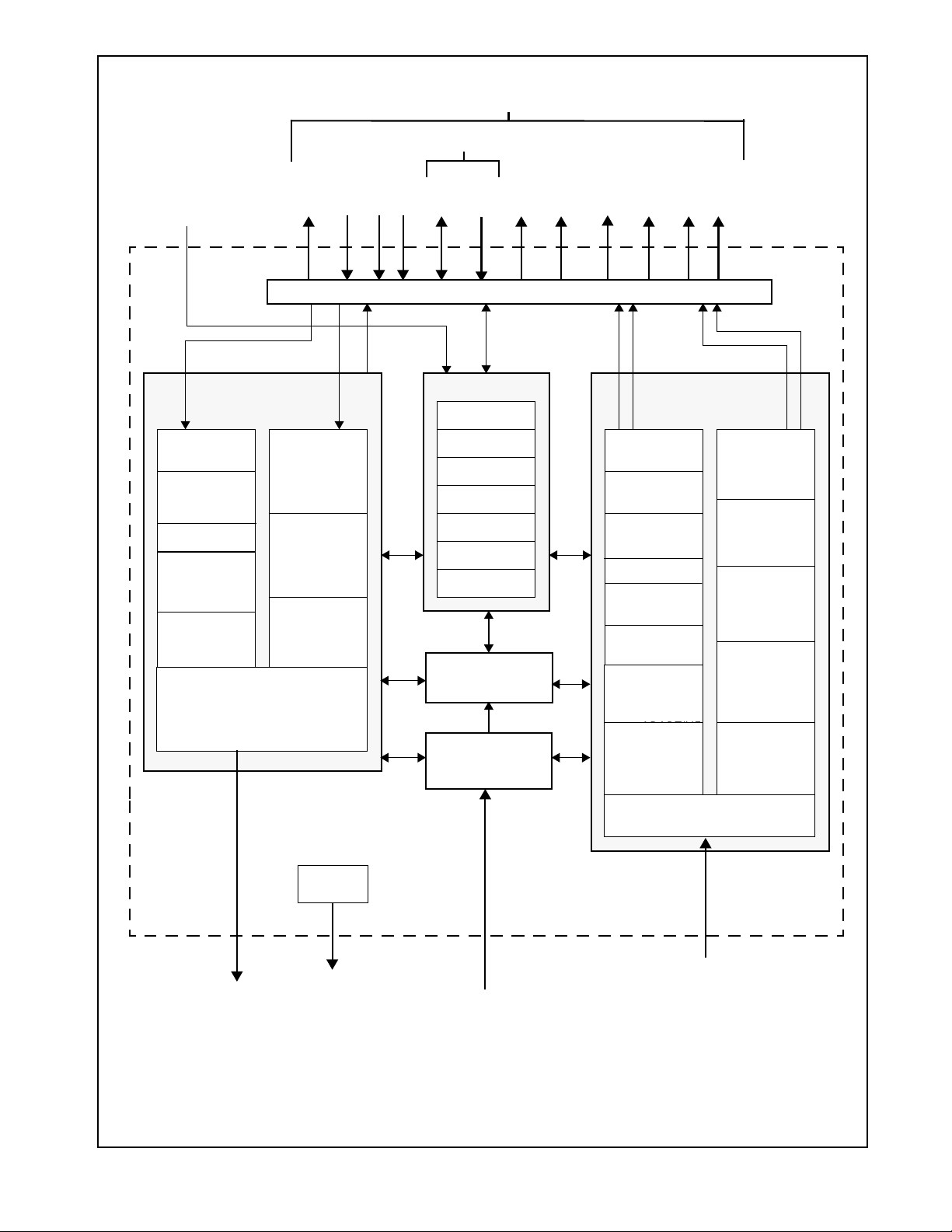
System Diagram
DP83846A
Clock
10/100 Mb/s
DsPHYTER
Status
LEDs
Typical DsPHYTER application
Ethernet MAC
MII
25 MHz
PHYTER® and TRI-STATE® are registered trademarks of National Semiconductor Corporation.
© 2000 National Semiconductor Corporation
Magnetics
RJ-45
10BASE-T
or
100BASE-TX
www.national.com
Page 2
MII
HARDWARE
CONFIGURATION
PINS
(AN_EN, AN0, AN1)
(PAUSE_EN)
(LED_CFG, PHYAD)
TX_DATA
TRANSMIT CHANNELS &
STATE MACHINES
100 Mb/s 10 Mb/s
4B/5B
ENCODER
PARALLEL TO
SERIAL
SCRAMBLER
NRZ TO NRZI
ENCODER
BINARY TO
MLT-3
ENCODER
10/100 COMMON
OUTPUT DRIVER
TX_CLK
TXD[3:0]
TX_DATA
NRZ TO
MANCHESTER
ENCODER
LINK PULSE
GENERATOR
TRANSMIT
FILTER
TX_ER
TX_CLK
SERIAL
MANAGEMENT
TX_EN
MDIO
MII INTERFACE/CONTROL
REGISTERS
PHY ADDRESS
AUTO
NEGOTIATION
BASIC MODE
CONTROL
PCS CONTROL
10BASE-T
100BASE-TX
AUTO-NEGOTIATION
STATE MACHINE
CLOCK
GENERATION
MDC
MII
COL
CRS
RX_CLK
RX_DV
RX_ER
RX_DATA
RECEIVE CHANNELS &
4B/5B
DECODER
CODE GROUP
ALIGNMENT
SERIAL TO
PARALLEL
DESCRAMBLER
NRZI TO NRZ
DECODER
CLOCK
RECOVERY
MLT-3 TO
BINARY
DECODER
ADAPTIVE
BLW
AND EQ
COMP
RXD[3:0]
STATE MACHINES
100 Mb/s 10 Mb/s
RX_CLK
RX_DATA
RX_CLK
MANCHESTER
TO NRZ
DECODER
CLOCK
RECOVERY
LINK PULSE
DETECTOR
RECEIVE
FILTER
SMART
SQUELCH
TD
LED
DRIVERS
LEDS
SYSTEM CLOCK
REFERENCE
Figure 1. Block Diagram of the 10/100 DSP based core.
2 www.national.com
10/100 COMMON
INPUT BUFFER
RD
Page 3

Table of Contents
1.0 Pin Descriptions . . . . . . . . . . . . . . . . . . . . . . . . . . . . . . .5
1.1 MII Interface . . . . . . . . . . . . . . . . . . . . . . . . . . . . . .5
1.2 10 Mb/s and 100 Mb/s PMD Interface . . . . . . . . . .6
1.3 Clock Interface . . . . . . . . . . . . . . . . . . . . . . . . . . . .7
1.4 Special Connections . . . . . . . . . . . . . . . . . . . . . . . 7
1.5 LED Interface . . . . . . . . . . . . . . . . . . . . . . . . . . . . .7
1.6 Strapping Options/Dual Purpose Pins . . . . . . . . . .8
1.7 Reset . . . . . . . . . . . . . . . . . . . . . . . . . . . . . . . . . . .9
1.8 Power and Ground Pins . . . . . . . . . . . . . . . . . . . . .9
1.9 Package Pin Assignments . . . . . . . . . . . . . . . . . . 10
2.0 Configuration . . . . . . . . . . . . . . . . . . . . . . . . . . . . . . .11
2.1 Auto-Negotiation . . . . . . . . . . . . . . . . . . . . . . . . . 11
2.2 PHY Address and LEDs . . . . . . . . . . . . . . . . . . .12
2.3 LED INTERFACES . . . . . . . . . . . . . . . . . . . . . . . 13
2.4 Half Duplex vs. Full Duplex . . . . . . . . . . . . . . . . .13
2.5 MII Isolate Mode . . . . . . . . . . . . . . . . . . . . . . . . .14
2.6 Loopback . . . . . . . . . . . . . . . . . . . . . . . . . . . . . . .14
2.7 BIST . . . . . . . . . . . . . . . . . . . . . . . . . . . . . . . . . . .14
3.0 Functional Description . . . . . . . . . . . . . . . . . . . . . . . .15
3.1 802.3u MII . . . . . . . . . . . . . . . . . . . . . . . . . . . . . .15
3.2 100BASE-TX TRANSMITTER . . . . . . . . . . . . . . .16
3.3 100BASE-TX RECEIVER . . . . . . . . . . . . . . . . . . 20
3.4 10BASE-T TRANSCEIVER MODULE . . . . . . . . .23
3.5 TPI Network Circuit . . . . . . . . . . . . . . . . . . . . . . .24
3.6 ESD Protection . . . . . . . . . . . . . . . . . . . . . . . . . .25
3.7 Crystal Oscillator Circuit . . . . . . . . . . . . . . . . . . .26
4.0 Reset Operation . . . . . . . . . . . . . . . . . . . . . . . . . . . . . .26
4.1 Hardware Reset . . . . . . . . . . . . . . . . . . . . . . . . . .26
4.2 Software Reset . . . . . . . . . . . . . . . . . . . . . . . . . .26
5.0 Register Block . . . . . . . . . . . . . . . . . . . . . . . . . . . . . . .27
5.1 Register Definition . . . . . . . . . . . . . . . . . . . . . . . .29
5.2 Extended Registers . . . . . . . . . . . . . . . . . . . . . . .37
6.0 Electrical Specifications . . . . . . . . . . . . . . . . . . . . . . .44
6.1 DC Electrical Specification . . . . . . . . . . . . . . . . . .44
6.2 PGM Clock Timing . . . . . . . . . . . . . . . . . . . . . . .46
6.3 MII Serial Management Timing . . . . . . . . . . . . . .46
6.4 100 Mb/s Timing . . . . . . . . . . . . . . . . . . . . . . . . .47
6.5 10 Mb/s Timing . . . . . . . . . . . . . . . . . . . . . . . . . .51
6.6 Reset Timing . . . . . . . . . . . . . . . . . . . . . . . . . . . .56
6.7 Loopback Timing . . . . . . . . . . . . . . . . . . . . . . . .57
6.8 Isolation Timing . . . . . . . . . . . . . . . . . . . . . . . . . .58
7.0 Package Information . . . . . . . . . . . . . . . . . . . . . . . . . .59
3 www.national.com
Page 4
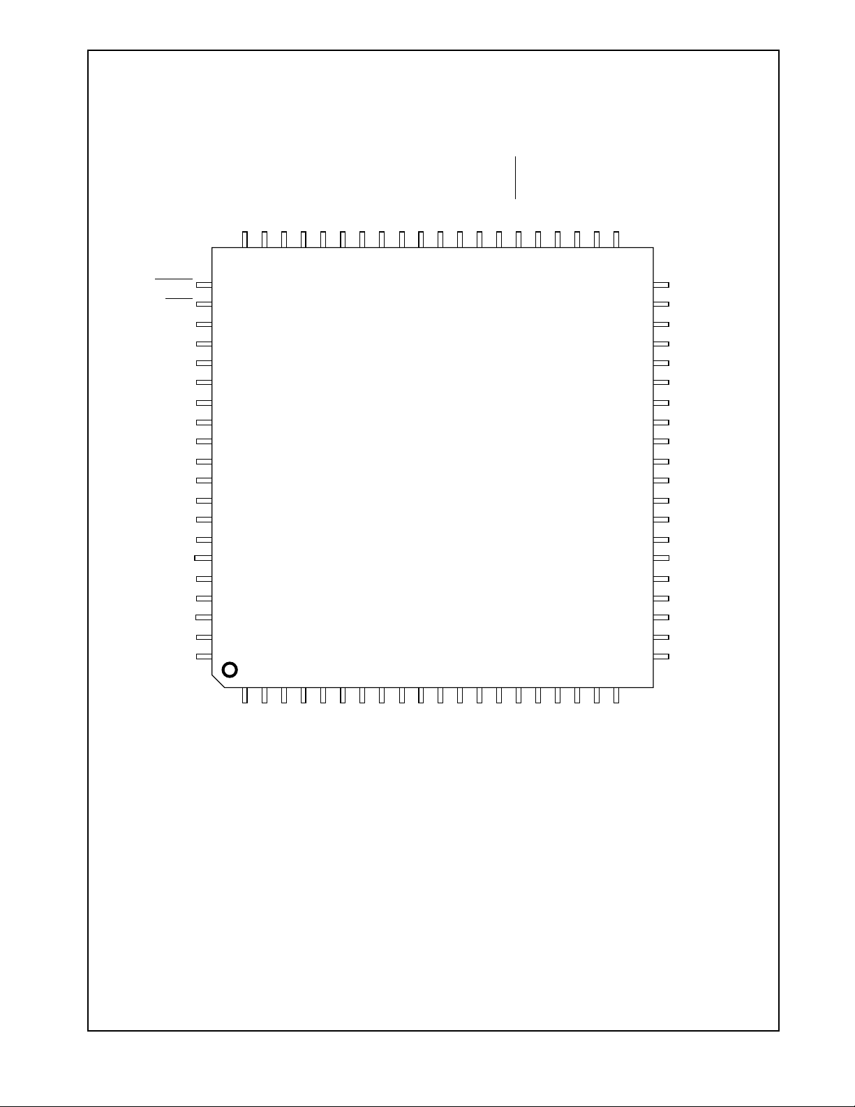
Connection Diagram
COL
60
CRS/LED_CFG
RESET
RESERVED
IO_GND
IO_VDD
RESERVED
RESERVED
RESERVED
RESERVED
CORE_VDD
CORE_GND
RESERVED
RESERVED
SUB_GND
RESERVED
RESERVED
SUB_GND
RESERVED
61
62
63
64
65
X2
66
X1
67
68
69
70
71
72
73
74
75
76
77
78
79
80
1
TXD_3
59
2
TXD_2
58
3
IO_VDD
57
4
IO_GND
TXD_1
56
55
5
6
TXD_0
IO_GND
TX_EN
TX_CLK
54
53
52
51
50
DP83846A
DSPHYTER
7
8
9
10
11
TX_ER
CORE_VDD
CORE_GND
49
48
12
13
RESERVED
RX_ER/PAUSE_EN
47
46
14
15
RX_CLK
45
16
RX_DV
44
17
IO_VDD
43
18
IO_GND
42
19
RXD_0
41
20
40
39
38
37
36
35
34
33
32
31
30
29
28
27
26
25
24
23
22
21
RXD_1
RXD_2
RXD_3
MDC
MDIO
IO_VDD
IO_GND
LED_DPLX/PHYAD0
LED_COL/PHYAD1
LED_GDLNK/PHYAD2
LED_TX/PHYAD3
LED_RX/PHYAD4
LED_SPEED
AN_EN
AN_1
AN_0
CORE_VDD
CORE_GND
RESERVED
RESERVED
ANA_GND
RESERVED
RD-
ANA_GND
RD+
ANA_VDD
ANA_GND
RBIAS
ANA_VDD
RESERVED
ANA_VDD
ANA_GND
RESERVED
Plastic Quad Flat Package JEDEC (LQFP)
Order Number DP83846AVHG
NS Package Number VHG80A
4 www.national.com
ANA_VDD
ANA_GND
TD+
TD-
ANA_GND
SUB_GND
RESERVED
Page 5

1.0 Pin Descriptions
The DP83846A pins are classified into the following interface categories (each interface is described in the sections
that follow):
— MII Interface
— 10/100 Mb/s PMD Interface
— Clock Interface
— Special Connect Pins
— LED Interface
— Strapping Options/Dual Function pins
— Reset
— Power and Ground pins
Note: Strapping pin option (BOLD) Please see Section 1.6
for strap definitions.
1.1 MII Interface
Signal Name Type Pin # Description
MDC I 37 MANAGEMENT DATA CLOCK: Synchronousclock to the
MDIO I/O, OD 36 MANAGEMENT DATA I/O: Bi-directional management in-
CRS/
LED_CFG O, S 61 CARRIER SENSE: Asserted high to indicate the presence
COL O 60 COLLISION DETECT: Asserted high to indicate detection
TX_CLK O 51 TRANSMIT CLOCK: 25 MHz Transmit clock outputs in
TXD[3]
TXD[2]
TXD[1]
TXD[0]]
TX_EN I 52 TRANSMIT ENABLE: Active high input indicates the pres-
TX_ER I 50 TRANSMIT ERROR: In 100MB/s mode, when this signal is
I 59,58,55,54TRANSMIT DATA: Transmit data MII input pinsthat accept
All DP83846A signal pins are I/O cells regardless of the
particular use. Below definitions define the functionality of
the I/O cells for each pin.
Type: I Inputs
Type: O Outputs
Type: I/O Input/Output
Type OD Open Drain
Type: PD,PU Internal Pulldown/Pullup
Type: S Strapping Pin (All strap pins except PHY-
AD[0:4] have internal pull-ups or pulldowns. If the default strap value is needed
to be changed then anexternal 5kΩ resistor
should be used. Please see Table 1.6 on
page 8 for details.)
MDIO management data input/output serialinterface which
may be asynchronous to transmit and receive clocks. The
maximum clockrate is 25 MHz with no minimum clock rate.
struction/data signal that may be sourced by the station
management entity or the PHY. This pin requires a 1.5 kΩ
pullup resistor.
of carrier due to receive or transmit activity in 10BASE-T or
100BASE-TX Half Duplex Modes, whilein full duplex mode
carrier sense is asserted to indicate the presence of carrier
due only to receive activity.
of a collision condition (simultaneous transmit and receive
activity) in 10 Mb/s and 100 Mb/s Half Duplex Modes.
While in 10BASE-T Half Duplex mode with Heartbeat enabled this pin are also asserted for a duration of approximately 1µs at the end of transmission to indicateheartbeat
(SQE test).
In Full Duplex Mode,for 10Mb/s or100Mb/s operation, this
signal is always logic 0. There is no heartbeat function during 10 Mb/s full duplex operation.
100BASE-TX mode or2.5 MHzin 10BASE-T modederived
from the 25 MHz reference clock.
nibble data synchronous to the TX_CLK (2.5 MHz in
10BASE-T Mode or 25 MHz in 100BASE-TX mode).
ence of valid nibble data on data inputs, TXD[3:0] for both
100 Mb/s or 10 Mb/s nibble mode.
high and thecorresponding TX_EN is active the HALT symbol is substituted for data.
In 10 Mb/s this input is ignored.
5 www.national.com
Page 6

Signal Name Type Pin # Description
RX_CLK O, PU 45 RECEIVE CLOCK: Provides the 25MHz recovered receive
RXD[3]
RXD[2]
RXD[1]
RXD[0]
RX_ER/PAUSE_EN S, O, PU 46 RECEIVE ERROR: Asserted high to indicate that an invalid
RX_DV O 44 RECEIVE DATAVALID: Asserted high toindicate thatvalid
O, PU/PD 38,39,40,41RECEIVE DATA: Nibble wide receivedata (synchronous to
clocks for 100BASE-TX mode and 2.5 MHz for 10BASE-T
nibble mode.
corresponding RX_CLK, 25 MHz for 100BASE-TX mode,
2.5 MHz for 10BASE-T nibble mode). Data is driven on the
falling edge of RX_CLK. RXD[2]has aninternal pulldown resistor. The remaining RXD pins have pullups.
symbol has been detected within a received packet in
100BASE-TX mode.
data is present on the corresponding RXD[3:0] for nibble
mode. Data is driven on the falling edge of the corresponding RX_CLK.
1.2 10 Mb/s and 100 Mb/s PMD Interface
Signal Name Type Pin # Description
TD+, TD- O 16, 17 Differential common driver transmit output. These differen-
RD-, RD+ I 10, 11 Differential receive input. These differential inputs can be
tial outputs are configurable to either 10BASE-T or
100BASE-TX signaling.
The DP83846A will automatically configure the common
driver outputs for the proper signal type as a result of either
forced configuration or Auto-Negotiation.
configured to accept either 100BASE-TX or 10BASE-T signaling.
The DP83846A will automatically configure the receive inputs to accept the proper signal type as a result of either
forced configuration or Auto-Negotiation.
6 www.national.com
Page 7

1.3 Clock Interface
Signal Name Type Pin # Description
X1 I 67 REFERENCE CLOCK INPUT 25 MHz: This pin is the pri-
X2 O 66 REFERENCE CLOCK OUTPUT 25 MHz: This pin is the
mary clock reference input for the DP83846A and must be
connected to a 25 MHz 0.005% (±50 ppm) clock source.
The DP83846A supports CMOS-level oscillator sources.
primary clock reference output.
1.4 Special Connections
Signal Name Type Pin # Description
RBIAS I 3 Bias Resistor Connection. A 9.31 kΩ1%resistor should be
RESERVED I/O 1, 5, 8, 20,
21, 22, 47,
63, 68, 69,
70, 71, 74,
75, 77, 78,
80
connected from RBIAS to ANA_GND.
RESERVED: These pins must be left unconnected.
1.5 LED Interface
Signal Name Type Pin # Description
LED_DPLX/PHYAD0 S, O 33 FULL DUPLEX LED STATUS: Indicates Full-Duplex sta-
LED_COL/PHYAD1 S, O 32 COLLISION LED STATUS: Indicates Collision activity in
LED_GDLNK/PHYAD2 S, O 31 GOOD LINK LED STATUS: Indicates Good Link Status for
LED_TX/PHYAD3 S, O 30 TRANSMIT LED STATUS: Indicates transmit activity. LED
LED_RX/PHYAD4 S, O 29 RECEIVE LED STATUS: Indicates receive activity. LED is
LED_SPEED O 28 SPEED LED STATUS: Indicates link speed; high for 100
tus.
Half Duplex mode.
10BASE-T and 100BASE-TX.
is on for activity, off for no activity.
on for activity, off for no activity.
Mb/s, low for 10 Mb/s.
7 www.national.com
Page 8
1.6 Strapping Options/Dual Purpose Pins
A5kΩ resistor should beused for pull-down or pull-up to changethe default strap option. Ifthe default option is required,
then there is no need for external pull-up or pull down resistors, since the internal pull-up or pull down resistors will set
the default value. Please note that the PHYAD[0:4] pins have no internal pull-ups or pull-downs and they must be
strapped. Since these pins may have alternate functions after reset is deasserted, they should not be connected directly
to Vcc or GND.
Signal Name Type Pin # Description
LED_DPLX/PHYAD0
LED_COL/PHYAD1
LED_GDLNK/PHYAD2
LED_TX/PHYAD3
LED_RX/PHYAD4
AN_EN
AN_1
AN_0
S, O 33
32
31
30
29
PHY ADDRESS [4:0]: The DP83846A provides five PHY
address pins,the state of which are latched into the PHYCTRL register at system Hardware-Reset.
The DP83846A supports PHY Address strapping values 0
(<00000>) through 31 (<11111>). PHY Address 0 puts
the part into the MII Isolate Mode. The MII isolate mode
must be selected by strapping Phy Address 0; changing to
Address 0 by register write will not put the Phy in the MII
isolate mode.
The status of these pins are latched into the PHY Control
Register during Hardware-Reset. (Please note these pins
have no internal pull-up orpull-down resistors andthey must
be strapped high or low using 5 kΩ resistors.)
S, O, PU 27, 26, 25 Auto-Negotiation Enable: When high enables Auto-Nego-
tiation with the capability set by ANO and AN1 pins. When
low, puts the part into Forced Mode with the capability set
by AN0 and AN1 pins.
AN0 / AN1: These input pins control the forced or advertised operating mode of the DP83846Aaccording tothe following table. The value on these pins is set by connecting
the input pins to GND (0) or V
These pins should NEVER be connected directly to
GND or V
CC.
(1) through 5 kΩ resistors.
CC
The value set at this input is latched into the DP83846A at
Hardware-Reset.
The float/pull-down status of these pins are latched into the
Basic Mode Control Register and the Auto_Negotiation Advertisement Register during Hardware-Reset. After reset is
deasserted, these pins may switch to outputs so if pull-ups
or pull-downs are implemented, they should be pulled
through a 5kΩ resistor.
The default is 111 since these pins have pull-ups.
AN_EN AN1 AN0 Forced Mode
0 0 0 10BASE-T, Half-Duplex
0 0 1 10BASE-T, Full-Duplex
0 1 0 100BASE-TX, Half-Duplex
0 1 1 100BASE-TX, Full-Duplex
AN_EN AN1 AN0 Advertised Mode
1 0 0 10BASE-T, Half/Full-Duplex
1 0 1 100BASE-TX,Half/Full-Duplex
1 1 0 10BASE-T Half-Duplex
100BASE-TX, Half-Duplex
1 1 1 10BASE-T, Half/Full-Duplex
100BASE-TX,Half/Full-Duplex
8 www.national.com
Page 9

Signal Name Type Pin # Description
RX_ER/PAUSE_EN S, O, PU 46 PAUSE ENABLE: This strapping option allows advertise-
CRS/
LED_CFG S, O
PU
61 LED CONFIGURATION: This strapping option defines the
,
ment of whether or not the DTE(MAC) has implemented
both the optional MAC control sublayer andthe pausefunction as specified in clause 31 and annex 31B of the IEEE
802.3x specification (Full Duplex Flow Control).
When left floating the Auto-Negotiation Advertisement Reg-
ister will be set to 0, indicatingthat Full Duplex Flow Control
is not supported.
When tied low through a 5 kΩ, the Auto-Negotiation Advertisement Register will be set to 1,indicating that Full Duplex
Flow Control is supported.
The float/pull-down status ofthispin is latchedinto theAutoNegotiation Advertisement Register during Hardware-Reset.
polarity and function of the FDPLX LED pin.
See Section 2.3 for further descriptions of this strappingop-
tion.
1.7 Reset
Signal Name Type Pin # Description
RESET I 62 RESET: Active Low input that initializes or re-initializes the
DP83846A. Asserting this pin low for at least 160 µs will
force a reset processto occurwhich willresult inall internal
registers re-initializing to theirdefault states as specified for
each bit in the Register Block section and all strapping options are re-initialized.
1.8 Power and Ground Pins
Signal Name Pin # Description
TTL/CMOS INPUT/OUTPUT SUPPLY
IO_VDD 35, 43, 57, 65 I/O Supply
IO_GND 34, 42, 53, 56, 64 I/O Ground
INTERNAL SUPPLY PAIRS
CORE_VDD 24, 49, 72 Digital Core Supply
CORE_GND 23, 48, 73 Digital Core Ground
ANALOG SUPPLY PINS
ANA_VDD 4, 7, 12, 14 Analog Supply
ANA_GND 2, 6, 9, 13, 15, 18, Analog Ground
SUBSTRATE GROUND
SUB_GND 19, 76, 79 Bandgap Substrate connection
9 www.national.com
Page 10

1.9 Package Pin Assignments
Pin # Pin Name
1 RESERVED
2 ANA_GND
3 RBIAS
4 ANA_VDD
5 RESERVED
6 ANA_GND
7 ANA_VDD
8 RESERVED
9 ANA_GND
10 RD11 RD+
12 ANA_VDD
13 ANA_GND
14 ANA_VDD
15 ANA_GND
16 TD+
17 TD18 ANA_GND
19 SUB_GND
20 RESERVED
21 RESERVED
22 RESERVED
23 CORE_GND
24 CORE_VDD
25 AN_0
26 AN_1
27 AN_EN
28 LED_SPEED
29 LED_RX /PHYAD4
30 LED_TX /PHYAD3
31 LED_GDLNK/PHYAD2
32 LED_COL /PHYAD1
33 LED_FDPLX /PHYAD0
34 IO_GND
35 IO_VDD
36 MDIO
37 MDC
38 RXD_3
39 RXD_2
40 RXD_1
Pin # Pin Name
41 RXD_0
42 IO_GND
43 IO_VDD
44 RX_DV
45 RX_CLK
46 RX_ER/
PAUSE_EN
47 RESERVED
48 CORE_GND
49 CORE_VDD
50 TX_ER
51 TX_CLK
52 TX_EN
53 IO_GND
54 TXD_0
55 TXD_1
56 IO_GND
57 IO_VDD
58 TXD_2
59 TXD_3
60 COL
61 CRS/
LED_CFG
62 RESET
63 RESERVED
64 IO_GND
65 IO_VDD
66 X2
67 X1
68 RESERVED
69 RESERVED
70 RESERVED
71 RESERVED
72 CORE_VDD
73 CORE_GND
74 RESERVED
75 RESERVED
76 SUB_GND
77 RESERVED
78 RESERVED
79 SUB_GND
80 RESERVED
10 www.national.com
Page 11

2.0 Configuration
This section includes information on the various configuration options available with the DP83846A. The configuration options described below include:
— Device Configuration
— Auto-Negotiation
— PHY Address and LEDs
— Half Duplex vs. Full Duplex
— Isolate mode
— Loopback mode
— BIST
2.1 Auto-Negotiation
The Auto-Negotiation function provides a mechanism for
exchanging configuration information between two ends of
a link segment and automatically selecting the highest performance mode of operation supported by both devices.
Fast Link Pulse (FLP) Bursts provide the signalling used to
communicate Auto-Negotiation abilities between two
devices at each end of a link segment. For further detail
regarding Auto-Negotiation, refer to Clause 28 of the IEEE
802.3u specification. The DP83846A supports four different Ethernet protocols (10 Mb/s Half Duplex, 10 Mb/s Full
Duplex, 100 Mb/s Half Duplex, and 100 Mb/s Full Duplex),
so the inclusion of Auto-Negotiation ensures that the highest performance protocol will be selected based on the
advertised ability of the Link Partner. The Auto-Negotiation
function within the DP83846A can be controlled either by
internal register access or by the use of the AN_EN, AN1
and AN0 pins..
2.1.1 Auto-Negotiation Pin Control
The state of AN_EN, AN0 and AN1 determines whether
the DP83846A is forced intoa specific mode or Auto-Negotiation will advertise a specific ability (or set of abilities) as
given in Table 1. These pins allow configuration options to
be selected without requiring internal register access.
The state of AN_EN, AN0 and AN1, upon power-up/reset,
determines the state of bits [8:5] of the ANAR register.
The Auto-Negotiation function selected at power-up or
reset can be changed at any time by writing to the Basic
Mode Control Register (BMCR) at address 00h.
Table 1. Auto-Negotiation Modes
AN_EN AN1 AN0 Forced Mode
0 0 0 10BASE-T, Half-Duplex
0 0 1 10BASE-T, Full-Duplex
0 1 0 100BASE-TX, Half-Duplex
0 1 1 100BASE-TX, Full-Duplex
AN_EN AN1 AN0 Advertised Mode
1 0 0 10BASE-T, Half/Full-Duplex
1 0 1 100BASE-TX, Half/Full-Duplex
1 1 0 10BASE-T Half-Duplex
100BASE-TX, Half-Duplex
1 1 1 10BASE-T, Half/Full-Duplex
100BASE-TX, Half/Full-Duplex
2.1.2 Auto-Negotiation Register Control
When Auto-Negotiation is enabled, the DP83846A transmits the abilities programmed into the Auto-Negotiation
Advertisement register (ANAR) at address 04h via FLP
Bursts. Any combination of 10 Mb/s, 100 Mb/s, HalfDuplex, and Full Duplex modes may be selected. The
BMCR provides software with a mechanism to control the
operation of the DP83846A. The AN0 and AN1 pins do not
affect the contents of the BMCR and cannot be used by
software to obtainstatus of the mode selected.Bits 1 & 2 of
the PHYSTS register are only valid if Auto-Negotiation is
disabled or after Auto-Negotiation is complete. The AutoNegotiation protocol comparesthe contents of the ANLPAR
and ANAR registers and uses the results to automatically
configure to the highest performance protocol between the
local and far-end port. The results of Auto-Negotiation
(Auto-Neg Complete, Duplex Status and Speed) may be
accessed in the PHYSTS register.
Auto-Negotiation Priority Resolution:
— (1) 100BASE-TX Full Duplex (Highest Priority)
— (2) 100BASE-TX Half Duplex
— (3) 10BASE-T Full Duplex
— (4) 10BASE-T Half Duplex (Lowest Priority)
The Basic Mode Control Register (BMCR) at address 00h
provides control for enabling, disabling, and restarting the
Auto-Negotiation process. When Auto-Negotiation is disabled the Speed Selection bit inthe BMCR controls switching between 10 Mb/s or 100 Mb/s operation, and the
Duplex Mode bit controls switching between full duplex
operation and half duplex operation. The Speed Selection
and Duplex Modebits have no effect on the mode of operation when the Auto-Negotiation Enable bit is set.
The Basic Mode Status Register (BMSR) indicates the set
of available abilities for technology types, Auto-Negotiation
ability, and Extended Register Capability. These bits are
permanently set to indicate the full functionality of the
DP83846A (only the 100BASE-T4 bit is not set since the
DP83846A does not support that function).
11 www.national.com
Page 12

The BMSR also provides status on:
— Whether Auto-Negotiation is complete
— Whether the Link Partner is advertising that a remote
fault has occurred
— Whether valid link has been established
— Support for Management FramePreamble suppression
The Auto-Negotiation Advertisement Register (ANAR) indi-
cates the Auto-Negotiation abilities to be advertised by the
DP83846A. Allavailable abilities are transmitted by default,
but any ability can be suppressed by writing to the ANAR.
Updating the ANAR to suppress an ability is one way for a
management agent to change (force)the technologythat is
used.
The Auto-Negotiation Link Partner Ability Register
(ANLPAR) at address 05h is used to receive the base link
code word as well as all next page code words during the
negotiation. Furthermore, the ANLPAR will be updated to
either 0081h or 0021h for parallel detection to either 100
Mb/s or 10 Mb/s respectively.
The Auto-Negotiation Expansion Register (ANER) indicates additional Auto-Negotiation status. The ANER provides status on:
— Whether a Parallel Detect Fault has occurred
— Whether the Link Partner supports the Next Page func-
tion
— Whether the DP83846A supportsthe NextPage function
— Whether the current page beingexchanged by Auto-Ne-
gotiation has been received
— Whether the Link Partner supports Auto-Negotiation
2.1.3 Auto-Negotiation Parallel Detection
The DP83846A supports the Parallel Detection function as
defined in the IEEE 802.3u specification. Parallel Detection
requires both the 10 Mb/s and 100 Mb/s receivers to monitor the receive signal and report link status to the AutoNegotiation function. Auto-Negotiation uses this information to configure the correct technology inthe event that the
Link Partner does not support Auto-Negotiation but is
transmitting link signals that the 100BASE-TX or 10BASET PMAs recognize as valid link signals.
If the DP83846A completes Auto-Negotiation as a result of
Parallel Detection, bits 5 and 7 within the ANLPAR register
will be set to reflect the mode of operation present in the
Link Partner. Note that bits 4:0 of the ANLPAR will also be
set to 00001 based on a successful parallel detection to
indicate a valid 802.3 selector field. Software may determine that negotiation completed via Parallel Detection by
reading azero inthe Link Partner Auto-NegotiationAble bit
once the Auto-Negotiation Complete bit is set. If configured
for parallel detect mode and any condition other than a single good link occurs then the paralleldetect fault bitwill set.
2.1.4 Auto-Negotiation Restart
Once Auto-Negotiation has completed, it may be restarted
at any timeby setting bit 9 (Restart Auto-Negotiation) of the
BMCR to one. If themode configured by a successfulAutoNegotiation loses a valid link, then the Auto-Negotiation
process will resume and attempt to determine the configuration for the link. This function ensures that a valid configuration is maintained if the cable becomes disconnected.
A renegotiation request from any entity, such as a management agent, will cause the DP83846A to halt any transmit
data and link pulse activity until the break_link_timer
expires (~1500 ms). Consequently, the Link Partner will go
into link fail and normal Auto-Negotiation resumes. The
DP83846A will resume Auto-Negotiation after the
break_link_timer has expired by issuing FLP (Fast Link
Pulse) bursts.
2.1.5 Enabling Auto-Negotiation via Software
It is important to note that if the DP83846A has been initialized upon power-up as a non-auto-negotiating device
(forced technology), and it is then required that Auto-Negotiation or re-Auto-Negotiation be initiated via software,
bit 12 (Auto-Negotiation Enable) of the Basic Mode Control
Register must first be cleared and then set for any AutoNegotiation function to take effect.
2.1.6 Auto-Negotiation Complete Time
Parallel detection and Auto-Negotiation take approximately
2-3 seconds to complete. In addition, Auto-Negotiation with
next page should take approximately 2-3 seconds to complete, depending on the number of next pages sent.
Refer to Clause 28 of the IEEE 802.3u standard for a full
description of the individual timers related to Auto-Negotiation.
2.2 PHY Address and LEDs
The 5 PHY address inputs pins are shared with the LED
pins as shown below.
Table 2. PHY Address Mapping
Pin # PHYAD Function LED Function
33 PHYAD0 Duplex
32 PHYAD1 COL
31 PHYAD2 Good Link
30 PHYAD3 TX Activity
29 PHYAD4 RX Activity
28 n/a Speed
The DP83846A can be set to respond to any of 32 possible
PHY addresses. Each DP83846A or port sharing an MDIO
bus in a system must have a unique physical address.
Refer to Section 3.1.4, PHY Address Sensing section for
more details.
The state of each of the PHYAD inputs latched into the
PHYCTRL register bits [4:0] at system power-up/reset
depends on whether a pull-up or pull-down resistor has
been installed for each pin. For further detail relating to the
latch-in timing requirements of the PHY Address pins, as
well as the other hardware configuration pins, refer to the
Reset summary in Section 4.0.
Since the PHYAD strap options share the LED output pins,
the external components required for strapping and LED
usage must be considered in order to avoid contention.
Specifically, when the LED outputs are used to drive LEDs
directly, the active state of each output driver is dependent
on the logic level sampled by the corresponding PHYAD
input upon power-up/reset. For example, if a given PHYAD
input is resistively pulled low then the corresponding output
will be configured as an active high driver. Conversely, if a
given PHYAD input is resistivelypulled high, then the corresponding output will be configured as an active low driver.
12 www.national.com
Page 13
Refer to Figure 2 for an example of a PHYAD connection to
external components. In this example, the PHYAD strapping results in address 00011 (03h).
The adaptive nature of the LED outputs helps to simplify
potential implementation issues of these dual purpose
pins.
LED_RX
PHYAD4= 0
1kΩ
10kΩ
Figure 2. PHYAD Strapping and LED Loading Example
LED_TX
1kΩ
10kΩ
LED_GDLNK
10kΩ
2.3 LED INTERFACES
The DP83846A has 6 Light Emitting Diode (LED) outputs
to indicate the status of Link, Transmit, Receive, Collision,
Speed, and Full/Half Duplex operation. The LED_CFG
strap option is used to configure the LED_FDPLX output
for use as an LED driver or more general purpose control
pin. See the table below:
Table 3. LED Mode Select
LED_CFG Mode Description
1 LED polarity adjusted
0 Duplex active-high
The LED_FDPLX pin indicates the Half or Full Duplex configuration of the port in both 10 Mb/s and 100 Mb/s operation. Since this pin is also used as the PHY address strap
option, thepolarity of this indicator may be adjusted so that
in the “active” (FULL DUPLEX selected) state it drives
against the pullup/pulldown strap. In this configuration it is
suitable for use as an LED. When LED_CFG is high this
mode is selected and DsPHYTER automatically adjusts
the polarity of the output. If LED_CFG is low, the output
drives high to indicate the “active” state. In this configuration the output is suitable for use as a control pin. The
LED_SPEED pin indicates 10 or 100 Mb/s data rate of the
port. The standard CMOS driver goes high when operating
in 100 Mb/s operation. Since this pin is not utilized as a
strap option, it is not affected by polarity adjustment.
The LED_GDLNK pin indicates the link status of the port.
Since this pin is also used as the PHY address strap
option, the polarity of this indicator is adjusted to be the
inverse of the strap value.
LED_COL
PHYAD2 = 0PHYAD3 = 0
1kΩ
In 100BASE-T mode, link is established as a result of input
receive amplitude compliant with TP-PMD specifications
which will result in internal generation of signal detect.
10 Mb/s Link is establishedas a result of the reception ofat
least seven consecutive normal Link Pulses or the reception of a valid 10BASE-T packet. This will cause the assertion of GD_LINK. GD_LINK will deassert in accordance
with the Link Loss Timer as specified in IEEE 802.3.
The Collision LED indicates the presence of collision activity for 10 Mb/s or 100 Mb/s Half Duplex operation. This bit
has no meaning in Full Duplex operation and will be deasserted when the port is operating in Full Duplex. Since this
pin is also used as the PHY addressstrap option, thepolarity of this indicator is adjusted to be the inverse of the strap
value. In 10 Mb/s half duplex mode, the collision LED is
based on the COL signal. When in this mode, the user
should disable the Heartbeat (SQE) to avoid asserting the
COL LED during transmission. See Section 3.4.2 for more
information about the Heartbeat signal.
The LED_RX and LED_TX pins indicate the presence of
transmit and/or receive activity. Since these pins are also
used in PHY address strap options, the polarity is adjusted
to be the inverse of the respective strap values.
PHYAD1 = 1
1kΩ
10kΩ
LED_FDPLX
PHYAD0 = 1
1kΩ
10kΩ
VCC
2.4 Half Duplex vs. Full Duplex
The DP83846A supports both half and fullduplex operation
at both 10 Mb/s and 100 Mb/s speeds. Half-duplex is the
standard, traditional mode of operation which relies on the
CSMA/CD protocol to handle collisions and network
access. In Half-Duplex mode, CRS responds to both transmit and receive activity in order to maintain compliance
with IEEE 802.3 specification.
Since the DP83846A is designed to support simultaneous
transmit and receive activity it is capable of supporting fullduplex switched applicationswith athroughput ofup to200
13 www.national.com
Page 14

Mb/s per port when operating in 100BASE-TX mode.
Because the CSMA/CD protocol does not apply to fullduplex operation, the DP83846A disables its own internal
collision sensing and reporting functions and modifies the
behavior of Carrier Sense (CRS) such that it indicates only
receive activity. This allows a full-duplex capable MAC to
operate properly.
All modes of operation (100BASE-TX and 10BASE-T) can
run either half-duplex or full-duplex. Additionally, other than
CRS and Collision reporting, all remaining MII signaling
remains the same regardless of the selected duplex mode.
It is important to understand that while Auto-Negotiation
with the use of Fast Link Pulse code words can interpret
and configure to full-duplex operation, parallel detection
can not recognize the difference between full and halfduplex from a fixed 10 Mb/s or 100 Mb/s link partner over
twisted pair. As specified in 802.3u, if a far-end link partner
is transmitting forced full duplex 100BASE-TX for example,
the parallel detection state machine in the receiving station
would be unable to detect the full duplex capability of the
far-end link partner and would negotiate to a half duplex
100BASE-TX configuration (same scenario for 10 Mb/s).
2.5 MII Isolate Mode
The DP83846A can be put into MII Isolate mode by writing
to bit 10 of the BMCR register. In addition, the MII isolate
mode can be selected by strapping in Physical Address 0.
It should be noted that selecting Physical Address 0 via an
MDIO write to PHYCTRL will not put the device in the MII
isolate mode.
When in the MII isolate mode, the DP83846A does not
respond to packet data present at TXD[3:0], TX_EN, and
TX_ER inputs and presents a high impedance on the
TX_CLK, RX_CLK, RX_DV, RX_ER, RXD[3:0], COL, and
CRS outputs. The DP83846A will continue to respond toall
management transactions.
While in Isolate mode, the TD± outputs will not transmit
packet data but will continue to source 100BASE-TX
scrambled idles or 10BASE-T normal link pulses.
2.6 Loopback
The DP83846A includes a LoopbackTest mode for facilitating system diagnostics. The Loopback mode is selected
through bit 14 (Loopback) of the Basic Mode Control Register (BMCR). Writing 1 to this bit enables MII transmit data
to be routed to the MII receive outputs. Loopback status
may be checked in bit 3 of the PHY Status Register
(PHYSTS). While in Loopback mode the data will not be
transmitted onto the media in 100 Mb/s mode. To ensure
that the desired operating mode is maintained, Auto-Negotiation should be disabled before selecting the Loopback
mode.
During 10BASE-T operation, in order to be standard compliant, the loopback mode loopsMII transmitdata to the MII
receive data, however, Link Pulses are not looped back.
When selecting 10 Mb/s Loopback, Good Link must be
forced via the FORCE_LINK_10 bit in the 10BTSCR. Also
in the 10 Mb/s Loopback mode, the CD should be disabled
(bit 15 in the CDCTRL) to prevent transmission of the
Loopback data onto the network.
In 100BASE-TX Loopback mode the data is routed through
the PCS and PMA layers into the PMD sublayer before it is
looped back. In addition to serving as a board diagnostic,
this mode serves as a functional verification of the device.
2.7 BIST
The DsPHYTER incorporates an internal Built-in Self Test
(BIST) circuit to accommodate in-circuit testing or diagnostics. The BIST circuit can be utilized to test the integrity of
the transmit and receive data paths. BIST testing can be
performed with the part in the internal loopback mode or
externally looped back using a loopback cable fixture.
The BIST is implemented with independent transmit and
receive paths, with the transmit block generating a continuous stream of a pseudo random sequence. The user can
select a 9 bit or 15 bit pseudo random sequence from the
PSR_15 bit in the PHY Control Register (PHYCTRL). The
looped back data is compared to the data generated bythe
BIST Linear Feedback Shift Register (LFSR, which generates a pseudo random sequence) to determine the BIST
pass/fail status.
The pass/fail status of the BIST is stored in the BIST status
bit in the PHYCTRL register. The status bit defaults to 0
(BIST fail) and will transition on a successful comparison. If
an error (mis-compare) occurs, the status bit is latched and
is cleared upon a subsequent write to the Start/Stop bit.
14 www.national.com
Page 15
3.0 Functional Description
3.1 802.3u MII
The DP83846A incorporates the Media Independent Interface (MII) as specified in Clause 22 of the IEEE 802.3u
standard. This interface may be used to connect PHY
devices to a MAC in 10/100 Mb/s systems. This section
describes both the serial MII management interface as well
as the nibble wide MII data interface.
The serial management interface of the MII allows for the
configuration and control of multiple PHY devices, gathering of status, error information, and the determination of
the type and capabilities of the attached PHY(s).
The nibble wide MII data interface consistsof areceive bus
and a transmit bus each with control signals to facilitate
data transfer between the PHY and the upper layer (MAC).
3.1.1 Serial Management Register Access
The serial management MII specification defines a set of
thirty-two 16-bit status and control registers that are accessible through the management interface pins MDC and
MDIO. The DP83846A implements all the required MII registers as well as several optional registers. These registers
are fully described in Section 5. A description of the serial
management access protocol follows.
3.1.2 Serial Management Access Protocol
The serial control interface consists of two pins, Management Data Clock (MDC) and Management Data Input/Output (MDIO). MDC has a maximum clock rate of 25 MHz
and no minimum rate. The MDIO line is bi-directional and
may be shared by up to 32 devices. The MDIO frame format is shown below in Table 4.
The MDIO pin requires a pull-up resistor (1.5 kΩ) which,
during IDLE and turnaround, will pull MDIO high. In order
to initialize the MDIO interface, the station management
entity sends a sequence of 32 contiguous logic ones on
MDIO to provide the DP83846A with a sequence that can
be used to establish synchronization. This preamble may
be generated either by driving MDIO high for 32 consecutive MDC clock cycles, orby simply allowing the MDIO pullup resistor to pull the MDIO pin high during which time 32
MDC clock cycles are provided. In addition 32 MDC clock
cycles should be used to re-sync the device if an invalid
start, opcode, or turnaround bit is detected.
The DP83846A waits until it has received this preamble
sequence before responding to any other transaction.
Once the DP83846A serial management port has been initialized no further preamble sequencing is required until
after a power-on/reset, invalid Start, invalid Opcode, or
invalid turnaround bit has occurred.
The Start code is indicated bya <01> pattern. Thisassures
the MDIO line transitions from the default idle line state.
Turnaround is defined as an idle bit time inserted between
the Register Address field and the Data field. To avoid contention during a read transaction, no device shall actively
drive the MDIOsignal during the first bitof Turnaround.The
addressed DP83846A drives the MDIO with a zero for the
second bit of turnaround and follows this with the required
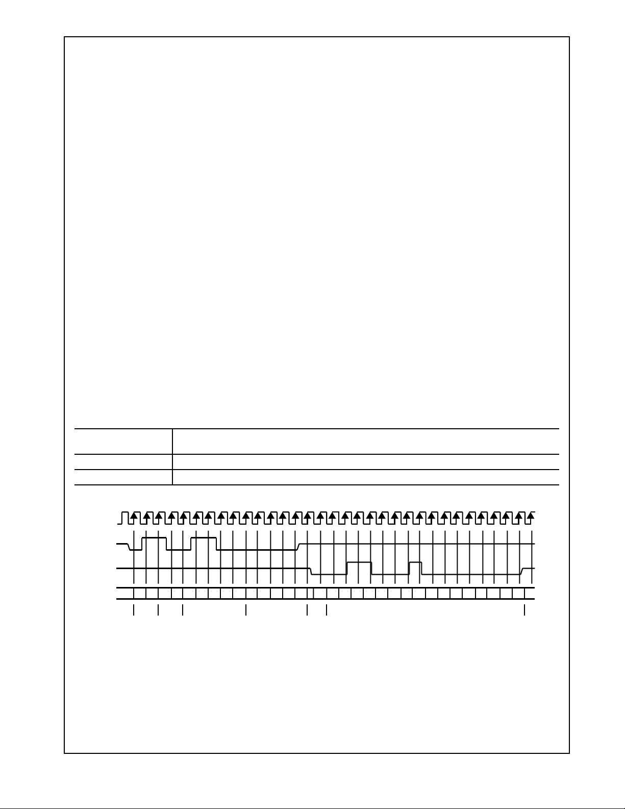
data. Figure 3 shows the timing relationship between MDC
and the MDIO as driven/received by the Station (STA) and
the DP83846A (PHY) for a typical register read access.
Table 4. Typical MDIO Frame Format
MII Management
<idle><start><op code><device addr><reg addr><turnaround><data><idle>
Serial Protocol
Read Operation <idle><01><10><AAAAA><RRRRR><Z0><xxxx xxxx xxxx xxxx><idle>
Write Operation <idle><01><01><AAAAA><RRRRR><10><xxxx xxxx xxxx xxxx><idle>
MDC
MDIO
(STA)
MDIO
(PHY)
Z
Z
00011 110000000
Idle Start
Opcode
(Read)
PHY Address
(PHYAD = 0Ch)
Register Address
(00h = BMCR)
Z
Z
Z
0 0 011000100000000
TA
Register Data
Figure 3. Typical MDC/MDIO Read Operation
For write transactions, the station management entity
writes data to the addressed DP83846A thus eliminating
the requirement for MDIO Turnaround. The Turnaround
time is filled by the management entity by inserting <10>.
Figure 4 shows the timing relationship for a typical MII register write access.
3.1.3 Serial Management Preamble Suppression
The DP83846A supports a Preamble Suppression mode
as indicated by a one in bit 6 of the Basic Mode Status
Register (BMSR, address 01h.) If the station management
entity (i.e. MAC or other management controller) determines that all PHYs in the system support Preamble Suppression by returning a one in this bit, then the station
Z
Z
Idle
15 www.national.com
Page 16

MDC
MDIO
(STA)
Z
00011110000000
Idle Start
Opcode
(Write)
PHY Address
(PHYAD = 0Ch)
Register Address
(00h = BMCR)
Figure 4. Typical MDC/MDIO Write Operation
management entity need not generate preamble for each
management transaction.
The DP83846A requires a single initialization sequence of
32 bits of preamble following hardware/software reset. This
requirement is generally met by the mandatory pull-up
resistor on MDIO in conjunction with a continuous MDC, or
the management access made to determine whether Preamble Suppression is supported.
While the DP83846A requires an initial preamblesequence
of 32 bits for management initialization, it does not require
a full 32-bit sequence between each subsequent transaction. A
transactions is required
minimum of one idle bit between management
as specified in IEEE 802.3u.
3.1.4 PHY Address Sensing
The DP83846A provides five PHY address pins, the information is latched into the PHYCTRL register (address 19h,
bits [4:0]) at device power-up/Hardware reset.
The DP83846A supports PHY Address strapping values 0
(<00000>) through 31 (<11111>). Strapping PHY Address
0 puts the part into Isolate Mode. It should also be noted
that selecting PHY Address 0 via an MDIO write to PHYCTRL will not put the device in Isolate Mode; Address 0 must
be strapped in.
3.1.5 Nibble-wide MII Data Interface
Clause 22 of the IEEE 802.3u specification defines the
Media Independent Interface. This interface includes a
dedicated receive bus and a dedicated transmit bus. These
two data buses, along with various control and indicate signals, allow for the simultaneous exchange of data between
the DP83846A and the upper layer agent (MAC).
The receive interface consists of a nibble wide data bus
RXD[3:0], a receive error signal RX_ER, a receive data
valid flag RX_DV,and a receive clock RX_CLK for synchronous transfer of the data. The receive clock can operate at
either 2.5 MHz to support 10 Mb/s operation modes or at
25 MHz to support 100 Mb/s operational modes.
The transmit interface consists of a nibble wide data bus
TXD[3:0], a transmit enable control signal TX_EN, and a
transmit clock TX_CLK which runs at either 2.5 MHz or 25
MHz.
Additionally, the MII includes the carrier sense signal CRS,
as well as a collision detect signal COL. The CRS signal
asserts to indicate the reception of data from the network
or as a function of transmit data in Half Duplex mode. The
COL signal asserts asan indication of a collision which can
occur during half-duplex operation when both a transmit
and receive operation occur simultaneously.
ZZ
0 0 0 000 00000000
1000
TA
Register Data
3.1.6 Collision Detect
For Half Duplex, a 10BASE-T or 100BASE-TX collision is
detected when the receive and transmit channels are
active simultaneously. Collisions are reported by the COL
signal on the MII.
If the DP83846A is transmitting in 10 Mb/s mode when a
collision is detected, the collision is not reported until seven
bits have been received while in the collision state. This
prevents a collision being reported incorrectly due to noise
on the network. The COL signal remains set for the duration of the collision.
If a collision occurs during areceive operation, it is immediately reported by the COL signal.
When heartbeat is enabled (only applicable to 10 Mb/s
operation), approximately 1µs after the transmission of
each packet, a Signal Quality Error (SQE) signal of approximately 10 bit times is generated (internally) to indicate
successful transmission. SQE is reported asa pulseon the
COL signal of the MII.
3.1.7 Carrier Sense
Carrier Sense(CRS) may be asserted due to receive activity, once valid data is detected via the squelch function during 10 Mb/s operation. During 100 Mb/s operation CRS is
asserted when a valid link (SD) and two non-contiguous
zeros are detected on the line.
For 10 or 100 Mb/s Half Duplex operation, CRS is asserted
during either packet transmission or reception.
For 10 or 100 Mb/s Full Duplex operation, CRS is asserted
only due to receive activity.
CRS is deasserted following an end of packet.
3.2 100BASE-TX TRANSMITTER
The 100BASE-TX transmitter consists of several functional
blocks which convert synchronous 4-bit nibble data,as provided by theMII, to a scrambled MLT-3125 Mb/s serial data
stream. Because the 100BASE-TX TP-PMD is integrated,
the differential output pins, TD±, can be directly routed to
the magnetics.
The block diagram in Figure 5 provides an overview of
each functional block within the 100BASE-TX transmit section.
The Transmitter section consists of the following functional
blocks:
— Code-groupEncoderandInjectionblock(bypassoption)
— Scrambler block (bypass option)
— NRZ to NRZI encoder block
— Binary to MLT-3 converter / Common Driver
Z
Idle
16 www.national.com
Page 17

The bypass option for the functional blocks within the
100BASE-TX transmitter provides flexibility for applications
where data conversion is not always required. The
DP83846A implements the 100BASE-TX transmit state
machine diagram as specified in the IEEE 802.3u Standard, Clause 24.
FROM PGM
BP_4B5B
BP_SCR
TX_CLK
DIV BY 5
TXD[3:0]/
TX_ER
4B5B CODE-
GROUP ENCODER
& INJECTOR
MUX
5B PARALLEL
TO SERIAL
SCRAMBLER
MUX
100BASE-TX
LOOPBACK
Figure 5. 100BASE-TX Transmit Block Diagram
3.2.1 Code-group Encoding and Injection
The code-group encoder converts 4-bit (4B) nibble data
generated by the MAC into 5-bit (5B) code-groups for
transmission. This conversion is required to allow control
data to be combined with packet data code-groups. Refer
to Table 5 for 4B to 5B code-group mapping details.
The code-group encoder substitutes the first 8-bits of the
MAC preamble with a J/K code-group pair (11000 10001)
upon transmission. The code-group encoder continues to
replace subsequent 4B preamble and data nibbles with
corresponding 5B code-groups. At the end of the transmit
packet, upon the deassertion of Transmit Enable signal
from the MAC, the code-group encoder injects the T/R
code-group pair (01101 00111) indicating the endof frame.
After the T/R code-group pair, the code-group encoder
continuously injects IDLEs into the transmit data stream
NRZ TO NRZI
ENCODER
BINARY TO
MLT-3 /
COMMON
DRIVER
TD±
until the next transmit packet is detected (reassertion of
Transmit Enable).
3.2.2 Scrambler
The scrambler is required to control the radiated emissions
at the media connector and on the twisted pair cable (for
100BASE-TX applications). By scrambling the data, the
total energy launched onto the cable is randomly distributed over a wide frequency range. Without the scrambler,
energy levels at the PMD and on the cable could peak
beyond FCC limitations at frequencies related to repeating
5B sequences (i.e., continuous transmission of IDLEs).
The scrambler is configured as a closed loop linear feedback shift register (LFSR) with an 11-bit polynomial. The
output of the closed loop LFSR is X-ORd with the serial
NRZ data from the code-group encoder. The result is a
scrambled data stream with sufficient randomization to
17 www.national.com
Page 18
decrease radiated emissions at certain frequencies by as
much as 20 dB. The DP83846A uses the PHY_ID (pins
PHYAD [4:0]) to set a unique seed value.
3.2.3 NRZ to NRZI Encoder
After the transmit data stream has been serialized and
scrambled, the data must be NRZI encoded in order to
comply with the TP-PMD standard for 100BASE-TX transmission over Category-5 Unsheilded twisted pair cable.
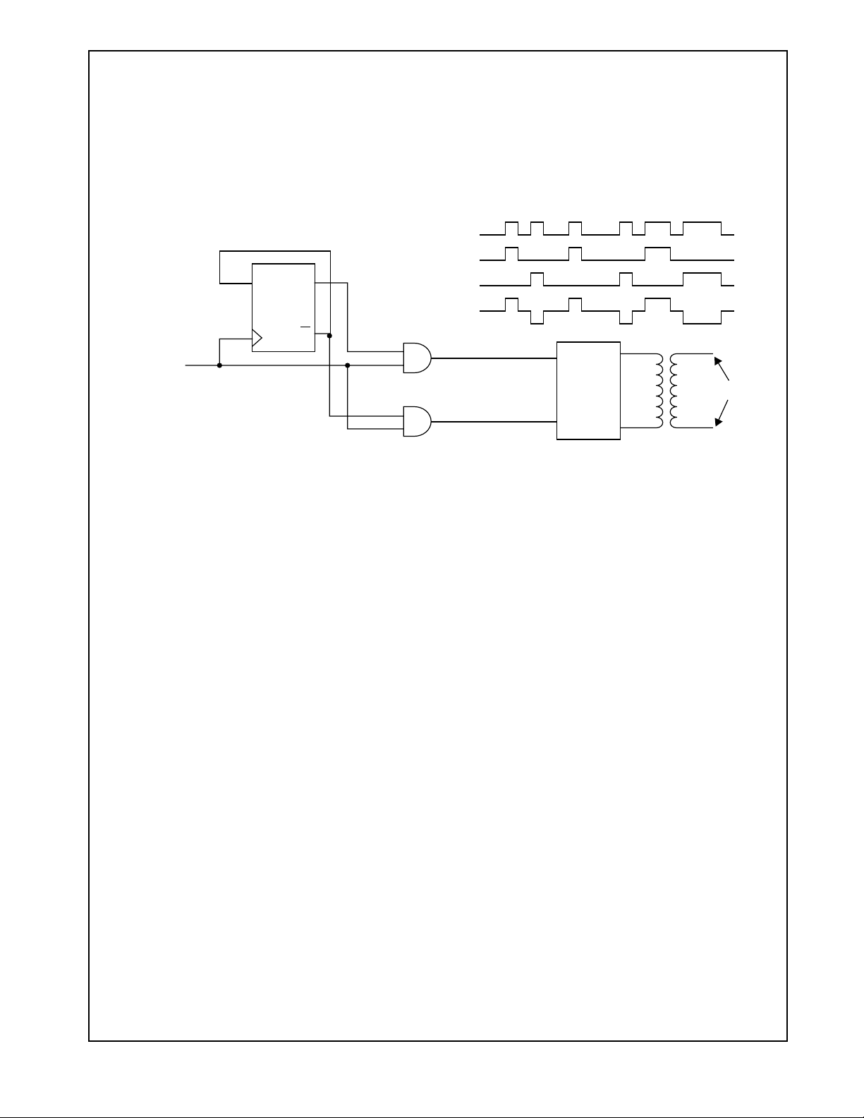
binary_plus
D
binary_in
Q
Q
Figure 6. Binary to MLT-3 conversion
binary_minus
differential MLT-3
3.2.4 Binary to MLT-3 Convertor / Common Driver
The Binary to MLT-3 conversion is accomplished by converting the serial binary data stream output from the NRZI
encoder into two binary data streams with alternately
phased logic one events. These two binary streams are
then fed to the twisted pair output driverwhich converts the
voltage to current and alternately drives either side of the
transmit transformer primary winding, resulting in aminimal
current (20 mA max) MLT-3 signal. Refer to Figure 6 .
binary_in
binary_plus
COMMON
DRIVER
binary_minus
MLT-3
18 www.national.com
Page 19

Table 5. 4B5B Code-Group Encoding/Decoding
Name PCS 5B Code-group MII 4B Nibble Code
DATA CODES
0 11110 0000
1 01001 0001
2 10100 0010
3 10101 0011
4 01010 0100
5 01011 0101
6 01110 0110
7 01111 0111
8 10010 1000
9 10011 1001
A 10110 1010
B 10111 1011
C 11010 1100
D 11011 1101
E 11100 1110
F 11101 1111
IDLE AND CONTROL CODES
H 00100 HALT code-group - Error code
I 11111 Inter-Packet IDLE - 0000 (
Note 1)
J 11000 First Start of Packet - 0101 (Note 1)
K 10001 Second Start of Packet - 0101 (Note 1)
T 01101 First End of Packet - 0000 (Note 1)
R 00111 Second End of Packet - 0000 (Note 1)
INVALID CODES
V 00000
V 00001
V 00010
V 00011
V 00101
V 00110
V 01000
V 01100
V 10000
V 11001
Note 1: Control code-groups I, J, K, T and R in data fields will be mapped as invalid codes, together with RX_ER asserted.
19 www.national.com
Page 20

The 100BASE-TX MLT-3 signal sourced by the TD± common driver output pins is slew rate controlled. This should
be considered when selecting AC coupling magnetics to
ensure TP-PMD Standard compliant transition times (3 ns
< Tr < 5 ns).
The 100BASE-TX transmit TP-PMD function within the
DP83846A is capable of sourcing only MLT-3 encoded
data. Binary output from the TD± outputs is not possible in
100 Mb/s mode.
3.3 100BASE-TX RECEIVER
The 100BASE-TX receiver consists of several functional
blocks which convert the scrambled MLT-3 125 Mb/s serial
data stream to synchronous 4-bit nibble data that is provided to the MII. Because the 100BASE-TX TP-PMD is
integrated, the differential input pins, RD±, can be directly
routed from the AC coupling magnetics.
See Figure 8 for a block diagram of the 100BASE-TX
receive function. This provides an overview of each functional block within the 100BASE-TX receive section.
The Receive section consists of the following functional
blocks:
— ADC
— Input and BLW Compensation
— Signal Detect
— Digital Adaptive Equalization
— MLT-3 to Binary Decoder
— Clock Recovery Module
— NRZI to NRZ Decoder
— Serial to Parallel
— DESCRAMBLER (bypass option)
— Code Group Alignment
— 4B/5B Decoder (bypass option)
— Link Integrity Monitor
— Bad SSD Detection
The bypass option for the functional blocks within the
100BASE-TX receiver provides flexibility for applications
where data conversion is not always required.
3.3.1 Input and Base Line Wander Compensation
Unlike the DP83223V Twister, the DP83846A requires no
external attenuation circuitry at its receive inputs, RD±. It
accepts TP-PMD compliant waveforms directly, requiring
only a 100Ω termination plus a simple 1:1 transformer.
Figure 7. 100BASE-TX BLW Event
The DP83846A is completely ANSI TP-PMD compliant and
includes Base Line Wander (BLW) compensation. The
BLW compensation block can successfully recover the TPPMD defined “killer” pattern and pass it to the digital adaptive equalization block.
BLW can generally be defined as the change in the average DC content, over time, of an AC coupled digital transmission over a given transmission medium. (i.e., copper
wire).
BLW results from the interaction between the low frequency components of a transmitted bit stream and thefre-
quency response of the AC coupling component(s) within
the transmission system.If the low frequency content of the
digital bit stream goes below the low frequency pole of the
AC coupling transformers then the droop characteristics of
the transformers will dominate resulting in potentially serious BLW.
The digital oscilloscope plot provided in Figure 7 illustrates
the severity of the BLW event that can theoretically be generated during 100BASE-TX packet transmission. This
event consists of approximately 800 mV of DC offset for a
period of 120 µs. Left uncompensated, events such as this
can cause packet loss.
20 www.national.com
Page 21

RX_CLK
RXD[3:0] / RX_ER
CLOCK
CLOCK
RECOVERY
MODULE
5
BP_SCR
BP_4B5B
MUX
4B/5BDECODER
SERIAL TO
PARALLEL
CODE GROUP
ALIGNMENT
MUX
DESCRAMBLER
NRZI TO NRZ
DECODER
LINK STATUS
MLT-3 TO
BINARY
DECODER
DIGITAL
ADAPTIVE
EQUALIZATION
AGC
INPUT BLW
COMPENSATION
ADC
RD±
Figure 8. Receive Block Diagram
LINK
MONITOR
SIGNAL
DETECT
21 www.national.com
Page 22

3.3.2 Signal Detect
The signal detect function of the DP83846A is incorporated
to meet the specificationsmandated by the ANSI FDDI TPPMD Standard as well as the IEEE 802.3 100BASE-TX
Standard for both voltage thresholds and timing parameters.
Note that the reception of normal 10BASE-T link pulses
and fast link pulses per IEEE 802.3u Auto-Negotiation by
the 100BASE-TX receiver do not cause the DP83846A to
assert signal detect.
3.3.3 Digital Adaptive Equalization
When transmitting data at high speeds over copper twisted
pair cable, frequency dependent attenuation becomes a
concern. In high-speed twisted pair signalling, the frequency content of the transmitted signal can vary greatly
during normal operation based primarily on the randomness of the scrambled data stream. This variation in signal
attenuation caused by frequency variations must be compensated for to ensure the integrity of the transmission.
In order to ensure quality transmission when employing
MLT-3 encoding, the compensation must be able to adapt
to various cable lengths and cable types depending on the
installed environment. The selection of long cable lengths
for a given implementation, requires significant compensation which will over-compensate for shorter, less attenuating lengths. Conversely, the selection of short or
intermediate cablelengths requiring less compensation will
cause serious under-compensation for longer length
cables. The compensation or equalization must be adaptive to ensure proper conditioning of the received signal
independent of the cable length.
The DP83846A utilizes a extremely robust equalization
scheme referred as ‘Digital Adaptive Equalization’. Traditional designs use a pseudo adaptive equalization scheme
that determines the approximate cable length by monitoring signal attenuation at certain frequencies. This attenuation value was compared to the internal receive input
reference voltage. This comparison would indicate
amount of equalization to use. Although this scheme is
used successfully on the DP83223V twister, it is sensitive
to transformer mismatch, resistor variation and process
induced offset. The DP83223V also required an external
attenuation network to help match the incoming signal
amplitude to the internal reference.
The Digital Equalizer removes ISI (inter symbol interference) from the receive data stream by continuously adapting to provide a filter with the inverse frequency response
of the channel. When used in conjunction with a gain
stage, this enables the receive 'eye pattern' to be opened
sufficiently to allow very reliable data recovery.
Traditionally 'adaptive' equalizers selected 1 of N filters in
an attempt to match the cables characteristics. This
approach will typically leave holes at certain cable lengths,
where the performance of the equalizer is not optimized.
The DP83846A equalizer is truly adaptive to any length of
cable up to 150m.
3.3.4 Clock Recovery Module
The Clock Recovery Module (CRM) accepts 125 Mb/s
MLT3 data from the equalizer. The DPLL locks onto the
125 Mb/s data stream and extracts a 125 MHz recovered
clock. The extracted and synchronized clock and data are
the
used as required by the synchronous receiveoperations as
generally depicted in Figure 8.
The CRM is implemented using an advanced all digital
Phase Locked Loop (PLL) architecture that replaces sensitive analog circuitry. Using digital PLL circuitry allows the
DP83846A to be manufactured and specified to tighter tolerances.
3.3.5 NRZI to NRZ
In a typical application, the NRZI to NRZ decoder is
required in order to present NRZ formatted data to the
descrambler (or to the code-group alignment block, if the
descrambler is bypassed, or directly to the PCS, if the
receiver is bypassed).
3.3.6 Serial to Parallel
The 100BASE-TX receiver includes a Serial to Parallel
converter which supplies 5-bit wide data symbols to the
PCS Rx state machine.
3.3.7 Descrambler
A serial descrambler is used to de-scramble the received
NRZ data. The descrambler has to generate an identical
data scrambling sequence (N) in order to recover the original unscrambled data (UD) from the scrambled data (SD)
as represented in the equations:
SD UD N⊕()=
UD SD N⊕()=
Synchronization of the descrambler to the original scrambling sequence (N) is achieved based on the knowledge
that the incoming scrambled data stream consists of
scrambled IDLE data. After the descrambler has recognized 12 consecutive IDLE code-groups, where an
unscrambled IDLE code-group in 5B NRZ is equal to five
consecutive ones (11111), it will synchronize to the receive
data stream and generate unscrambled data in the form of
unaligned 5B code-groups.
In order to maintain synchronization, the descrambler must
continuously monitor the validity of the unscrambled data
that it generates. To ensure this, a line state monitor and a
hold timer are used to constantly monitor the synchronization status. Upon synchronization of the descrambler the
hold timer starts a 722 µs countdown. Upon detection of
sufficient IDLE code-groups (58 bit times) within the 722 µs
period, the hold timer will reset and begin a new countdown. This monitoring operation will continue indefinitely
given a properly operating network connection with good
signal integrity. If the line state monitor does not recognize
sufficient unscrambled IDLE code-groups within the 722 µs
period, the entire descrambler will be forced out of the current state of synchronization and reset in order to reacquire synchronization.
3.3.8 Code-group Alignment
The code-group alignment module operates on unaligned
5-bit data from the descrambler (or, if the descrambler is
bypassed, directly from the NRZI/NRZ decoder) and converts it into 5B code-group data (5 bits). Code-group alignment occurs after the J/K code-group pair is detected.
Once the J/K code-group pair (11000 10001) is detected,
subsequent data is aligned on a fixed boundary.
22 www.national.com
Page 23

3.3.9 4B/5B Decoder
The code-group decoder functions as a look up table that
translates incoming 5B code-groups into 4B nibbles. The
code-group decoder first detects the J/K code-group pair
preceded by IDLE code-groups and replaces the J/K with
MAC preamble. Specifically, the J/K 10-bit code-group pair
is replaced by the nibble pair (0101 0101). All subsequent
5B code-groups are converted to the corresponding 4B
nibbles for the duration of the entire packet. This conversion ceases upon the detection of the T/R code-group pair
denoting the End of Stream Delimiter (ESD) or with the
reception of a minimum of two IDLE code-groups.
3.3.10 100BASE-TX Link Integrity Monitor
The 100 Base TX Linkmonitor ensures thata valid andstable link is established before enabling both the Transmit
and Receive PCS layer.
Signal detect must be valid for 395us to allow the link monitor to enter the'Link Up'state, and enable the transmit and
receive functions.
3.3.11 Bad SSD Detection
A Bad Start ofStream Delimiter (Bad SSD) isany transition
from consecutive idle code-groups to non-idle code-groups
which is not prefixed by the code-group pair /J/K.
If this condition is detected, the DP83846A will assert
RX_ER and present RXD[3:0] = 1110 to the MII for the
cycles that correspond to received 5B code-groups until at
least two IDLE code groups are detected. In addition, the
False Carrier Sense Counter register (FCSCR) will be
incremented by one.
Once at least two IDLE code groups are detected, RX_ER
and CRS become de-asserted.
3.4 10BASE-T TRANSCEIVER MODULE
The 10BASE-T Transceiver Module is IEEE 802.3 compliant. It includes the receiver, transmitter, collision, heartbeat, loopback, jabber, and link integrity functions, as
defined in the standard. An external filter is not required on
the 10BASE-T interface since this is integrated inside the
DP83846A. This section focuses on the general 10BASE-T
system level operation.
3.4.1 Operational Modes
The DP83846A has two basic 10BASE-T operational
modes:
— Half Duplex mode
— Full Duplex mode
Half Duplex Mode
In Half Duplex mode the DP83846A functions as a standard IEEE 802.3 10BASE-T transceiver supporting the
CSMA/CD protocol.
Full Duplex Mode
In Full Duplex mode the DP83846A is capable of simultaneously transmitting and receiving without asserting the
collision signal. The DP83846A's 10 Mb/s ENDEC is
designed to encode and decode simultaneously.
3.4.2 Collision Detection and SQE
When in Half Duplex, a 10BASE-T collision is detected
when the receive and transmit channels are active simultaneously. Collisions are reported by the COL signal on the
MII. Collisions are also reported when a jabber condition is
detected.
The COL signal remains setfor the durationof the collision.
If the ENDEC is receiving when a collision is detected it is
reported immediately (through the COL pin).
When heartbeat is enabled, approximately 1 µs after the
transmission of each packet, a Signal Quality Error (SQE)
signal of approximately10-bit times isgenerated to indicate
successful transmission. SQE is reported asa pulseon the
COL signal of the MII.
The SQEtest is inhibited when the PHY is set in full duplex
mode. SQE can also be inhibited by setting the
HEARTBEAT_DIS bit in the 10BTSCR register.
3.4.3 Carrier Sense
Carrier Sense(CRS) may be asserted due to receive activity once valid data is detected via the squelch function.
For 10 Mb/s Half Duplex operation, CRS is asserted during
either packet transmission or reception.
For 10 Mb/s Full Duplex operation, CRS is asserted only
during receive activity.
CRS is deasserted following an end of packet.
3.4.4 Normal Link Pulse Detection/Generation
The link pulse generator produces pulses as defined in the
IEEE 802.3 10BASE-T standard. Each link pulse is nominally 100 ns in duration and transmitted every 16 ms in the
absence of transmit data.
Link pulses are used to check the integrity of the connection with the remote end. If valid link pulses are not
received, the link detector disables the 10BASE-T twisted
pair transmitter, receiver and collision detection functions.
When the link integrity function is disabled
(FORCE_LINK_10 of the 10BTSCR register), good link is
forced and the 10BASE-T transceiver will operate regardless of the presence of link pulses.
3.4.5 Jabber Function
The jabber function monitors the DP83846A's output and
disables the transmitter if it attempts to transmit a packetof
longer than legal size. A jabber timer monitors the transmitter and disables the transmission if the transmitter is active
beyond the Jab time (20-150 ms).
Once disabled by the Jabber function, the transmitter stays
disabled for the entire time that the ENDEC module's internal transmit enable is asserted. This signal has to be deasserted for approximately 250-750 ms (the “unjab” time)
before the Jabber function re-enables the transmit outputs.
The Jabber function is only relevant in 10BASE-T mode.
3.4.6 Automatic Link Polarity Detection and Correction
The DP83846A's 10BASE-T transceiver module incorporates an automatic link polarity detection circuit. When
seven consecutive inverted link pulses are received,
inverted polarity is reported.
23 www.national.com
Page 24

A polarity reversal can be caused by a wiring error at either
end of the cable, usually at the Main Distribution Frame
(MDF) or patch panel in the wiring closet.
The inverse polarity condition is latched in the 10BTSCR
register. The DP83846A's 10BASE-T transceiver module
corrects for this error internally and will continue to decode
received data correctly. This eliminates the need to correct
the wiring error immediately.
The user is cautioned that if Auto Polarity Detection and
Correction is disabled and inverted Polarity is detected but
not corrected, the DsPHYTER may falsely report Good
Link status and allow Transmission and Reception of
inverted data. It is recommended that Auto Polarity Detection and Correction not be disabled during normal operation.
3.4.7 Transmit and Receive Filtering
External 10BASE-T filters are not required when using the
DP83846A, as the required signal conditioning is integrated into the device.
Only isolation/step-up transformers and impedance matching resistors are required for the 10BASE-T transmit and
receive interface. The internal transmit filtering ensures
that all the harmonics in the transmit signal are attenuated
by at least 30 dB.
3.4.8 Transmitter
The encoder begins operation when the Transmit Enable
input (TX_EN) goes high and converts NRZ data to preemphasized Manchester data for the transceiver. For the
duration of TX_EN, the serialized Transmit Data (TXD) is
encoded for the transmit-driver pair (TD±). TXD must be
valid on therising edgeof TransmitClock (TX_CLK). Transmission ends when TX_ENdeasserts. The last transition is
always positive; it occurs at the center of the bit cell if the
last bit is a one, orat the end of the bit cell if the last bit is a
zero.
3.4.9 Receiver
The decoderconsists of a differentialreceiver and a PLL to
separate a Manchester encoded data stream into internal
clock signals and data. The differentialinput must be externally terminated with a differential 100Ω termination network to accommodate UTP cable. The impedance of RD
(typically 1.1KΩ) is in parallel with the two 54.9Ω resistors
as is shown in Figure 9 below to approximate the 100Ω
termination.
The decoder detects theend ofa framewhen noadditional
mid-bit transitions are detected. Within one and a half bit
times after the last bit, carrier sense is de-asserted.
3.5 TPI Network Circuit
Figure 9 shows the recommended circuit for a 10/100 Mb/s
twisted pair interface. Below is a partial list of recommended transformers. Is is important that the user realize
that variations with PCB and component characteristics
requires that the application be tested to ensure that the
circuit meets the requirements of the intended application.
Pulse H1012B
Halo TG22-S052ND
Valor PT4171
BELFUSE S558-5999-K2
BELFUSE S558-5999-46
RD-
RD+
TD-
TD+
0.1 F*
Vdd
0.1 F*
49.9Ω
54.9Ω
54.9
Ω
49.9 Ω
TRANSFORMER CENTER
0.1µF
Figure 9. 10/100 Mb/s Twisted Pair Interface
COMMON MODE CHOKES
MAY BE REQUIRED.
1:1
T1
1:1
* PLACE CAPACITORS
CLOSE TO THE
TAPS
RDRD+
TDTD+
RJ45
24 www.national.com
Page 25

3.6 ESD Protection
Typically, ESD precautions are predominantly in effect
when handling the devices or board before being installed
in a system. In those cases, strict handling procedures can
be implemented during the manufacturing process to
greatly reduce the occurrences of catastrophic ESD
events. After the system is assembled, internal components are usually relatively immune from ESD events.
In the case of an installed Ethernet system however, the
network interface pins are still susceptible to external ESD
events. For example, a category 5 cable being dragged
across a carpet has the potential of developing a charge
well above the typical ESD rating of a semiconductor
device.
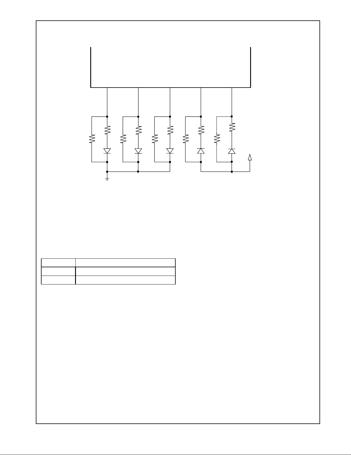
DP83846A 10/100
5V Vcc
TX
For applications where high reliability is required, it is recommended that additional ESD protectiondiodes be added
as shown below. There are numerous dual series connected diode pairs that are available specifically for ESD
protection. The level of protection will vary dependent upon
the diode ratings. The primary parameter that affects the
level of ESD protection is peak forward surge current. Typical specifications for diodes intended for ESD protection
range from 500mA (Motorola BAV99LT1 single pair diodes)
to 12A (STM DA108S1 Quad pair array). The user should
also select diodes with low input capacitance to minimize
the effect on system performance.
Since performance is dependent upon components used,
board impedance characteristics, and layout, the circuit
should be completely tested to ensure performance to the
required levels.
3.3V Vcc
RJ-45
PIN 1
PIN 2
DIODES PLACED
ON THE DEVICE
SIDE OF THE
ISOLATION
TRANSFORMER
RX
Figure 10. Typical DP83846A Network Interface with additional ESD protection
5V Vcc
PIN 3
PIN 6
25 www.national.com
Page 26

3.7 Crystal Oscillator Circuit
The DsPHYTER supports an external CMOS level oscillator source or a crystal resonator device. If an external clock
source is used, X1 should be tied to the clock source and
X2 should be left floating. In either case, the clock source
must be a 25 MHz 0.005% (50 PPM) source. Figure 11
below shows a typical connection for a crystal resonator
circuit. The load capacitor values will vary with the crystal
vendors; check with the vendor for the recommended
loads.
The oscillator circuit was designed to drive a parallel resonance AT cut crystal with a maximum drive level of 500µW.
If a crystal is specified for a lower drive level, a current limiting resistor should be placed in series between X2 and
the crystal.
4.0 Reset Operation
The DP83846A can be reset either by hardware or software. A hardware reset may be accomplished by asserting
the RESET pin after powering up the device (this is
required) or during normal operation when a reset is
needed. A software reset is accomplished by setting the
reset bit in the Basic Mode Control Register.
While either the hardware or software reset can be implemented at any time after device initialization, a hardware
reset, as described in Section 4.1 must be provided upon
device power-up/initialization. Omitting the hardware reset
operation during the device power-up/initialization
sequence can result in improper device operation.
4.1 Hardware Reset
A hardware reset is accomplished by applying a low pulse
(TTL level), with a duration of at least 160µs, to the RESET
pin during normal operation. This will reset the device such
As a starting point for evaluating an oscillator circuit, if the
requirements for the crystal are not known, C
should be set at 22 pF, and R1 should be set at 0Ω.
X1
C
L1
X2
and C
L1
R
1
C
L2
L2
Figure 11. Crystal Oscillator Circuit
that all registers will be reset to default values and the
hardware configuration values will be re-latched into the
device (similar to the power-up/reset operation).
4.2 Software Reset
A software resetis accomplished bysetting the reset bit (bit
15) of the Basic Mode Control Register (BMCR). The
period from the point in time when the reset bit is set to the
point in time when software reset has concluded is approximately 160 µs.
The software reset will reset the device such that all registers willbe reset to default values and the hardwareconfiguration values will be re-latched into the device (similar to
the power-up/reset operation). Software driver code should
wait 300 µs following a software reset before allowing further serial MII operations with the DP83846A.
Vcc
HARDWARE
RESET
MDC
Latch-In of Hardware
Configuration Pins
Dual Function Pins
Become Enabled As Outputs
160 µs
3 µs
3 µs
INPUT
Figure 12. Power-on Reset Examples
32 CLOCKS
50 ns
OUTPUT
26 www.national.com
Page 27

5.0 Register Block
Table 6. Register Map
Offset
Hex Decimal
00h 0 RW BMCR Basic Mode Control Register
01h 1 RO BMSR Basic Mode Status Register
02h 2 RO PHYIDR1 PHY Identifier Register #1
03h 3 RO PHYIDR2 PHY Identifier Register #2
04h 4 RW ANAR Auto-Negotiation Advertisement Register
05h 5 RW ANLPAR Auto-Negotiation Link Partner Ability Register (Base Page)
05h 5 RW ANLPARNP Auto-Negotiation Link Partner Ability Register (Next Page)
06h 6 RW ANER Auto-Negotiation Expansion Register
07h 7 RW ANNPTR Auto-Negotiation Next Page TX
08h-Fh 8-15 RESERVED RESERVED
10h 16 RO PHYSTS PHY Status Register
11h-13h 17-19 RESERVED RESERVED
14h 20 RW FCSCR False Carrier Sense Counter Register
15h 21 RW RECR Receive Error Counter Register
16h 22 RW PCSR PCS Sub-Layer Configuration and Status Register
17h 23 RW RESERVED RESERVED
18h 24 RW RESERVED RESERVED
19h 25 RW PHYCTRL PHY Control Register
1Ah 26 RW 10BTSCR 10Base-T Status/Control Register
1Bh 27 RW CDCTRL CD Test Control Register
1Ch-1Fh 28 RW RESERVED RESERVED
Access Tag Description
Extended Registers
27 www.national.com
Page 28

Register Name Addr Tag Bit 15 Bit 14 Bit 13 Bit 12 Bit 11 Bit 10 Bit 9 Bit 8 Bit 7 Bit 6 Bit 5 Bit 4 Bit 3 Bit 2 Bit 1 Bit 0
Basic Mode Control Register
Basic Mode Status Register
PHY Identifier Register 1
PHY Identifier Register 2
Auto-Negotiation Advertisement Register
Auto-NegotiationLinkPartnerAbilityRegister (Base Page)
Auto-NegotiationLinkPartnerAbilityRegister Next Page
Auto-Negotiation Expansion Register
Auto-Negotiation Next Page TX Register
RESERVED
28 www.national.com
PHY Status Register
RESERVED
False Carrier Sense Counter Register
Receive Error Counter Register
PCS Sub-Layer Configuration and Status
Register
RESERVED
PHY Control Register
10Base-T Status/Control Register
CD Test Control Register
RESERVED
00h BMCR Reset Loopback Speed
01h BMSR 100Base-T4100Base-
02h PHYIDR1 OUI MSB OUI MSB OUI MSB OUI MSB OUI MSB OUI MSB OUI MSB OUI MSB OUI MSB OUI MSB OUI MSB OUI MSB OUI MSB OUI MSB OUI MSB OUI MSB
03h PHYIDR2 OUI LSB OUI LSB OUI LSB OUI LSB OUI LSB OUI LSB VNDR_
04h ANAR Next
05h ANLPAR Next
05h AN-
LPARNP
06h ANER Reserved Reserved Reserved Reserved Reserved Reserved Reserved Reserved Reserved Reserved Reserved PDF LP_NP_
07h ANNPTR Next
08-0fh Reserved Reserved Reserved Reserved Reserved Reserved Reserved Reserved Reserved Reserved Reserved Reserved Reserved Reserved Reserved Reserved Reserved
Page Ind
Page Ind
Next
Page Ind
Page Ind
TX FDX
Reserved Remote
ACK Remote
ACK Message
Reserved Message
Auto-Neg
Select
100Base-
10Base-
TX HDX
Reserved Reserved PAUSE T4 TX_FD TX 10_FD 10 Protocol
Fault
Reserved Reserved Reserved T4 TX_FD TX 10_FD 10 Protocol
Fault
Page
Page
Power
Enable
10Base-
T
FDXx
ACK2 Toggle Code Code Code Code Code Code Code Code Code Code Code
ACK2 TOG_TX CODE CODE CODE CODE CODE CODE CODE CODE CODE CODE CODE
Isolate Restart
down
T
HDX
Auto-Neg
Reserved Reserved Reserved Reserved MF Pre-
MDL
Duplex Collision
VNDR_
MDL
Test
VNDR_
MDL
Reserved Reserved Reserved Reserved Reserved Reserved Reserved
amble
Suppress
VNDR_
MDL
Auto-Neg
Complete
VNDR_
MDL
Remote
Fault
VNDR_
MDL
Selection
Selection
Auto-Neg
Ability
MDL_
REV
Protocol
Selection
Protocol
Selection
ABLE
Link
Status
MDL_
REV
Protocol
Selection
Protocol
Selection
NP_
ABLE
Jabber
Extended
Detect
Capability
MDL_
MDL_
REV
REV
Protocol
Selection
Selection
Protocol
Selection
Protocol
Protocol
Selection
PAGE_RXLP_AN_
ABLE
EXTENDED REGISTERS
10h PHYSTS Reserved Reserved Rx Err
11-13h Reserved Reserved Reserved Reserved Reserved Reserved Reserved Reserved Reserved Reserved Reserved Reserved Reserved Reserved Reserved Reserved Reserved
14h FCSCR Reserved Reserved Reserved Reserved Reserved Reserved Reserved Reserved FCSCNT FCSCNT FCSCNT FCSCNT FCSCNT FCSCNT FCSCNT FCSCNT
15h RECR Reserved Reserved Reserved Reserved Reserved Reserved Reserved Reserved RXER-
16h PCSR Reserved Reserved Reserved BYP_
17-18h Reserved Reserved Reserved Reserved Reserved Reserved Reserved Reserved Reserved Reserved Reserved Reserved Reserved Reserved Reserved Reserved Reserved
19h PHYCTRL Unused Unused Unused Unused PSR_15 BIST_
1Ah 10BTSCR Unused Unused Unused Unused Unused Unused Unused Loopback
1Bh CDCTRL CD_EnableDCD_
1C-1Fh Reserved Reserved Reserved Reserved Reserved Reserved Reserved Reserved Reserved Reserved Reserved Reserved Reserved Reserved Reserved Reserved Reserved
Comp
FIL_TTL rise-
Latch
Polarity
Status
4B5B
Time[1]
False Car-
Signal De-
rier Sense
FREE_
CLK
rise-
fallTime[1] fallTime[0] cdTestEn Reserved Reserved Reserved cdPattEn
Time[0]
Descram
tect
Lock
TQ_EN SD_FOR
CE_PMA
STATUS
BIST_
START
Page
Receive
SD_
OPTION
BP_
STRETC
H
_10_dis
Reserved Remote
Unused Reserved FORCE_
PAUSE_
LP_DIS Force_
CNT
STS
Fault
RXER-
CNT
LED_
CNFG
Link_10
Jabber
Auto-Neg
Detect
Complete
RXER-
RXER-
CNT
CNT
Reserved Reserved NRZI_
100_OK
LED_
CNFG
Force_
Pol_Cor
PHY
ADDR
Polarity Autopol
_10
Loopback
Status
RXER-
CNT
PHY
ADDR
_Dis
cdPatEn_
100
Duplex
Speed
Status
Status
RXER-
RXER-
CNT
CNT
SCRAM_
BYPASS
BYPASSDESCRAM_
PHY
ADDR
Reserved Hrtbeat
10meg_
patt_gap
PHY
ADDR
_Dis
cdPatt-
Sel[1]
Link
Status
RXER-
CNT
BYPASS
PHY
ADDR
Jabber
_Dis
cdPatt-
Sel[0]
Page 29

5.1 Register Definition
In the register definitions under the ‘Default’ heading, the following definitions hold true:
— RW=Read Write access
SC=Register sets on event occurrence and Self-Clears when event ends
—
— RW/SC =Read Write access/Self Clearing bit
— RO=Read Only access
— COR = Clear on Read
— RO/COR=Read Only, Clear on Read
— RO/P=Read Only, Permanently set to a default value
— LL=Latched Low and held until read, based upon the occurrence of the corresponding event
— LH=Latched High and held until read, based upon the occurrence of the corresponding event
29 www.national.com
Page 30

Table 7. Basic Mode Control Register (BMCR), Address 0x00
Bit Bit Name Default Description
15 Reset 0, RW/SC Reset:
1 = Initiate software Reset / Reset in Process.
0 = Normal operation.
This bit, which is self-clearing, returns a value of one until the reset process is
complete. The configuration is re-strapped.
14 Loopback 0, RW Loopback:
1 = Loopback enabled.
0 = Normal operation.
The loopback function enables MII transmit data to be routed to the MII receive
data path.
Setting this bit maycause the descrambler tolose synchronization and producea
500 µs “dead time” before any valid data will appear at the MII receive outputs.
13 Speed Selection Strap, RW Speed Select:
When auto-negotiation is disabledwriting tothis bitallowsthe port speed tobe selected.
1 = 100 Mb/s.
0 = 10 Mb/s.
12 Auto-Negotiation
Enable
11 Power Down 0, RW Power Down:
10 Isolate 0, RW Isolate:
9 Restart Auto-
Negotiation
8 Duplex Mode Strap, RW Duplex Mode:
7 Collision Test 0, RW Collision Test:
6:0 RESERVED 0, RO RESERVED: Write ignored, read as 0.
Strap, RW Auto-Negotiation Enable:
Strap controls initial value at reset.
1 = Auto-Negotiation Enabled- bits 8 and13 of this registerare ignored when this
bit is set.
0=Auto-NegotiationDisabled - bits 8 and 13 determine the port speed and duplex
mode.
1 = Power down.
0 = Normal operation.
Setting this bit powers down the PHY.Only the register block isenabled during a
power down condition.
1 = Isolates the Port from the MII with the exception of the serial management.
0 = Normal operation.
0, RW/SC Restart Auto-Negotiation:
1 = Restart Auto-Negotiation. Re-initiates the Auto-Negotiation process. If AutoNegotiation is disabled (bit 12 = 0), this bit is ignored. This bit is self-clearingand
will return a value of 1 until Auto-Negotiation is initiated, whereupon it will selfclear. Operation of the Auto-Negotiation process is not affected by the management entity clearing this bit.
0 = Normal operation.
When auto-negotiation is disabled writing to this bit allows the port Duplex capability to be selected.
1 = Full Duplex operation.
0 = Half Duplex operation.
1 = Collision test enabled.
0 = Normal operation.
When set, this bit will cause the COL signal to be asserted in response to the as-
sertion ofTX_EN within 512-bit times. The COL signal will bede-asserted within
4-bit times in response to the de-assertion of TX_EN.
30 www.national.com
Page 31

Table 8. Basic Mode Status Register (BMSR), address 0x01
Bit Bit Name Default Description
15 100BASE-T4 0, RO/P 100BASE-T4 Capable:
0 = Device not able to perform 100BASE-T4 mode.
14 100BASE-TX
Full Duplex
13 100BASE-TX
Half Duplex
12 10BASE-T
Full Duplex
11 10BASE-T
Half Duplex
10:7 RESERVED 0, RO RESERVED: Write as 0, read as 0.
6 MF Preamble
Suppression
5 Auto-Negotiation
Complete
4 Remote Fault 0, RO/LH Remote Fault:
3 Auto-Negotiation
Ability
2 Link Status 0, RO/LL Link Status:
1 Jabber Detect 0, RO/LH Jabber Detect: This bit only has meaning in 10 Mb/s mode.
0 Extended Capabili-
ty
1, RO/P 100BASE-TX Full Duplex Capable:
1 = Device able to perform 100BASE-TX in full duplex mode.
1, RO/P 100BASE-TX Half Duplex Capable:
1 = Device able to perform 100BASE-TX in half duplex mode.
1, RO/P 10BASE-T Full Duplex Capable:
1 = Device able to perform 10BASE-T in full duplex mode.
1, RO/P 10BASE-T Half Duplex Capable:
1 = Device able to perform 10BASE-T in half duplex mode.
1, RO/P Preamble suppression Capable:
1 = Device able to perform management transaction with preamble
suppressed,32-bitsofpreambleneeded only once after reset, invalid
opcode or invalid turnaround.
0 = Normal management operation.
0, RO Auto-Negotiation Complete:
1 = Auto-Negotiation process complete.
0 = Auto-Negotiation process not complete.
1 = Remote Fault condition detected (cleared on read or by reset).
Fault criteria: Far End Fault Indication or notification from Link Partner of Remote Fault.
0 = No remote fault condition detected.
1, RO/P Auto Negotiation Ability:
1 = Device is able to perform Auto-Negotiation.
0 = Device is not able to perform Auto-Negotiation.
1 = Valid link established (for either 10 or 100 Mb/s operation).
0 = Link not established.
Thecriteriaforlinkvalidity is implementation specific. The occurrence
of a link failureconditionwill causes the LinkStatus bit to clear.Once
cleared, this bitmay only beset by establishinga good linkcondition
and a read via the management interface.
1 = Jabber condition detected.
0 = No Jabber.
This bit is implemented with a latching function, such that the occur-
rence of a jabbercondition causes it toset until it isclearedby a read
to this register by the management interface or by a reset.
1, RO/P Extended Capability:
1 = Extended register capabilities.
0 = Basic register set capabilities only.
31 www.national.com
Page 32

The PHY Identifier Registers #1 and #2 together form a unique identifier for the DP83846A. The Identifier consists of a
concatenation of the Organizationally Unique Identifier (OUI), the vendor's model number and the model revision number.A PHY mayreturn avalue of zeroin each ofthe 32 bits of thePHY Identifier if desired. ThePHY Identifier is intended
to support network management. National's IEEE assigned OUI is 080017h.
Table 9. PHY Identifier Register #1 (PHYIDR1), address 0x02
Bit Bit Name Default Description
15:0 OUI_MSB <0010 0000 0000
0000>, RO/P
Table 10. PHY Identifier Register #2 (PHYIDR2), address 0x03
Bit Bit Name Default Description
15:10 OUI_LSB <01 0111>, RO/P OUI Least Significant Bits:
9:4 VNDR_MDL <00 0010>, RO/P Vendor Model Number:
3:0 MDL_REV <0000>, RO/P Model Revision Number:
OUI Most Significant Bits: Bits 3 to 18 of the OUI (080017h) are
stored in bits 15 to 0 of this register. The most significant two bits
of the OUI are ignored(the IEEE standard refers tothese as bits 1
and 2).
Bits 19 to 24 of the OUI (080017h) are mapped to bits 15 to 10 of
this register respectively.
The six bits of vendor model number are mapped to bits 9 to 4
(most significant bit to bit 9).
Four bits of the vendor model revision number aremapped to bits
3 to 0 (most significantbitto bit 3). Thisfield willbe incrementedfor
all major device changes.
32 www.national.com
Page 33

This register contains the advertised abilities of this device as they will be transmitted to its link partner during AutoNegotiation.
Table 11. Auto-Negotiation Advertisement Register (ANAR), address 0x04
Bit Bit Name Default Description
15 NP 0, RW Next Page Indication:
0 = Next Page Transfer not desired.
1 = Next Page Transfer desired.
14 RESERVED 0, RO/P RESERVED by IEEE: Writes ignored, Read as 0.
13 RF 0, RW Remote Fault:
1 = Advertises that this device has detected a Remote Fault.
0 = No Remote Fault detected.
12:11 RESERVED 0, RW RESERVED for Future IEEE use: Write as 0, Read as 0
10 PAUSE Strap, RW PAUSE: The default is set by the strap option for
1 = Advertise that the DTE (MAC) has implemented both the op-
tional MAC control sublayer and the pause functionas specified in
clause 31 and annex 31B of 802.3u.
0= No MAC based full duplex flow control.
9 T4 0, RO/P 100BASE-T4 Support:
1= 100BASE-T4 is supported by the local device.
0 = 100BASE-T4 not supported.
8 TX_FD Strap, RW 100BASE-TX Full Duplex Support:
1 = 100BASE-TX Full Duplex is supported by the local device.
0 = 100BASE-TX Full Duplex not supported.
7 TX Strap, RW 100BASE-TX Support:
1 = 100BASE-TX is supported by the local device.
0 = 100BASE-TX not supported.
6 10_FD Strap, RW 10BASE-T Full Duplex Support:
1 = 10BASE-T Full Duplex is supported by the local device.
0 = 10BASE-T Full Duplex not supported.
5 10 Strap, RW 10BASE-T Support:
1 = 10BASE-T is supported by the local device.
0 = 10BASE-T not supported.
4:0 Selector <00001>, RW Protocol Selection Bits:
These bits containthe binary encodedprotocol selector supported
by this port. <00001> indicates that this device supports IEEE
802.3u.
PAUSE_EN pin.
33 www.national.com
Page 34

This register contains the advertised abilities of the Link Partner as received during Auto-Negotiation. The content
changes after the successful autonegotiation if Next-pages are supported.
Table 12. Auto-Negotiation Link Partner Ability Register (ANLPAR) (BASE Page), address 0x05
Bit Bit Name Default Description
15 NP 0, RO Next Page Indication:
0 = Link Partner does not desire Next Page Transfer.
1 = Link Partner desires Next Page Transfer.
14 ACK 0, RO Acknowledge:
1 = Link Partner acknowledges reception of the ability data word.
0 = Not acknowledged.
The Device's Auto-Negotiation state machine will automatically
control the this bit based on the incoming FLP bursts.
13 RF 0, RO Remote Fault:
1 = Remote Fault indicated by Link Partner.
0 = No Remote Fault indicated by Link Partner.
12:10 RESERVED 0, RO RESERVED for Future IEEE use:
Write as 0, read as 0.
9 T4 0, RO 100BASE-T4 Support:
1 = 100BASE-T4 is supported by the Link Partner.
0 = 100BASE-T4 not supported by the Link Partner.
8 TX_FD 0, RO 100BASE-TX Full Duplex Support:
1 = 100BASE-TX Full Duplex is supported by the Link Partner.
0 = 100BASE-TX Full Duplex not supported by the Link Partner.
7 TX 0, RO 100BASE-TX Support:
1 = 100BASE-TX is supported by the Link Partner.
0 = 100BASE-TX not supported by the Link Partner.
6 10_FD 0, RO 10BASE-T Full Duplex Support:
1 = 10BASE-T Full Duplex is supported by the Link Partner.
0 = 10BASE-T Full Duplex not supported by the Link Partner.
5 10 0, RO 10BASE-T Support:
1 = 10BASE-T is supported by the Link Partner.
0 = 10BASE-T not supported by the Link Partner.
4:0 Selector <0 0000>, RO Protocol Selection Bits:
Link Partner’s binary encoded protocol selector.
34 www.national.com
Page 35

Table 13. Auto-Negotiation Link Partner Ability Register (ANLPAR) Next Page, address 0x05
Bit Bit Name Default Description
15 NP 0, RO Next Page Indication:
1 = Link Partner desires Next Page Transfer.
0 = Link Partner does not desire Next Page Transfer.
14 ACK 0, RO Acknowledge:
1 = Link Partner acknowledges reception of the ability data word.
0 = Not acknowledged.
The Device's Auto-Negotiation state machine will automatically
control the this bit based on the incoming FLP bursts. Software
should not attempt to write to this bit.
13 MP 0, RO Message Page:
1 = Message Page.
0 = Unformatted Page.
12 ACK2 0, RO Acknowledge 2:
1 = Link Partnerdoes have the ability to comply to next page mes-
sage.
0 = Link Partner does not have the ability to comply to next page
message.
11 Toggle 0, RO Toggle:
1 = Previous value of the transmitted Link Code word equalled 0.
0 = Previous value of the transmitted Link Code word equalled 1.
10:0 CODE <00000000000>,ROCode:
This field represents the code field of the next page transmission.
If the MP bit is set (bit 13 of this register), then the code shall be
interpreted as a “Message Page”, as defined in annex 28C of
Clause 28. Otherwise, the code shall be interpreted as an “Unfor-
matted Page”, and the interpretation is application specific.
This register contains additional Local Device and Link Partner status information.
Table 14. Auto-Negotiate Expansion Register (ANER), address 0x06
Bit Bit Name Default Description
15:5 RESERVED 0, RO RESERVED: Writes ignored, Read as 0.
4 PDF 0, RO/LH/COR Parallel Detection Fault:
1 = A fault has been detected via the Parallel Detection function.
0 = A fault has not been detected.
3 LP_NP_ABLE 0, RO Link Partner Next Page Able:
1 = Link Partner does support Next Page.
0 = Link Partner does not support Next Page.
2 NP_ABLE 1, RO/P Next Page Able:
1 = Indicates local device is able to send additional “Next Pages”.
1 PAGE_RX 0, RO/LH/COR Link Code Word Page Received:
1 = Link Code Word has been received, cleared on a read.
0 = Link Code Word has not been received.
0 LP_AN_ABLE 0, RO Link Partner Auto-Negotiation Able:
1 = indicates that the Link Partner supports Auto-Negotiation.
0 = indicates that the Link Partner does not support Auto-Negotia-
tion.
35 www.national.com
Page 36

This register contains the next page information sent by this device to its Link Partner during Auto-Negotiation.
Table 15. Auto-Negotiation Next Page Transmit Register (ANNPTR), address 0x07
Bit Bit Name Default Description
15 NP 0, RW Next Page Indication:
0 = No other Next Page Transfer desired.
1 = Another Next Page desired.
14 RESERVED 0, RO RESERVED: Writes ignored, read as 0.
13 MP 1, RW Message Page:
1 = Message Page.
0 = Unformatted Page.
12 ACK2 0, RW Acknowledge2:
1 = Will comply with message.
0 = Cannot comply with message.
Acknowledge2 is used by the nextpage functionto indicatethat Lo-
cal Device has the ability to comply with the message received.
11 TOG_TX 0, RO Toggle:
1 = Value of toggle bit in previously transmitted Link Code Word
was 0.
0 = Value of toggle bit in previously transmitted Link Code Word
was 1.
Toggle is used by the Arbitration function within Auto-Negotiation
to ensure synchronization with the Link Partner during Next Page
exchange. This bit shall alwaystake the opposite value of the Tog-
gle bit in the previously exchanged Link Code Word.
10:0 CODE <00000000001>,RWThis field represents the code field of the next page transmission.
If the MP bit is set (bit 13 of this register), then the code shall be
interpreted as a "MessagePage”, asdefinedin annex 28C ofIEEE
802.3u. Otherwise, the code shall be interpreted as an "Unformat-
ted Page”, and the interpretation is application specific.
The default value of the CODE represents a Null Page as defined
in Annex 28C of IEEE 802.3u.
36 www.national.com
Page 37

5.2 Extended Registers
This register provides a single location within the register set for quick access to commonly accessed information.
Table 16. PHY Status Register (PHYSTS), address 0x10
Bit Bit Name Default Description
15:14 RESERVED 0, RO RESERVED: Write ignored, read as 0.
13 Receive Error Latch 0, RO/LH Receive Error Latch:
This bit will be cleared upon a read of the RECR register.
1 = Receiveerror event has occurredsince last readof RXERCNT
(address 0x15, Page 0).
0 = No receive error event has occurred.
12 Polarity Status 0, RO Polarity Status:
Thisbit is a duplication of bit4 in the10BTSCR register. Thisbit will
be cleared upon a read of the 10BTSCR register, but not upon a
read of the PHYSTS register.
1 = Inverted Polarity detected.
0 = Correct Polarity detected.
11 False CarrierSense
Latch
10 Signal Detect 0, RO/LL 100Base-TX unconditional Signal Detect from PMD.
9 Descrambler Lock 0, RO/LL 100Base-TX Descrambler Lock from PMD.
8 Page Received 0, RO Link Code Word Page Received:
0, RO/LH False Carrier Sense Latch:
This bit will be cleared upon a read of the FCSR register.
1 = False Carrierevent hasoccurredsince last read ofFCSCR (ad-
dress 0x14).
0 = No False Carrier event has occurred.
This is a duplicate of the Page Received bit in the ANER register,
but this bit will not be cleared upon a read of the PHYSTS register.
1 = A new Link Code Word Page has been received. Cleared on
read of the ANER (address 0x06, bit 1).
0 = Link Code Word Page has not been received.
37 www.national.com
Page 38

Table 16. PHY Status Register (PHYSTS), address 0x10 (Continued)
Bit Bit Name Default Description
7 RESERVED 0, RO RESERVED: Writes ignored, Read as 0.
6 Remote Fault 0, RO Remote Fault:
1 = Remote Fault condition detected (cleared on read of BMSR
(address 01h) register or by reset). Fault criteria: notification from
Link Partner of Remote Fault via Auto-Negotiation.
0 = No remote fault condition detected.
5 Jabber Detect 0, RO Jabber Detect: This bit only has meaning in 10 Mb/s mode
This bit is a duplicateofthe Jabber Detect bitin theBMSR register,
except that it is not cleared upon a read of the PHYSTS register.
1 = Jabber condition detected.
0 = No Jabber.
4 Auto-Neg Complete 0, RO Auto-Negotiation Complete:
1 = Auto-Negotiation complete.
0 = Auto-Negotiation not complete.
3 Loopback Status 0, RO Loopback:
1 = Loopback enabled.
0 = Normal operation.
2 Duplex Status 0, RO Duplex:
This bit indicatesduplex status andis determined fromAuto-Negotiation or Forced Modes.
1 = Full duplex mode.
0 = Half duplex mode.
Note: This bit is only valid if Auto-Negotiation is enabled and com-
plete and there is avalid link or if Auto-Negotiation is disabledand
there is a valid link.
1 Speed Status 0, RO Speed10:
This bit indicates the status of the speed and is determined from
Auto-Negotiation or Forced Modes.
1 = 10 Mb/s mode.
0 = 100 Mb/s mode.
Note: This bit is only valid if Auto-Negotiation is enabled and com-
plete and there is avalid link or if Auto-Negotiation is disabledand
there is a valid link.
0 Link Status 0, RO Link Status:
This bit is a duplicate of the Link Status bit in the BMSR register,
except that it will no be cleared upon a read of the PHYSTS register.
1 = Valid link established (for either 10 or 100 Mb/s operation).
0 = Link not established.
38 www.national.com
Page 39

This counter provides information required to implement the “FalseCarriers” attribute within the MAU managed object
class of Clause 30 of the IEEE 802.3u specification.
Table 17. False Carrier Sense Counter Register (FCSCR), address 0x14
Bit Bit Name Default Description
15:8 RESERVED 0, RO RESERVED: Writes ignored, Read as 0
7:0 FCSCNT[7:0] 0, RW / COR False Carrier Event Counter:
This 8-bit counter increments on every false carrier event. This
counter sticks when it reaches its max count (FFh).
This counter provides information required to implement the “SymbolErrorDuringCarrier” attribute within the PHY managed object class of Clause 30 of the IEEE 802.3u specification.
Table 18. Receiver Error Counter Register (RECR), address 0x15
Bit Bit Name Default Description
15:8 RESERVED 0, RO RESERVED: Writes ignored, Read as 0
7:0 RXERCNT[7:0] 0, RW / COR RX_ER Counter:
This 8-bit counter increments for each receive error detected.
When a valid carrier ispresentand there is atleast oneoccurrence
of an invalid data symbol. This event can increment only once per
valid carrier event. If a collision is present, the attribute will not in-
crement. The counter sticks when it reaches its max count.
Table 19. 100 Mb/s PCS Configuration and Status Register (PCSR), address 0x16
Bit Bit Name Default Description
15:13 RESERVED <00>, RO RESERVED: Writes ignored, Read as 0.
12 BYP_4B5B 0, RW Bypass 4B/5B Encoding:
1 = 4B5B encoder functions bypassed.
0 = Normal 4B5B operation.
11 FREE_CLK 0, RW Receive Clock:
1 = RX_CK is free-running.
0 = RX_CK phase adjusted based on alignment.
10 TQ_EN
9 SD FORCE PMA
8 SD_OPTION 1, RW Signal Detect Option:
0, RW
0,RW
100Mbs True Quiet Mode Enable:
1 = Transmit True Quiet Mode.
0 = Normal Transmit Mode.
Signal Detect Force PMA:
1 = Forces Signal Detection in PMA.
0 = Normal SD operation.
1 = Enhanced signal detect algorithm.
0 = Reduced signal detect algorithm.
39 www.national.com
Page 40

Table 19. 100 Mb/s PCS Configuration and Status Register (PCSR), address 0x16 (Continued)
Bit Bit Name Default Description
7 Unused 0,RO
6 RESERVED 0 RESERVED:
Must be zero.
5 FORCE_100_OK 0, RW Force 100Mb/s Good Link:
1 = Forces 100Mb/s Good Link.
0 = Normal 100Mb/s operation.
4 RESERVED 0 RESERVED:
Must be zero.
3 RESERVED 0 RESERVED:
Must be zero.
2 NRZI_BYPASS 0, RW NRZI Bypass Enable:
1 = NRZI Bypass Enabled.
0 = NRZI Bypass Disabled.
1 SCRAM_BYPASS 0, RW Scrambler Bypass Enable:
1 = Scrambler Bypass Enabled.
0 = Scrambler Bypass Disabled.
0 DESCRAM_BYPA
SS
0, RW Descrambler Bypass Enable:
1 = Descrambler Bypass Enabled.
0 = Descrambler Bypass Disabled.
Table 20. Reserved Registers, addresses 0x17, 0x18
Bit Bit Name Default Description
15:0 RESERVED none, RW RESERVED: Must not be written to during normal operation.
40 www.national.com
Page 41

Table 21. PHY Control Register (PHYCTRL), address 0x19
Bit Bit Name Default Description
15:12 Unused 0, RO
11 PSR_15 0, RW BIST Sequence select:
1 = PSR15 selected.
0 = PSR9 selected.
10 BIST_STATUS 0, RO/LL BIST Test Status:
1 = BIST pass.
0 = BIST fail. Latched, cleared by write to BIST_ START bit.
9 BIST_START 0, RW BIST Start:
1 = BIST start.
0 = BIST stop.
8 BP_STRETCH 0, RW Bypass LED Stretching:
This will bypass the LED stretching for the Receive, Transmit and
Collision LEDs.
1 = Bypass LED stretching.
0 = Normal operation.
7 PAUSE_STS 0, RO Pause Compare Status:
0 = Local Device and the Link Partner are not Pause capable.
1 = Local Device and the Link Partner are both Pause capable.
6 RESERVED
5 LED_CNFG
4:0 PHYADDR[4:0] Strap, RW PHY Address: PHY address for port.
1, RO/P
Strap, RW
Reserved: Must be 1.
This bit is used tobypassthe selective inversion on theLEDoutput
for DPLX - this enables its use in non-LED applications.
Mode Description
1 = Led polarity adjusted - DPLX selected.
0 = DPLX active HIGH.
41 www.national.com
Page 42

Table 22. 10Base-T Status/Control Register (10BTSCR), Address 0x1A
Bit Bit Name Default Description
15:9 Unused 0,RO
8 LOOPBACK_10_DIS 0, RW 10Base-T Loopback Disable:
This bit is OR’ed with bit 14 (Loopback) in the BMCR.
1 = 10BT Loopback is disabled.
0 = 10BT Loopback is enabled.
7 LP_DIS 0, RW Normal Link Pulse Disable:
1 = Transmission of NLPs is disabled.
0 = Transmission of NLPs is enabled.
6 FORCE_LINK_10 0, RW Force 10Mb Good Link:
1 = Forced Good 10Mb Link.
0 = Normal Link Status.
5 FORCE_POL_COR 0, RW Force 10Mb Polarity Correction:
1 = Force inverted polarity.
0 = Normal polarity.
4 POLARITY RO/LH 10Mb Polarity Status:
This bitis a duplication of bit 12 in the PHYSTS register. Both bits
will be cleared upon a read of 10BTSCR register, but not upon a
read of the PHYSIS register.
1 = Inverted Polarity detected.
0 = Correct Polarity detected.
3 AUTOPOL_DIS 0, RW Auto Polarity Detection & Correction Disable:
1 = Polarity Sense & Correction disabled.
0 = Polarity Sense & Correction enabled.
2 RESERVED 1, RW RESERVED:
Must be set to one.
1 HEARTBEAT_DIS 0, RW Heartbeat Disable: This bitonly hasinfluence inhalf-duplex 10Mb
0 JABBER_DIS 0, RW Jabber Disable:
mode.
1 = Heartbeat function disabled.
0 = Heartbeat function enabled.
When the device is operating at 100Mb or configured for full
duplex operation, this bit will be ignored - the heartbeat function is disabled.
Applicable only in 10BASE-T.
1 = Jabber function disabled.
0 = Jabber function enabled.
42 www.national.com
Page 43

Table 23. CD Test Register (CDCTRL), Address 0x1B
Bit Bit Name Default Description
15 CD_ENABLE 1, RW CD Enable:
1 = CD Enabled - power-down mode, outputs high impedance.
0 = CD Disabled.
14 DCDCOMP 0, RW Duty Cycle Distortion Compensation:
1 = Increases the amount of DCD compensation.
13 FIL_TTL 0, RW Waveshaper Current Source Test:
To check ability of waveshaper current sources to switch on/off.
1 = Test mode; waveshaping is done, but the output is a square
wave. All sources are either on or off.
0 = Normal mode; sinusoidal.
12 RESERVED none, RW Reserved: This bit should be written with a 0 if write access is re-
11 RISETIME Strap, RW CD Rise Time Control:
10 RESERVED none, RW Reserved: This bit should be written with a 0 if write access is re-
9 FALLTIME Strap, RW CD Fall Time Control:
8 CDTESTEN 0, RW CD Test Mode Enable:
7:5 RESERVED[2:0] 000, RW RESERVED:
4 CDPATTEN_10 0, RW CD Pattern Enable for 10meg:
3 CDPATTEN_100 0, RW CD Pattern Enable for 100meg:
2 10MEG_PATT_GAP 0, RW Defines gap between data or NLP test sequences:
1:0 CDPATTSEL[1:0] 00, RW CD Pattern Select[1:0]:
quired on this register.
quired on this register.
1 = Enable CD test mode - differs based on speed of operation
(10/100Mb).
0 = Normal operation.
Must be zero.
1 = Enabled.
0 = Disabled.
1 = Enabled.
0 = Disabled.
1 = 15 µs.
0 = 10 µs.
If CDPATTEN_100 = 1:
00 = All 0’s (True quiet)
01 = All 1’s
10 = 2 1’s, 2 0’s repeating pattern
11 = 14 1’s, 6 0’s repeating pattern
If CDPATTEN_10 = 1:
00 = Data, EOP0 sequence
01 = Data, EOP1 sequence
10 = NLPs
11 = ConstantManchester 1s (10mhz sinewave) for harmonic distortion testing.
43 www.national.com
Page 44

6.0 Electrical Specifications
Absolute Maximum Ratings Recommended Operating Conditions
Supply Voltage (VCC) -0.5 V to 4.2 V
DC Input Voltage (VIN) -0.5V to 5.5V
DC Output Voltage (V
Storage Temperature (T
) -0.5V to 5.5V
OUT
STG
)
o
C to 150˚C
-65
Power Dissipation (PD) TBD W
Lead Temp. (TL)
260˚C
(Soldering, 10 sec)
ESD Rating
= 1.5k, C
(R
ZAP
= 120 pF)
ZAP
1.0 kV
Thermal Characteristic
Theta Junction to Case (T
)
jc
Supply voltage (V
) 3.3 Volts + 0.3V
CC
Ambient Temperature (TA)
Max. die temperature (Tj) 107˚C
Max case temp 96˚C
Absolute maximum ratings are those values beyond which
the safety of the device cannot be guaranteed. They are
not meant to imply that the device should be operated at
these limits.
Max Units
15 ˚C / W
Theta Junction to Ambient (Tja) degrees Celsius/Watt - No Airflow @ 1.0W 51 ˚C / W
Theta Junction to Ambient (T
Theta Junction to Ambient (T
Theta Junction to Ambient (T
) degrees Celsius/Watt - 225 LFPM Airflow @ 1.0W 42 ˚C / W
ja
) degrees Celsius/Watt - 500 LFPM Airflow @ 1.0W 37 ˚C / W
ja
) degrees Celsius/Watt - 900 LFPM Airflow @ 1.0W 33 ˚C / W
ja
6.1 DC Electrical Specification
0 to 70 ˚C
Symbol Pin Types Parameter Conditions Min Typ Max Units
V
IH
V
IL
I
IH
I
IL
V
OL
V
OH
V
ledOL
V
ledOH
I
OZH
I
5IH
I
5OZH
I
I/O
I
I/O
I
I/O
I
I/O
O,
I/O
O,
I/O
LED
SPEED10
LED
SPEED10
I/O,
O
I/O,
O
I/O,
O
Input High Voltage Nominal V
CC
2.0 V
Input Low Voltage 0.8 V
Input High Current VIN = V
CC
10 µA
Input Low Current VIN = GND 10 µA
Output Low
IOL = 4 mA 0.4 V
Voltage
Output High
IOH = -4 mA VCC - 0.5 V
Voltage
Output Low
IOL = 2.5 mA 0.4 V
Voltage
Output High
IOH = -2.5 mA VCC - 0.5 V
Voltage
TRI-STATE
Leakage
5 Volt Tolerant
V
OUT
= V
CC
10 µA
VIN = 5.25 V 10 µA
MII Leakage
5 Volt Tolerant
MII Leakage
V
= 5.25 V 10 µA
OUT
44 www.national.com
Page 45

Symbol Pin Types Parameter Conditions Min Typ Max Units
R
INdiff
RD+/− Differential Input
Resistance
1.1 kΩ
V
TPTD_100
V
TPTDsym
V
TPTD_10
C
IN1
SD
THon
SD
THoff
V
TH1
I
dd100
I
dd10
TD+/− 100M Transmit
Voltage
TD+/− 100M Transmit
Voltage Symmetry
TD+/− 10M Transmit
Voltage
I CMOS Input
Capacitance
RD+/− 100BASE-TX
Signal detect turnon threshold
RD+/− 100BASE-TX
Signal detect turnoff threshold
RD+/− 10BASE-T Re-
ceive Threshold
Supply 100BASE-TX
(Full Duplex)
Supply 10BASE-T
(Full Duplex)
Parameter is not
100% tested
I
= 0 mA
OUT
See Note
I
= 0 mA
OUT
See Note
.95 1 1.05 V
±2 %
2.2 2.5 2.8 V
8pF
1000 mV diffpk-pk
200 mV diff pk-pk
300 585 mV
150 200 mA
100 130 mA
Note: For Idd Measurements, outputs are not loaded.
45 www.national.com
Page 46

6.2 PGM Clock Timing
X1
TX_CLK
T2.0.1
Parameter Description Notes Min Typ Max Units
T2.0.1 TX_CLK Duty Cycle 35 65 %
6.3 MII Serial Management Timing
MDC
T3.0.1
T3.0.4
MDIO (output)
MDC
T3.0.2 T3.0.3
MDIO (input)
Parameter Description Notes Min Typ Max Units
T3.0.1 MDC to MDIO (Output) Delay Time 0 300 ns
T3.0.2 MDIO (Input) to MDC Setup Time 10 ns
T3.0.3 MDIO (Input) to MDC Hold Time 10 ns
T3.0.4 MDC Frequency 2.5 MHz
Valid Data
46 www.national.com
Page 47

6.4 100 Mb/s Timing
6.4.1 100 Mb/s MII Transmit Timing
TX_CLK
T4.1.1
TXD[3:0]
TX_EN
TX_ER
Parameter Description Notes Min Typ Max Units
T4.1.1 TXD[3:0], TX_EN, TX_ER Data Setup to
T4.1.2 TXD[3:0], TX_EN, TX_ER Data Hold from
6.4.2 100 Mb/s MII Receive Timing
RX_CLK
RXD[3:0]
RX_DV
RX_ER
TX_CLK
TX_CLK
T4.2.1
T4.2.2
Valid Data
Valid Data
T4.1.2
10 ns
5ns
Parameter Description Notes Min Typ Max Units
T4.2.1 RX_CLK Duty Cycle 35 65 %
T4.2.2 RX_CLK to RXD[3:0], RX_DV, RX_ER Delay 10 30 ns
47 www.national.com
Page 48

6.4.3 100BASE-TX Transmit Packet Latency Timing
TX_CLK
TX_EN
TXD
TD±
T4.3.1
(J/K) IDLE DATA
Parameter Description Notes Min Typ Max Units
T4.3.1 TX_CLK to TD± Latency 6.0 bittimes
Note: Latency is determined by measuring the time from the first rising edge of TX_CLK occurring after the assertion of
TX_EN to the first bit of the “J” code group as output from the TD± pins.
6.4.4 100BASE-TX Transmit Packet Deassertion Timing
TX_CLK
TX_EN
TXD
T4.4.1
TD±
(T/R) DATA IDLE
(T/R)DATA IDLE
Parameter Description Notes Min Typ Max Units
T4.4.1 TX_CLK to TD± Deassertion 6.0 bit times
Note: Deassertion is determined by measuring the timefrom thefirst rising edge of TX_CLK occurring after the deassertion of TX_EN to the first bit of the “T” code group as output from the TD± pins.
48 www.national.com
Page 49

6.4.5 100BASE-TX Transmit Timing (t
+1 rise
TD±
T4.5.2
TD±
eye pattern
& Jitter)
R/F
T4.5.1
+1 fall
T4.5.2
T4.5.1
90%
10%
-1 fall
10%
90%
T4.5.1
-1 rise
T4.5.1
Parameter Description Notes Min Typ Max Units
T4.5.1 100 Mb/s TD± t
and t
R
F
345ns
100 Mb/s tR and tF Mismatch 500 ps
T4.5.2 100 Mb/s TD± Transmit Jitter 1.4 ns
Note: Normal Mismatch is the difference between the maximum and minimum of all rise and fall times.
Note: Rise and fall times taken at 10% and 90% of the +1 or -1 amplitude.
49 www.national.com
Page 50

6.4.6 100BASE-TX Receive Packet Latency Timing
RD±
CRS
RXD[3:0]
RX_DV
RX_ER/RXD[4]
Parameter Description Notes Min Typ Max Units
T4.6.1 Carrier Sense ON Delay 17.5 bit times
T4.6.2 Receive Data Latency 21 bit times
Note: Carrier Sense On Delay isdetermined by measuring the time from the firstbit of the“J” code groupto the assertion
of Carrier Sense.
Note: RD± voltage amplitude is greater than the Signal Detect Turn-On Threshold Value.
6.4.7 100BASE-TX Receive Packet Deassertion Timing
T4.6.1
IDLE
(J/K)
Data
T4.6.2
RD±
CRS
RXD[3:0]
RX_DV
RX_ER/RXD[4]
Parameter Description Notes Min Typ Max Units
T4.7.1 Carrier Sense OFF Delay 21.5 bit times
Note: Carrier Sense Off Delay is determined bymeasuring the time from thefirst bit of the “T” code group tothe deassertion of Carrier Sense.
DATA
(T/R)
T4.7.1
IDLE
50 www.national.com
Page 51

6.5 10 Mb/s Timing
6.5.1 10 Mb/s MII Transmit Timing
TX_CLK
T5.1.1
TXD[3:0]
TX_EN
Parameter Description Notes Min Typ Max Units
T5.1.1 TXD[3:0], TX_EN Data Setup to TX_CLK 25 ns
T5.1.2 TXD[3:0], TX_EN Data Hold from TX_CLK 5 ns
6.5.2 10 Mb/s MII Receive Timing
T5.2.1
RX_CLK
RXD[3:0]
RX_DV
T5.2.2
Valid Data
Valid Data
T5.1.2
Parameter Description Notes Min Typ Max Units
T5.2.1 RX_CLK Duty Cycle 35 65 %
T5.2.2 RX_CLK to RXD[3:0], RX_DV, CRS Delay 190 210 ns
51 www.national.com
Page 52

6.5.3 10BASE-T Transmit Timing (Start of Packet)
TX_CLK
T5.3.1
TX_EN
T5.3.2
TXD[0]
TPTD±
Parameter Description Notes Min Typ Max Units
T5.3.1 TransmitEnableSetupTime fromthe
Rising Edge of TX_CLK
T5.3.2 Transmit Data Setup Time from the
Rising Edge of TX_CLK
T5.3.3 Transmit Data Hold Time from the
Rising Edge of TX_CLK
T5.3.4 Transmit Output Delay from the
Rising Edge of TX_CLK
6.5.4 10BASE-T Transmit Timing (End of Packet)
TX_CLK
T5.3.3
T5.3.4
25 ns
25 ns
-1 ns
6.8 bit times
T5.4.1
TX_EN
TPTD±
TPTD±
Parameter Description Notes Min Typ Max Units
T5.4.1 Transmit Enable Hold Time fromthe
Rising Edge of TX_CLK
T5.4.2 End of Packet High Time
(with ‘0’ ending bit)
T5.4.3 End of Packet High Time
(with ‘1’ ending bit)
00
11
52 www.national.com
T5.4.2
T5.4.3
5ns
250 ns
250 ns
Page 53

6.5.5 10BASE-T Receive Timing (Start of Packet)
1st SFD bit decoded
1
TPRD±
T5.5.1
CRS
T5.5.2
RX_CLK
T5.5.4
RXD[0]
T5.5.3
RX_DV
Parameter Description Notes Min Typ Max Units
T5.5.1 Carrier Sense Turn On Delay
(TPRD± to CRS)
0
1
1 µs
T5.5.2 Decoder Acquisition Time 3.6 µs
T5.5.3 Receive Data Latency 17.3 bit times
T5.5.4 SFD Propagation Delay 10 bit times
Note: 10BASE-T receive Data Latency is measured from first bit of preamble on the wire to the assertion of RX_DV.
6.5.6 10BASE-T Receive Timing (End of Packet)
1
TPRD±
RX_CLK
CRS
Parameter Description Notes Min Typ Max Units
T5.6.1 Carrier Sense Turn Off Delay 1.1 µs
0
1
IDLE
T5.6.1
53 www.national.com
Page 54

6.5.7 10 Mb/s Heartbeat Timing
TXE
TXC
COL
Parameter Description Notes Min Typ Max Units
T5.7.1 CD Heartbeat Delay 600 1600 ns
T5.7.2 CD Heartbeat Duration 500 1500 ns
6.5.8 10 Mb/s Jabber Timing
TXE
T5.8.1
TPTD±
COL
T5.7.1
T5.7.2
T5.8.2
Parameter Description Notes Min Typ Max Units
T5.8.1 Jabber Activation Time 20 150 ms
T5.8.2 Jabber Deactivation Time 250 750 ms
6.5.9 10BASE-T Normal Link Pulse Timing
T5.9.2
T5.9.1
Normal Link Pulse(s)
Parameter Description Notes Min Typ Max Units
T5.9.1 Pulse Width 100 ns
T5.9.2 Pulse Period 8 16 24 ms
54 www.national.com
Page 55

6.5.10 Auto-Negotiation Fast Link Pulse (FLP) Timing
T5.10.2
T5.10.3
T5.10.1
Fast Link Pulse(s)
T5.10.1
clock
pulse
T5.10.4
Parameter Description Notes Min Typ Max Units
T5.10.1 Clock, Data Pulse Width 100 ns
T5.10.2 Clock Pulse to Clock Pulse
Period
T5.10.3 Clock Pulse to Data Pulse
Period
T5.10.4 Number of Pulses in a Burst 17 33 #
T5.10.5 Burst Width 2ms
T5.10.6 FLP Burst to FLP Burst Period 8 24 ms
6.5.11 100BASE-TX Signal Detect Timing
T5.10.5
FLP Burst FLP Burst
data
pulse
T5.10.6
Data = 1 55.5 69.5 µs
clock
pulse
111 125 139 µs
RD±
T5.11.1
T5.11.2
SD+ internal
Parameter Description Notes Min Typ Max Units
T5.11.1 SD Internal Turn-on Time 1 ms
T5.11.2 SD Internal Turn-off Time 300 µs
Note: The signal amplitude at RD± is TP-PMD compliant.
55 www.national.com
Page 56

6.6 Reset Timing
V
CC
HARDWARE
RSTN
MDC
Latch-In of Hardware
Configuration Pins
T6.1.1
T6.1.4
32 CLOCKS
T6.1.2
T6.1.3
INPUT
OUTPUT
Dual Function Pins
Become Enabled As Outputs
Parameter Description Notes Min Typ Max Units
T6.1.1 Post RESET Stabilization time
prior to MDC preamble for reg-
MDIO is pulled high for 32-bit serial management initialization
3 µs
ister accesses
T6.1.2 Hardware Configuration Latch-
inTimefrom the Deassertionof
Hardware Configuration Pins are described in the Pin Description section
3 µs
RESET (either soft or hard)
T6.1.3 Hardware Configuration pins
3.5 µs
transition to output drivers
T6.1.4 RESET pulse width 160 µs
Note: Software Reset should be initiated no sooner then 500 µs after power-up or the deassertion of hardware reset.
Note: It is important to choose pull-up and/or pull-down resistors for each of the hardware configurationpins that provide
fast RC time constants in order to latch-in the proper value prior to the pin transitioning to an output driver.
56 www.national.com
Page 57

6.7 Loopback Timing
TX_CLK
TX_EN
TXD[3:0]
CRS
RX_CLK
RX_DV
RXD[3:0]
Parameter Description Notes Min Typ Max Units
T7.0.1 TX_EN to RX_DV Loopback
Note: Due to the nature of the descrambler function, all 100BASE-TX Loopback modes will cause an initial “dead-time”
of upto 550 µs during which time nodata will be present at the receive MII outputs. The 100BASE-TX timing specified is
based on device delays after the initial 550µs “dead-time”.
Note: Measurement is made from the first rising edge of TX_CLK after assertion of TX_EN.
T7.0.1
100 Mb/s internal loopback mode 240 ns
10 Mb/s internal loopback mode 2 µs
57 www.national.com
Page 58

6.8 Isolation Timing
Clear bit 10 of BMCR
(return to normal operation
from Isolate mode)
T8.0.1
H/W or S/W Reset
(with PHYAD = 00000)
T8.0.2
MODE
ISOLATE
Parameter Description Notes Min Typ Max Units
T8.0.1 From software clear of bit 10 in
the BMCR register to the transi-
tion from Isolateto Normal Mode
T8.0.2 From Deassertion of S/W or H/W
Resettotransition from Isolateto
Normal mode
NORMAL
100 µs
500 µs
58 www.national.com
Page 59

7.0 Package Information
inches (millimeters) unless otherwise noted
DP83846A DsPHYTER — Single 10/100 Ethernet Transceiver
Plastic Quad Flat Package JEDEC (LQFP)
Order Number DP83846AVHG
NS Package Number VHG80A
LIFE SUPPORT POLICY
NATIONAL’S PRODUCTS ARE NOT AUTHORIZED FOR USE AS CRITICAL COMPONENTS IN LIFE SUPPORT
DEVICES OR SYSTEMS WITHOUT THE EXPRESS WRITTEN APPROVAL OF THE PRESIDENT AND GENERAL
COUNSEL OF NATIONAL SEMICONDUCTOR CORPORATION. As used herein:
1. Life support devices or systems are devices or systems
which,(a) are intended for surgical implant into thebody,
or (b) support or sustain life, and whose failure to perform,whenproperly used in accordancewithinstructions
for use provided in the labeling, can be reasonably expected to result in a significant injury to the user.
National Semiconductor
Corporation
Tel: 1-800-272-9959
Fax: 1-800-737-7018
Email: support@nsc.com
www.national.com
National Semiconductor
Europe
Fax: +49 (0) 180-530 85 86
Email: europe.support@nsc.com
Deutsch Tel: +49 (0) 69 9508 6208
English Tel: +44 (0) 870 24 0 2171
Francais Tel: +33 (0) 1 41 91 8790
2. A critical component is any component of a life support
device or system whose failure to perform can be reasonably expectedto cause the failure of the life support
device or system, or to affect its safety or effectiveness.
National Semiconductor
Asia Pacific
Response Group
Tel: 65-2544466
Fax: 65-2504466
Email: ap.support@nsc.com
National Semiconductor
Japan Ltd.
Tel: 81-3-5639-7560
Fax: 81-3-5639-7507
National does not assume any responsibility for use of any circuitry described, no circuit patent licenses are implied and National reserves the right at any time without notice to change said circuitry and specifications.
 Loading...