

Page 1
DP83820 10/100/1000 Mb/s PCI Ethernet Network Interface Controller
© 2001 National Semiconductor Corporation
www.national.com
PRELIMINARY
February 2001
DP83820 10/100/1000 Mb/s PCI Ethernet Network Interface
Controller
General Description
DP83820 is a single-chip 10/100/1000 Mb/s Ethernet
Controller for the PCI bus. It is targeted at highperformance adapter cards and mother boards. The
DP83820 full y implements the V2.2 66 MHz, 64-bit PCI bus
interface for host communications with power management
support. Packet descriptors and data are transferred via
bus-mastering, reducing the burden on the host CPU. The
DP83820 can support full duplex 10/100/1000 Mb/s
transmission and reception.
Features
— IEEE 802.3 Compliant, 66/33 Mhz, 64/32-bit PCI V2.2
MAC/BIU support s data rates from 1 Mb/s t o 1000 Mb/s.
This allows support for traditional 10 Mb/s Ethernet, 100
Mb/s Fast Ethernet, as well as 1000 Mb/s Gigabit
Ethernet.
— Flexible, pr ogr ammable Bus master - b urst s izes of up to
256 dwords (1024 bytes)
— BIU compliant with PC 97 and PC 98 Hardware Design
Guides, PC 99 Ha rdware De si gn Guide draft , ACP I v1.0 ,
PCI Power Management Specification v1, OnNow
Device Class Power Management Reference
Specificat ion - Network Device Class v1.0a
— Wake on LAN (WOL) support compliant with PC98,
PC99, and OnNow, including directed packets, Magic
Packet with SecureOn, ARP packets, pattern match
packets, and Phy status change
— GMII/MII provides IEEE 802.3 standard interface to
support 10/100/ 1000 Mb/s physical layer devices
— Ten-Bit Interface (TBI) for support of 1000BASE-X
— Virtual LAN (VLAN) and long frame support. VLAN tag
insertion support for transmit packets. VLAN tag
detection and removal for receive pack ets
— 802.3x Full duplex flow control, including automatic
transmission of Pause frames based on Rx FIFO
thresholds
— IPv.4 checksum task off-loading. Supports checksum
generation an d veri fic ation of I P, TCP, a nd UDP head ers
— 802.1D and 802.1Q priority queueing support. Supports
multiple priority queues in both transmit and receive
directions.
— Extremely flexible Rx packet filtration including: single
address perfect filter with MSb masking, broadcast,
2,048 entry multicast/unicast hash table, deep packet
pattern matching for up to 4 unique patterns.
— Statistics gathered for support of RFC 1213 (MIB II),
RFC 1398 (Ether-like MIB), IEEE 802.3 LME, reducing
CPU overhead for management.
— Internal 8 KB Transmit and 32 KB Receive data FIFOs
— Supports Jumbo packets
— Serial EEPROM port with auto-load of configuration data
from EEPROM at power-on
— Flash/PROM interface for remote boot support
— Full Duplex support for 10/100/1000 Mb/s data rates
— 208-pin PQFP package
— Low power CMOS design
— 3.3V powered I/Os with 5V tolerant inputs
— JTAG Boundary Scan supported
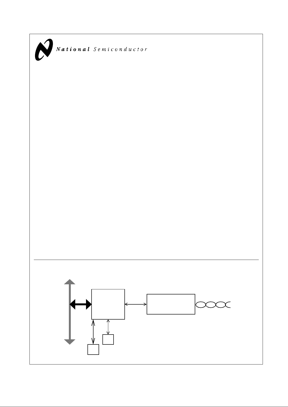
System Diagram
PCI Bus
DP83820
EEPROM (optional)
10/100/1000 Mb/s
PHY
Boot ROM (optional)
MII
GMII
Page 2

2
www.national.com
1.0 Connection Diagram
Order Number DP83820VUW
See NS Package Number NVUW208A
AD16
CBEN2
PCIVSS
FRAMEN
IRDYN
TRDYN
PCIVDD
DEVSELN
STOPN
PERRN
SERRN
PAR
CBEN1
AD15
AD14
PCIVSS
AD13
AD12
AD11
PCIVDD
AD10
AD9
AD8
CBEN0
AD7
AD6
PCIVSS
AD5
AD4
PCIVDD
AD3
AD2
AD1
AD0
ACK64N
PCIVSS
REQ64N
CBEN7
CBEN6
PCIVDD
CBEN5
CBEN4
PAR64
AD63
AD62
PCIVSS
AD61
AD60
AD59
AD58
PCIVDD
AD57
MD7
MD6
MD5
MD4/EEDO
VDDIO
VSSIO
MD3
MD2
MD1/CFGDISN
MD0/PMGDISN
MWRN
MRDN
MCSN
EESEL
RESERVED
COREVDD
COREVSS
CLKRUNN
3VAUX
PWRGOOD
PCIVIO
AD32
AD33
AD34
PCIVDD
AD35
AD36
AD37
PCIVSS
AD38
AD39
AD40
AD41
PCIVDD
AD42
AD43
AD44
AD45
PCIVSS
AD46
AD47
AD48
AD49
AD50
PCIVDD
AD51
AD52
AD53
PCIVSS
AD54
AD55
AD56
RXD0
RXD1
RXD2
RXD3
VSSIO
VDDIO
RXD4
RXD5
RXD6
RXD7
RXDV/RXD8
RXER/RXD9
CRS/SIG_DET
COL
RXEN
PHYRSTN
COREVSS
COREVDD
PMEN
PCICLK
TRSTN
TCK
TMS
TDO
TDI
PCIVSS
INTAN
RSTN
GNTN
REQN
PCIVDD
AD31
AD30
AD29
AD28
AD27
AD26
AD25
AD24
PCIVSS
CBEN3
IDSEL
AD23
AD22
PCIVDD
AD21
AD20
AD19
COREVSS
COREVDD
AD18
AD17
157
158
159
160
161
162
163
164
165
166
167
168
169
170
171
172
173
174
175
176
177
178
179
180
181
182
183
184
185
186
187
188
189
190
191
192
193
194
195
196
197
198
199
200
201
202
203
204
205
206
207
208
123456789101112131415161718192021222324252627282930313233343536373839404142434445464748495051
52
104
103
102
101
100
99
98
97
96
95
94
93
92
91
90
89
88
87
86
85
84
83
82
81
80
79
78
77
76
75
74
73
72
71
70
69
68
67
66
65
64
63
62
61
60
59
58
57
56
55
54
53
156
155
154
153
152
151
150
149
148
147
146
145
144
143
142
141
140
139
138
137
136
135
134
133
132
131
130
129
128
127
126
125
124
123
122
121
120
119
118
117
116
115
114
113
112
111
110
109
108
107
106
105
DP83820
Gigabit NIC
RXCLK/RXPMACLK1
TXCLK/RXPMACLK0
TXER/TXD9
TXEN/TXD8
TXD7/MA15
TXD6/MA14
VDDIO
VSSIO
TXD5/MA13
TXD4/MA12
TXD3/MA11
TXD2/MA10
VDDIO
VSSIO
TXD1/MA9
TXD0/MA8
GTXCLK/TXPMACLK
MDIO
MDC
REF125
VDDIO
VSSIO
SPD1000
SPD100
PHYLNK
GP1DUP
GP5
GP4
GP3
GP2
RESERVED
AVDD
AVSS
OSCVDDX1X2
OSCVSS
RESERVED
RESERVED
RESERVED
COREVDD
COREVSS
MA7
MA6
MA5
VDDIO
VSSIO
MA4/EECLK
MA3/EEDI
MA2
MA1
MA0
Page 3

3
www.national.com
2.0 Pin Descriptions
PCI In t e r f a c e
Symbol Pin No(s) Direction Descripti on
AD31-0 188, 189, 190 ,
191, 192, 193 ,
194, 195, 199 ,
200, 202, 203 ,
204, 207, 208 ,
1, 14, 15, 17,
18, 19, 21, 22,
23, 25, 26, 28,
29, 31, 32, 33,
34
I/O
Address and Data:
Multipl exed address an d da ta bus. As a bus ma s t er, the
DP83820 will drive address during the first bus phase. During subsequent
phases, the DP8 3820 will either read or write dat a exp ecting the target to
increment its address po inter. As a bus target, the DP83820 will decode each
address on the bus and respond if it is the target being addressed.
CBEN3-0 197, 2, 13, 24 I/O
Bus Command/Byte Enable:
During the address phase these signals define
the “bus command” or the type of bus tr an sac ti on t ha t wil l tak e pl ace . D uri ng the
data phase these pins in dicate which byte lanes contain valid data. CBEN0
applie s to byte 0 (bits 7-0) and C BEN3 applies to byte 3( bits 31-24).
PCICLK 176 I
Clock:
This PCI Bus clock provi des timing for all bus phases. The rising edge
defines the start of each phase. The cl ock frequency ranges from 0 to 66 MHz.
DEVSELN 8 I/O
Device Selec t:
As a target, the DP8382 0 asserts this signal low when it
recognizes its address after FRAMEN is asserted. As a bus master, the
DP83820 samples this signal to insure that the destination address for the data
transfer is recognized by a PCI target.
FRAMEN 4 I/O
Frame:
As a bus master, this signal is asserted low to indicate the beginning
and duration of a bus transac tion. Data transfe r takes place when this s ignal is
asserted. I t is de-asserted before th e transaction i s in its final phase. As a
target, the device monitors this signal before decoding the address to check if
the current transaction is addressed to it.
GNTN 185 I
Grant:
This signal is asserted low to indicate to the DP83820 that it has been
granted ownership of the bus by the central arbiter. This input is used when the
DP83820 is acting as a bus master.
IDSEL 198 I
Initialization Device Select:
This pin is sampled by the DP83820 to identify
when configuration read and write accesses are in tended for it.
INTAN 183 O
Interrupt A:
This signal is asserted low w hen an interrupt condition as defined
in the Interrupt Status Register, Interrupt Mask, and Interrupt Enable registers
occurs.
IRDYN 5 I/O
Initiator Ready:
As a bus master, this signal will be asserted low when the
DP83820 is ready to complete the current data phase transaction. This signal is
used in conjunction with the T RYDN signal. Data transaction ta kes place at t he
rising edge of PCICLK when both IRDY N and TRDYN are asserted low. As a
target, this signal indicates that the master has put the data on the bus.
PAR 12 I/O
Parity:
This sign al in di cate s even parity acr o ss AD 31 -0 an d CB EN 3-0 inc lu ding
the PAR pin. As a master, PAR is asserted during address and write data
phases. As a target, PAR is asserted during read data phases.
PERRN 10 I/O
Parity Error:
The DP83820 as a master or target will assert this signal low to
indica te a pa rity er ror on an y in com ing d at a (e xc ep t for special c ycl es ). As a bus
master, it will monitor this signal on all write operations (except for special
cycles).
REQN 186 O
Request:
The DP83 820 will assert this signal low to request the owner s hip of
the bus to the central arbiter.
RSTN 184 I
Reset:
When this signa l is asserted all outp uts of DP83820 will be tri-stated
and the device will be put into a known state.
Page 4

4
www.national.com
2.0 Pin Descr iptions
(Continued)
SERRN 11 I/O
System Error :
This signal is asserted low by DP83820 during address parity
errors and system errors if enabled.
STOPN 9 I/O
Stop:
This signal is asserted low by the target device to request the master
device to stop the current transaction.
TRDYN 6 I/O
Target Ready:
As a target, this signal will be asserted low when the (slave)
device is re ad y to complet e the cu r rent data ph as e tr an sa c tion. This sig na l is
used in co njunction with the IRDYN signal . Data transaction tak es place at the
rising edge of PCICLK when both IRDYN and TRDYN are asserted low. As a
master, this signal indicates that the target is ready for the data during write
operation and with the data during read operation.
PMEN 175 O
Power Management Event:
This signal is asserted low by DP83820 to indicate
that a power management event has occurred.
3VAUX 86 I
PCI Aux Voltage Sense:
This pin is used to sense the presence of a 3.3v
auxiliary supply in order to define the PME Support available.
This pi n pad has an internal weak pull down.
PWRGOOD 85 I
PCI bus power good:
Connected to PCI bus 3.3v power, this pin is used to
sense the presence of PCI bus power during the D3 power management st ate.
This pi n pad has an internal weak pull down.
CLKRUNN 87 I/O
Clockrun
: This signal is asserted low by DP83820 to indicate that a Clockrun
Event has occurred.
AD63-32 44, 45, 47, 48,
49, 50, 52, 53,
54, 55, 57, 58,
59, 61, 62, 63,
64, 65, 67, 68,
69, 70, 72, 73,
74, 75, 77, 78,
79, 81, 82, 83
I/O
64-bit Extension Address and Data:
Multiplexed addr ess and data bus.
Provides upper address bits during 64-bit DAC command. During data phase,
used for transferring upper 32-bits of a 64-bit data transaction.
CBEN7- 4 38, 39, 41, 42 I/O
64-bit Extension Bus Command/Byte Enables:
During the address phase
these signals define the “bus command” for a 64-bit DAC comman d. During a
64-bit data phase these pins indicate which byte lanes contain valid data.
CBEN4 applies to byte 4(bits 39-32) and CBEN7 applies to byte 7(bits 63-56).
REQ64N 37 I/O
Request 64-bit Transfer:
The DP83 820 will assert this signal low to request a
64-bit transfer of data. This pin is sampled by the DP83820 during reset to
determine if the device is connected to a 64-bit datapath.
ACK64N 35 I
Acknowledge 64-bit Transfer:
The DP83820 will samples this signal on bus
master cyc le s whe n i t h as re qu este d a 6 4-b it da ta transfer . If bo t h RE Q64 N and
ACK64N are asserted, the n a 64-bit transfer will be per formed. As a target, the
DP83820 only supports 32-bit transfers, so it will never assert ACK64N.
PAR64 43 I/O
Parity Upper DWORD:
This signal indicates even parity across AD63-32 and
CBEN7-4 including the PAR64 pin. As a master, PAR64 is driven during
address and write data phases. As a target, the DP83820 only supports 32-bit
transfers, so it will not drive PAR64.
PCIVIO 84 I
PCI Bu s VIO:
This pin should be connected to the VIO pins of the PCI bus. It
provides a direct connection to the ESDPLUS ring for biasing. It may be
connected to 5V if available. It should not be connected to 3.3V unless all
signal ing i s 3 .3 V as th is w ill in te rfere with 5V tol er anc e . C ar e s ho ul d be t aken in
connecting this to power supplies when power management functions are
enabled.
PCI In t e r f a c e
Symbol Pin No(s) Direction Descripti on
Page 5

5
www.national.com
2.0 Pin Descr iptions
(Continued)
Media Independent Interface (MII) - and Gigabit Media Independent Interface (GMII).
Symbol Pin No(s) Direction Description
COL 170 I
Collision Detect:
The COL signal is asserted high asynchronously by the
external PMD upon detection of a collision on the medium. It will remain
asserted as long as the collision condition persists.
CRS/SIGDET 169 I
Carrier Sense:
This signal is asserted high a synchronously by the external
physical un it up on dete c t io n of a non - id le med iu m .
Signal Dete ct:
In TBI mode , this signal is used to bring in the Signal Detect
indication from the Phy.
MDC 138 O
Management Data Clock:
Clock signal with a maximum rate of 2.5 MHz used
to transfer management data for the external PMD on the MDIO pin.
MDIO 139 I/O
Management Data I/O:
Bidirectional signal used to transfer management
information for the external PMD. Requires an external 4.7 KΩ pullup resistor.
RXCLK/
RXPMACLK1
156 I
Receive Clock:
A continuous clock, sourced by an external PMD device, that is
recovered from the incoming data. Duri ng 1000 Mb/s mode RX_C LK is 125
MHz, during 100 Mb/s operation RX_CLK i s 25 MHz and during 10 Mb/s this is
2.5 MHz.
Receive PMA Clock 1:
In TBI mode, this 62.5Mhz clock is used in conjunction
with RXP MA C LK0 to clo c k 10- b it TB I data in to the D P83 82 0. The r is in g edge of
RXPMAC LK1 clocks the even-numbered bytes .
RXD7,
RXD6,
RXD5,
RXD4,
RXD3,
RXD2,
RXD1,
RXD0
166,
165,
164,
163,
160,
159,
158,
157
I
Gigabit Receive Data:
This is a group of 8 signal s, sourced from an external
PMD, that contains data aligned on byte boundaries and are driven
synchronous to the RX_CLK. RXD7 is most signif icant bit.
Receive Data:
This is a group of 4 signals, sourced from an external PMD, that
contains data aligned on nibble boundaries and are driven synchronous to the
RX_CLK. RXD3 is the most significant bit and RXD0 is the least significant bit.
RXD7 through RXD4 are not used in this mode.
TBI Receive Data:
In TBI mode, these bits are the lower 8 bits of the 10-bit TBI
Receive data.
RXDV/RXD8 167 I
Receive Data Valid:
This indicates that the external PMD is presenting
recovered and decoded nibbles on the RXD signals, and that RX _CLK is
synchronous to the recovered data in 10 0 Mb/s operation. This signal will
encompass the frame, starting with the Start-of-Frame delimiter (JK) and
excluding any End-of-Frame delimiter (TR).
TBI Receive Data:
In TBI mode, this is RXD8 of the 10-bit TBI Receive data.
RXER/RXD9 168 I
Receive Error:
This signal is asserted high synchronously by the external PMD
whenever it detects a media error and RXDV is asserted in 100 Mb/s or 1000
Mb/s op era tion.
TBI Receive Data:
In TBI mode, this is RXD9 of the 10-bit TBI Receive data.
RXEN 171 O
Receive Output Enable:
This pin is used t o disable an external PMD while the
BIOS ROM is being accessed.
TXCLK/
RXPMACLK0
155 I
MII Transmit Clock:
A continuous clock that is sourced by the external PMD.
During 100 Mb/s operation this is 25 MHz +/- 100 ppm. During 10 Mb/s
operation this clock is 2.5 MHz +/- 100 ppm.
Receive PMA Clock 0:
In TBI mode, this 62.5Mhz clock is used in conjunction
with RXP MA C LK1 to clo c k 10- b it TB I data in to the D P83 82 0. The r is in g edge of
RXPMAC LK0 clocks the odd-numbered bytes.
Page 6

6
www.national.com
2.0 Pin Descr iptions
(Continued)
TXD7/MA15,
TXD6/MA14,
TXD5/MA13,
TXD4/MA12,
TXD3/MA11,
TXD2/MA10,
TXD1/MA9,
TXD0/MA8
152,
151,
148,
147,
146,
145,
142,
141
O
Gigabit Transmit Data:
This is a group of 8 signa ls which are driven
synchronous to GTXCLK. TXD7 is the most significant bit.
Transmit Data:
This is a group of 4 dat a signals which are driven synchronous
to the TXCLK for transmission to the external PMD. TXD3 is the most significant
bit and T XD0 is th e l east si gn i fica nt bi t. T X D7 t hro ug h T XD4 a r e no t use d i n th is
mode
TBI Transmit Data:
In TBI mode, this is the lower 8 bits of the 10-bit TBI
Transmit data.
BIOS ROM Address
: During external BIOS ROM access, these signals
become part of the RO M address.
TXEN/TXD8 153 O
Transmit Enab le:
This signal is synchronous to TXCLK and provides precise
framing for data carried on TXD3-0 for the external PMD. It is asserted when
TXD3- 0 co ntains valid da ta to be transmi tte d.
TBI Transmit Data:
In TBI mode, this is TXD8 of the 10-bit TBI Transmit data.
TXER/TXD9 154 O
Transmit Error:
This signal is synchronous to TXCLK and provides error
indications and also is used for 1000 Mb/s half-duplex carrier extension and
pack et b ur st ing fu nc ti ons . Th e DP838 20 wil l on ly as se rt thi s s ig nal i n 10 00 Mb/s
mode of operation.
TBI Transmit Data:
In TBI mode, this is TXD9 of the 10-bit TBI Transmit data.
GTXCLK/
TXPMACLK
140 O
GMII transmit Cl ock:
A continuous clock used for 1000 Mb/s. It is output to an
external PMD and is the reference clock for Tr ansmit GMII signaling. The clock
frequency is 125 MHz.
TBI Transmit Cl ock:
In TBI mode, this is the 125MHz transmit clock to an
external PMD and is the reference for Transmit TBI signaling.
REF125 137 I
125 MHz Reference Clock:
May be optionally connected to a 125 MHz
oscillator for 1000 Mb/s mode. If not used should be tied high.
BIOS ROM/Flash Interface
Symbol Pin No(s) Direction Description
MCSN 92 O
BIOS PROM/Flash Chip Select:
During a BIOS ROM/Flash access, this
signal is used to select the R OM device.
MD7, MD6,
MD5, MD4/EEDO,
MD3, MD2,
MD1/CFGDISN,
MD0/PMGDISN
104, 103,
102, 101,
98, 97,
96,
95,
I/O
BIOS ROM/Flash Data Bus:
During a BIOS ROM/Flash access these
signals are used to transfer data to or from the ROM/Flash device.
MD5:0 and MD7 pin p ads have an in ternal weak pull up.
MD6 pin pad has an internal weak pull down.
MA15/TXD7,
MA14/TXD6,
MA13/TXD5,
MA12/TXD4,
MA11/TXD3,
MA10/TXD2,
MA9/TXD1,
MA8/TXD0,
MA7, MA 6,
MA5, MA 4/EECLK ,
MA3/E ED I, MA 2,
MA1, MA 0
152,
151,
148,
147,
146,
145,
142,
141,
114, 113,
112, 109,
108, 107,
106, 105
O
BIOS ROM/Flash Address:
During a BIOS ROM/Flash access, these
signals are used to drive the ROM/Flash address.
Media Independent Interface (MII) - and Gigabit Media Independent Interface (GMII).
Symbol Pin No(s) Direction Description
Page 7

7
www.national.com
2.0 Pin Descr iptions
(Continued)
Note: DP83820 supports NM27LV010 for the R O M interface device.
MWRN 94 O
BIOS ROM/Flash Write:
During a BIOS ROM/Flash access, this signal is
used to e nable data to be written to the Flash devi ce.
MRDN 93 O
BIOS ROM/Flash Read:
During a BIOS ROM/Flash access, this signal is
used to e nable data to be r ead from the Fla s h device.
Clock Interface
Symbol Pin No(s) Direction Description
X1 122 I
Crystal/Oscillator Input:
This pin is the primary clock reference input for the
DP83820 IC and must be connected to a 25MHz 0.005% (50ppm) clock source.
The DP83820 device supports either an external crystal resonator connected
across pins X1 and X2, or an external CMOS-level oscillator source connected
to pin X1 only.
X2 121 O
Crystal Output:
This pin is us ed in conj u ncti on wit h t he X1 p in to c onnec t t o a n
external 25MHz crystal resonator device. This pin must be left unconnected if
an external CMOS oscillator clock source is utilized. For more information see
the definition for pin X1.
Phy And General Purpose Interface
Symbol Pin No(s) Direction Descripti on
GP1DUP 131 I/O
General Purpose Pin 1 or Duplex Status:
By default, this pin ca n be used to
input the Full Duplex status from an external Phy. The pin can also be
programmed as a general purpose I/O. This pin pad has an internal weak pull
up.
GP2 127 I/O
General Purpose Pin 2:
This pi n is a general purpose I/O pin that can be
programmed as an input or output. This pin has an internal weak pull up.
GP3 128 I/O
General Purpose Pin 3:
This pi n is a general purpose I/O pin that can be
programmed as an input or output. This pin has an internal weak pull up.
GP4 129 I/O
General Purpose Pin 4:
This pi n is a general purpose I/O pin that can be
programmed as an input or output. This pin has an internal weak pull up.
GP5 130 I/O
General Purpose Pin 5:
This pi n is a general purpose I/O pin that can be
programmed as an input or output. This pin has an internal weak pull up.
PHYLNK 132 I
Phy L i nk S ta tus :
This ca n be us ed to in pu t th e Ph y Li nk S tat u s. Thi s a ll o ws t he
valu e to be read back from the MAC register space.
SPD100 133 I
100 Mb/s Speed Status:
This can be used to in pu t t he 100 Mb/ s S pee d Sta tus
from an external phy. This is used along with the SPD1000 bit to determine
current speed status of the Phy.
SPD1000 134 I
1000 Mb/s Speed Status:
This can be used to input the 1000 Mb/s Speed
Status from an external phy. This is used along with the SPD100 bit to
determine cu r rent spee d st atus of the Phy.
PHYRSTN 172 O
Phy Re set:
This pin can be used to reset an External Ph y.
BIOS ROM/Flash Interface
Symbol Pin No(s) Direction Description
Page 8

8
www.national.com
2.0 Pin Descr iptions
(Continued)
Note: DP83820 supports NMC93C46 for the eeprom interface device.
Serial EEPROM Interface
Symbol Pin No(s) Direction Description
EESEL 91 O
EEPROM Chip Select:
This signal is used to enable the external EEPROM
device.
MA4/EECLK 109 O
EEPROM Clock:
During an EEPROM access (EESEL asserted), this pin is an
output used to drive the serial clock to an external EEPROM device.
MA3/EEDI 108 O
EEPROM Data In:
During an EEPROM access (EESEL asse r t ed ), this outpu t
is drives opcode, address, and data to an external serial EEPROM device.
MD4/EEDO 101 I
EEPROM Data Out:
During an EEPROM access (EESEL asserted), this pin is
an input used to retrieve EEPROM serial read data.
This pi n pad has an internal weak pull up.
JTAG Interface
Symbol Pin No(s) Direction Description
TCK 178 I Test Clock
TDI 181 I Test Data Input
TDO 180 O Test Output
TMS 179 I Test Mode Select
TRSTN 177 I Test Reset
Supply Pins
Symbol Pin No(s ) Direction Description
COREVD D 89, 116, 174, 206 S Mac/BIU digital core VDD - connect to Aux 1.8V supply VDD
COREVSS 88, 115, 173, 205 S Mac/BIU digital core VSS.
OSCVDD 123 S Oscillator VDD - connect to Aux 1.8V supply VDD
OSCVSS 120 S Oscillator VSS.
PCIVDD 187 , 201, 7, 20 , 30,
40, 51, 60, 71, 80
S PCI IO VDD - connect to PCI bus 3.3V VDD
PCIVSS 182, 196, 3, 16, 27,
36, 46, 56, 66, 76
S PCI IO VSS
VDDIO,
AVDD
100, 111, 136, 144,
150, 162, 12 5
S Misc. IO VD D, Analog VDD - connect to Aux 3.3V supply VDD
VSSIO,
AVSS
99, 110, 135, 143,
149, 161, 12 4
S Misc. IO VSS, Analog VSS
No Connects
Symbol Pin No(s) Direction Description
Reserved 90, 117, 118,
119, 126
This pin is reserved and cannot be connected to any external logic or net.
Page 9
9
www.national.com
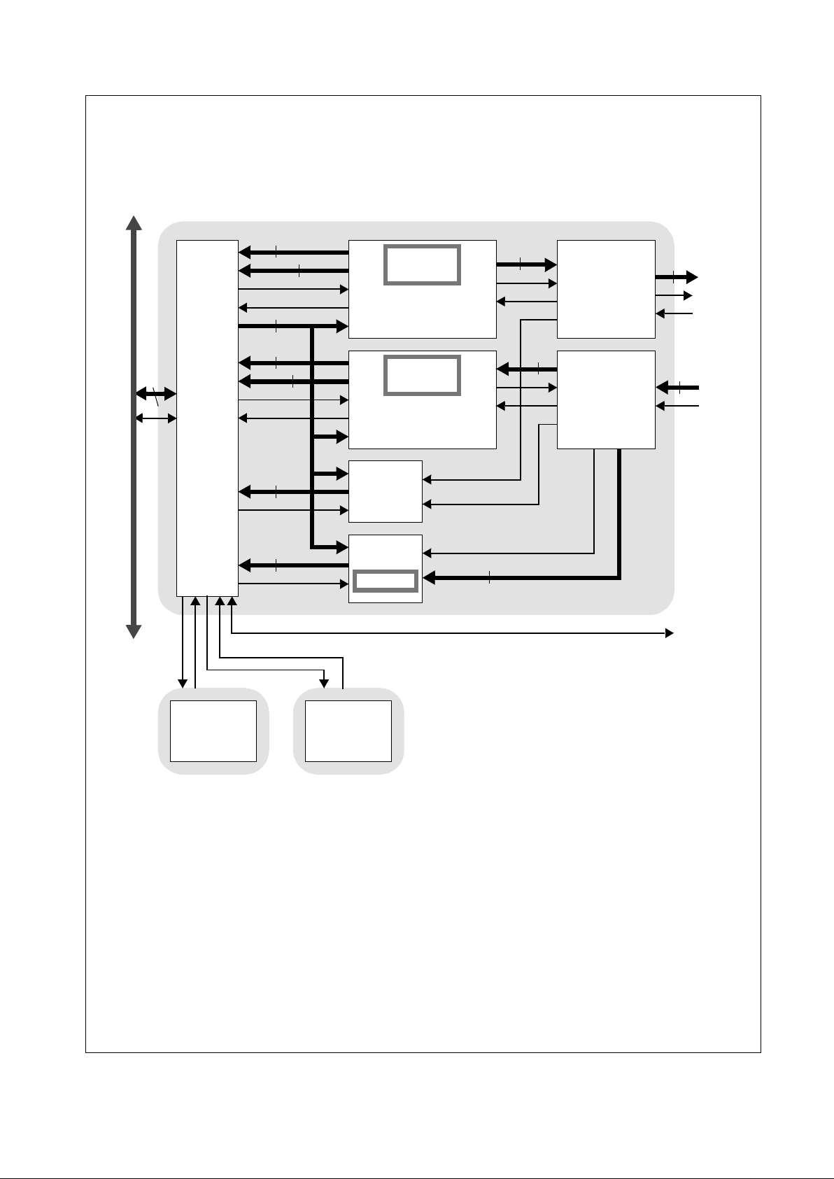
3.0 Functional Description
DP83820 consists of a PCI bus interface, BIOS ROM and
EEPROM interfaces, Receive and Transmit Data Buffer
Managers, an 802.3 Media Access Controller (MAC),
SRAM, and miscellaneous support logic.
Figure 3-1
DP83820
Functional Block Diagram
3.1 DP83820
The DP83820 device is an enhanced version of the NSC
MacPhyter MAC/BIU (Media Access Controller/Bus
Interface Unit) which has been modified for 1000 Mb/s
operation with additional buffering, higher bandwidth PCI
bus implementation, and the Gigabit Media Independent
Interface for 1000BASE-T phy support. The DP83820
supports an exter nal 10/100/1000 physical layer device.
DP83820 contains the following major design elements:
— a PCI bus interface,
— an EEPROM interface, for access to an NMC93C06
EEPROM,
— a buffer management scheme that is simple, efficient
and flexible,
— separate receive and transmit FIFOs and DMA
controllers,
— a 10/100/1000 Mb/s Ethernet Media Access Control
(MAC),
— a Physical Layer Interface (MII/GMII/TBI ),
— Management Information Base (MIB) Statistics
Registers,
— Receive Packet filteri ng logic.
This following section provides a functional overview of
interfaces of the DP83820.
Rx Filter
Tx Buffer Manager
Rx Buffer Manager
MIB
Tx MAC
Rx MAC
PCI BUS
PCI Bus
Interface
Data FIFO
Data FIFO
93C06
Serial
EEPROM
DP83820
32
15
64
32
64
32
32
64
64
64
8
8
64
Boot ROM/
Flash
MII
MGMT
SRAM
G/MII INTERFACE
Page 10

3.0 Functional Description
(Continued)
10
www.national.com
3.2 PCI Bus Interface
The DP83820 implements the Peripheral Component
Interconnect (PCI) bus interface as defined in PCI Local
Bus Specification Version 2.2. When internal register are
being accessed the DP83820 acts as a PCI target (slave).
When accessin g host memory for descriptor or packet data
transfer, the DP83820 acts as a PCI bus master.
All required pins and functions are implemented. The
optional interface pin INTA for support of interrupt requests
is implemented as well . The b us inte rf ace also supports 64bit and 66Mhz operation in addition t o the more common
32-bit and 33-Mhz capabilities.
For more information, refer to the PCI Local Bus
Specification version 2.2, December 18, 1998.
3.2.1 Byte Ordering
The DP83820 can be configur ed to order the bytes of data
on the AD[31:0] bus to conform to Little Endian or Big
Endian ordering through the use of the CFG:BEM bit. Byte
ordering only affects bus mastered packet data transfers in
32-bit mode. Register infor mation remains bit aligned (i.e.
AD[31] maps to bi t 31 in any register space, AD[0] maps to
bit 0, etc.) when registers are accessed with 32-bit
operations. Bus mastered transfers of buffer descriptor
information also remain bit aligned.
When configured for Little Endian (CFG:BEM=0), the byte
orientation for receive and transmit data and descriptors in
sys tem memory i s as follows:
Figure 3-2 Little Endi an Byte Ordering
When configured for big-endian mode (CFG:BEM=1), the
byte orientation for receive and transmit data and
descriptors in system memory is as follows:
Figure 3-3 Big Endian Byte Ordering
3.2.2 Interrupt Control
Interrupts are performed by asynchronously asser ting the
INTAN pin. This pin is an open drain output. The source of
the interrupt can be determined by reading the Interrupt
Status Register (ISR) (See Section 4.2.6). One or more
bits in the ISR will be set, denoting all currently pending
interrupts. Reading of the ISR clears ALL bits. Masking of
specific interrupts can be accomplished by using the
Interrupt Mask Register (IMR) (See Section 4.2.7).
Assertion of INTAN can be prevented by clearing the
Interrupt Enable bit in the Interrupt Enable Register (See
Section 4.2.8). This allows the system to defer interrupt
processing as needed.
3.2.3 Latency Timer
The Latency Timer described in CFGLAT:LAT (See Section
4.1.4) defines the maximum number of bus clocks that the
device wil l hold the bus. Once the device gains control of
the bus and issues FRAMEN, the Latency Timer will begin
counting down. If GNTN is deasserted before the DP83 820
has finished with the bus, the device will maintain
ownership of the bus until the timer reaches zero (or has
finished the bus transfer). The timer i s an 8-bit counter, with
the lower 4 bits hard-coded to 1111b. This means that the
timer val ue can only be incremented in units of 16 clocks.
3.2.4 64-Bit Data Operation
The DP83820 supports 64-bit operat ion as a bus master
for transferring descriptor and packet data information. This
mode can be enabled or disabled through configuration
from EEPROM. As a target, the DP83820 only supports
32-bit mode of operation. At the rising edge of RSTN, the
DP83820 samples the REQ64N pin to determine if the bus
is 64-bit capable. If the bus is not 64-bit capable, the
DP83820 will drive the 64-bit extension signals AD[63:32],
CBEN[7:4], and PAR64 to a low level to prevent the fl oating
inputs from causi ng significant current drain.
3.2.5 64-Bit Addressing
The DP83820 supports 64-bit addressing (Dual Address
Cycle) as a bus master for transferring descriptor and
packet data information. This mode can be enabled or
disabled through configuration from EEPROM. The
DP83820 also supports 64-bit addr essing as a target.
3.3 Bus Operation
3.3.1 Target Read
A Target Read operation starts with the system generating
FRAMEN, Address, and either an IO read (0010b) or
Memory Read (0110b) command. See Figure 3-4. If the
32-bit address on the address bus matches the IO address
range specified in CFGIOA:IOBASE (for I /O reads) or the
memory address range specified in CFGMA:MEMBASE
(for memory reads), the DP83820 will generate DEVSELN
2 clock cycles later (medium speed).
The system must tri-state the Address bus, and convert the
C/BEN bus to byt e enables, after the address cycl e. On the
2nd cycle after the assertion of DEVSELN, all 32-bits of
data and TRDYN will become valid. If IRDYN is asserted at
that time, TRDYN will be forced HIGH on the next clock for
1 cycle, and then tri-stated.
Byte 3Byte 2Byte 1Byte 0
31 24 23 16 15 8 7 0
(MSB)
(LSB)
C/BEN[3] C/BEN[2] C/BEN[1] C/BEN[ 0]
Byte 0Byte 1Byte 2Byte 3
31 24 23 16 15 8 7 0
(LSB)
(MSB)
C/BEN[3] C/BEN[2] C/BEN[1] C/BEN[ 0]
Page 11
3.0 Functional Description
(Continued)
11
www.national.com
If FRAMEN is asserted beyond the assertion of IRDYN, the
DP83820 will still make data available as descri bed above,
but will also issue a Disconnect. That is, it will assert the
STOPN signal with TRDYN. STOPN will remain as serted
until FRAMEN is detected as deass erted.
Figure 3-4 Target Read Operation
3.3.2 Target Writ e
A Target Write operation starts with the system generating
FRAMEN, Address, and Command (0011b or 0111b). See
Figure 3-5. If the upper 24 bi ts on the address bus match
CFGIOA:IOBASE (for I/O reads) or CFGMA:MEMBASE
(for memory reads), the DP83820 will generate DEVSELN
2 clock cycles later.
On the 2nd cycle after the assertion of DEVSELN, the
device will monitor the IRDYN signal. If IRDYN is asserted
at that time, the DP83810 will assert TRDYN. On the next
clock the 32-bit double word will be latched in, and TRDYN
will be forced HIGH for 1 cycle and then tri-stated.
Note: Target write operations must be 32-bits wide.
If FRAMEN is asserted beyond the assertion of IRDYN, the
DP83820 will still la tch the fi rst double word as descr ibed
above , but will also i ssue a Disconnect. That is, it will assert
the STOPN signal with TRDYN. STOPN will remain
asserted until FRAMEN is detected as deasserted.
Figure 3-5 Target Write Operation
Addr
Data
CLK
FRAMEN
AD[31:0]
C/BEN[3:0]
IRDYN
TRDYN
DEVSELN
PAR
PERRN
Addr Data
CLK
FRAMEN
AD[31:0]
C/BEN[3:0]
IRD YN
TRDYN
DEVSELN
PAR
PERRN
Page 12

3.0 Functional Description
(Continued)
12
www.national.com
3.3.3 Master Read
A Master Read operation starts with the DP83820
asserting REQN. See Figure 3-6. If GNTN is asserted
within 2 clock cycles, FRAMEN, Address, and Command
will be generated 2 clocks after REQN (Address and
FRAMEN for 1 cycle only). If GNTN is asserted 3 cycles or
later, FRAM EN, Address, and Command will be generated
on the clock following GNTN.
The device will wait for 8 cycles for the assertion of
DEVSELN. After 8 clocks without DEVSELN, the device
will issue a Master Abort by asserting FRAM EN HIGH for 1
cycle. IRDYN will be forced HIGH on the following cycle.
Both signals will become tri-state on the cycle following
their deassertion.
On the clock edge after the generation of Address and
Command, the address bus will become tri-state, and the
C/BEN bus will contain valid byte enables. On the clock
edge after FRAMEN was asserted, IRDYN will be asserted
(and FR AMEN will be deasserted if this is to be a single
read operation). On the clock where both TRDYN and
DEVSELN are detected as as serted, data will be latched in
(and the byte enables will change if necessary). This will
continue until the cycle following the deassertion of
FRAMEN.
On the clock where the second to last read cycle occurs,
FRAMEN will be forced HIGH (it will be tri-stated 1 cycle
later). On the next clock edge that the device detects
TRDYN asser ted, it will force IRDYN HIGH. It, t oo, will be
tri-stated 1 cycle later. This will conclude the read
operation. The DP83820 will never f orce a wait state during
a read operation.
Figure 3-6 Master Read Operat ion
3.3.4 Master Writ e
A Master Write operation starts with the DP83820
asserting REQN. See Figure 3-7. If GNTN is asserted
within 2 clock cycles, FRAMEN, Address, and Command
will be generated 2 clocks after REQN (Address and
FRAMEN for 1 cycle only). If GNTN is asserted 3 cycles or
later, FRAM EN, Address, and Command will be generated
on the clock following GNTN.
The device will wait for 8 cycles for the assertion of
DEVSELN. After 8 clocks without DEVSELN, the device
will issue a Master Abort by asserting FRAM EN HIGH for 1
cycle. IRDYN will be forced HIGH on the following cycle.
Both signals will become tri-state on the cycle following
their deassertion.
On the clock edge after the generation of Address and
Command, the data bus will become valid, and the C/BEN
bus will contain valid byte enables. On the clock edge after
FRAMEN was asserted, IRDYN will be asserted (and
FRAMEN will be deasserted if this is to be a single read
operation). On the clock where both TRDYN and
DEVSELN are detected as asserted, valid data for the next
cycle will become available (and the byte enables will
change if necessary). This will continue until the cycle
following the deassertion of FRAMEN.
On the clock where the second to last write cycle occurs,
FRAMEN will be forced HIGH (it will be tri-stated 1 cycle
later). On the next clock edge that the device detects
TRDYN asser ted, it will force IRDYN HIGH. It, t oo, will be
tri-stated 1 cycle later. This will conclude the write
operation. The DP83820 will never f orce a wait state during
a write operati on.
Addr
Data
CLK
FRAMEN
AD[31:0]
C/BEN[3:0]
REQN
GNTN
IRD YN
TRDYN
DEVSELN
PAR
Page 13

3.0 Functional Description
(Continued)
13
www.national.com
Figure 3-7 Master Write Operation
3.3.5 Configurati on Access
Configuration register accesses are similar to Target reads
and writes in that they are singl e data word transfer s and
are initiated by the system. For the system to initiate a
Configuration access, it must also generate IDSELN as
well as the correct Command (1010b or 1011b) during the
Address phase. The DP83820 will respond as it does
during Target operations.
Note: Configuration reads must be 32-bits wide, but writes may access individual
bytes.
3.4 Packet Buffering
The DP83820 incorporates two independent FIFOs for
transferring data to/from the system interface and from/to
the network. The FIFOs, providing temporary storage of
data, free the host system from the real-time demands of
the network.
The way in which the FIFOs are emptied and filled is
controlled by the FIFO threshold values in the TXCFG and
RXCFG registers (See Sections 4.2.12 and 4.2.16). These
values determine how full or empty the FIFOs must be
before the device requests the bus. Additionally, there is a
threshold value that determines how f ull the transmit FIFO
must be before beginning tr ansm ission. Once the DP83820
requests th e bus, it will attempt to empty or fill the FIFOs as
allowed by the respective MXDMA settings in TXCFG and
RXCFG.
3.4.1 Transmit Buf fer Manager
The buffer management scheme used on the DP83820
allows quick, simple and efficient use of the frame buffer
memory. The buffer management scheme uses separate
buffers and descriptors for packet infor mation. This allows
effective transfers of data to the transmit buffer manager by
simply transferring the descriptor information to the
transmit queue. Refer to the Buffer Management section for
complete information.
The Tx Buffer Manager DMAs packet data from PCI
memory space and places it in the 8KB transmit FI FO, and
pulls data from the FIFO to send to the Tx MAC. Multiple
packets may be present in the FIFO , allowing packets to be
transmitted with minimum int erframe gap. The way in which
the FIFO is emptied and filled is controlled by the FIFO
threshold values in the TXCFG register: FLTH (Tx Fill
Threshold), and DRTH (Tx Drain Threshold). Additionally,
once the DP83820 requests the bus, i t will attempt to fill the
FIFO as allowed by the MXDMA setting in the TXCFG
register.
3.4.2 Transmit Priority Queueing
The Tx Buffer Manager process also supports priority
queueing of transmit packets. It handles this by drawing
from four separ ate descriptor lists to fill the internal FIFO . If
packets are available in the higher priority queues, they will
be loaded into the FIFO before those of lower priority.
3.4.3 Receive Buffer Manager
The Rx Buffer Manager uses the sam e buffer management
scheme as used for transmits. Refer to the Buffer
Management section for complete information.
The Rx Buffer Manager retrieves packet data from the Rx
MAC and places it in the 32KB receiv e dat a FIFO , and pulls
data from the FIFO for DMA to PCI memory space. The Rx
Buffer Manager maintains a status FIFO, allowing up to 32
packets to reside in the FIFO at once. Similar to the
transmit FIFO, the receive FIFO is controlled by the FIFO
threshold value in RXCFG:DRTH (Rx Drain Threshold).
This value determines the number of long words wr itten
into the FIFO from the MAC unit before a DMA request for
system memory occurs. Once the DP83820 gets the bus, it
will continue to transfer the long words from the FIFO until
the data in the FIFO is less than one long word, or has
reached the end of the packet, or the max DMA burst size
is reached (RXCFG register:MXDMA).
3.4.4 Receive Priorit y Que ueing
The Rx Buffer Manager process also supports priority
queueing of receive packets. It handles this by placing
packets on up to four separate descriptor lists when
emptying the inter nal FIFO. The Rx Buffer Manager uses
information in a VLAN tag to determine packet priority.
Addr
Data
CLK
FRAMEN
AD[31:0]
C/BEN[3:0]
REQN
GNTN
IRD YN
TRDYN
DEVSELN
PAR
Page 14

3.0 Functional Description
(Continued)
14
www.national.com
3.4.5 Packet Recognition
The Receive packet filter and recognition logic allows
software to control which packets are accepted based on
destination address and packet type. Address recognition
logic includes suppor t for broadcast, multicast hash, and
unicast addresses. The packet recognition logic includes
support for WOL, Pause, and programmable pattern
recognition.
3.5 Ethernet Media Access Controller (MAC)
The Media Access Control (MAC) unit perform s the control
functions for the media ac cess of transmitting and receiving
packets. During transmission, the MAC unit handles
building of frames and tr ansmission of the frames over the
interface to the physical layer device. During reception,
data is received from the physical layer interface, the frame
is checked for v alid reception, and the data is trans ferred to
the receive FIFO. Control and status registers in the
DP83820 gover n the operation of the MAC unit.
The standard 802.3 Ethernet packet consists of the
following fields: preamble, start of frame delimiter (SFD),
destination address, source address, length, data, frame
check sequence (FCS) and Extension (See Fi gure 3-8). All
fields are of fixed length except for the data field and
Extension. The Extension field is only used for 1000 Mb/s
half-duplex operation. During recepti on, the preamble and
SFD are stripped from the incoming packet. During
transmission, the DP83820 generates and prepends the
preamble and SFD. The FCS is normally appended by the
DP83820, but software may disable FCS inclusion on a
per-packet basis.
Figure 3-8 IEEE 802.3 Packet Structur e
3.5.1 Full Duplex Operation
Full duplex operation i s the simultaneous transmission and
reception of packet data. In t his mode of operation, r eceive
activity (CRS) is ignored in the decision making process for
transmissi on. During reception, collisions are al so ignored.
To configure the DP83820 to operate in full duplex, set
TXCFG:CSI
and
TXCFG:HBI=1
, and
RXCFG:RX_FD
= 1.
3.5.2 Full Duplex Flow Control
The DP83820 supports full duplex flow control using the
MAC Control Pause Frame as defined in the 802.3
specification. The packet recognition logic can detect
Pause frames, and cause the transmit MAC to pause the
correct number of slot times. In addition, the MAC can be
programmed to send Pause frames based on Rx FIFO
thresholds.
Flow Control operation is controlled by the Pause
Control/Stat us Register .
3.5.3 1000 Mb/s Operati on
The DP83820 includes additional features to support 1000
Mb/s speed of operation. In this mode, the physical layer
interface is increased from 4-bit MII to 8-bit GMII (or 10-bit
TBI). In addition, features such as carrier extension and
frame burst ing are required to meet the 802.3 specification
for 1000 Mb/s half-duplex operation.
3.6 Transmit MAC
The Transmit MAC implements the transmit portion of
802.3 Media Access Control. The Tx MAC retrieves packet
data from the Tx Buffer Manager and sends it out through
the transmit physical layer interface. Additionally, the Tx
MAC provides MIB control information for transmit packets.
The TX MAC supports 4-bit MII, 8-bit GMII, and 10-bit TBI
interf aces to physical layer devices
3.6.1 VLAN Tag Insertion
The Tx MAC has the capability to insert a 4-byte VLAN tag
in the transmit packet. If Tx VLAN Tag insertion is enabled,
the MAC will insert the 4 bytes, as specified in the VTAG
register, following the source and destination addresses of
the packet. The VLAN tag insertion can be enabled on a
global or per-packet basis.
3.6.2 Carrier Extension
For 1000 Mb/s half-duplex operation it is necessary for
MAC to ensure that all valid carrier events exceed a
slotTime of 4096 bit ti me s. To accomplish this, any transmit
event that is shorter than the slotTime will be extended
using Carrier Extension. On the GMII interface, this is
signaled to the Phy by TXER asserted with TXEN
deasserted and a TXD value of 0x0F.
3.6.3 Frame Bursting
The Tx MAC supports burst mode operation for 1000 Mb/s
half-duplex operation. This allows the device to transmit a
burst of packets without releasing control of the physical
medium. After a successful transmission, if additional
packets are available, the MAC will transmit a burst of
packets wi thout allowing the medium to go idle. It does thi s
by inserting carrier extension between the frames. The
MAC will continue to burst frames as long as additional
packets are available in the internal FIFO and a burstLimit
of 65536 bit times has not been exceeded.
3.6.4 IP Checksum Generation
The Tx MAC supports task offloading of IP, TCP, and UDP
checksum generation. It can generate the checksums and
insert them into the packet. The checksum generation can
be enabled on a global or per- packet basis.
3.7 Receive MAC
This block implements the receive portion of 802.3 Media
Access Control. The Rx MAC retrieves packet data from
the receive portion and sends it to the Rx Buffer Manager.
Additionally, the Rx MAC provides MIB control information
and packet address data for the Rx Filter. The RX MAC
supports 4-bit MII, 8-bit GMII, and 10-bit TBI interfaces to
physical layer devices.
preambl e S FD dest ad dr src addr le n
data
fcs
7 bytes 1 byte 6 bytes 6 bytes 2 bytes
46 to 1500 bytes 4 byte s
extension
<512 bytes
Page 15

3.0 Functional Description
(Continued)
15
www.national.com
3.7.1 VLAN Tag Handling
The Rx MAC can detect packets containing a 4-byte VLAN
tag, and remove the VLAN tag from the received packet. If
RX VLAN Tag removal is enabled, then the 4 bytes
following the source and destination addresses will be
stripped out. The VLAN status can be returned in the
Receive Descriptor Extended Status field.
3.7.2 Carrier Extension and Packet Bursting
The Receive MAC supports reception of packets with
Carrier Extension and packets transmitted using Frame
Bursting for 1000 Mb/s half-duplex operation. The first
frame in a burs t must be at least one slotTime in length,
otherwise it will be considered to be a collision fragment.
3.7.3 IP Checksum Verification
The Rx MAC supports IP checksum verification. It can
validate IP checksums as well as TCP and UDP
checksums. Packets can be discarded based on detecting
checksum errors.
3.8 P hysical L ayer Interface
The DP83820 implements a physical layer interface that
can support all of the following:
— Media Independent Interface (MII)
— Gigabit Media Independent Interface (GMII)
— Ten-Bit Interface (TBI)
In addition, the DP83820 implements a Management
interf ace as defined for MII and GMII.
3.8.1 Media Independ ent Interface (MII)
The DP83820 supports 10 Mb/s and 100 Mb/s physical
layer devices through the Media Independent Interface
(MII) as defined in IEEE 802.3 (clause 22). The MII
consists of a transmit data interface (TXEN, TXER,
TXD[3:0], and TXCLK), a receive data interface (RXDV,
RXER, RXD[3:0], and RXCLK), 2 status signals (CRS and
COL) and a management inter face (MDC and MDIO). In
this mode of operation, both Transmit and Receive clocks
are supplied by the Phy.
3.8.2 Gigabit Media Independ ent I nterface (GMII)
The DP83820 can support 1000 Mb/s physical layer
devices thr ough the Gigabit Media Independent Interface
(GMII) as defined in I EEE 802.3 (cl ause 35). The GMII is
extended from the MII to use 8-bit data interfaces and to
operate at higher frequency. The GMII consists of a
transmit data interface (TXEN, TXER, TXD[7:0], and
GTXCLK), a receive data interface (RXDV, RXER,
RXD[7:0], and RXCLK), 2 status signals (CRS and COL)
and a management interface (MDC and MDIO). Many of
the signals are shared with the MII interface. One
significant difference is the Transmit clock (GTXCLK) is
supplied by the DP83820 instead of the Phy. The
management interface (described later) is the same in both
MII and GMII modes
3.8.3 Ten-Bit Interface (TBI)
The TBI provides a port for transmit and receive data for
interfacing to devices that support the 1000Base-X portion
of the 802.3 specifi cation. This includes 1000Base-FX fiber
devices. The por t consists of data paths that are 10-bits
wide in each direction as well as control signals. This
interface shares pins with the MII and GMII interfaces.
3.8.4 MII/GMII Management Interface
The MII/GMII management interface utilizes a
communication protocol similar to a serial EEPROM.
Signaling occurs on two signals: clock (MDC) and data
(MDIO). This protocol provides capability for addressing up
to 32 individual Physical Media Dependent (PMD) devices
which share the same serial interface, and for addressing
up to 32 16-bit read/wr ite registers within each PMD. The
MII management protocol utilizes following frame format:
start bits (SB), opcode (OP), PMD address (PA), register
address (RA), line turnaround (LT) and data (See Figure 3-
9).
Figure 3-9 MII Management Frame Format
— Start bits are define d as <01>.
— Opcode bits are defined as <01> for a Write access and
<10> for a Read access.
— PMD address is the device addr ess.
— Register address is address of the register within that
device.
— Line turnaround bits wil l be <10> for Write acces ses and
will be <xx> for Read accesses. This allows time for the
MII lines to “turn around”.
— Data is the 16 bits of data that will be written to or read
from the PMD device.
A reset frame is also provided and defined as 32
consecutive 1s (FFFF FFFFh). After power up, all MII PMD
devices must wait for a reset frame to be received prior to
participating in MII management communication.
Additionally, a reset frame may be issued at any time to
allow all connected PMDs to re-synchronize to the data
traffic.
The MII/EEPROM Access Register (MEAR) is used to
provide access to the serial MII.
Refer to Section 4. 2.3 for compl ete details of the MEAR.
2b
2b 5b 5b 2b 16b
SB OP
PA RA
LT
Data
Note: b = bits
Page 16

3.0 Functional Description
(Continued)
16
www.national.com
3.9 EEPROM Inte rface
The DP83820 supports the attachment of an external
EEPROM. The EEPROM int erface provides the ability for
the DP83820 to read from and write data to an external
serial EEPROM device. Values in the external EEPROM
allow default fields in PCI configuration space and I/O
space to be overridden following a hardware reset. The
DP83820 will "autoload" v alues from the EEPROM to these
fields in configuration space and I/O space and perform a
checksum to verify that the data is valid. If the EEPROM is
not present, the DP83820 initialization uses default values
for the appropriate Configuration and Operational
Registers. Software can read and write to the EEPROM
using “bit-bang” accesses via the MII/EEPROM Access
Register (MEAR).
3.10 Boot ROM Interface
The BIOS ROM interface allows the DP83820 to read from
and writ e d at a to an external PROM /F la s h device.
3.11 Power Managemen t and Wake Functions
The DP83820 is compliant with the PCI Power
Management Specification v1.1. The device can be
programmed to any of the powered states (D0, D1, D2,
D3hot) and enabled to assert its PMEN pin through the
Configuration Register PMCSR. In addition, the device will
enter the D3cold state when PCI power is dropped,
regardless of the programmed power state. In either D3hot
or D3cold, if PMEN assertion is enabled, the device will
keep the receiver alive so that it may recognize wake
packets and signal the system to wake up; if PMEN
assertion is not enabl ed, the device will go to sleep and be
unable to rec eive packets.
The DP83820 supports several types of wake events that
will signal the power management logic to assert PMEN.
These are detailed in the Wake On LAN section (4.2.18.1).
In order for the device to request a system wake, at least
one wake e vent must be configured in the Wake Command
and Status Register (WCSR). If PMEN assertion i s enabled
and the device enters the D3cold state with no wake events
enabled, the device will go to sleep.
When the device is in a power management state other
than D0 (the fully alive state), the only PCI bus activity it
may initiate is the assertion of PMEN. This means any
packets received will remain in the receive FIFO until the
device is returned to the fully alive state. Upon waking up,
the wake packet is availab le i n the receive FIFO.
In any power state, enabling PMEN assertion adds
additional packet filtering: only those packet types that are
configured as wake packets in WCSR will be accepted.
This prevents non-wake packets from filling the receive
FIFO while the device is in a low power state and
preventing a wake packet from being accepted. It is
expected that while in the fully alive state, PMEN assertion
will be disabled to eliminate the extra level of filtering.
3.12 Network Management Fu nct i ons
The DP83820 allows compliance with several layer
management standards to allow a node to monitor overall
network perf ormance. These standards are:
— RFC 1213 (MIB II),
— RFC 1643 (Ether-like MIB), and
— IEEE 802.2 Layer Management.
Many of the counters required by these standards are
easily maintained in software during normal per-packet
processing. Those counters that would either be difficult or
impossible for software to maintain are provided for in
hardware (See Section 4.2.27). The table below outlines
each required counter, the relevant standard, and how the
counter should be maintained.
Table 3-1 MIB Compliance
Counter Name Reference Maintained by Derivation
RXOctetsOK RFC 1213,
802.3 LM
softw are, ad d cmdsts .SIZE on
receive packets with
cmdsts.OK bit set.
The byte count of each successfully
received packet is added to this counter.
The pac ket byte co un t in cl ud es the ad dres s ,
type, data, and FCS fields.
RXFramesOK 802.3 LM software, increment on
receive packets with
cmdsts.OK bit set.
This coun t er is in cr em ente d for each pack et
successfully received (this includes
broadcast, multicast, and physical address
packets).
RXBroadcastPkts RFC 1213,
802.3 LM
software, increment on
receive packets with
cmdsts.OK set and
cmdsts.DEST set to 11.
This counter is incremented for each
broadcast packet successfully received.
RXMulticastPkts RFC 1213,
802.3 LM
software, increment on
receive packets with
cmdsts.OK set and
cmdsts.DEST set to 10.
This counter is incremented for each
multicast packet successfully received.
RXErroredPkts RFC 1213 hardware, see
MIB:RxErroredPkts.
This coun t er is in cr em ente d for each pack et
received with errors. This count includes
packets which are automatically rejected
from the FIFO due to both wire errors and
FIFO overruns.
Page 17

3.0 Functional Description
(Continued)
17
www.national.com
RXFCSErrors RFC 1643,
802.3 LM
hardware, see
MIB:RXFCSErrors.
This coun t er is in cr em ente d for each pack et
received wit h a Frame Check Seque nc e
error (bad CRC).
RXMsdPktErrors RF C 1213, RFC
1643, 802.3 LM
hardware, see
MIB:RXMsdPktErrors.
This counter is incremented for each
receive aborted due to data or status FIFO
overruns (insuff icient buffer space).
RXFAEErrors RFC 1643,
802.3 LM
hardware, see
MIB:RXFAEErrors.
This coun t er is in cr em ente d for each pack et
received with a Frame Alignment error.
RXSymbolErrors 802.3 LM hardware, see
MIB:RXSymbolErrors
This coun t er is in cr em ente d for each pack et
received with one or more 100 Mb symbol
errors detected.
RXFrameTooLong RFC 1643,
802.3 LM
hardware, see
MIB:RXFrameTooLong.
This coun t er is in cr em ente d for each pack et
received with greater than the 802.3
standard maximum length of 1518 bytes.
RXIRLErrors 802.3 LM hardware, see
MIB:RXIRLErrors.
Packets received with In Range Length
errors. This counter increments fo r packets
received with a MAC length/type value
between 64 and 1518 bytes, inclusive, that
does no t match the number of bytes
received. This counter also increments for
packets with a MAC length/type field of less
than 64 bytes and more than 64 bytes
received.
RXBadOpcodes 802.3 LM hardware, see
MIB:RXBadOpcodes.
Packets received with a valid MAC control
type and an opcode for a function that is not
supported by the device
RXPauseFrames 802.3 LM hardware, see
MIB:RXPauseFrames.
MAC co ntrol Pause frames received.
TXOctetsOK RFC 1213,
802.3 LM
software, add sum of
cmdsts.SIZE (+4) on transmit
packets with cmdsts.OK bit
set.
The byte count of each successfully
transmitte d packet is added to thi s coun te r.
The pac ket byte co un t in cl ud es the ad dres s ,
type, data, and FCS fields.
TXFramesOK 802.3 LM software, increment on
transmit packets with
cmdsts.OK bit set.
This coun t er is in cr em ente d for each pack et
succe ss fu lly transm it t e d. T hi s co un t
includes broadcast, multicast, and physical
addres s packets.
TXDeferred RFC 1643,
802.3 LM
software, increment on
transmit packets with
cmdst s. TD se t .
This coun t er is in cr em ente d for each pack et
trans mis si on whic h i s de ferred due to a ctive
line conditions (once per packet).
TXBroadcastPkts RFC 1213,
802.3 LM
software, increment on
transmit packets with
cmdsts.OK set, and
destination address set to ffff-ff-ff-ff-ff
This counter is incremented for each
broadcast packet successfully transmitted.
TXMulticastPkts RFC 1213,
802.3 LM
software, increment on
transmit packets with
cmdsts.OK set, and LSB of
first byte of destination
addres s set.
This counter is incremented for each
multicast packet successfully transmitted.
TXFrames1Coll RFC 1643,
802.3 LM
software, increment on
transmit packets with
cmdsts.CCNT == 1 and
cmdsts.OK set.
This coun t er is in cr em ente d for each pack et
successfully transmitted with 1 in-window
collision.
TXFramesMultiColl RFC 1643,
802.3 LM
software, increment on
transmit packets with
cmdsts.CCNT > 1 and
cmdsts.OK set.
This coun t er is in cr em ente d for each pack et
successfully transmitted with 2-15 inwindow collisions.
TXPauseFrames 802.3 LM hardware, see
MIB:TXPauseFrames.
MAC co ntrol Pause frames transmitted.
Page 18

3.0 Functional Description
(Continued)
18
www.national.com
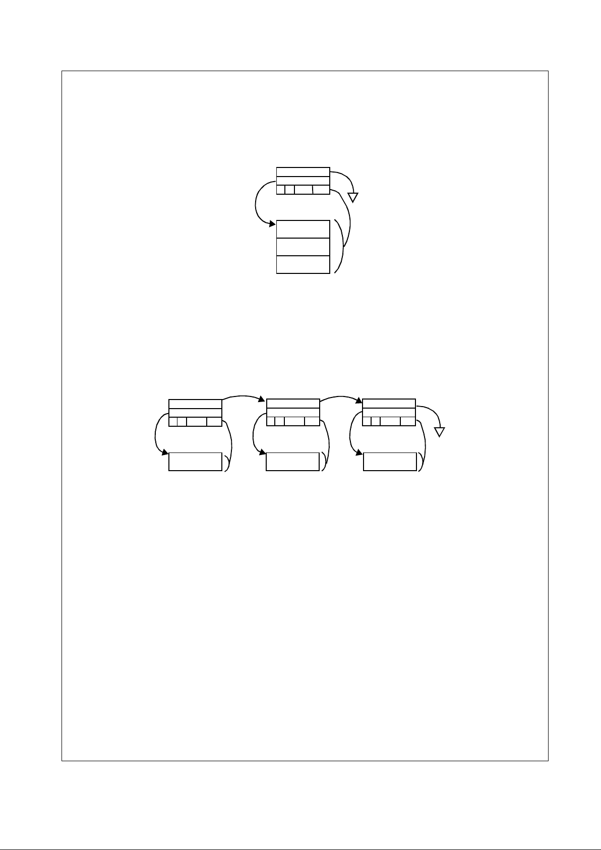
3.13 Buffer Management
The buffer management scheme used on the DP83820
allows quick, simple and efficient use of the frame buffer
memory. Frames are saved in similar formats for both
transmit and receive. The buffer management scheme also
uses separate buffers and descriptors for packet
information. This allows effective t ransfers of data from the
receive buffer to the transmit buffer by simply transferring
the descriptor from the receive queue to the transmit
queue.
The format of the descriptors allows the packets to be
saved in a number of configurations. A packet can be
stored in memory with a single descriptor and a single
packet fragment, or multiple descriptors with single
fragments. This flexibility allows the user to configure the
DP83820 to maximize efficiency. Architecture of the
specific system’s buffer memory, as well as the nature of
network traffic, will determine the most suitable
configuration of packet descriptors and fragments.
3.13.1 Overview
The buffer management design has the follow ing goals:
— simplicity
— efficient use of the PCI bus (the overhead of the buffer
management technique is minimal),
— low CPU utilization,
— flexibility.
Descriptors may be either per-packet or per-packetfragment. Each descriptor may describe one packet
fragment. Receive and transmit descriptors are
symmetrical.
3.13.2 Descript or Format
DP83820 uses a symmetrical format for transmit and
receive descr iptors. In br idging and switching applications
this sym m e try allows so f tware to forward packets by simp l y
moving the list of descriptors that describe a single
received packet from the receive list of one MAC to the
transmit list of another. Descriptors must be aligned on a
64-bit boundary.
TXPktsErrored RFC 1213 software, increment on
receive packets with
cmdsts.TXA set
This coun t er is in cr em ente d for each pack et
encountering errors during transmissi on.
This count does include t ransmissions
abor ted manuall y and due to FIFO
underruns, but does not include packets
which experience less than 16 in-window
collisions.
TXExcessiveCollisions RFC 1643,
802.3 LM
software, increment on
transmit packets with
cmdst s. EC se t .
This counter is incremented for each
transmission aborted af ter experiencing 16
in-window co ll is ions.
TXExcessiveDeferral 802.3 LM software, increment on
transmit packets with
cmdst s. ED se t .
This counter is incremented for each
transmission aborted due to a time-out of
the excessive deferral timer (3.2ms).
TXOWC RFC 1643,
802.3 LM
software, increment on
transmit packets with
cmdst s. OWC se t .
This counter is incremented for each
transmission which is aborted due to an
out-of-window collision.
TXCSErrors RFC 1643,
802.3 LM
software, increment on
transmit packets with
cmdst s. CR S se t .
This counter is incremented for each
transmission on which carrier is not
detected after the start of transmission, or
carrier sense is lost during tr ansmission.
TXSQEErrors RFC 1643 hardware, see
MIB:TxSQEErrors
This counter is incremented when the
collision heartbeat pulse is not detected
from by the PMD after a transmission.
Page 19

3.0 Functional Description
(Continued)
19
www.national.com
Table 3-2 DP83820 Descriptor Format
If 64-bit addressing is enabled, the link and bufptr fields are
64-bit fields. Otherwise, they are 32-bit fields. The
DP83820 supports an optional extended status field which
supports VLAN and IP functions. To enable the extsts field,
software should set the EXTSTS_EN bit in the CFG
register.
Some of the bit definitions in the
cmdsts
field are common
to both receive and transmit descriptors:
Table 3-3
cmdsts
Common Bit Definitions
Table 3-4 Tra nsmit
cmdsts
Bit De fin i tions
offset tag description
0000h link 32- or 64-bit "link" field to the next descriptor in the linked list. Bits 2-0 must be 0, as
descriptors must be aligned on 64-bit boundaries.
0004h or
0008h
bufptr 32- or 64-bit pointer to the first fragment or buffer. In transmit descriptors, the buffer can
begin on any byte boundary. In receive descriptors, the buffer must be aligned on a 64-bit
boundary.
0008h or
0010h
cmdsts 32-bit Command/Stat us Field (bit-encoded)
000ch or
0014h
extsts OPTIONAL 32-bit Extended Status Field. Contains VLAN and IP information.
bit tag description usage
31 OWN Descrip tor O w ne rsh i p Set to 1 by the data producer of the descriptor to transfer
owner s hi p to t h e da ta consumer of the descriptor. Set to 0 by
the data consumer of the descriptor to return ownership to
the data producer of the descriptor. For transmit descriptors,
the driver is the data producer, and the DP83820 is the data
consumer. For receive descriptors, the D P83820 is the data
producer, and the driver is the data consumer.
30 MORE More descriptors Set to 1 to indicate that this is NOT the last descriptor in a
packet (there are MORE to follow). When 0, this descriptor is
the last descriptor in a packet. Completion status bits are
only valid whe n t hi s bi t is zero.
29 INTR Interrupt Set to 1 by software to request a "descriptor interrupt" when
DP838 20 transfers the ownership of this descriptor back to
software.
28 SUPCRC
INCCRC
Suppress CRC / Include
CRC
In tr an smit d es cript o rs, t his indi ca t es th at CRC s ho uld no t be
appended by the MAC. On receives, this bit will be set based
on the RXCFG:INCCRC bit.
27 OK Packet OK In the last descriptor in a packet, this bit indicates that the
pac ket was either se nt or received successfully.
26-16 --- The usage of these bits differ in receive and transmit
descriptors. See below for details.
15-0 SIZE Descriptor Byte Count Set to the size in bytes of the data.
bit tag description usage
26 TXA Transmit Abort Transmission of this packet was aborted.
25 TFU Transmit FIFO Underrun The transmi t FIFO wa s e x ha uste d du ring the tr ans mi ssi on of
this packet.
24 CRS Carrier Sen s e Los t Carrier was lost during the transmission of this packet. This
condition is not reported if TXCFG:CSI is set.
23 TD Transmit Deferred Transmission of this packet was deferred.
22 ED Excessive D eferral The length of deferral during the transmission of this packet
was excessive.
21 OWC Out of Window Collision The MAC encountered an "out of window " collision during
the transmission of this packet.
Page 20

3.0 Functional Description
(Continued)
20
www.national.com
Table 3-5 Receive
cmdsts
Bit Definitions
20 EC Excessive Collisions The number of collisi ons during the transmission of this
packet was excessive, indicating transmission failure.
If TXCFG register ECRETRY=0, this bit is set after 16
collisions.
If TXCFG register ECRETRY=1, this bit is set after 4
Excessive Collision events (64 collisions).
19-16 CCNT Collision Count If TXCFG register ECRETRY=0, this field indicates the
numb er of collisions e ncountered during the transmission of
this packet.
If TXCFG register ECRETRY=1,
CCNT[3:2] = Excessive Collisions (0-3)
CCNT[1] = Multiple Collisions
CCNT[0] = Single Collision
Note that Excessive Collisions indicate 16 attempts failed,
while Multiple Col li si on s an d S in gle Co ll is io n ind ic ate
collisions in addition to any excessive collisions. For
example, a collision count of 33 includes 2 Excessive
Collisions and will also set the Single Collision bit.
bit tag description usage
26 RXA Receive Aborted Set to 1 by DP83820 when the receive was aborted. If RXO
is set, then the receive was aborted due to an RX overrun. If
RXO is clear, then a receive descriptor error occurred. SIZE
will be set to the amount of data that was transferred to
memory when the error was detected.
25 RXO Receive Overr un Set to 1 by DP83820 to indicate that a receive overrun
condi tion occurred. RXA will also be set.
24-23 DEST Destination Class When the receive filter is enabled, these bits will indicate the
destination address class as follows:
00 - Packet was rejected
01 - Destination matched the Receive Filter Node Address
Register
10 - Destination is a multicast (but not broadcast)
11 - Destination is a broadcast address
If the R eceive Filter is enabled, 00 indicates that the packet
was rejec ted . N ormally packets that are rejecte d do not
cause any bus activity, nor do they consume receive
descriptors. However, this condition could occur if the packet
is rejected by the Receive Filter later in the packet than the
receive drain threshold (RXCFG:DRTH)
22 LONG Too Long Packet
Received
The size of the receive packet exceeded 1518 bytes (1522
bytes if VLAN tag included ).
21 RUNT R u nt Packet Rec e ived The size of the receive packet was smaller than 64 bytes
(including CRC).
20 ISE Invalid Symbol Error (100 Mb only) An invalid symbol wa s enc ount er ed du ri ng the
reception of this packet.
19 CRCE CRC Error The CRC appended to the end of thi s packet was invalid.
18 FAE Frame Alignment Er ror Th e packet did not contain an integral number of octets.
17 LBP Loopback Packet The packet is the result of a loopback transmission.
16 IRL In-Ran ge Length Error The receive packet Length/Type field did not match the
length of the data field for the packet. Only valid if the
Length/Type field is a valid length (not a Type value).
Page 21

3.0 Functional Description
(Continued)
21
www.national.com
Table 3-6 Transmit
extsts
Bit De fin i tions
T able 3-7 Receive
extsts
Bit Defi n itions
bit tag description usage
31-22 unused
21 UDPPKT UDP Packet Indicates packet contains a UDP header and enables
checksum generation for the UDP header if Checksumming
is ena bled on a per-pa cket basis .
20 unused
19 TCPPKT TCP Packet Indicate s packet contains a TCP header an d enables
checksum generation for the TCP header if Checksumming
is ena bled on a per-pa cket basis .
18 unused
17 IPPKT IP Packet Indicates packet contains a IP header and enables
checksum generation for the IP header if Checksumming is
enabled on a per- pa cket basis.
16 VPKT VLAN Packet Inser t VLAN tag.
15-0 VTCI VLAN Tag Control
Information
This is the VLAN TCI field to be inserted in the packet if the
VPKT bit is set.
bit tag description usage
31-23 unused
22 UDPERR UDP Checksum Error Indicates a checksum error was detected in the UDP header.
21 UDPPKT UDP Packet Indicates an UDP header was detecte d for the packet.
20 TCPERR TCP Checksum Error Indicates a checksum error was detected in the TCP header.
19 TCPPKT TCP Packet Indicate s an TCP header was detected for the pack et.
18 IPERR IP Checksum Error Indicates a checksum error was detected in the IP header.
17 IPPKT IP Packet Indicates an IP header was detected for the packet.
16 VPKT VLAN Packet Packet contained a VLAN tag. This bit will be set if VLAN
packet detectio n is enabled and the packet contained the
correct ty pe value.
15-0 VTCI VLAN Tag Control
Information
This is the VLAN TCI field to be extracted from the packet. It
contain s the us er _ prior ity, CFI, and VID fi e lds .
Page 22
3.0 Functional Description
(Continued)
22
www.national.com
3.13.2.1 Single Descriptor Packets
To represent a packet in a single descript or, the MORE bit in the
cmdsts
field is set to 0.
Figure 3-10 Single Descripto r Packets
3.13.2.2 Mult ipl e Descriptor Packets
A single packet may also cross descriptor boundaries. This
is indicated by setting the MORE bit in all descriptors
except the last one in the packet. Ethernet inter-networking
applications (bridges, switches, router s, etc.) can optimize
memory utilization by using a single small buffer per
receive descr iptor, and allowing the DP83820 hardware to
use the minimum number of buffers necessary to store an
incoming packet.
Figure 3-11 Multiple Descriptor Packets
3.13.2.3 Descriptor Rings
The simplest and recommended organization of
descriptors is in a fixed ring implementation. At
initialization, the driver can set up a fixed list of descriptors
complete with links connecting the descriptors in a ring. All
descriptors will initially be owned by the producer of the
data (the driver for transmit, the DP83820 for receive). The
OWN bit is used by both driver and the DP83820 to
indicate data availability and to release descriptors back to
the producer. When using a descriptor ring, the driver
should never need to modify any fields of a descriptor it
does not own. For transmit, the driver should never assign
all descriptors to the device, reserving one descriptor to
terminate the list, preventing the device from wrapping
completely around the ring.
link
bufptr
MAC hdr
netwk hdr
data
0
64
single descriptor / single fragment
link
bufptr
MAC hdr
netwk hdr
data
1
14
multiple descriptor / single fragment
link
bufptr
1
20
link
bufptr
0
30
Page 23
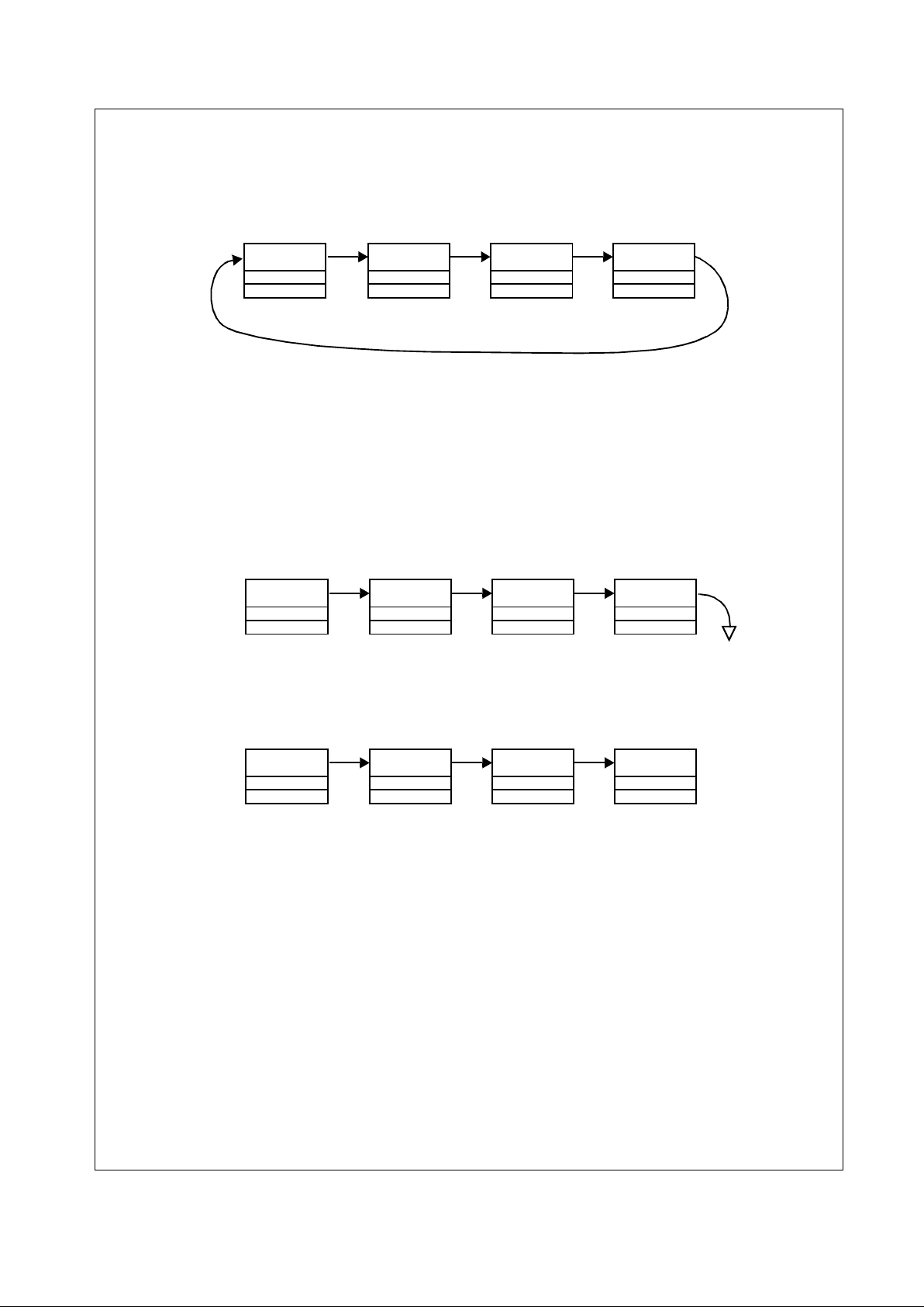
3.0 Functional Description
(Continued)
23
www.national.com
Figure 3-12 Ring Descriptor Organization
3.13.2.4 Descriptor Lists
Descriptors may also be organized in linked lists using the
link field. The linked list may be terminated by either a
NULL link field, or by using the descriptor OWN bit. A list of
descriptors ma y repres ent any num ber of pac k ets or pac ke t
fragments. Care should be used when implementing a
linked list terminated by a NULL link as there is a potential
for driver software and the device to get out of sync. Before
clearing a link field when freeing up descriptors, the driver
should verif y that the device has al ready traversed the li nk.
Figure 3-13 Linked List Descr iptor Organization
10180
addr 10140
10140
addr 10100
101C0
addr 10180
10100
addr 101C0
Descriptors Organized in a Ring (Recommended Method)
10180
addr 10140
10140
addr 10100
101C0
addr 10180
addr 101C0
Linked List terminated by OWN bit
10180
addr 10140
10140
addr 10100
101C0
addr 10180
00000
addr 101C0
Linked List terminated by NULL li nk field
own !own
ownown
Page 24
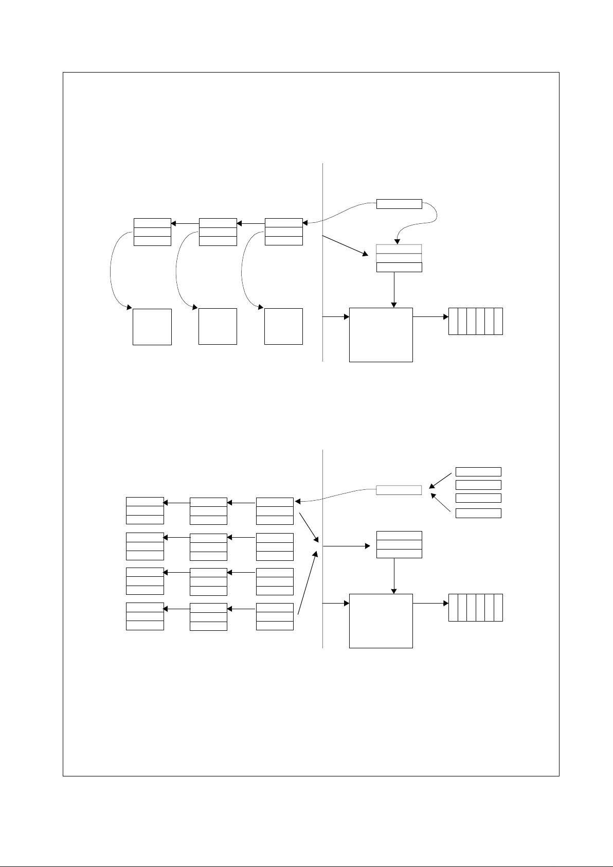
3.0 Functional Description
(Continued)
24
www.national.com
3.13.3 Transmit Architecture
The Transmit architecture can support a single transmit
queue, or can support multiple transmit queues for
handling priority traf fic. The following figures illustrate t he
transmit architecture of the DP83820 10/100 Ethernet
Controller with and without Priority Queueing.
Figure 3-14 Transmit Architecture without Priority Queueing
Without Priority Queueing, the device will draw packets
from a single Descriptor list. Only one descriptor pointer is
required. When the CR:TXEN bit is set to 1 (regardless of
the current state), and the DP83820 tr ansmitter is idle, t hen
DP83820 will read the contents of the current transmit
descriptor into the TxDescCache. The DP83820’s
TxDescCache can hold a single fragment pointer/count
combination.
Figure 3-15 Transmit Architecture with Prior ity Queueing
With Priority Queueing, the device will draw packets from
up to 4 Descriptor lists. The device has four descriptor
pointers and associated control logic to keep track of when
descriptors are available with valid packet information. In
this case, pulsing CR:TXEN with CR:TXPRI[p] set will
indicate to the DP83820 that a descriptor is available for
descriptor queue of priority ‘p’. Based on the priority
algorithm in use, the device will draw from the current
highest priority descriptor that has packets available for
transmission. There is no reordering of packets once they
are queued within the internal FIFO.
Transmit Descr iptor
Current Tx Desc Ptr
Software/Memory Hardware
Tx Data FIFO
link
bufptr
cmdsts
cmdsts
Tx DMA
bufptr
Packet
TxHead
link
Tx Desc Cache
link
bufptr
cmdsts
Packet
link
bufptr
cmdsts
Packet
Transmit Descr iptor
Current Tx Desc Ptr
Software/Memory Hardware
Tx Data FIFO
link
bufptr
cmdsts
cmdsts
Tx DMA
bufptr
TxHead
link
Tx Desc Cache
link
bufptr
cmdsts
link
bufptr
cmdsts
link
bufptr
cmdsts
link
bufptr
cmdsts
link
bufptr
cmdsts
link
bufptr
cmdsts
link
bufptr
cmdsts
link
bufptr
cmdsts
link
bufptr
cmdsts
link
bufptr
cmdsts
link
bufptr
cmdsts
TXDP1
TXDP2
TXDP3
TXDP4
Q0
Q1
Q2
Q3
Page 25

3.0 Functional Description
(Continued)
25
www.national.com
3.13.3.1 Trans mit Sta te Machine
The transm it state machine has the following states:
The transm it state machine manipulates the following i nternal data spaces:
Inputs to the transmit state machine include the following events:
T able 3-8 Transmit State Tables
txIdle The transmit state machine is idle.
txDescRefr Wait ing for the "r efresh" transfer of the link field of a completed descri ptor from the PCI bus.
txDescRead Waiting for the transfer of a complete descriptor from the PCI bus into the
TxDescriptorCache.
txFifoBlock Waiting for free space in the TxDataFIFO to reach TxFillThreshold.
txFragRead Waiting for the transfer of a fragment (or portion of a fragment) from the PCI bus to the
TxDataFIFO.
txDescWrite Waiting for the completion of the write of the
cmdsts
field of an intermediate transmit
descriptor (cmdsts.MORE == 1) to host memory .
txAdvance (transitory state) Examine the link field of the current descriptor and advance to the next
descriptor if link is not NULL .
TXDP A 32- or 64-bit register that points to the current transmit descriptor. If priority queueing is
enabled, this points to the available transmit descriptor with the highest priority.
CTDD Current Transmit Descriptor Done. An internal bit flag that is set when the current transmit
descriptor has been compl eted, and ownership has been returned to the driver. It is cleared
whenever TXDP is loaded with a new value (either by the state machine, or the driver).
TxDescCache An internal data space equal to the size of the maximum transmit descriptor supported.
descCnt Count of bytes remaining in the current descriptor.
fragPtr Pointer to the next unread byte in the current fragment.
txFifoCnt Current amount of data in the txDataFifo in bytes.
txFifoAvail Current amount of free space in the txDataFifo in bytes (size of the txDataFifo - txFifoCnt).
CR:TXEN Driver asserts the TXEN bit in the command register. If priority queueing is enabled, this
corresponds to a specific priority queue.
XferDone Completion of a PCI bus transfer request.
FifoAvail TxFifoAvail is gr e ater than TxFillThreshold.
state event next state actions
txIdle CR:TXEN && !CTDD txDescRead start a burst transfer at address TXDP and a
length derived from TXCFG.
CR:TXEN && CTDD txDescRefr start a burst transfer to refresh the link field of the
current descriptor.
txDescRefr XferDone txAdvance
txDescRead XferDone && OWN txFIFOblock
XferDone && !OWN txIdle set ISR:TXIDLE.
txFIFOblock FifoAvail txFragRead start a burst transfer into the TxDataFIFO from
fragP tr. The len gt h wi ll be the minimum of
txFifoAvail and des c C nt .
Decrement desc C nt accordingly.
(descCnt == 0) && MO RE txDescWrite start a burst tr an sf er to w rite the st at u s bac k t o th e
descriptor, clearing the OWN bit.
(descCnt == 0) && !MORE txAdvance write the value of TXDP to the txDataFIFO as a
handle.
txFragRead XferDone txFIFOblock
txDescWrite XferDone txAdvance
Page 26
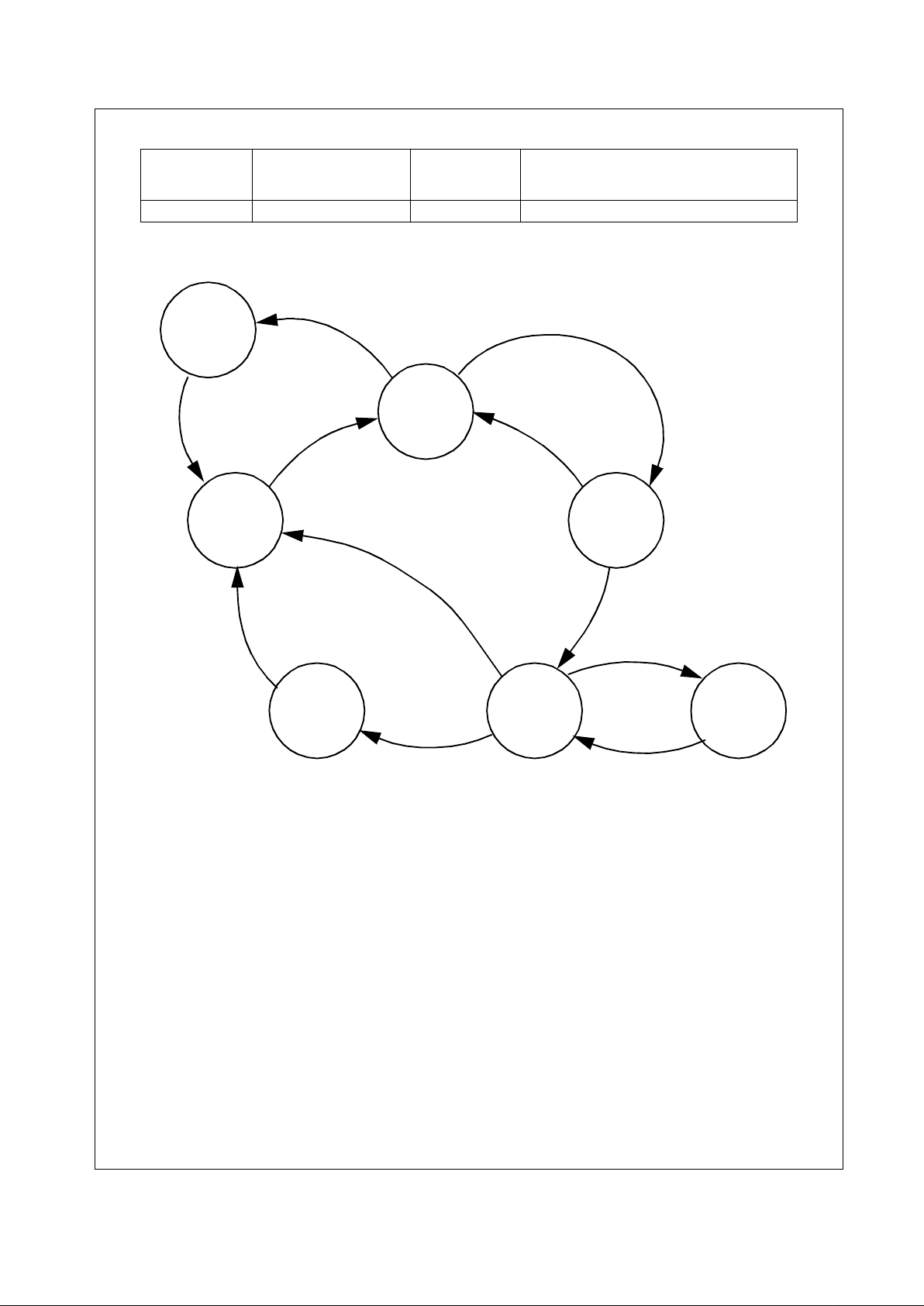
3.0 Functional Description
(Continued)
26
www.national.com
Figure 3-16 Transmit State Di agram
3.13.3.2 Transmit Data Flow without Priority Queueing
In the DP83820 transmit architecture without Priority
Queueing, packet transmission involves the following
steps:
1. The device driver receives packets from an upper
layer.
2. An available DP83820 transmit descriptor is
allocated. The fragment information is copied from
the NOS specific data structure(s) to the next
DP83820 transmit descriptor .
3. The driver adds this descriptor to it’s internal li st of
transmit descr ipt ors awaiting transmission.
4. If the internal list was empty (this descriptor
represents the only outstanding transmit packet),
then the driver must set the TXDP register to the
address of this descriptor, else the driver will append
this descriptor to the end of the list.
5. The driver sets the TXEN bit in the CR register to
insure that the transmit state machine is active.
6. If idle, the transmit st ate machine reads the des criptor
into the TxDescript orCache. If the OWN bit is not set ,
the trans mi t sta te ma chi ne re turn s to id le to wait for
TXEN to be set again.
7. The state machine then moves through the fragment
described wi thin the descriptor, filling the TxDataFifo
with data. The hardware handles all aspects of byte
alignment; no alignment is assumed. Fragments
may start and/or end on any byte address. The
transmit state machine uses the fragment pointer
and the SIZE field from the
cmdsts
field of the
current descr iptor to keep the TxDataFifo full. It also
uses the MORE bit and the SIZE field from the
cmdsts
field of the current descriptor to know when
packet boundaries occur.
8. When a packet has completed transmission
(successful or unsuccessful), the state machine
updates the
cmdsts
field of the current descriptor in
main memory (by bus-mastering a single 32-bit
word), relinquishing ownership, and indicating the
packet complet ion stat us. If mor e than one des criptor
txAdvance link != NULL txDescRead TXDP <- txDescCache.link. Clear CTDD. Start a
burst transfer at address TXDP with a length
derived from TXCFG.
link == NULL txIdle set CTDD. set ISR:TXIDLE.
txDescRefr
txIdle
txDescRead
txFifoBlocktxDescWrite
txAdvance
txFragRead
CR:TXEN && CTDD
CR:TXEN && !CTDD
XferDone
XferDone
XferDone
XferDone && OWN
XferDone && !OWN
|| link != NULL
descCnt == 0 && !(cmdsts & MORE)
descCnt == 0 && (cmdsts & MORE)
FifoAvail
Page 27
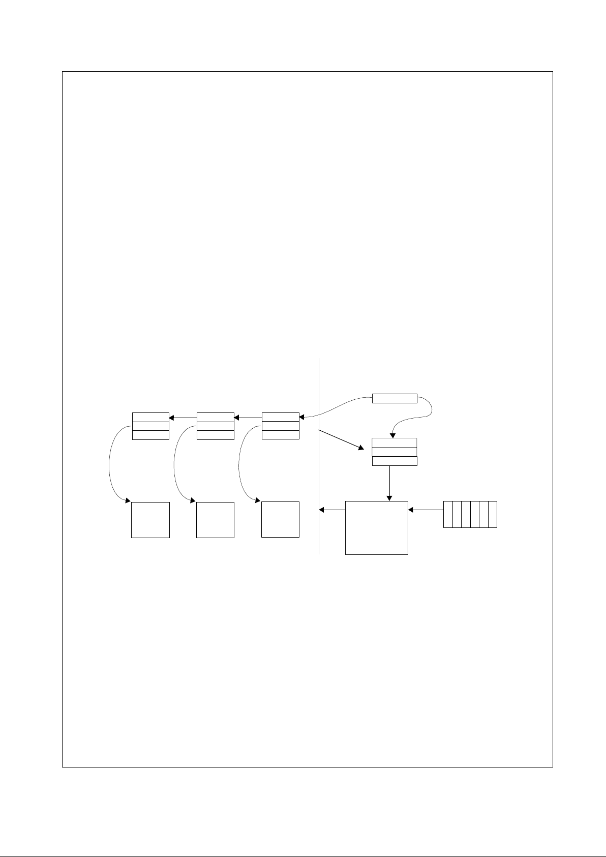
3.0 Functional Description
(Continued)
27
www.national.com
was used to describe the packet, then completion
status is updated only in the last descriptor.
Intermediate descriptors only have the OWN bits
modified.
9. If the link field of the descriptor is non-zero, the state
machine advances to the next descriptor and
continues. When reading the next descriptor, if the
OWN b it is not s et, the s tate mach ine will halt and
wait for TXEN to be set again.
10. If the link field is NULL, the transm it state machine
suspends, wait ing for t he TXEN b it in t he CR r egiste r
to be set. If the TXDP r egiste r is written t o, t he CTDD
flag will be cleared. When the TXEN bit is set, the
state machine will examine CTDD. If CTDD is set,
the state machine will "refresh" the link field of the
current descriptor. It will then follow the link field to
any new descriptor s that have bee n added to the end
of the list. If CTDD is clear (implying that TXDP has
been written to), the state machine will start by
reading in the descri ptor pointed to by TXDP.
3.13.3 .3 T ransmit Data Flow with Priority Queueing
The transmit architecture with Priority Queueing is the
same with a few min or di fferences:
— Driver keeps a separate list for each descriptor queue.
— When setting the TXEN bit, the driver must also set the
appropriate TXPRI bit for the prior ity queu e or queues to
which descriptors are being appended.
— Upon completion of a packet , the t ransm it state mach ine
first determines what the highest priority descriptor is
available based on non-zero link fields and TXEN bits. It
then follows the appropriate link or reads a new
descriptor for the next packet to be transmitted.
3.13.4 Receive Architecture
The receive architecture is as "symmetrical" to the transmit
architecture as possible. As is done in the transmitter, the
receive architecture can support a single descriptor queue
or multiple descriptor queues for handling priority traffic.
When the amount of receive data in the RxDataFIFO is
more than the RxDrainThreshold, or the RxDataFIFO
contains a complete packet, then the state machine begins
filling received buffers in host memo ry.
Figure 3-17 Receive Architecture without Priority Queuei ng
Without Priority Queueing, the device will transfer packets
to a single Descriptor list. Only one descriptor pointer is
required. The receive buffer manager prefetches receive
descriptors to prepare for incoming packets. When the
RXEN bit is set to 1 in the CR register (regardless of the
current state), and the DP83820 recei ve stat e machine is
idle, then DP83820 will read the contents of the descriptor
referenced by RXDP into the Rx Descriptor Cache. The Rx
Descriptor Cache allows the DP83820 to read an entire
descriptor in a single burst, and reduces the number of bus
accesses required for fragment information to 1. The
DP83820 Rx Descriptor Cache holds a single buffer
pointer/count combination.
Recieve Descriptor List
Current Rx Desc Ptr
Software/Memory Hardware
Rx Data FIFO
link
bufptr
cmdsts
cmdsts
Rx DMA
bufptr
Packet
RxHead
link
Rx Desc Cache
link
bufptr
cmdsts
Packet
link
bufptr
cmdsts
Packet
Page 28

3.0 Functional Description
(Continued)
28
www.national.com
Figure 3-18 Receive Archite cture with Priority Queueing
With Priority Queueing, the device will transfer packets
onto up to 4 Descript or l ists. The device has four descriptor
pointers and associated control logic to keep track of when
descriptors are available with valid packet information. The
Receiver uses the user_priority field of a VLAN tag to
determine the priority, based on the 802.1Q encodings
based on the number of priority queues enabled. If the
packet has no VLAN tag, then a priority of 0 is assumed.
There is no reorderi ng of packets while in the Receive Data
FIFO.
3.13.5 Receive State Machine
The receive st ate machine has the following states:
The receive state machine manipulates the following internal data spaces:
Inputs to the receive state machine include the following events:
Receive Descriptor List
Current Rx Desc Ptr
Software/Memory Hardware
Rx Data FIFO
link
bufptr
cmdsts
cmdsts
Rx DMA
bufptr
RxHead
link
Rx Desc Cache
link
bufptr
cmdsts
link
bufptr
cmdsts
link
bufptr
cmdsts
link
bufptr
cmdsts
link
bufptr
cmdsts
link
bufptr
cmdsts
link
bufptr
cmdsts
link
bufptr
cmdsts
link
bufptr
cmdsts
link
bufptr
cmdsts
link
bufptr
cmdsts
RXDP1
RXDP2
RXDP3
RXDP4
Q0
Q1
Q2
Q3
rxIdle The receive state machine is idle.
rxDescRefr Waiting for the "refresh" transfer of the link field of a completed descriptor from the PCI bus.
rxDescRead Waiting for the transfer of a descriptor from the PCI bus into the RxDescCache.
rxFifoBlock Waiting for the amount of data in the RxDataFifo to reach the RxDrainThreshold or to
represe nt a complete packet.
rxFragWrite Waiting for the transfer of data from the RxDataFIFO via the PCI bus to host memory.
rxDescWrite Waiting for the completion of the write of the
cmdsts
field of a receive descriptor.
RXDP A 32- or 64-bit register that points to the current receive descriptor.
CRDD An internal bit flag that is set when the current receive descriptor has been completed, and
ownership has been returned to the driver. It is cleared whenever RXDP is loaded with a new
value (either by the state machine, or the driver).
RxDescCache An internal dat a space equal to the s ize of the maximum receive descriptor supported.
descCnt Count of bytes available for storing receive data in all of the fragments described by the current
descriptor.
fragPtr Pointer to the next unwritten byte in the current fragment.
rxPktCnt Number of packets in the rxDataFifo. Incremented by the MAC (the fill side of the FIFO).
Decremented by the receive state machine as packets are processed.
rxPktBytes Number of bytes in the cu rrent packet being drained from the r xDataFifo, that are in fact
currently in the rxDataFifo (Note: for packets larger than the FIFO size, this number will never
be greater than the FIFO size).
CR:RXEN The RXEN bit in the Command Register has been set.
XferDone completion of a PCI bus transfer request.
Page 29

3.0 Functional Description
(Continued)
29
www.national.com
Table 3-9 Receive State Tables
FifoReady (rxPktCnt > 0) or (rxPktBytes > rxDrainThreshold) ... in other words, if we have a complete
packet in the FIFO (regardless of size), or the number of bytes that we do have is greater than
the rxDrainThreshold, then we are ready to begin draining the rxDataFifo.
state event next state actions
rxIdle CR:RXEN && !CRDD rxDescRead start a burst transfer at addr ess RXDP and a
length derived from RXCFG.
CR:RXEN && CRDD rxDescRefr start a burst transfer to refresh the link field of the
current descriptor.
rxDescRefr XferDone rxAdvance
rxDescRead XferDone && !OWN rxFIFOblock
XferDone && OWN rxIdle set ISR:RXIDLE.
rxFIFOblock FifoReady rxFragWrite start a burs t tran sfer from th e RxDat aFIF O to host
memory at fragPtr. The length will be the
minimu m of rxPktBytes and descCnt. Decrement
descCnt accordingly.
(desc Cnt == 0) &&
(rxPktBytes > 0)
rxDescWrite start a burst transfer to write the status back to
the descriptor, setting the OWN bit, and setting
the MORE bit. We'll continue the packet in the
next desc riptor.
rxPktBytes == 0 rxDescWrite start a transfer to write the cmdsts back to the
descriptor, setting the OWN bit and clearing the
MORE bit, and filling in th e final receiv e status
(CRC, FAE, SIZE, etc.).
rxFragWrite XferDone rxFIFOblock
rxDescWrite XferDone rxAdvance
rxAdvance link != NULL rxDescRead RXDP <- rxDescCache.link. Clear CRDD. Start a
burst transfer at address RXDP with a length
deri ved fr om RX CF G: M AXF.
link == NULL rxIdle set CRDD. S et ISR:RXIDLE.
Page 30

3.0 Functional Description
(Continued)
30
www.national.com
Figu re 3- 1 9 R eceive Stat e D i a g ram
3.13.5.1 Receive Da ta Fl ow without Priority Queueing
With a bus mastering architecture, some number of buffers
and descriptors for received packets must be pre-allocated
when the DP83820 is initialized. The number allocated will
directly affect the system's tolerance to interrupt latency.
The more buffers that you pre-allocate, the longer the
system will survive an incoming burst wi thout losing receive
packets, if receive descriptor processing is delayed or
preempted. The following describes the Receive data flow
without Priority Queueing:
1. Prior to packet reception, receive buffers must be
described in a receive descriptor ring (or list, if
preferred). In each descriptor, the driver assigns
ownership to the hardware by clearing the OWN bit.
Receive descriptors m ay describe a single buffer.
2. The address of the first descriptor in this list is then
written to the RXDP register. As packets arr ive, they
are placed in available buffers. A single packet may
occupy one or more receive descriptors, as required
by the application.The device reads in the first
descriptor into the RxDescCache.
3. As data arrives in the RxDat aFIF O, the r eceive b uffer
management state machine places the data in the
receive buffer described by the descriptor. This
continues un til eith er the end of pac ket is r eached, or
the descriptor byte count for this descriptor is
reached.
4. If end of packet was reached, the status in the
descriptor (in main memor y) is updat ed by sett ing the
OWN bit and clearing the MORE bit, by updating the
receive status bits as indicated by the MAC, and by
updating the SIZE field. The status bits in
cmdsts
are only v alid in the la st des crip tor of a pac ket (with
the MORE bit clear). Also for the last descriptor of a
packet, the SIZE field will be updated to reflect the
actual amount of data written to the buffer (which
may be less the full buffer size allocated by the
descriptor).
If the receive buffer management state machine runs out of
descriptors while receiving a packet, data will buffer in the
receive FIFO. If the FIFO overflows, the driver will be
interrupted with an RxOVR error.
rxDescRefr
rxIdle
rxDescRead
rxFifoBlockrxDescWrite
rxAdvance
rxFragWrite
CR:RXEN && CRDD
CR:RXEN && !CRDD
link = NULL
XferDone
XferDone
XferDone
XferDone && !OWN
XferDone && OWN
link != NULL
(descCnt == 0) && (rxPktBytes > 0)
FifoReady
rxPktBytes == 0
Page 31

3.0 Functional Description
(Continued)
31
www.national.com
3.13.5.2 Receive Da ta Fl ow with Pri ority Queueing
With Priority Queueing, it is still necessary to pre-allocate
buffers and descriptors. Each priority queue must have a
separate list of descriptors allocat ed. The receive data flow
is similar to the above with the following exceptions:
— The Receive state machine waits until packet data is
available, and the priority for the packet has been
determined f rom a VLAN tag (assu mes p rior ity 0 if no tag
is present). Using this information, the receive state
machine will then process desc riptors as detailed above .
— If no descriptors are available for the priority queue
matching the packet priority, the state machine will wait
for the system to append more descriptors to the
descriptor list and pulse the CR:RXEN and CR:RXPRI
controls.
— If no descriptors are available for the priority queue
matching the packet priority, the state machine will wait
for the system to append more descriptors to the
descriptor list and pulse the CR:RXEN and CR:RXPRI
controls.
Page 32

32
www.national.com
4.0 Register Set
4.1 Configuration Registers
The DP83820 implements a PCI version 2.2 configurat ion register space. This allows a PCI BIOS to "soft " configure the
DP83820. Software Reset has no effect on configuration registers. Hardware Reset returns all configuration registers to
their hardware reset state. For all unused registers, writes are ignored, and reads return 0.
Table 4-1 Configuration Register Map
4.1.1 Configurati on Identification Register
This register i dentifies the DP83820 Cont rol ler to PCI system softw are.
offset tag description access
00h CFGID Configuration Identification Register RO
04h CFGCS Configuration Command and Status Register R/W
08h CFGRID Configuration Revision ID Register RO
0Ch CFGLAT Configuration Latency Timer Register RO
10h CFGIOA Configuration IO Base Address Register R/W
14h CFGMA Configuration Memory Address Register R/W
18 CFGMA1 Configuration Memory Address High Dword Register R/W
1Ch-28h Reserved (reads return zero)
2Ch CFGS ID Configuration Subsystem Iden tification Register RO
30h CFGROM Boot ROM configuration register R/W
34h CAPPTR Capabilit ies Pointe r Register RO
38h Reserved (reads return zero)
3Ch CFGINT Configuration Interrupt Select Register R/W
40h PMCAP Power Management Capabilities Register RO
44h PMCS Power Management Control and Status Register R/W
48-FFh Reserved (reads return zero)
Tag: CFGID Size: 32 bits Hard Reset: 0022100B
Offset: 00h Access: Read Only Soft Reset: Unchanged
bit tag description usage
31-16 DEVID Device ID This field is read-only and is set to the device ID assigned by NSC to the
DP83820, which is 0022h.
15-0 VENID Vendor ID This field is read-only and is set to a value of 100Bh w hich is National
Semiconductor's PCI Vendor ID.
Page 33

33
www.national.com
4.0 Register Set
(Continued)
4.1.2 Configuration Command and Status Register
The CFGCS register has two parts. The upper 16-bits (31-16) are devoted to device status. The lower 16-bits (15-0) are
dev oted to command and are used to configure and control the device.
Tag: CFGCS Size: 32 bits Hard Reset: 02900000h
Offset: 04h Access: Read Write Soft Reset: Unchanged
bit tag description usage
31-16 STS Status Devic e S tat us Bi ts . A s tatu s b it i s r es et whe ne v e r the r e gi ster i s wri tte n, and
the corr e sp on ding bit loc a tio n is a 1.
31 DPERR Detected Parity Error Refer to the description in the PCI V2.2 specification.
30 SSERR Signaled SERR Refer to the description in the PCI V2.2 specification.
29 RMABT Received Master Abort Refer to the description in the PCI V2.2 specification.
28 RTABT Received Target Abort Refer to the description in the PCI V2.2 specification.
27 STABT Sent Target Abort Refer to the description in the PCI V2.2 specification.
26-25 DSTIM DEVSELN Timing This field will always be set to 01 indicating that DP83820 supports
“medium” DEVSELN timing.
24 DPD Data Parity Detected Refer to the description in the PCI V2.2 specification.
23 FBB Fast Back-to-Back Capable DP83820 will set this bit to 1.
22 unuse d (reads return 0)
21 M66_CAP 66M H z C ap able This field indicates the device is 66MHz capable. It will be loaded from
EEPROM.
20 NCPEN New Capabilities Enable When set , this bit indicates that the Capabilities Pointer cont ains a valid
value and new capabilities such as power management are supported.
When clear, new capabilities (CAPPTR, PMCAP, PMCS) are disabled. The
value in this register will either be loaded from the EEPROM or, if the
EEPROM is disabled, from a strap option at reset.
19-16 Unused Unused (reads return 0)
15-0 CMD Command Device Command bits (see below).
15-10 Unused Unused (reads return 0)
9 FBBEN Fast Back-to-Back Enable Set to 1 by the PCI BIOS to enable the DP83820 to do Fast Back-to-Back
transfers (FBB transfers as a master is not implemented in the current
revision).
8 S ERREN SERRN Enable When set, DP83820 will generate SERRN when an address parity error is
detected.
7 Unused Unused (reads return 0)
6 PERRSP Parity Error Response When set, DP83820 will assert PERRN on the detection of a data parity
error when acting as the target, and will sample PERRN when acting as the
initiator. When reset, data parity errors are ignored. The action taken is
specified by CFG: PESEL.
5 Unused Unused (reads return 0)
4 MWIEN Memory Write an d Invalidate
Enable
When set, DP83820 may use the Memory W rite and I nvalidate command
for qualifying transfers. If 0, Memory Write will always be used instead of
MWI. The DP83820 further qualifies enabling the MWI command using the
MWI_DIS bit in the CFG operational register.
3 Unused Unused (reads return 0)
2 BMEN Bus Master Enable When set, DP83820 is allowed to act as a PCI bus master. When reset,
DP83820 is prohibited from acting as a PCI bus master.
1 MSEN Memory Space Access When set, DP83820 responds to memory space accesses. When reset,
DP83820 ignores memory space accesses.
0 IOSEN IO Space Access When set, DP83820 responds to IO space accesses. When reset,
DP83820 ignores IO space accesses.
Page 34

34
www.national.com
4.0 Register Set
(Continued)
4.1.3 Configurati on Revision ID Register
This register stores the silicon revision number, revision number of software interface specification and lets the
configura ti on software know that it is an Ethernet controller in the class of netwo rk cont rol lers.
4.1.4 Configurati on Latency Timer Register
This register gives status and controls such miscellaneous functions as BIST, Latency timer and Cache line size.
DP83820 Bus Master Operations:
Based on cache line si ze, the DP83820 will use the following PCI commands for bus mastered tr ansfers:
0110 - Mem Read Single dword read transfers
1110 - Mem Read Line Read More than 1 dword but not acr oss a cacheline boundary
1100 - Mem Read Multiple Read transfers that cross a cacheline boundary
0111 - Mem Write Writes that do not exactly overwrite 1 or more cachelines
1111 - Mem Write Invalidate W ri tes that exactly overwrite 1 or more cachelines
Tag: CFGRID Size: 32 bits Hard Reset: 02000000h
Offset: 08h Access: Read Only Soft Reset: Unchanged
bit tag description usage
31-24 BASECL Base Class Returns 02h wh ich specifies a network controller.
23-16 SUBCL Sub Class Returns 00h which specifies an Ethernet contr oller.
15-8 P ROGIF Programming IF Retu rns 00h which specifies the first release of the DP8382 0.
7-0 REVID Silicon Revision Returns 00h which specifies the silicon revision.
Tag: CFGLAT Size: 32 bits Hard Reset: 00000000h
Offset: 0Ch Access: Read Write Soft Reset: Unchanged
bit tag description usage
31 BISTCAP BIST Capable Reads will always return 0.
30 BISTEN BIST Enable Reads will return a 0, writes are ignored.
29-16 Reserved Reads will return a 0, writes are ignored.
15-8 LAT La te ncy Time r Set by soft ware to the number of PCI clocks that DP83820 may hold the
PCI bus.
7-0 CLS Cache Line Size Set to the value of the system cache line size in dwords. Acceptable values
are pow ers of 2 less than or equal to 128. All other values will be
recognized as 0.
Page 35

35
www.national.com
4.0 Register Set
(Continued)
4.1.5 Configurati on IO Base Address Register
This register specifies the Base I/O address which is required to build an address map during configuration. It also
specifies the number of bytes required as well as an indication that it can be mapped into I/O space.
4.1.6 Configurati on Me mory Address Register
This register specifies the Base Memory address which is required to build an address map during configuration. It also
specifies the number of bytes required as well as an indication that it can be mapped into memory space.
4.1.7 Configurati on Memory Address High Dword Register
This register specifies the upper 32-bits of the Base Memory address which is required to build an address map during
configuration.
Tag: CFGIOA Size: 32 bits Hard Reset: 00000001h
Offset: 10h Access: Read Write Soft Reset: Unchanged
bit tag description usage
31-8 IOBASE Base IO Address This is set by software to the base IO address for the Operational Register
Map.
7-2 IOSIZE Size indication Read bac k as 0. This allows the PCI bridge to determine that th e DP83820
requires 256 bytes of I O spa c e.
1 Unused Unused (reads return 0).
0 IOIND IO Space Indicator Read Only. Set to 1 by DP83820 to indicate that DP83820 is capable of
being ma pped into IO space.
Tag: CFGMA Size: 32 bits Hard Reset: 00000000h
Offset: 14h Access: Read Write Soft Reset: unchanged
bit tag description usage
31-12 MEMBASE Memory Base Address This is set by software to the base address for the Operational Register
Map.
11-4 MEMSIZE Memory Size These bits return 0, which indicates that the DP83820 requires 4096 bytes
of Memory Space (the minimum recommended allocation).
3 MEMPF Prefetchable Read Only . Set to 0 by DP83820.
2-1 MEMLOC Location Selection Read Only. Set to 10 by DP83820 if target 64-bit addressing is enabled. Set
to 00 if 64-bit addressing is not enabled. 64-bit addressing capability is
loaded from EEPROM at power-up and is reflected in the CFG:T64ADDR
bit in operational register space.
0 MEMIND Memory Space Indicator Read Only. Set to 0 by DP8382 0 to in di cate that DP 83 82 0 is cap able of
being mapped into memory space.
Tag: CFGMA1 Size: 32 bits Hard Reset: 00000000h
Offset: 18h Access: Read Write Soft Reset: unchanged
bit tag description usage
31-0 MEMBASE1 Memory Base High Address This is set by software to the upper 32-bits of the base address for the
Oper ati ona l Regi ster Ma p. If 64-bit addr e ssi ng is dis abled then thi s fie ld wil l
be read-only and always return 0.
Page 36

36
www.national.com
4.0 Register Set
(Continued)
4.1.8 Configurati on Subsystem Identification Register
The CFGSID allows system software to distinguish between different subsystems based on the same PCI silicon. The
values in this register can be loaded from the EEPROM if configuration is enabled.
4.1.9 Boot ROM Configuration Register
4.1.10 Capabilities Pointer Register
This register stores the capabilities linked l ist offset into the PCI configuration space.
Tag: CFGSID Size: 32 bits Hard Reset: ?
Offset: 2Ch Access: Read Only Soft Reset: unchanged
bit tag description usage
31-16 SDEVID Subsystem Device ID Loaded fro m the EEPROM
15-0 SVENID Subsystem Vendor ID Loaded from the EEPRO M
Tag: CFGROM Size: 32 bits Hard Reset: 00000000h
Offset: 30h Access: Read Write Soft Reset: unchanged
bit tag description usage
31-16 ROMBASE ROM Base Address Set to the base address for the b oot ROM.
15-11 ROMSIZE ROM Size Read only. Set to 0 indicating a requirement for 64K bytes of Boot ROM
space
10-1 Unused unused (reads return 0)
0 ROMEN ROM Enable This is used by the PCI BIOS to enable accesses to boot ROM. This allows
the DP83820 to share the address decode logic between the boot ROM
and itself. The BIOS will copy the contents of the boot ROM to system RAM
before executing it. Set to 1 enables the address decode for boot ROM
disab ling access to operational target registers.
Tag: CAPPTR Size: 32 bits Hard Reset: 00000040h
Offset: 34h Access: Read Only Soft Reset: unchanged
bit tag description usage
31-8 unu s ed (reads return 0)
7-0 CLOFS Capabilities List Offset Offset into P CI confi guration space for the location of the first item in the
Capabilities Linked List, set to 40h to point to the PMCAP register.
Page 37

37
www.national.com
4.0 Register Set
(Continued)
4.1.11 Configurati on Interrupt Select Register
This register stores the interrupt line number as identified by the POST software that is connected to the interrupt
controller as well as DP83820 desired settings for maximum latency and minimum grant. Max latency and Min. latency
can be loaded from the EEPROM
4.1.12 Power Management Capabilities Regist er
This register provides information on the capabilities of the functions related to power management. This register also
contains a pointer to the next item in the capabiliti es list and the capabilit y ID for Po wer Management. This reg ister is only
visibl e if CFGCS[ 4] is set.
Tag: CFGINT Size: 32 bits Hard Reset: 340b0100h
Offset: 3Ch Access: Read Write Soft Reset: unchanged
bit tag description usage
31-24 MXLAT Maximum Latency The DP83820 desired setting f or Max Latency. The DP83 820 will initialize
this field to 52d ( 13 usec). The value in this register can be loaded from the
EEPROM.
23-16 MNGNT Minimum Grant The DP83820 d esired setting for Minimum Gr ant. The DP83820 will
initialize this field to 11d (2.75 usec). The value in this register can be
loaded from the EEPROM.
15-8 IPIN Interru pt Pin Read Only, always return 0000 0001 (INTA)
7-0 ILINE Interru pt Line Set to which line on the i nterrupt controller that the DP83820's interrupt pin
is connected to.
Tag: PMCAP Size: 32 bits Hard Reset: FF820001
Offset: 40h Access: Read Only Soft Reset: unchanged
bit tag description usage
31-27 PMES PME Support This 5 bit field indicates the power states in which DP83820 may assert
PMEN. A 1 indicates PMEN is enabled for that state, a 0 indicates PMEN is
inhibited in that state.
XXXX1 - PMEN can be asserted from state D0
XXX1X - PMEN can be asserted from state D1
XX1XX - PMEN can be asserted from state D2
X1XXX - PMEN can be asserted from state D3hot
1XXXX - PMEN can be asserted from state D3cold
The DP83820 will only report PME support for D3cold if auxiliary power is
detec ted on the 3VAUX pin, in addition thi s value can be loaded from the
EEPROM when in the D3cold state.
26 D2S D2 Support This bit is set to a 1 when the DP83820 supports the D2 state.
25 D1S D1 Support This bit is set to a 1 when the DP83820 supports the D1 state.
24-22 AUX_CURRENT 3 bit field for aux curr ent
requirement.
Aux_Current
- This 3 bit field reports the 3.3Vaux auxiliary current
requirements for the PCI function.
If PMEN generation from D3cold is not su pported by the
function(PMCAP[31]), this field returns a value of “000b” when read.
Bit 3.3Vaux
8 7 6
Max. Current Required
1 1 0 320 m A
0 0 0 0 (self powered)
21 DSI Device Specific Initialization This bit is set to 1 to indicate to the system that initialization of the DP83820
device is required (beyond the standar d PCI configuration header) before
the generic class device driver is able to use it. A 1 indicates that DP83820
requires a DSI sequence foll owing transition to the D0 uninitialized st ate.
This bit can be loaded from the EEPROM.
Page 38

38
www.national.com
4.0 Register Set
(Continued)
4.1.13 Power Management Control and Status Register
This register contains PM control and st atus information.
20 Reserved Reserved (reads return 0)
19 PMEC PME Clock Returns 0 to indicate PCI clock not needed for PMEN.
18-16 PMV Power Management Version This bit field indicates compliance to a specific PM specification rev level.
Currently set to 010b.
15-8 NLIPTR Next List Item Pointer Offset into PCI configuration space for the location of the next item in the
Capabilities Linked List. Returns 00 h as no other capabilities are offered.
7-0 CAPID Capability ID Always ret urns 01h for Power Management ID.
Tag: PMCSR Size: 32 bits Hard Reset: 00000000h
Offset: 44h Access: Read Write Soft Reset: unchanged
bit tag description usage
31-24 reserved (reads return 0)
23-16 BSE Bridge Support Extensions unus ed (reads return 0)
15 PMESTS PME Status Sticky bit which represents the state of the PME logi c, regardless of the
state of the PMEEN bit.
14-9 DSCALE Data Scale reserved (reads return 0)
8 PMEEN PME Enable When set to 1, this bit enables the assertion of the PME function on the
PMEN pin. When 0, the PMEN pin is forced to be inactive. This value can
be loaded from the EEPROM.
7-2 Reserved unused (reads return 0)
1-0 PSTATE Pow er St ate This 2 bit field is used both to determine the current power state of
DP83820, and to set a new power state.
00 - D0
01 - D1
10 - D2
11 - D3hot
Page 39

39
www.national.com
4.0 Register Set
(Continued)
4.2 Operational Regi sters
The DP83820 provides the following set of operational registers mapped i nto PCI memory space or I/O space. Writes to
reserved register locations are ignored. Reads to reser ved register locations return undefined values. When mapped to
I/O space, a 256 byt e window allows access to all the Operational Registers ( 00-FCh). When mapped into PCI memory
space, a 4096 byte w indow is enabled. In addition t o access to Operational Registers, the PCI Configuration Registers
can be read at addresses 200-2FCh. Other addresses provide aliased access to Operational Registers or read-only PCI
Configuration Registers.
Table 4-2 Operational Register Map
offset tag description access
00h CR Command Register R/W
04h CFG Configuration Regi ster R/W
08h MEAR EEPROM Access Register R/W
0Ch PTSCR PCI Test Control Register R/W
10h ISR Interrupt Stat us Register RO
14h IMR Interrupt Mask Register R/W
18h IER Interrupt Enable Register R/W
1Ch IHR Interrupt Holdoff Register R/W
20h TXDP Transmit Descriptor Pointer Register R/W
24h TXDP_HI Transmit Descri ptor Pointer High Dword Register R/W
28h TXCFG Transmit Conf iguration Register R/W
2Ch GPIOR General Purpose I/O Control Register R/W
30h RXDP Receive Descriptor Pointer Register R/W
34h RXDP_HI Receive Descriptor Poi nte r High Dword Regi ste r R/W
38h RXCFG Receive Configuration Registe r R/W
3Ch PQCR Priority Queueing Control Register R/W
40h WCSR Wake on LAN Control/Status Register R/W
44h PCR Pause Control/Status Regist er R/W
48h RFCR Recei ve Filter/Match Control Register R/W
4Ch RFDR Receive Fi lt er/ M atch Data Register R/W
50h BRAR Boot ROM Address R/W
54h BRDR Boot ROM Data R/W
58h SRR Silicon Revision Register RO
5Ch MIBC Management Informat ion Base Control Register R/W
60-88h MIB Management Information Base Data Registers RO
8C-9Ch Reserved
A0h TXDP1 Transmit Descriptor Pointer Priority 1 Register R/W
A4h TXDP2 Transmit Descriptor Pointer Priority 2 Register R/W
A8h TXDP3 Transmit Descriptor Pointer Priority 3 Register R/W
ACh Reserved
B0h RXDP1 Receive Descriptor Pointer Priority 1 Register R/W
B4h RXDP2 Receive Descriptor Pointer Priority 2 Register R/W
B8h RXDP3 Receive Descriptor Pointer Priority 3 Register R/W
BCh VRCR VLAN/IP Receive Control Register R/W
C0h VTCR VLAN/ IP Transmit Control Register R/W
C4h VDR VLAN Data register R/W
C8 Reserved
Page 40

40
www.national.com
4.0 Register Set
(Continued)
4.2.1 Command Register
This register i s used for issuing commands to the DP83820. These commands are issued by setting the corresponding
bits f or the function. A global software reset along with individual rese t and enable/disable for transmitter and receiver are
provided her e. Setting control bits to 0 has no effec t, therefore there is no need for Read/modify/writes to this register.
CCh CCSR Clockrun Control/Status Register R/W
D0-DCh Reserved
E0h TBICR TBI Control Register R/W
E4h TBISR TBI Status Register R/W
E8h TANAR TBI Auto-Negotiation Advertisement Register R/W
ECh TANLPAR TBI Auto-Negotiation Link Partner Ability Register R/W
F0h TANER TBI Auto-Negotiation Expansion Register R/W
F4h TESR TBI Extended Status Register R/W
F8-FCh Reserved
100-1FCh Alias of 00-FCh (memory mapped only) R/W
200-2FC Config.
Registers
32-bit Read access of PCI Configuration Registers (memory mapped only) RO
300-3FC Alias of 200-2FC. 32- bit Read access of PCI Configurat ion Registers (memory
mapped only)
RO
Tag: CR Size: 32 bits Hard Reset: 00000000h
Offset: 0000h Access: Read Write Soft Reset: 00000000h
bit tag description usage
31-17 unused
16-13 RXPRI RX Priority Queue Select If Receive Priority Queueing is enabled, these bits indicate which queues
should be enabled or disabled if the RXE or RXD bits are set during a write
to this register. Bit 16 corresponds to Priority Queue 3 (highest priority),
while bit 13 corre sponds to Pr iority Queue 0 (lowest priority). Multiple
queues can be enabled or dis abled on a single access. If Priorit y Queueing
is disabled, then these bits have no effect. These bits read ba ck the
enab led status for the RX Priority Queues.
12-9 TXPRI TX Priority Queue Select If Transmit Priority Queueing is enabled, these bits indicate which queues
should be enabled or disabled if the TXE or TXD bits are set during a write
to this register. Bit 12 corresponds to Priority Queue 3 (highest priority),
while bit 9 corresponds to Priority Queue 0 (lowest priority). Multiple
queues can be enabled or dis abled on a single access. If Priorit y Queueing
is disabled, then these bits have no effect. These bits read ba ck the
enab led status for the TX Priority Queues.
8 RST Reset Set to 1 t o force the DP83820 to a so ft reset state which disables the
transmitter and receiver, reinitializes the FIFOs, and resets all affected
registers to their soft reset state. This operation implies both a TXR and a
RXR. This bit will read back a 1 during the reset operation, and be cleared
to 0 by the hardware when the reset operation is complete.
7 SWI Software Interrupt Setting this bit to a 1 forces the DP83820 to generate a hardware interrupt.
This interrupt is mask-able via the IMR.
6 unused
5 RXR Receiver Reset When set to a 1, this bit causes the current packet reception to be aborted,
the receive data and st atus FIFOs to be flushed, and the receive state
machine to enter the idle state (RXE goes to 0). This is a write-only bit and
is always read back as 0.
Page 41

41
www.national.com
4.0 Register Set
(Continued)
4.2.2 Configurati on and Me dia Status Register
This register allows configur ation of a variety of device and phy options, and provides phy status information.
4 TXR Transmit Reset When set to a 1, this bit causes the current transmission to be aborted, the
transmit data and status FIFOs to be flushed, and the transmit state
machine to enter the idle state (TXE goes to 0). This is a write-only bit and
is always read back as 0.
3 RXD R ec e iver D is able Disable the receive state machine after any current packets in progress.
When this operation has been completed the RXE bit will be cleared to 0.
This is a write-only bit and is always read back as 0. If both RXD and RXE
are set in the same write, the RXE will be ignored, and RXD will have
precedence.
2 RXE Rece iver E na ble When set to a 1, and the receive state machine is idle, then the receive
machine becomes active. This bit will read back as a 1 whenever the
receive state machine is active. After initial power-up, software m ust insure
that the receiver has completely reset before setting this bit (See
ISR:RXRCMP).
1 TXD Transmit Disable When set to a 1, halts the tr ansmitter after the completion of the current
packet. This is a write-only bit and is always read back as 0. If both TXD
and TXE are set in the same write, the TXE will be ignored, and TXD will
have precedence.
0 TXE Transmit Enable When set to a 1, and the transmit state machi ne is idle, then the transmit
state machine becomes active. This bit will read back as a 1 whenever the
transmit state machine is active. After initial power-up, software must insure
that the transmitter has compl ete ly reset be fore set tin g thi s bit (Se e
ISR:TXRCMP).
Tag: CFG Size: 32 bits Hard Reset: 00000000h
Offset: 0004h Access: Read Write Soft Reset: 00000000h
bit tag description usage
31 LNKSTS Link Status Link status of the external phy. Asserted when link is good. RO
30-29 SPDSTS[1:0] Speed Status Speed status indication from the external phy. SPDSTS[1] indicates the
value of the SPEED1000 input pin. SPDSTS[0] indicates the value of the
SPEED100 input pin. The actual values will de pend on the polarit y of the
signalling from the physical layer device. RO
28 DUPSTS Full Duplex Status Full Duplex status from the physical layer device as indicated by the
GP1DUP input pin. Asserted when duplex mode is set or has negotiated to
FULL. De -a sserte d wh en du pl ex mod e h as be en set o r n egot i at ed t o HA LF.
When GP1_O E is set, this shows the status of the GP1_DUP output. RO
27-25 Reserved Reserved. RO
24 TBI_EN Ten-Bit Interface Enable This bit enab les the Ten-Bit Interface for use with 1000 Mb/s fiber devices .
When this bit is set, the MODE_1000 bit should also be set. It is loaded
from EEPROM at power-up. R/W
23 Reserved Reserved. Must be written as 0. R/W
22 MODE_1000 1000 Mb/s Mode Control This bit will enable 1000 Mb/s mode when set. This bit is loaded from
EEPROM at power-up. R/W
21 Reserved Reserved. Must be written as 0. R/W
20-18 PINT_CTL Phy Interrupt Control Allows ph y interrupt on changes in Phy status as foll ows:
1xx: change in DUPSTS
x1x: change in LNKSTS
xx1: change in SPDSTS
Note that the phy interrupt mask in the IMR register must also be set.
17 TMRTEST Timer Test Mode Speeds up 100us internal timer signal to 4us.
Page 42

42
www.national.com
4.0 Register Set
(Continued)
16 MRM_DIS Memory Read Multiple
Disable
This bi t can be used to prevent the DP8382 0 from using the Memory Read
Multiple and Memory Read Line co mmands. This bit is loaded from
EEPROM at power-up. R/W
15 MWI_DIS Memory Write and In validate
Disable
This bit can be used to prevent the DP83820 from using the MWI
command . This allows additional control for driver s oftware which may not
have access to the MWIEN bit in Configuration space. This bit is loaded
from EEPROM at power-up. R/W
14 T64ADDR Target 64-bit Addr es s ing
Enable
This read-only bit indicates the device will accept 64-bit addressing as a
target. This bit is loaded from EEPROM at power-up. RO
13 PCI64_DET PCI 64-bit Bus Detected This status bit indicates the PCI bus was detected to be 64-bit at reset time.
RO
12 DATA64_EN 64-bit Data Enable Software can use this bit to enable 64-bit data transfers by the Transmit and
Receiv e D MA en gi ne s . If 0, all b u s mas te r tr an sfers will be 32- bit . This bit is
loaded fr om EEPROM at power -u p . Thi s bi t shou ld be cl ea red b y sof tw ar e if
the PCI bus was not dete cted as 64-bit ca pable (PCI_64_DET = 0). R/W
11 M64ADDR Master 64- bit Addressing
Enable
Software can set this bit to enable the DMA controllers to use 64-bit
addressing. When set, the link and bufptr fields in the Descriptors are
assumed to be 64-bit fields. This bit does not affect the device operation as
a target. This bit is loaded from EEPRO M at power-up. R/W
10 PHY_RST Reset Phy Asserts reset to phy using the PHYRST_N pin. R/W
9 PHY_DIS Disable Phy Setting this bit can be used to disable an external phy by deasserting the
RXEN pin. This can be used to cause a phy to tri-state its RX MII/GMII pins.
R/W
8 EXTSTS_EN Extended Status Enable When set, the Extended Status field is enabled for Transmit and Rec eive
Descriptors. This field contains data for su pporting th e VLAN and IP
Checksum processing features. R/W
7 REQALG PC I Bus Requ est Alg or ithm Selects mode for making requests for the PC I bus. When set to 0 (default),
DP83820 will use an aggressive Request scheme. When set to a 1
DP83820 will use a more con servative scheme. R/W
6 SB Sin gle Back-off Setting this bit to 1, forces the transmitter back-off state machine to always
back-off for a single 802.3 interframe gap time, instead of following the
802.3 random back-off algorithm. A 0 (default) allows normal transmitter
back- off operatio n. R/W
5 POW Program Out of Window
Timer
This bit controls when the
Out of Window
collision timer begins counting its
512 bit slot time. A 0 causes the timer to start after the SFD is received. A 1
causes the timer to start after the first bit of the preamble is received. R/W
4 EXD Excessive Deferral Abort Setting this bit to 1 will cause the transmitter to abort transmission on an
excessive deferral. R/W
3 PESEL Parity Error Detection Actio n This bit contr ols t he a sse rtion of SERR whe n a da ta par ity er r or is de tect ed
while the DP83820 is acting as the bus master. When set, parity errors
will
not
result in th e as s ertion of SE RR . When rese t, pa r i ty er ror s
will
result in
the assertion of SERR, indicating a system error. This bit should be set to a
1 by software if the driver can handle recovery from and reporting of data
parity errors. R/W
2 BROM_DIS Disable Boot ROM interface When set to 1, this bit inhibits the operation of the Boot ROM interface logic.
R/W
1 EXT_125 External 125MHz refere nce
Select
When set to a 1, the 125MHz transmit clock for 1000 Mb/s mode is sourced
from the REF125 pin. When set to a 0, the clock is sourced by the internal
clock generator. This bit is loaded from EEPROM at power-up. R/W
0 BEM Big Endian Mode When set, DP83820 will perform bus-mastered data transfers in “big
endian” mode. Note that access to register space is unaffected by the
settin g of this bit. R/W
Page 43

43
www.national.com
4.0 Register Set
(Continued)
4.2.3 MII/EEPROM Access Registe r
The MII/EEPROM Access Register provides an interface for software access to the serial management port of an
external MII device or NMC9306 style EEPROM. The default val ues given assume that the MDIO and EEDO lines have
pullup resistors to VDD.
Tag: MEAR Size: 32 bits Hard Reset: 00000012h
Offset: 0008h Access: Read Write Soft Reset: 00000012h
bit tag description usage
31-7 unused
6 MDC MII Man agement Clock Read-Write. Controls the value of the MDC pin. When set, the MDC pin is
1, when clear the MD C pin is 0.
5 MDDIR MII Management Direction Read-Write. Controls the direction of MDIO pin. When set, MacPhyter3V
drives the current state of the MD IO bit onto the MDIO pin. When clear, the
MDIO bit reflects the current state of the MDIO pin.
4 MDIO MII Management Data Read-Write. Provides software access to the MDIO pin (see MDDIR).
3 EESEL EEPROM Chip Select Controls the value of the EESEL pin. When set, the EESEL pin is 1; when
clear the EESEL pin is 0. R/W
2 EECLK EEPROM Ser ial Clock Controls the value of the EE CLK pin. When set, the EECLK pin is 1; when
clear the EE C LK pi n is 0. R /W
1 EEDO EEPRO M Data Out Returns the current state of the EEDO pin. When set, the EEDO pin is 1;
when clear the EEDO pin is 0. RO
0 EEDI EEPROM Data In Controls the value of the EEDI pin. R/W
Page 44

44
www.national.com
4.0 Register Set
(Continued)
4.2.4 EEPROM Map
Registers for SOPAS[47:0] and PMATCH[47:0] can be accessed direct ly via the combination of the RFCR (offset 0048h)
and RFDR (offset 004Ch) registers as well as loaded from the EEPROM as noted here.
The lower 8 bits of the chec ksum value should be 55h. For the upp er 8 bits, add the t op 8 data bits to the lower 8 data bits
for each address. Sum the resultant 8 bit v alues for all addresses and then add 55h. Take the 2’s complement of the final
sum. This 2’s complement number should be the upper 8 bits of the checksum value in the last address.
As an example, consider an EEPROM with two addresses. EEPROM address 0000h contains the data 1234h. EEPROM
address 0001h contains the data 5678h.
12h + 34h = 46h
56h + 78h = CEh
46h + CEh + 55h = 69h
The 2’s complement of 69h is 97h so t he checksum value entered into EEPROM address 0002h would be 9755h.
EEPROM
Address Configura tion/Operati on Reg iste r Bits
Default Value
(16 bits)
0000h CFGSID[31:16] 0000h
0001h CFGSID[15:0] 0000h
0002h CFGINT[31:16] 340Bh
0003h 4’h0,
2’h0, CFGCS[21 ], CFG CS[2 0] ,
2’h0, PMCAP[31] , PMCAP [21],
3’h0, PMCSR[8]
0220h
0004h 6’h00, GPIOR[9:0] 0000h
0005h 6’h00, CFG[24:21], CFG[16:14], CFG[12:11], CFG[1] 0000h
0006h CR[2], WCSR[10:9], WCSR[4:0],
1’h0, RFCR[31:27], RFCR[22], RFCR[19]
0000h
0007h SOPAS[47:32] 0000h
0008h SOPAS[31:16] 0000h
0009h SOPAS[15:0] 0000h
000Ah PMATCH[47:32] 0000h
000Bh PMATCH[31:16] 0000h
000Ch PMATCH[15:0] 0000h
000Dh checks u m val u e N/A
Page 45

45
www.national.com
4.0 Register Set
(Continued)
4.2.5 PCI Test Control Regi ster
4.2.6 Interrupt Status Register
This register indicates the source of an interrupt when the INTA pin goes active. Enabling the corresponding bits in the
Interrupt Mask Register (IMR) all ows bits in this register to produce an interrupt. When an interrupt is active, one or more
bits in this register are set to a “1”. The Interrupt Status Register reflects all curr ent pending interrupts, regardless of the
state of the corresponding mask bit in the IMR. Reading the ISR clears all interrupts. Writing to the ISR has no effect.
Tag: PTSCR Size: 32 bits Hard Reset: 00000000h
Offset: 000Ch Access: Read Write Soft Reset: 00000000h
bit tag description usage
31-16 Reserved Reserved
15 Reserved Reserved. Must be written as a 0.
14 Reserved Reserved
13 RBIST_RST SRAM BIST Reset Setting this bit to 1 allows the SRAM BIST engine to be reset. R/W
12-11 Reserved Reserved
10 RBIST_EN SRAM BIST Enable Setting this bit to 1 starts the SRAM BIST engine. R/W
9 RBIST_DONE SRAM BIST Done This bit is set to 1 w hen the SRAM BIST completes each secti on. RO
8 RBIST_RX1FAIL RX Statu s FIFO BIST Fail This bit is set to 1 if the SRAM BIST detects a failure in RX Status
FIFO SRAM. This bit is cleared only by resetting the BIST. RO
7 RBIST_RX0FAIL RX Data FIFO BIST Fail This bit is set to 1 if the SRAM BIST detects a failure in RX Data FIFO
SRAM. This bit is cleared only by resetting the BIST. RO
6 Re served Reserved
5 RBIST_TX0FAIL TX Data FIFO BIST Fail This bit is set to 1 if the SRAM BIST detects a failure in TX Data FIFO
SRAM. This bit is cleared only by resetting the BIST. RO
4 RBIST_HFFAIL Hash Filter BIST Fail This bit is set to 1 if the SRAM BIST detects a failure in the hash filter
SRAM. This bit is cleared only by resetting the BIST. RO
3 RBIST_RXFAIL RX Filter BIST Fail This bit is set to 1 if the SRAM BIST detects a failure in the RX filter
SRAM. This bit is cleared only by resetting the BIST. RO
2 EELOAD_EN Enable EEPROM Load This bit is set to a 1 to manually initia te a load of configuration
information from EEPROM. A 1 is returned while the configuration
load from EEPROM is active. R/W
1 EEBIST_EN Enable EEPROM BIST This bit is set to a 1 to initiate EEPROM BIST, which verifies the
EEPROM data and checks um without reloading configuration values
to the device. A 1 is returned while the EEPROM BIST is active. R/W
0 EEBIST_FAIL EE BIST Fail indication This bit is set to a 1 upon completion of the EEPROM BIST
(EEBIST_EN returns 0) if the BIST logic encountered an invalid
checksum. RO
Tag: ISR Size: 32 bits Hard Reset: 00608000h
Offset: 0010h Access: Read Only Soft Reset: 00608000h
bit tag description usage
31 Reserved Reserved
30 TXDESC3 Tx Descriptor for Priority
Queue 3
This event is signaled after a transmit descriptor with the INTR bit set in the
CMDSTS field has been updated.
29 TXDESC2 Tx Descriptor for Priority
Queue 2
This event is signaled after a transmit descriptor with the INTR bit set in the
CMDSTS field has been updated.
28 TXDESC1 Tx Descriptor for Priority
Queue 1
This event is signaled after a transmit descriptor with the INTR bit set in the
CMDSTS field has been updated.
27 TXDESC0 Tx Descriptor for Priority
Queue 0
This event is signaled after a transmit descriptor with the INTR bit set in the
CMDSTS field has been updated.
Page 46

46
www.national.com
4.0 Register Set
(Continued)
26 RXDESC3 Rx Descriptor for Priority
Queue 3
This event is signaled after a receive descriptor with the INTR bit set in the
CMDSTS field has been updated.
25 RXDESC2 Rx Descriptor for Priority
Queue 2
This event is signaled after a receive descriptor with the INTR bit set in the
CMDSTS field has been updated.
24 RXDESC1 Rx Descriptor for Priority
Queue 1
This event is signaled after a receive descriptor with the INTR bit set in the
CMDSTS field has been updated.
23 RXDESC0 Rx Descriptor for Priority
Queue 0
This event is signaled after a receive descriptor with the INTR bit set in the
CMDSTS field has been updated.
22 TXRCMP Transmit Reset Complete Indicates that a requested transmit reset operation is complete.
21 RXRCMP Receive Reset Complete Indicates that a requested receive reset operation is complete.
20 DPERR Detected Parity Error This bit is set whenever CFGCS:DPERR is set, but cleared (lik e all other
ISR bits) when the ISR register is read.
19 SSERR Signaled System Error The DP83820 signaled a system e rror on the PCI bus.
18 RMABT Received Master Abort The DP83820 received a master abort generated as a result of target not
responding.
17 RTABT Received Target Abort The DP83820 received a target abort on the PCI bus.
16 RXSOVR Rx Status FIFO Overrun Set when an overrun condition occurs on the Rx Status FIFO.
15 HIBINT High Bits Interrupt Set A logica l OR of bi ts 22 - 16
14 PHY Phy interrupt Set to 1 when interrupt is generated due to change in phy status.
13 PME Power Manage m ent Event Set when WOL conditioned detected
12 SWI Software Interrupt Set whenever the SWI bit in the CR register is set.
11 MIB MIB Service Set when on e of the enabled management statistics has reached its
interrupt threshold.
10 TXURN Tx Underrun Set when a t ransmit data FIFO underrun condition occurs.
9 TXIDLE Tx Idle This ev ent i s si gn al ed wh en th e tr an smi t stat e ma chi ne en te rs th e i dl e sta te
from a non-idle state. This will happen whenever the state machine
encoun ters an "end-of-list" condition (NULL link field or a descriptor with
OWN clear).
8 TXERR Tx Packet Error This ev ent is signaled after the last transmit descriptor in a fa iled
transmission attempt has been updated with valid status.
7 TXDESC Tx Descriptor This event is signaled after a transmit descriptor with the INTR bit set in the
CMDSTS f i eld h as be en up date d. I f pri orit y que ue in g is ena b l ed , this bi t wil l
be set when any of the TXDESC0-3 bits are set.
6 TXOK Tx Packet OK Thi s event is signaled after the last transmit descriptor in a succes sful
transmission attempt has been updated with valid status
5 RXORN Rx Overrun Set when a receive data FIFO overrun condition occurs.
4 RXIDLE Rx Idle This event is signaled when the receive state machine enters the idle state
from a running state. This will happen whenever the state machine
encoun ters an "end-of-list" condition (NULL link field or a descriptor with
OWN se t) .
3 RXEARLY Rx Early Threshold Indicates that the initial Rx Drain Threshold has been met by the incoming
packet, and the tr ansfer of the number of bytes spe c ified by the DRTH field
in the RXCFG register has been completed by the receive DMA engine.
This in terrupt condition will occur only once pe r packet.
2 RXERR Rx Packet Error T his event is signaled after the last receiv e descriptor in a failed packet
reception has been updated with valid status.
1 RX DESC Rx Descriptor This event is signaled after a receive descriptor with the INTR bit set in the
CMDSTS f i eld h as be en up date d. I f pri orit y que ue in g is ena b l ed , this bi t wil l
be set when any of the RXDES C0-3 bits are set.
0 RXOK Rx OK Set by the receive state machine following the update of the last receive
descriptor in a good packet.
Page 47

47
www.national.com
4.0 Register Set
(Continued)
4.2.7 Interrupt Mask Register
This register masks the interrupts that can be generated from the ISR. Writing a “1” to the bit enables the corresponding
interrupt. During a hardware reset, all mask bits are cleared. Setting a mask bit allo ws the corresponding bit in the ISR to
cause an interrupt. ISR bits are always set to 1, however, if the condition is present, regardless of the state of the
corresponding mask bit.
Tag: IMR Size: 32 bits Hard Reset: 00000000h
Offset: 0014h Access: Read Write Soft Reset: 00000000h
bit tag description usage
31 unused
30 TXDESC3 Tx Descriptor for Priority
Queue 3
When this bit is 3, the corresponding bit in the ISR will not cause an interrupt.
29 TXDESC2 Tx Descriptor for Priority
Queue 2
When this bit is 2, the corresponding bit in the ISR will not cause an interrupt.
28 TXDESC1 Tx Descriptor for Priority
Queue 1
When this bit is 1, the corresponding bit in the ISR will not cause an interrupt.
27 TXDESC0 Tx Descriptor for Priority
Queue 0
When this bit is 0, the corresponding bit in the ISR will not cause an interrupt.
26 RXDESC3 Rx Descriptor for Priority
Queue 3
When this bit is 3, the corresponding bit in the ISR will not cause an interrupt.
25 RXDESC2 Rx Descriptor for Priority
Queue 2
When this bit is 2, the corresponding bit in the ISR will not cause an interrupt.
24 RXDESC1 Rx Descriptor for Priority
Queue 1
When this bit is 1, the corresponding bit in the ISR will not cause an interrupt.
23 RXDESC0 Rx Descriptor for Priority
Queue 0
When this bit is 0, the corresponding bit in the ISR will not cause an interrupt.
22 TXRCMP Transmit Reset Complete When this bit is 0, the corresponding bit in the ISR will not cause an interrupt.
21 RXRCMP Receive Reset Complete When this bit is 0, the corresponding bit in the ISR will not cause an interrupt.
20 DPERR Detected Parity Error When this bit is 0, the corresponding bit in the ISR will not cause an interrupt.
19 SSERR Signaled System Error When this bit is 0, the corresponding bit in the ISR will not cause an interrupt.
18 RMABT Received Master Abort When this bit is 0, the corresponding bit in the ISR will not cause an interrupt.
17 RTABT Received Target Abort When this bit is 0, the corresponding bit in the ISR will not cause an interrupt.
16 RXSOVR Rx Status FIFO Overrun When this bit is 0, the corresponding bit in the ISR will not cause an interrupt.
15 HIBINT High Bits Interrupt When this bit is 0, the corresponding bit in the ISR will not cause an interrupt.
14 PHY Phy interrupt When this bit is 0, the corresponding bit in the ISR will not cause an interrupt.
13 PME Power Management Event When this bit is 0, the corresponding bit in the ISR will not cause an interrupt.
12 SWI Software Interrupt When this bit is 0, the corresponding bit in the ISR will not cause an interrupt.
11 MIB MIB Service When this bit is 0, the corresponding bit in the ISR will not cause an interrupt.
10 TXURN Tx Underrun When this bit is 0, the corresponding bit in the ISR will not cause an interrupt.
9 TXIDLE Tx Idle When this bit is 0, the corresponding bit in the ISR will not cause an interrupt.
8 TXERR Tx Packet Error When this bit is 0, the corresponding bit in the ISR will not cause an interrupt.
7 TXDESC Tx Descriptor When this bit is 0, the corresponding bit in the ISR will not cause an interrupt.
6 TXOK Tx Packet OK When this bit is 0, the corresponding bit in the ISR will not cause an interrupt.
5 RXORN Rx Overrun When this bit is 0, the corresponding bit in the ISR will not cause an interrupt.
4 RXIDLE Rx Idle When this bit is 0, the corresponding bit in the ISR will not cause an interrupt.
3 RXEARLY Rx Early Threshold When this bit is 0, the corresponding bit in the ISR will not cause an interrupt.
2 RXERR Rx Packet Error When this bit is 0, the corresponding bit in the ISR will not cause an interrupt.
1 RXDESC Rx Descriptor When this bit is 0, the corresponding bit in the ISR will not cause an interrupt.
0 RXOK Rx OK When this bit is 0, the corresponding bit in the ISR will not cause an interrupt.
Page 48

48
www.national.com
4.0 Register Set
(Continued)
4.2.8 Interrupt Enable Register
The Interrupt Enable Register controls the hardware INTR signal.
4.2.9 Interrupt Holdoff Register
The Interrupt Holdof f Regi ster prevents interrupt ass ertion for a programmed amount of time.
4.2.10 Transm it Descriptor Pointer Register
This register points to the current Transmit Descriptor. If Transmit Priority Queueing is enabled, this becomes the
Descriptor pointe r for Priority Queue 0 (lowest priority).
Tag: IER Size: 32 bits Hard Reset: 00000000h
Offset: 0018h Access: Read Write Soft Reset: 00000000h
bit tag description usage
31-1 unused
0 IE Interrupt Enable When set to 1, the hardware INTR signal is enabled. When set to 0, the hardware INTR
signal will be masked, and no interrupts will be generat ed. The setting of this bit has no
effect on the ISR or IMR. This provides the ability to disable the hardware interrupt to
the host with a single access (eliminating the need for a read-modify-write cycle). The
actua l enabling of interrupts can be delayed based on the Interrupt Holdoff Register
defined in the following section.
Tag: IHR Size: 32 bits Hard Reset: 00000000h
Offset: 001Ch Access: Read Write Soft Reset: 00000000h
bit tag description usage
31-9 unused
8 IHCTL Interrupt Holdo ff
Control
If this bit is set, the interrupt holdoff will restart when the first interrupt condition occurs
and interrupts are enabled. When this bit is not set, the interrupt holdoff will start as
soon as the counter is l oaded and interrupts are enabled.
7-0 IH Interrupt Holdo ff This register conta in s a co un ter value for use in pr eventin g in ter rupt asse rtio n for a
programmed amount of time. When the ISR is read, the interrupt holdoff timer is loaded
with this value. It begins to count down to 0 based on the setting of the IHCTL bit. Once
it reaches 0, interrupts will be enabled. The counter value is in uni ts of 100us.
Tag: TXDP Size: 32 bits Hard Reset: 00000000h
Offset: 0020h Access: Read Write Soft Reset: 00000000h
bit tag description usage
31-3 TXDP Transmit Descriptor Pointer The curre nt value of the tr an smi t d esc ri ptor poin te r. When the tr a nsm it s ta te
machine is idle, software must set TXDP to the address of a completed
transmit descriptor. While the transmit state machine is active, TXDP wil l
follow the state machine as it advances through a linked list of active
descriptors. If the link field of the current transmit descriptor is NULL
(signifying the end of the list), TXDP will not advance, but will remain on the
current descriptor. Any subsequent writes to the TXE bit of the CR register
will cause the transmit state machine to reread the link field of the current
descriptor to check for new descriptors that may have been appended to
the end of the list . Tr ansmit descript ors must be aligned on an even 64-bit
bound ary in host memory (A2-A 0 mus t be 0) .
2-0 unused
Page 49

49
www.national.com
4.0 Register Set
(Continued)
4.2.11 Transm it Descriptor Pointer High Dword Register
This register points to the upper 32-bits of the current Transmit Descriptor for 64-bit addressing. If Transmit Priority
Queueing is enabled, this becomes th e Descri ptor pointer for all priority queues.
4.2.12 Transm it Configuration Register
This register defines the Transmit Configuration for DP83820. It controls such functions as Loopback, Heartbeat, Auto
Transmit Padding, programmable Interframe Gap, Fill & Drain Thresholds, and maximum DMA burst size.
Tag: TXDP_HI Size: 32 bits Hard Reset: 00000000h
Offset: 0024h Access: Read Write Soft Reset: 00000000h
bit tag description usage
31-0 TXDP_HI Transmit Descriptor Pointer
High Dword
If 64-bit addressing is enabled, this will be used as the upper 32-bits of the
current transmit descriptor pointer.
Tag: TXCFG Size: 32 bits Hard Reset: 00000120
Offset: 0028h Access: Read Write Soft Reset: 00000120
bit tag description usage
31 CSI Carrier Sense Ignore Setting this bit to 1 causes the transmitter to ignore carrier sense activity,
which inhibits reporting of C RS status to the t ransmit status register, and
inhibits logging of TXCSErrors in the MIB counter block. When this bit is 0
(default), the transmitter will monitor the CRS signal during transmission
and reflect valid status in the transmit status register and MIB counter
block. This bit must be set to enable full-duplex operation.
30 HBI HeartBeat Ignor e Setting this bit to 1 causes the transmitter to ignore the heartbeat (CD)
pulse which follows the packet transmission and inhibits logging of
TXSQEErrors in the MIB counter block. When this bit is set to 0 (default),
the tr ans mi tte r wi l l moni t or t he he artbea t pul se an d l og T XS QEEr ro rs to t he
MIB counter block. This bit mu st be set to enabl e full-duplex operation
29 MLB MAC Loopback Settin g this bit to a 1 places the DP83820 MAC into a loopback state wh ich
routes all transmit traffic to the receive r, and disables th e transmit and
receive interfaces of the MII. A 0 in this bit allows normal MAC operation.
The transmitter and receiver must be disabled before enabling the loopback
mode. (Packets received during MLB mode will reflect loopback status in
the rece ive des c r i pt or ’s
cmdsts.LBP
field.)
28 AT P Automatic Transmit Padding Setting this bit to 1 causes the MAC to automatically pad small (runt)
transmit packets to the Ethernet minimum size of 64 bytes. This allows
driver software to transfer only actual packet data. Setting this bit to 0
disab les the automati c padding function, forcing software to control runt
padding.
27-24 unused
23 ECRETRY Excessive Collision Retry
Enable
This bit enables automatic retries of excessive collisions. If set, the
transmi t ter wil l ret ry the pa c k e t up to 4 e xc es siv e co ll i si on co unt s , f or a tot al
of 64 attempts. If the packet still does not complete successfully, then the
transmi ss io n wil l be aborte d aft er the 64 t h att emp t . If t his bi t is no t set, th en
the transmission will be aborted after the 16th attempt. Note that setting
this bit will change how collisions are reported in the status field of the
transmit descriptor.
Page 50

50
www.national.com
4.0 Register Set
(Continued)
4.2.13 General Purpose I/O Control Register
This register allows configuration of the General Purpose I/O pins . Note that these pins are especially useful when
interfacing to a T en-Bit Interface Phy Device.
22-20 MXDMA Max DMA Burst Size per Tx
DMA Burst
This field sets the maximum size of transmit DMA data bursts according to
the followi ng table:
000 = 256 32-bit words (1024 bytes)
001 = 2 32-bit words (8 bytes)
010 = 4 32-bit words (16 bytes)
011 = 8 32-bit words (32 bytes)
100 = 16 32-bit wor ds (64 bytes)
101 = 32 32-bit wor ds (128 bytes)
110 = 64 32-bit wor ds (256 bytes)
111 = 128 32-bit word (512 bytes)
19 BRST_DIS 1000 Mb/s Bur s t D is able This bit can disable transmit burstin g for 1000 Mb/s half-duplex operation.
The bit will have no affect 10/100 Mb/s or full-duplex modes.
18-16 unused
15-8 FLTH Tx Fill Threshold Specifies the fill threshold in units of 32 bytes. When the number of
available bytes in the transmit FIFO reaches this level, the transmit bus
master state mach ine will be allow ed to request the PCI bus for transmit
packet fragment reads. A value of 0 in this field will produce unexpected
results and must not be us ed.
7-0 DRTH Tx Drain Threshold Specifies the drain threshold in units of 32 bytes. When the number of bytes
in the FIFO reach es this level (or the FIFO cont ains at least one complete
packet) the MAC tr ansmit state machine will begin the transmission of a
packet. NOTE: In order to prevent a deadlock condition from occurring, the
transmit drain thres hold should never be set highe r than th e (txFIFOsize -
TXCFG: FLTH ). A value of 0 in this field will prevent draining of the packet
until the complete packet ha s been loaded into t he FIFO.
Tag: GPIOR Size: 32 bits Hard Reset: 00000000h
Offset: 002Ch Access: Read Write Soft Reset: 00000000h
bit tag description usage
31-15 unused
14 GP5_IN General Purpos e Pin 5 Input
Value
Input value from the GP5 pin. When GP5_OE is a 1, this should reflect the
value of GP5_OUT. RO
13 GP4_IN General Purpos e Pin 4 Input
Value
Input value from the GP4 pin. When GP4_OE is a 1, this should reflect the
value of GP4_OUT. RO
12 GP3_IN General Purpos e Pin 3 Input
Value
Input value from the GP3 pin. When GP3_OE is a 1, this should reflect the
value of GP3_OUT. RO
11 GP2_IN General Purpos e Pin 2 Input
Value
Input value from the GP2 pin. When GP2_OE is a 1, this should reflect the
value of GP2_OUT. RO
10 GP1_IN General Purpos e Pin 1 Input
Value
Input value from the GP1 pin. When GP1_OE is a 1, this should reflect the
value of GP1_OUT. RO
9 GP5_OE General Purpose Pin 5
Output Enable
Enable s th e GP 5 pi n f or use as an ou tput . This bit is lo ade d f rom EEP R OM
at power-up. R/W
8 GP4_OE General Purpose Pin 4
Output Enable
Enable s th e GP 4 pi n f or use as an ou tput . This bit is lo ade d f rom EEP R OM
at power-up. R/W
7 GP3_OE General Purpose Pin 3
Output Enable
Enable s th e GP 3 pi n f or use as an ou tput . This bit is lo ade d f rom EEP R OM
at power-up. R/W
6 GP2_OE General Purpose Pin 2
Output Enable
Enable s th e GP 2 pi n f or use as an ou tput . This bit is lo ade d f rom EEP R OM
at power-up. R/W
Page 51

51
www.national.com
4.0 Register Set
(Continued)
4.2.14 Receive Descr iptor Pointer Register
This register poi nts to the current Recei ve Descriptor.
4.2.15 Receive Descr ipt or Pointer High Dword Register
This register points to the upper 32-bits of the current Receive Descriptor for 64-bit addressing. If Receive Priority
Queueing is enabled, this becomes th e Descri ptor pointer for all priority queues.
5 GP1_OE General Purpose Pin 1
Output Enable
Enable s th e GP 1 pi n f or use as an ou tput . This bit is lo ade d f rom EEP R OM
at power-up. R/W
4 GP5_OUT General Purpos e Pin 5
Output Value
Controls the output value on the GP5_DUP pin if the GP5_OE bit is set.
This bi t is loaded from E EPROM at power-up. R/W
3 GP4_OUT General Purpos e Pin 4
Output Value
Controls the output value on the GP4 pin if the GP4_OE bit is set. This bit is
loaded from EEPROM at power-up.
2 GP3_OUT General Purpos e Pin 3
Output Value
Controls the output value on the GP3 pin if the GP3_OE bit is set. This bit is
loaded from EEPROM at power-up. R/W
1 GP2_OUT General Purpos e Pin 2
Output Value
Controls the output value on the GP2 pin if the GP2_OE bit is set. This bit is
loaded from EEPROM at power-up.
0 GP1_OUT General Purpose Pin 1 Controls the output value on the GP1 pin if the GP1_OE bit is set. This bit is
loaded from EEPROM at power-up. R/W
Tag: RXDP Size: 32 bits Hard Reset: 00000000h
Offset: 0030h Access: Read Write Soft Reset: 00000000h
bit tag description usage
31-3 RXDP Receive Descriptor Pointer The current value of the receive descri ptor pointer. When the receive state
machine is idle, software must set RXDP to the address of an available
receive descriptor. While the receive state machine is active, RXDP will
follow the state machine as it advances through a linked list of available
descriptors. If the link field of the current receive descriptor is NULL
(signifying the end of the list), RXDP will not advance, but will remain on the
current descriptor. Any subsequent writes to the RXE bit of the CR register
will cause the receive state machine to reread the link field of the current
descriptor to check for new descriptors that may have been appended to
the end of the list. Soft war e shou ld not write to this registe r unl es s the
receiv e st ate m ach i ne is idle . Re cei v e desc ri ptor s mu st be al i gned on 64 -bi t
bounda ries (A2-A0 must be zero ). A 0 written to RXDP followed by a
subsequent write to RXE will cause the receiver to enter s ilent RX mode,
for use during WOL. In this mode packets will by received and buffered in
FIFO, but no DMA to sys tem memory will occur. The packet data may be
recov er e d fr om t he FIF O b y wri tin g a v a li d de scrip t or ad dr es s to RXD P and
then strobing RXE.
2-0 unused
Tag: RXDP_HI Size: 32 bits Hard Reset: 00000000h
Offset: 0034h Access: Read Write Soft Reset: 00000000h
bit tag description usage
31-0 RXDP_HI Receive Descriptor Pointer
High Dword
If 64-bit addressing is enab led, this will b e used as the upper 32-bits of the
current receive descriptor pointer.
Page 52

52
www.national.com
4.0 Register Set
(Continued)
4.2.16 Receive Configuration Register
This register is used to set the receive configuration for DP83820. Receive properties such as accepting error packets,
runt packet s, setting the receive drain threshold etc. are controlled here
Tag: RXCFG Size: 32 bits Hard Reset: 00000004h
Offset: 0038h Access: Read Write Soft Reset: 00000004h
bit tag description usage
31 AEP Accept Errored Packets When set to 1, all packets with CRC or alignment errors will be accepted.
When set to 0, all packets with CRC or alignment errors will be rejected if
possible. Note that depending on the type of error, some packets may be
received with errors, regardless of the setting of AEP. These errors will be
indica ted in the CMDSTS field of the last descriptor in the packet.
30 ARP Accept Runt Packets When set to 1, all packets under 64 bytes in length without errors are
accepted. When this bit is 0, all packets less than 64 bytes in length will be
rejected if possible.
29 STRIPCRC Strip CRC When set to a 1, the CRC will be stripped from the receive packet and the
byte count adjusted appropriately.
28 RX_FD Receive Full Duplex When set to 1, data received simultaneously to a local transmission (suc h
as during a P MD lo op ba c k o r fu ll d uplex operati on ) w i ll be ac ce pt ed as v ali d
received dat a. Wh en set to 0 (default) , all da ta rec e ived simult an eo us to a
local transmit will be rejected. This bit must be set to 1 for PMD loopback
and full duplex operation.
27 ALP Accept Long Packets When set to 1, all packets > 1518 bytes in length and <= 65527 bytes will
be treated as normal receive packets, and will not be tagged as long or
error pac k et s . All pa c k e ts > 655 27 b y tes i n le ng th w il l be t run cat ed at 6552 8
byte s and either rejected from the FIFO, or tagged as long packets. Care
must be taken when accepting long packets to ensure that buffers provided
are of adeq uate lengt h . When ALP is set to 0, pa cket s larg er tha n 15 18
bytes (CRC inclusive) will be truncated at 1514 bytes, and rejected if
possible.
26 AIRL Accept In-Range Length
Errored Packets
When set to 1, packets with Length/Type fields that do not match the data
length of the packet will be accepted. When set to 0, packets with
Length/Type fields that do not match the data length of the packet will be
rejected. In-Range Length checking only occurs if the Length/Type field is a
valid length.
25-23 unused
22-20 MXDMA Max DMA Burst Size per Rx
DMA Burst
This field sets the maximum size of receive DMA data bursts according to
the followi ng table:
000 = 256 32-bit words (1024 bytes)
001 = 2 32-bit words (8 bytes)
010 = 4 32-bit words (16 bytes)
011 = 8 32-bit words (32 bytes)
100 = 16 32-bit wor ds (64 bytes)
101 = 32 32-bit wor ds (128 bytes)
110 = 64 32-bit wor ds (256 bytes)
111 = 128 32-bit word (512 bytes)
19-6 unused
Page 53

53
www.national.com
4.0 Register Set
(Continued)
4.2.17 Priori ty Queueing Control Regis ter
This register al lows control of Priority Queueing featu res.
5-1 DRTH Rx Drain Threshold Specifies the drain threshold in units of 8 bytes. When the number of bytes
in the receive FIFO re aches this val ue (times 8), or the FIFO co ntains a
complete packet, the receive bus master state machine will begin the
transfer of data from the FIFO to host memory. Care must be taken when
setting DRTH to a value lower than the number of bytes needed to
determine if packet should be accepted or rejected. In this case, the packet
might be rejected after the bus master operation to begin transferring the
packet into memory has begun. When this occurs, neither the OK bit or any
error s tatus bit in the descriptor’s cmdsts will be set. A value of 0 prevents
draining of the packet until it is c ompletely received.
This value is also used to compare with the accumulated packet length for
early receive indication. When the accumulated packet length meets or
exceeds the DRTH value, the RXEARLY interrupt condition is generated. A
value of 0 prevents the RXEARLY interrupt.
0 unused.
Tag: PQCR Size: 32 bits Hard Reset: 00000000h
Offset: 003Ch Access: Read Write Soft Reset: 00000000h
bit tag description usage
31-4 unused
3-2 RXPQ Receive Priority
Queue E nable
This 2-bit field is used to enable Receive Pri ority Queueing. The number of priority
queues is determined by the following encoding:
00 - Disabled (one queue)
01 - Two que ues (0,1)
10 - Three queues (0,1,2)
11 - Four queues (0,1,2,3)
Packets are queued to the priority queues based on the VLAN user_prior ity field in the
VLAN tag. Any packet without a VLAN tag will be assumed to be priority 0.
1 TXFAIR Transmit Fairness
Enable
Enables fairness in the transmit priority queueing process. I f set, the transmitter will
implement a rotating priority scheme so all queues get fair access. The highest priority for
the current descriptor selection is alwa ys one less than the previous priority. If the last
packet was priority 2, then the priority scheme is 1,0,3,2 from highest to lowest. If no
descriptors are available, the fairness algorithm will be reset such that priority 3 is highest
priority. If this bit is not set, then priority queue 3 will always have the highest priority.
0 TXPQEN Transmit Priority
Queueing Enable
Enables the transmit priority queueing feature. If this bit is set, the transmit DMA engine
will sel e ct be tw ee n t he av a il able priority que ues for transmi t d at a. T he prio ri ty qu eu es c an
be enabled individually using the Command Register (CR) TXE and TXPRI bits. If this bi t
is not set , t hen on l y th e l o we st pri orit y qu eu e (T XDP ) is ena b l ed, a nd the TX PR I bit s ha v e
no func tion.
Page 54

54
www.national.com
4.0 Register Set
(Continued)
4.2.18 Wake Com mand/Status Register
The WCSR register is used to configure/control and monitor the DP83820 Wake On LAN logic. The Wake On LAN logic
is used to monitor the incoming packet stream while in a low-power state, and provide a wake event to the system if the
desired packet type, contents, or Lin k change are detected.
Note: Magic Packet is a trademark of Advanced Micro Devices, Inc.
Tag: WCSR Size: 32 bits Hard Reset: 00000000h
Offset: 0040h Access: Read Write Soft Reset: 00000000h
bit tag description usage
31 MPR Magi c Packet Rec e ived Set to 1 if a Magic Packet has been detected and the WKMAG bit is set. RO,
cleared on read.
30 PAT M3 Pattern 3 match Associated bit set to 1 if a pattern 3 match is detected and the WKPAT3 bit is
set. RO, cleared on read.
29 PAT M2 Pattern 2 match Associated bit set to 1 if a pattern 2 match is detected and the WKPAT2 bit is
set. RO, cleared on read.
28 PAT M1 Pattern 1 match Associated bit set to 1 if a pattern 1 match is detected and the WKPAT1 bit is
set. RO, cleared on read.
27 PAT M0 Pattern 0 match Associated bit set to 1 if a pattern 0 match is detected and the WKPAT0 bit is
set. RO, cleared on read.
26 ARPR ARP Received Set to 1 if an ARP packet has been detected and the WKARP bit is set. RO,
cleared on read.
25 BCASTR Broadcast Received Set to 1 if a broadcast packet has been detec ted and the WKBCP bit is set.
RO, cleared on read.
24 MCASTR Multicast Received Set to 1 if a m ul tica st pa c k e t has be en de tect ed an d th e W KMC P bi t i s set. R O ,
cleared on read.
23 UCASTR Unicast Received Set to 1 if a unicast packet has been detected the WKUCP bit is set. RO,
cleared on read.
22 PHYINT Phy Interrupt Set to 1 if a Phy interrupt was detected and the WKPHY bit is set. RO, cleared
on read.
21 SOHACK SecureOn Hack Attempt Set to 1 if the MPSOE and WKMAG bits are set, and a Magic Packet is
received with an invalid SecureOn password value. RO, cleared on read.
20-11 unused - returns 0
10 MPSOE Magic Pkt SecureOn Enable Enable Magic packet SecureOn feature. Only applicable when bit 8 is set. R /W
9 WKMAG Wake on Magic Packet Enable wake on Magic Packet detection. R/W
8 WKPAT3 Wake on Pattern 3 match Enable wake on match of pattern 3. R/W
7 WKPAT2 Wake on Pattern 2 match Enable wake on match of pattern 2. R/W
6 WKPAT1 Wake on Pattern 1 match Enable wake on match of pattern 1. R/W
5 WKPAT0 Wake on Pattern 0 match Enable wake on match of pattern 0. R/W
4 WKARP Wake o n ARP Enable wake on ARP packet detection. R/W
3 WKBCP Wake on Broadcast Enable wake on broadcast packet detection. R/W
2 WKMCP Wa k e o n Multica s t Enable wake on multicast packet detection. R/W
1 WKUCP Wake on Un ic as t Enable wake on unicast packet detection. R/W
0 WKPHY Wake on Phy Inter r upt Enable wake on Phy Interrupt. The Phy interrupt can be programmed for Link
Change and a variety of other Physical Layer events. R/W
Page 55

4.0 Register Set
(Continued)
55
www.national.com
4.2.18.1 Wake on LAN
The Wake on LAN l ogic provides several mechanisms for
bringing the DP83820 out of a low-power stat e. Wake on
ARP, Wake on Broadcast, Wake on Multicast Hash and
Wake on Phy Interrupt are enabled by setting the
corresponding bit in the Wake Command/Status Register,
WCSR. Before the hardware is progr am m ed to a low power
state, the software must write a null receive descriptor
pointer to the Receive Descriptor Pointer Register (RXDP)
to ensure wake packets will be buffered in the RX fifo.
Please ref er to the descrip ti on of the RXDP register for this
procedure.
When a qualifying packet is received, the Wake on LAN
logic generates a Wake event and asserts the PMEN PCI
signal to request a Power Management state change. The
software must then bring the hardware out of low power
mode and, if the Power Management state was D3,
reinitialize Configuration Register space. A Wake interrupt
can also be generated which alerts the software that a
Wake event has occurred and a packet was received. The
software must then write a valid receive descri ptor pointer
to RXDP. The incoming packet can then be transfer red into
host memory for processing. Note that the wake packet is
retained for processing - this is a feature of the DP83820.
In addition to the above Wake on LAN features, DP83820
also provides Wake on Pattern Matching, Wake on DA
match and Wake on Magic Packet with SecureOn.
4.2.18.2 Wake on Pattern Matching
Wake on Pattern Matching is an extension of the Pattern
Matching feature provided by the Receive Filter Logic.
When one or more of the Wake on Patter n Match bits are
set in the WCSR, a packet will generate a wake event if it
matches the associated pattern buffer. The pattern count
and the pattern buffer memory are accessed in the same
way as in Pattern Matching for packet acceptance. The
minimum pattern count is 2 bytes and the maximum
pattern count is128 bytes for all patterns. Packets are
compared on a byte by byte basis and bytes may be
masked in pattern memory, thus allowing for don’t cares.
Please refer to the Receive Filter section for programming
examples
4.2.19 Pause Control/Status Register
The PCR register is used to control and monitor the DP83820 Pause Frame reception and transmission. The Pause
Frame reception Logi c is used to accept 802.3x Pause Fram es, extract the pause length value, and initiate a TX MAC
pause interval of the specified number of slot times. The Pause Frame transmission logic is used to generate and
transmit Pause Frames to cause the far-end station to pause. Pause frames can be sent by manual control or by
programmed thresholds for the RX Data and Status FIFOs. The thresholds pr ovide a flexible method of issuing initial
pause frames based on availab le space falling b elow the thresholds, as well as sending pause frames to cancel an active
pause interval when available space rises above the upper thresholds. Note that the thresholds are based on space
available in the FIFOs rather than space used. The transmitted Pause Frame is a Mac Control frame which contains the
following data:
DA (destination address): Pause multicast address of 01-80-C2-00-00-01
SA (source address) : Set to station’s addr ess as specified in Receive Filter Perfect Match Register
Length/Type: Mac Control Frame Type (88-08)
Mac Control Opcode: Pause frame (00-01)
Pause Length field: Programmable in PAUSE_CNT when PLEN_SEL=0.
Tag: PCR Size: 32 bits Hard Reset: 00000000h
Offset: 0044h Access: Read Write Soft Reset: 00000000h
bit tag description usage
31 PSEN Pa use Enable Manually enables reception of 802.3x pause frames This bit is ORed with
the PSNEG bit to enable pause re ception. If pause recep tion has been
enabled via PSEN bit (PSEN=1), setting this bit to 0 will cause any active
pause interval to be terminated. R/W
30 PS_MCAST Pause on Multicast When set to 1, this bit enables reception of 802.3x pause frames w hich use
the 802.3x designated multica s t address in the DA (01-80-C2-00-00- 01).
When this mode is enabled, the RX filter logic performs a perfect match on
the above multicast address. The pause frame will be filtered out (not
buffered to me m ory) unless the RX F ilt er logic is also pr ogram m ed to
accept this address. R/W
29 PS_DA Pause on DA When set to 1, this bit enables det ection of a pause frame based on a DA
match with eith er the perfect match register, or one of the pattern match
buffers. R/W
28 PS_ACT Pause Active This bit is set to a 1 when the TX MAC logic is actively timing a pause
interval. RO
27 PS_RCVD Pause Frame Received This bit is set to a 1 when a pause frame has be en received. T his bit will
remain set until cleared by a read of this register. RO, cleared on read.
Page 56

56
www.national.com
4.0 Register Set
(Continued)
26 unused - ret urns 0
25-24 PS_STHI RX Stat FIFO Hi Threshold Status FIFO Threshold for initiating a pause frame with a length field of 0.
This allows termination of an active pause interval when the status FIFO
has enough space available. The following encoding determines when a
length 0 pause frame will be sent:
00: Disabled
01: 2 or more packets available
10: 4 or more packets available
11: 8 or more packets available
This value, if enabled, should always be equal to or greater than the low
threshold (PS_STLO). When disabling the high threshold, the PS_FFHI
field should also be set to disabled.
23-22 PS_STLO RX Stat FIFO Lo Threshold Status FIFO Threshold for initiating a pause frame. Upon reception of a
valid packet, a pause frame will be transmitted if space remaining in the
status FIFO is less than the threshold value. The encoding is as follows:
00: Disabled
01: Les s than 2 packets available
10: Les s than 4 packets available
11: Les s than 8 packets available
21-20 PS_FFHI RX Data FIFO Hi Threshold Data FIFO Threshold for initiating a pause frame with a length field of 0.
This allows termination of an active pause interval when the data FIFO has
enough space available. The following encoding determines when a length
0 pause f rame will be sent:
00: Disabled
01: 2K or mo re byt e s available
10: 4K or mo re byt e s available
11: 8K or mo re byt e s available
This value, if enabled, should always be equal to or greater than the low
threshold (PS_FFLO). When disabling the high threshold, the PS_STHI
field should also be set to disabled.
19-18 PS_FFLO RX Data FIFO Lo Threshold Data FIFO Threshold for initiating a pause fr ame. Upon receptio n of a valid
packet, a pause frame will be transmitted if space remaining in the d ata
FIFO is less than the thre shold value. The encoding is as follows:
00: Disabled
01: Less than 2K bytes available
10: Less than 4K bytes available
11: Less than 8K bytes available
17 PS_TX Transmit Pause Frame This is a manual method of sending a pause frame. This bit will remain set
until the pause frame is transmitted. R/W
16 Reserved Reserved. R/W
15-0 PAUSE_CNT Pause Counter Value Pause Length fiel d which will be sent in a Transmit Pause frame. R/W
Page 57

57
www.national.com
4.0 Register Set
(Continued)
4.2.20 Receive Filter/Match Control Register
The RFCR register is used to control and configure the DP83820 Receive Filter Control logic. The Receive Filter Control
Logic is used to configure destinati on address filtering of incoming pack ets.
Tag: RFCR Size: 32 bits Hard Reset: 00000000h
Offset: 0048h Access: Read Write Soft Reset: 00000000h
bit tag description usage
31 RFEN Rx Filter Enable When this bit is set to 1, the Rx Filter is enabled to qualify i ncoming
packets. When set to a 0, receive packet filtering is disabled (i.e. all receiv e
packets are rejected). This bit must be 0 for the other bits in this register to
be configured.
30 AAB Accept All Broadcast When set to a 1, this bit causes all broadcast address packets to be
accepted. When set to 0, no broadcast address packets will be accepted.
29 AAM Accept All Multicast When set to a 1, this bit causes all multicast address packets to be
accepted. When set to 0, multicast destination addresses must have the
appropriate bit set in the multicast hash table mask in order for the packet
to be accepted.
28 AAU Accept All Unicast When set to a 1, th is bit cause s al l uni cas t add ress packets to be acce pte d.
When set to 0, the destination address must match the node address value
specif ied through some other means in order for th e packet to be accepted.
27 APM Accept on Perfect Match When set to 1, this bit allows the perfect match register to be used to
compare against the DA for packet acceptance. When this bit is 0, the
perfect match register contents wil l not be used for DA comparison.
26-23 APAT Accept on Pattern Match When one or more of these bits is set to 1, a packet wi ll be accepted if the
first n bytes (n is the value defined in the associated pattern count register)
match the associated pattern buffer memory contents. When a bit is set to
0, the associated pattern buffer will not be used for packet acceptance.
22 AARP Accept ARP Packets When set to 1, this bit allows all ARP packets (packets with a TYPE/LEN
field set to 0806h) to be accepted, regardless of the DA value. When set to
0, ARP packets are tr eated as normal packets and must meet other DA
match criteria for acceptance .
21 MHEN Multic as t Has h E na ble When set to 1, this bit allows hash table comparison for multicast
addresses, i.e. a hash tabl e hit for a mul ticast addressed packet will be
accept ed. When set to 0, multicast hash hits will no t be used for pac ket
acceptance.
20 UHEN Unicast Hash Enable When set to 1, this bit allow s hash table comparison for unicast addresses,
i.e. a hash table hit for a unicast addressed packet will be accepted. When
set to 0, unicast hash hits will not be used for packet acceptance.
19 ULM U/L bit Mask When set to 1, this bit will cause the U/L bit (2nd MSb) of the DA to be
ignored during co mparison with the pe rfect match register.
18-10 unused - ret urns 0
Page 58

58
www.national.com
4.0 Register Set
(Continued)
4.2.21 Receive Filter/Match Data Register
The RFDR register is used for reading from and writing to the internal receive filter registers, the pattern buffer memory,
and the hash table memory.
9-0 RFADDR Receive Filter Extended
Register Address
Selects which i nternal receive filter register is accessible via RFDR:
Perfect Match Register ( PMATCH)
000h
- PMATCH octets 1-0
002h
- PMATCH octets 3-2
004h
- PMATCH octets 5-4
Pattern Count Registers (PCOUNT)
006h
- PCOUNT1, PCOUNT0
008h
- PCOUNT3, PCOUNT2
SecureOn Password Register (SOPAS)
00Ah
- SOPAS octets 1-0
00Ch
- SOPAS octets 3-2
00Eh
- SOPAS octets 5-4
Filter Memory
100h-3FEh
- Rx filter memory (Hash table/pattern buffers)
Tag: RFDR Size: 32 bits Hard Reset: 00000000h
Offset: 004Ch Access: Read Write Soft Reset: 00000000h
bit tag description usage
31-18 unused
17-16 BMASK Byte mask Used as byte mask values for pattern match template data.
15-0 RFDATA Receive Filter Data
Page 59

4.0 Register Set
(Continued)
59
www.national.com
4.2.22 Receive Filter Logic
The Receive Filter Logic supports a variety of techniques
for qualifying incoming packets. The most basic filtering
options include Accept All Broadcast, Accept All Multicast
and Accept All Unicast packets. These options are enabled
by setting the corresponding bit in the Receive Filter
Control Register, RFCR. Accept on Perfect Match, Accept
on Pattern Match, Accept on Multicast Hash and Accept on
Unicast Hash are more robust in their filtering capabilities,
but require additional programming of the Receive Filter
registers and the internal filter RAM.
4.2.22.1 Accept on Perfect Match
When enabled, the Perfect Match Register is used to
compare against the DA for packet acceptance. The
Perfect Match Register is a 6-byte register accessed
indirectly through the RFCR. The address of the internal
receive filter register to be accessed is programmed
through bits 9:0 of the RFCR. The Receive Filter Data
Register, RFDR, is used for reading/writing the actual data.
RX Filter Address: 000h - Perfect match octets 1-0
002h - Pe rfect Match octets 3-2
004h - Pe rfect Match octets 5-4
Octet 0 of the Perfect Match Register corresponds to the
first octet of the packet as it appears on the wire. Octet 5
corresponds to the last octet of the DA as it appears on the
wire.
The following steps are requir ed to program the RFCR to
accept packets on a perfect match of the DA .
Example: Destination Address of 08-00-17-07-28-55
iow l $RFCR (0000)perfect match register, octets 1-0
iow l $RFDR (0008)write addres s, octets 1-0
iow l $RFCR (0002)perfect match register, octets 3-2
iow l $RFDR (0717)write addres s, octets 3-2
iow l $RFCR (0004)perfect match register, octets 5-4
iow l $RFDR (5528)write addres s, octets 5-4
iow l $RFDR (0606)
($RFEN|$APM) -enable filtering, perfect match
4.2.22.2 Accept on Pattern Match
The Receive Filter Logic provides access to 4 separate
internal RAM-based pattern buffers to be used as
additional perfect match address registers. All pattern
buffer s are 128 bytes deep, allowing perfect match on the
first 128 bytes of a packet .
When one or more of the Pattern Match enable bits are set
in the RFCR, a packet will be accepted if it matches the
associated patt ern buffer. As i ndicat ed above, the pattern
buffers are 128 bytes deep organized as 64 words, where a
word is 18 bits. Bits 17 and 18 of a respective word are
mask bits for byte 0 and byte 1 of the 16-bit data word (bits
15:0). An incoming packet is compared to each enabled
pattern buffer on a byte by byte basis for a specified count.
Masking a pattern byte results in a byte match regardless
of its value (a don’t care). A count value must be
programmed for each pattern buffer to be used for
comparison. The minimum valid count is 1 byte and the
maximum valid count is 128 for all pattern buffers. The
pattern count regist ers are internal receive filter registers
accessed through the RFCR and the RFDR The Receive
Filter memory is also accessed through the RFCR and the
RFDR. A memory map of the internal pattern RAM is
shown in Figure 4-1.
Page 60

4.0 Register Set
(Continued)
60
www.national.com
Figure 4-1 Pattern Buffer Memory -100h words (word=18bits)
Example: Pattern match on the following destination
addresses:
02-00-03-01-04 -02 match 6 bytes
12-10-13-11-14 -12 match 4 bytes
22-20-23-21-24 -22 match 6 bytes
32-30-33-31-34 -32 match 4 bytes
RFCR = (IO base + 48h)
RFDR = (IO base + 4Ch))
# write counts
iowrite l RFCR (0006) # pattern count registers 1, 0
iowrite l RFDR (0406) # count 1 = 4, count 0= 6
iowrite l RFCR (0008) # pattern count registers 3, 2
iowrite l RFDR (0406) # count 3 = 4, count 2 = 6
# write data pattern into buffer 0
iowrite l RFCR (200)
iowrite l RFDR (0002)
iowrite l RFCR (202)
iowrite l RFDR (0103)
iowrite l RFCR (204)
iowrite l RFDR (0204)
# write data pattern into buffer 1
iowrite l RFCR (280)
iowrite l RFDR (1012)
iowrite l RFCR (282)
iowrite l RFDR (1113)
iowrite l RFCR (284)
iowrite l RFDR (1214)
# write data patter n into buffer 2
iowrite l RFCR (300)
iowrite l RFDR (2022)
iowrite l RFCR (302)
iowrite l RFDR (2123)
iowrite l RFCR (304)
iowrite l RFDR (2224)
# write data patter n into buffer 3
iowrite l RFCR (380)
iowrite l RFDR (3032)
iowrite l RFCR (382)
iowrite l RFDR (3133)
iowrite l RFCR (384)
iowrite l RFDR (3234)
#enable recei ve filter on all patterns
iowrite l RFCR (RFEN | APAT3 | APAT2 | APAT1 | APAT0)
Example of how to mask out a byte in a pattern:
# write data patter n into buffer 0
iowrite l RFCR (200)
iowrite l RFDR ( 10002) #mask byte 0 (value = 02)
iowrite l RFCR (202)
iowrite l RFDR ( 20103) #mask byte 1 (value = 01)
iowrite l RFCR (204)
iowrite l RFDR ( 30204) #mask byte 0 and 1
Byte1
Mask
Bit
Byte0
Mask
Bit
Pattern 3 Word 3Fh byte 127 byte126 3FEh
....
....
....
....
Pattern 3 Word 0 byte 1 byte 0 380h
Pattern 2 Word 3Fh byte 127 byte126 37Fh
....
....
....
....
Pattern 2 Word 0 byte 1 byte 0 300h
Pattern 1 Word 3Fh byte 127 byte 126 2FEh
....
....
....
....
Pattern 1 Word 0 byte 1 byte 0 280h
Pattern 0 Word 3Fh byte 127 byte 126 27Eh
....
....
....
....
Pattern 0 Word 1 byte 3 byte 2 202h
Pattern 0 Word 0 byte 1 byte 0 200h
Bit# 17 16 15 0
Page 61

61
www.national.com
4.0 Register Set
(Continued)
4.2.22.3 Accept on Multicast or Unicast Hash
Multicast and Unicast addresses may be further qualified by use of the receive filter hash functions. An internal 2048 bit
(256 byte) RAM-based hash tab le is used to perform imperfect filtering of multicast or unicast pack ets. By enabling either
Multicast Hashing or Unicast Hashing in the RFCR, the receive fi lter logic will use the 11 most significant bits of the
destination addresses’ CRC as an index into the Hash Table memory. The upper 7 bits represent the word address and
the lower 4 bits select the bit within the word. I f the corresponding bit i s set, then the packet is accepted, otherwise the
packet is rejected. The hash table memor y is acce ssed through the RFCR and the RFDR. Refer to Figure 4-2 for a
memory map. Below is example code for setting a bit in the hash table.
Figure 4-2 Hash Table Memory - 100h bytes addressed on word boundaries
Given a CRC of F9E80000:
RFCR = (IO base + 48h)
RFDR = (IO base + 4Ch)
# Bits 31-25 select which 16-bit word
Word = 7C
#Lower 24-21 bi ts select which bit in 16-bit word
Bit =F
# Select bit to set/clear
hash_bit = (0001<<bit)
#Write word address into RFCR
iowrite I RFCR (100 + word)
# Read indexed word from table
ioread I RFDR
set hash_word =(result | hash_bit) #OR in th e hash bit to set
#Write to the hash table
iowrite I RFDR (hash_word)
# Enable multicast and/or uni cast hash
iowrite I RFCR (RFEN | MHEN | UHEN)
Unused
Unused
X X byte 25 5 byte 254 1FE
X X byte 25 3 byte 252 1FC
..............
XX byte5 byte4 104
XX byte3 byte2 102
XX byte1 byte0 100
Bit# 17 16 15 0
Page 62

62
www.national.com
4.0 Register Set
(Continued)
4.2.23 Boot ROM Address Register
The BRAR is used to setup the address for an access to an external ROM/FLASH device.
4.2.24 Boot ROM Data Register
The BRDR is used to read and write ROM/FLASH data from the dat a fr om/to an external ROM/FLASH device.
4.2.25 Silicon Revision Register
Tag: BRAR Size: 32 bits Hard Reset: FFFFFFFFh
Offset: 0050h Access: Read Write Soft Reset: FFFFFFFFh
bit tag description usage
31 AUTOINC Auto-Increment When set, the contents of ADDR will auto increment with every 32-bit
access to the BRDR register.
30-16 unused
15-0 ADDR Bo ot ROM Address 16-bit address used to access the external Boot ROM.
Tag: BRDR Size: 32 bits Hard Reset: undefined
Offset: 0054h Access: Read Write Soft Reset: undefined
bit tag description usage
31-0 DATA Boot ROM Data Access port to external Boot ROM. Software can use BRAR and BRDR to
read (and write if FLASH memory is used) the external Boot ROM. All
accesses must be 32-bits wide and aligned on 32-bit boundaries.
Tag: SRR Size: 32 bits Hard Reset: as defined
Offset: 0058h Access: Read Only Soft Reset: unchanged
bit tag description usage
31-16 unuse d (reads return 0)
15-0 REV Revision Level Silicon Revision for the DP83820.
Rev B 0103h
Page 63

63
www.national.com
4.0 Register Set
(Continued)
4.2.26 Management Inf ormation Base Control Register
The MIBC register is used to control access to the statistics block and the warning bits and to control the collection of
management information statistics.
Tag: MIBC Size: 32 bits Hard Reset: 00000002h
Offset: 005ch Access: Read Write Soft Reset: 00000002h
bit tag description usage
31-4 unused
3 MIBS MIB Counter Strobe Writing a 1 to this bit location causes the counters in all enabled blocks to
increment by 1, providing a single-step test function. The MIBS bit is always
read back as 0.
This bit is used for test purposes only and should be
set to 0 for normal counter operation.
2 ACLR Clear all counters When set to a 1, this bit forces all counters to be reset to 0. This bit is
always read back as 0.
1 FRZ Freeze all counters When set to a 1, this bit forces count values to be frozen such that a read of
the statistic block will represent management statistics at a given instant in
time. When set to 0, the counters will increment normally and may be read
indivi dually while cou nting.
0 WRN Warning Test Indi cato r This field is read only. This bit is set to 1 when all statistic counters have
reached their respective overflow warning condition. WRN will be cleared
after one or more of the statistic counters have been cleared.
Page 64

4.0 Register Set
(Continued)
64
www.national.com
4.2.27 Management Information Base Registers
The counters provide a set of statistics compliant with the
following management specifications: MIB II, Ether-like
MIB, and IEEE MIB. The values provided are accessed
through the various registers as shown below. All MIB
counters are cleared to 0 when read.
Due to cost and space l imitations, the counter bit widths
provided i n the DP83820 MIB are less than the bit widths
called for in the above specifications. It is assumed that
management agent software will maintain a set of fully
compliant st atistic values ("software" counters), utilizing the
hardware counters to reduce the frequency at which these
"software" counters must be updated. Sizes for specific
hardware statistic counters were chosen such that the
count values will not roll over in less than 30 ms if
incremen ted at the t h eoret ical maximum rates descri b ed in
the above specifications. However, given that the
theoretical maximum counter rates do not represent
realistic network traffic and events, the actual rollover rates
for the hardware counters are m ore likely to be on the order
of several seconds. The hardware counters are updated
automatically by the MAC on the occurrence of each event.
Table 4-3 MIB Registers
offset tag size
warning
(MS bits)
description
0060h RXErroredPkts 16 8 Packets received with errors. This counter is incremented for each
packet received with errors. This count includes packets which are
automatically rejected from the FIFO due to both wire errors and
FIFO overruns.
0064h RXFCSErrors 16 8 Packets received with frame check sequence errors. This counter is
incremented for each packet received with a Frame Check Sequence
error (bad CRC).
Note:
For the MII interface, an FCS error is de fined as a resulting
invalid CRC after CRS goes invalid and an even number of bytes
have been received.
0068h RXMsdPktErrors 16 8 Packets missed due to FIFO overruns. This counter is incremented
for each receive ab orted due to d ata or status FIFO overruns
(insufficient buffer space).
006Ch RXFAErrors 16 8 Packets received with frame alignment errors. This counter is
incremented for each packet received with a Frame Check Sequence
error (bad CRC).
Note:
For the MII interface, an FAE error is defined as a resulting
invalid CRC on the last full octet, and an odd number of nibbles have
been received (Dribble nibble condition with a bad CRC).
0070h RXSymbolErrors 16 8 Packets received with one or more symbol errors. This counter is
increm e n te d for ea ch packet received wi th on e or more sym bo l
errors detected.
Note:
For the MII interface, a symbol error is indicated by the RX_ER
signal becoming active for one or more clocks while the RX_DV
signal is active (during valid data reception).
0074h RXFrameTooLong 16 8 Packets received with length greater than 1518 bytes (too long
packets). This counter is incremented for each packet received with
greater than the 802.3 standard maxim um length of 1518 bytes.
0078h RXIRLErrors 16 8 Packets received with In Range Length errors. This counter
increments for packets received with a MAC length/type value
between 64 and 1518 bytes, inclusive, that does not match the
number of byte s received. This counter also incr ements for pac kets
with a MAC length/type field of less th an 64 bytes and more than 64
bytes receiv ed.
007Ch RXBadOpcodes 16 8 Packets received with a valid MAC control type and an opcode for a
function that is not supported by the device.
0080h RXPauseFrames 16 8 MAC control Pause frames rec ei ved.
0084h TXPauseFrames 16 8 MAC cont ro l Pause f ram es tra ns m itt ed.
0088h TXSQEErrors 8 4 Los s of collision he artb ea t during tran sm is s ion. This counter is
incremented when the collision heartbeat pulse is not detect ed by
the PMD after a transmission.
Page 65

65
www.national.com
4.0 Register Set
(Continued)
4.2.28 Transmit Descriptor Pointer 1 Regi ster
This register poi nts to the Transmit Descriptor for Priority Queue 1.
4.2.29 Transmit Descriptor Pointer 2 Regi ster
This register poi nts to the Transmit Descriptor for Priority Queue 2.
4.2.30 Transmit Descriptor Pointer 3 Regi ster
This register poi nts to the Transmit Descriptor for Priority Queue 3.
Tag: TXDP1 Size: 32 bits Hard Reset: 00000000h
Offset: 00A0h Access: Read Write Soft Reset: 00000000h
bit tag description usage
31-3 TXDP1 Tr a nsm it
Descriptor Pointer
1
The curr ent value of the transmit descriptor pointer for Priority Queue 1. When initializing
the queue for a new transmission, software must set TXDP to the address of a completed
transmit descriptor. While the transmit state machine is active, TXDP wil l follow the state
machin e as it advances through a linked list of active descriptors. If the link field of the
curren t tr an smit desc ri ptor is NULL (s ig ni fyin g t he en d of the li st ), T XDP wi ll no t ad v a nce ,
but will remain on the current descriptor. Any subsequent writes to the TXE bit of the CR
register will cause the transmit state machine to reread the link field of the current
descriptor to check for new descriptors that may have been appended to the end of the
list. Transmit descriptors must be aligned on an even 64-bit boundary in host memory
(A2-A0 must be 0).
2-0 unused
Tag: TXDP2 Size: 32 bits Hard Reset: 00000000h
Offset: 00A4h Access: Read Write Soft Reset: 00000000h
bit tag description usage
31-3 TXDP2 Tr a nsm it
Descriptor Pointer
2
The curr ent value of the transmit descriptor pointer for Priority Queue 2. When initializing
the queue for a new transmission, software must set TXDP to the address of a completed
transmit descriptor. While the transmit state machine is active, TXDP wil l follow the state
machin e as it advances through a linked list of active descriptors. If the link field of the
curren t tr an smit desc ri ptor is NULL (s ig ni fyin g t he en d of the li st ), T XDP wi ll no t ad v a nce ,
but will remain on the current descriptor. Any subsequent writes to the TXE bit of the CR
register will cause the transmit state machine to reread the link field of the current
descriptor to check for new descriptors that may have been appended to the end of the
list. Transmit descriptors must be aligned on an even 64-bit boundary in host memory
(A2-A0 must be 0).
2-0 unused
Tag: TXDP3 Size: 32 bits Hard Reset: 00000000h
Offset: 00A8h Access: Read Write Soft Reset: 00000000h
bit tag description usage
31-3 TXDP3 Tr a nsm it
Descriptor Pointer
3
The curr ent value of the transmit descriptor pointer for Priority Queue 3. When initializing
the queue for a new transmission, software must set TXDP to the address of a completed
transmit descriptor. While the transmit state machine is active, TXDP wil l follow the state
machin e as it advances through a linked list of active descriptors. If the link field of the
curren t tr an smit desc ri ptor is NULL (s ig ni fyin g t he en d of the li st ), T XDP wi ll no t ad v a nce ,
but will remain on the current descriptor. Any subsequent writes to the TXE bit of the CR
register will cause the transmit state machine to reread the link field of the current
descriptor to check for new descriptors that may have been appended to the end of the
list. Transmit descriptors must be aligned on an even 64-bit boundary in host memory
(A2-A0 must be 0).
2-0 unused
Page 66

66
www.national.com
4.0 Register Set
(Continued)
4.2.31 Receive Descr iptor Pointer 1 Register
This register points to the Receive Descriptor for Priority Queue 1.
4.2.32 Receive Descr iptor Pointer 2 Register
This register points to the Receive Descriptor for Priority Queue 2.
Tag: RXDP1 Size: 32 bits Hard Reset: 00000000h
Offset: 00B0h Access: Read Write Soft Reset: 00000000h
bit tag description usage
31-3 RXDP1 Receive
Descriptor Pointer
1
The current v alue of the receive descriptor po inter for Priority Queue 1. Pack ets will be
stored in Priority Queue 1 ba sed on the number o f priority queues enabled and the
priority field in the VLAN tag. When the receive state machine is idle, software must set
RXDP1 to the address of an available receive descriptor, and then enab le the queue by
writing to the RXE bit in the CR with the RXPRI[1] bit set. While the receive state machine
is active, RXDP1 will follow the state machine as it advances through a linked list of
available descriptors. If the link field of the current receive descriptor is NULL (signifying
the end of the list), RXDP1 will not advance, but will remain on the current descriptor. Any
subsequent writes to the RXE bit of the CR register will cause the receive state machine
to reread the link field of the current descriptor to check for new descriptors that may have
been ap pended to the end of the list. S oftware should not write to this register unless the
receive state machine is idle. Receive descriptors must be aligned on 64-bit boundaries
(A2-A0 must be zero).
2-0 unused
Tag: RXDP2 Size: 32 bits Hard Reset: 00000000h
Offset: 00B4h Access: Read Write Soft Reset: 00000000h
bit tag description usage
31-3 RXDP2 Receive
Descriptor Pointer
2
The current v alue of the receive descriptor po inter for Priority Queue 2. Pack ets will be
stored in Priority Queue 2 ba sed on the number o f priority queues enabled and the
priority field in the VLAN tag. When the receive state machine is idle, software must set
RXDP2 to the address of an available receive descriptor, and then enab le the queue by
writing to the RXE bit in the CR with the RXPRI[2] bit set. While the receive state machine
is active, RXDP2 will follow the state machine as it advances through a linked list of
available descriptors. If the link field of the current receive descriptor is NULL (signifying
the end of the list), RXDP2 will not advance, but will remain on the current descriptor. Any
subsequent writes to the RXE bit of the CR register will cause the receive state machine
to reread the link field of the current descriptor to check for new descriptors that may have
been ap pended to the end of the list. S oftware should not write to this register unless the
receive state machine is idle. Receive descriptors must be aligned on 64-bit boundaries
(A2-A0 must be zero).
2-0 unused
Page 67

67
www.national.com
4.0 Register Set
(Continued)
4.2.33 Receive Descr iptor Pointer 3 Register
This register points to the Receive Descriptor for Priority Queue 3 (highest priority).
4.2.34 VLAN/IP Receive Contr ol Regi ster
This register al lows enabling of the various VLAN tag handling features and IP Checksum offload featur es.
Tag: RXDP3 Size: 32 bits Hard Reset: 00000000h
Offset: 00B8h Access: Read Write Soft Reset: 00000000h
bit tag description usage
31-3 RXDP3 Receive
Descriptor Pointer
3
The current v alue of the receive descriptor po inter for Priority Queue 3. Pack ets will be
stored in Priority Queue 3 ba sed on the number o f priority queues enabled and the
priority field in the VLAN tag. When the receive state machine is idle, software must set
RXDP3 to the address of an available receive descriptor, and then enab le the queue by
writing to the RXE bit in the CR with the RXPRI[3] bit set. While the receive state machine
is active, RXDP3 will follow the state machine as it advances through a linked list of
available descriptors. If the link field of the current receive descriptor is NULL (signifying
the end of the list), RXDP3 will not advance, but will remain on the current descriptor. Any
subsequent writes to the RXE bit of the CR register will cause the receive state machine
to reread the link field of the current descriptor to check for new descriptors that may have
been ap pended to the end of the list. S oftware should not write to this register unless the
receive state machine is idle. Receive descriptors must be aligned on 64-bit boundaries
(A2-A0 must be zero).
2-0 unused
Tag: VRCR Size: 32 bits Hard Reset: 00000000h
Offset: 00BCh Access: Read Write Soft Reset: 00000000h
bit tag description usage
31-8 unused
7 RUDPE Reject UDP
Checksum Errors
When set to 1, all packets with UDP headers that have errors in the UDP checksum field
will be rejected. If IPEN is 0, this bit will be ignored.
6 RTCPE Reject TCP
Checksum Errors
When set to 1, all packets with TCP headers that have errors in the TCP checksum field
will be rejected. If IPEN is 0, this bit will be ignored.
5 RIPE Reject IP
Checksum Errors
When set t o 1, al l p ac k e t s wit h IP h ead ers th at have errors i n t h e IP c he c ksu m f iel d w ill be
rejected. If IPEN is 0, this bit will be ignored.
4 IPEN IP Checksum
Enable
When set to a 1, the receiver will detect IP, TCP, and UDP headers, and validate the
checksum fields.
3 DUTF Discard Untagged
Frames
Receiver will discard any frames without a1 VLAN tag.
2 DVTF Discard VLAN
Tagged Frames
Receiver will discard any frames with a VLAN tag.
1 VTREN VLAN Tag
Removal Enable
Enables stripping of the VLAN tag upon detection. If VTDEN is not set, then this bit will
have no effect.
0 VTDEN VLAN Tag
Detectio n Ena ble
Enable detection of VLAN packets based on VLA N type field as co nfigured in the VLAN
Data Register. VLAN status, including user_priority, CFI and VID fiel ds, will be posted in
the EXTSTS field of the receiv e packet descriptor.
Page 68

68
www.national.com
4.0 Register Set
(Continued)
4.2.35 VLAN/IP Transmit Control Register
This register allows enabling of the various VLAN tag handling features and IP checksum offload features.
4.2.36 VLAN Data Register
This register contains data for VLAN tag insertion and detection.
4.2.37 Clockrun Control/Status Register
Tag: VTCR Size: 32 bits Hard Reset: 00000000h
Offset: 00C0h Access: Read Write Soft Reset: 00000000h
bit tag description usage
31-4 unused
3 PPCHK Per-Packet
Checksum
Generation
Enables IP/TCP/UDP Checksum generation on a per-packet basis. Uses individual
enab le controls from the EXTSTS field of the packet descriptor.
2 GCHK Global Checksum
Generation
Enables IP/TCP/UDP Checksum generation on all transmit packets.
1 VPPTI VLAN Per-Packet
Tag Ins e r tio n
Insert VLAN tag in on a per-packet basis. U s es the VLAN Data Re gister VLAN type field
for the VLAN type . Uses the user_priority, CFI and VLAN ID fields from the EXTSTS fi eld
of the packet descr ip tor.
0 VGTI VLAN Global Tag
Insertion
Insert VLAN tag in all transmit packets. Uses the VLAN Data Register data for the 32-bit
VLAN tag to be inserted.
Tag: VDR Size: 32 bits Hard Reset: 00000081h
Offset: 00C4h Access: Read Write Soft Reset: 00000081h
bit tag description usage
31-16 VTCI VLAN T ag Control
Information Field
This field is the 2-octet VLAN TCI field. It is used by the transmitter during Global Tag
Insertion. It contains the VLAN user_priority, CFI and VID (VLAN Identifier) fields. It is not
used by the receiver.
15-0 VTYPE VLAN Type Fi eld This field is the 2-octet VLAN type field. By default this contains the 802.1QTag Type of
81-00. In order to represent the order the bytes will be shifted on the wire, it actually
contains a value of 0081h. This field is used by the transmitter f or Global Tag Insertion
and by the rec eiver for Tag detection.
Tag: CCSR Size: 32 bits Hard Reset: 00000000h
Offset: 00CCh Access: Read Write Soft Reset: 00000000h
bit tag description usage
31-16 unused (reads return 0)
15 PMESTS PME Status Sticky bi t which re pre se nt s the st a te of the PME/ CLK RUN logic, rega r dles s of th e stat e of
the PMEEN bit. Mirrored from PCI configuration register PMCSR. Writing a 1 to this bit
clears it.
14-9 unused (reads return 0)
8 PMEEN PME Enable When set to 1, this bit enabled the assertion of the PMEN pin. When 0, the PMEN pin is
forced to be inactive. This value can be loaded from the EEPROM. Mirrore d from PCI
configuration register PMCSR.
7-1 unused (reads return 0)
0 CLKRUN_EN CLKRUN Enable When set to 1, this bit enabl es the CLK RUN logic and allows the assertion of the
CLKRUN_N pin. When 0, the CLKRUN function is disabled.
Page 69

69
www.national.com
4.0 Register Set
(Continued)
4.2.38 TBI Control Register
This register i s used to enable and/or restart TBI auto-negotiation. It is also used to enable PCS loopback of TBI data.
4.2.39 TBI Status Regist er
This register indicates the link status and the auto-negot iation status for the TBI interface.
4.2.40 TBI Auto-Negoti ation Advertisement Register
This register is configured before auto-negotiation begins and contains the advertised ability of the local device.
Tag: TBICR Size: 32 bits Hard Reset: 00000000h
Offset: 00E0h Access: Read Write Soft Reset: 00000000h
bit tag description usage
15 unused - Returns 0
14 MR_LOOPBACK TBI PCS Loopback
Enable
When set to a 1, indicates to TBI that the interfacing PHY device is in
loopback mode (i.e. signal detect not necessarily required).
13 unused - returns 0
12 MR_AN_ENABLE TBI Auto-Negotiation
Enable
When set to a 1, enables the Auto-negotiation function for the TBI
interface. R /W
11-10 unused - returns 0
9 MR_RESTART_AN Restarts the TBI Auto-
negotiation Process
When set to a 1, TBI Auto-Negotiation is restarted. This bit allows
management control of renegotiation.
8-0 unused - returns 0
Tag: TBISR Size: 32 bits Hard Reset: 00000000h
Offset: 00E4h Access: Read Only Soft Reset: 00000000h
bit tag description usage
15-6 unused - returns 0
5 MR_LINK_STATUS Link Status of the TBI
Interface
Read-only bit, when set to a 1, indicates that the TBI interface is ready
to transmit and receive data.
4-3 unused - returns 0
2 MR_AN_COMPLETE TBI Auto-negotiation
Completed Successfully
Read-only bit, when set to a 1, indicates that the TBI interface has
successfully completed auto-negotiation.
1-0 unused - returns 0
Tag: TANAR Size: 32 bits Hard Reset: 00000000h
Offset: 00E8h Access: Read Write Soft Reset: 00000000h
bit tag description usage
15 NP Next Page Exchange
Required
When set to a 1, this bit indicates that next page transmission is
requested. Subsequent next pages may set the NP bit to a 0 to
indicate next page transmission is completed. A device may implement
next page ab ility and choose not to engage in a next page exchange
by clearing this bit.
14 mr_adv_ability
Page 70

70
www.national.com
4.0 Register Set
(Continued)
4.2.41 TBI Auto-Negotiation Link Partner Abi li ty Regi ster
This register contains the advertised ability of the link partner. The bit definitions are a direct representation of the link
partner’s base page. The value of this regi ster is valid after successful complet ion of auto-negotiation or when a new
base page has be received as indicated by bit 6 of the Auto-Negotiation Expansion Register.
13-12 RF2, RF1 Remote Fault Read-only bits indicating that a fault or error condition has occurred.
The default valu e is 00.
00 - No error, Link OK
10 - Offline
01 - Link Failure
11 - Auto-Negotiation Error
11-9 unused - returns 0
8-7 PS2, PS1 Pause Capabilit y Encoding PS1 indicates that the device is capable of providing symmetric
PAUSE functions. PS2 indicates that asymmetric PAUSE operation is
supported. The value of PS1 when PS2 is set indicates the direction
PAUSE fram es ar e su pp orte d for flow ac r os s the lin k. Asymme tr i c
PAUSE configuration results in independent enabling of the PAUSE
receive and PAUSE transmit functions for PAUSE configuration
resolution.
00 - No PAUSE
10 - Asymmetric PAUSE Toward Link Partner
01 - Symmetric PAUSE
11 - Both Symmetric PAUSE and Asymmetric PAUSE T oward Local
Device.
6 HALF_DUP Half Duplex When set to 1, advertises half duplex capability.
5 FULL_DUP Full Duplex When set to 1, advertises full duplex capability .
4-0 unused - returns 0
Tag: TANLPAR Size: 32 bits Hard Reset: 00000000h
Offset: 00ECh Access: Read Only Soft Reset: 00000000h
bit tag description usage
15 NP Next Page Exchange
Required
Read-on ly. Indicates that the link partner has a next page to transmit.
14 ignore on read - internal use only
13-12 RF2,RF1 Read-on ly. Indicates remote fault status of the link partner.
11-9 unused - returns 0
8-7 PS2, PS1 Read-only. Indicates the PAUSE capability of the link partner.
6 HALF_DUP Read-only. Link partner is half duplex capable.
5 FULL_DUP Read-only. Link partner is full duplex capable
4-0 unused - returns 0
Page 71

71
www.national.com
4.0 Register Set
(Continued)
4.2.42 TBI Auto-Negoti ati on Expansion Register
This register is a read-only register indicating if a new base page from the link partner has been received and if the local
device is next page able. Writes to this register have no effect.
4.2.43 TBI Extended Status Register
This is a read-only register indicati ng all modes of operation for the local device. Writes to this register have no effec t.
Tag: TANER Size: 32 bits Hard Reset: 00000000h
Offset: 00F0h Access: Read Only Soft Reset: 00000000h
bit tag description usage
15-3 unused - returns 0
2 Next Page Able Local Device supports the
Next Page Function
When set to a 1, this bit indicates that the local device supports the
Next Page functi on.
1 Page Received New Page Received from Link
Partner
When set to a 1, this bit ind icates that a new page ha s been
received from the lin k partner and stored in the appl icable autonegotiation link partner ability register or next page register.
0 unused - returns 0
Tag: TESR Size: 32 bits Hard Reset: 0000C000h
Offset: 00F4h Access: Read Only Soft Reset: 0000C000h
bit tag description usage
15 1000BASE-X Full Duplex Full Duplex 1000BASE-X
Capable
Read-only bit, set to a 1, indicating that the local device is able
to perform full duplex, 1000BASE-X operations.
14 1000BASE-X Hal f Duplex Half Duplex 1000BASE-X
Capable
Read-only bit, set to a 1, indicating that the local device is able
to perform half duplex, 1000BASE-X operations.
13-0 unused - returns 0
Page 72

72
www.national.com
Absolute Maximum Rati ngs
Supply Voltage (VDD)
3.3 V PCI signaling, 5.0 V tolerant
-0.5 V to 3.6 V
DC Input Voltage (V
IN
) -0.5 V to 7.0 V
DC Output Voltage (V
OUT
) -0.5 V to VDD + 0.5 V
Storage Temperature Range (T
STG
) -65 °C to 150 °C
Power Dissipation (P
D
) 743 mW
Body Temp. (T
B
) (Soldering, 1 0 sec) 220 °C
ESD Rating
(R
ZAP
= 1.5kΩ, C
ZAP
= 120 pF)
TPTD+/- ESD Rating
2.0 KV
1.6 KV
θ
ja
(@0 cfm, 1 Watt) 44.5 °C/W
θ
jc
(@1 Watt) 9.5 °C/W
Recommended Oper at ing Conditi ons
Note: Absolute maximum ratings are values beyond which
operation is not recommended or guaranteed. Extended
expos ure beyond these limits may affect device re liabi lity.
They are not meant to imply that the device should be
operated at these limits.
Supply volt age (V
DD
) - IO 3.3 Volts + 0.3V
Supply volt age (V
DD
) - Core 1.8 Volts + 0.15V
Ambient Temperature (T
A
)
0 to 70
°C
5.0 DC and AC Specifications
5.1 DC Specifications
Symbol Parameter Conditi ons Min Typ Max Units
V
OH
Minimum High Level Outpu t Vol tage IOH =-6 mA
-4 mA for PMEN
2.4 V
V
OL
Maximum Low Level Output Voltage IOL = 6 mA
4 mA for PMEN
0.4 V
V
IH
Minimum High Level Input Vol tage 2.0 V
V
IL
Maximum Low Level Input Vol tage -0.5 0.8 V
V
IH
Minimum High Level Input Voltage GMII pins 1.7 V
V
IL
Maximum Low Level Input Vol tage GMII pins 0 .9 V
I
IN
Input Current VIN = VDD or GND -10 10 µA
I
OZ
TRI-STATE Output Leakage Current V
OUT
= VDD or GND -10 10 µA
I
DD
3.3 V Operating Supply Curr ent I
OUT
= 0 mA, FREQ = F
MAX
150 mA
3.3 V WOL standby 40 mA
3.3 V Sleep mode 30 mA
I
DD
1.8 V Operating Supply Curr ent I
OUT
= 0 mA, FREQ = F
MAX
75 mA
1.8 V WOL standby 40 mA
1.8 V Sleep mode 10 50 mA
C
IN
CMOS Input Capacitance 8 pF
C
OUT
CMOS Output Capacitance 8 pF
Page 73

5.0 DC and AC Specifications
(Continued)
73
www.national.com
5.2 AC Specifications
5.2.1 PCI Clock Timing
5.2.2 X1 Clock Timing
Number Parameter Min Typ Units
5.2.1.1
PCICLK Low Time
6ns
5.2.1.2
PCICLK High Time
6ns
5.2.1.3
PCI C LK C ycle Ti m e
15 ns
Number Parameter Min Typ Units
5.2.2.1
X1 Low Time
16 ns
5.2.2.2
X1 High Time
16 ns
5.2.2.3
X1 Cycle Time
40 40 ns
T2T1 T2
T3T3
T1
PCICLK
∞
T2T1 T2
T3T3
T1
X1
Page 74

5.0 DC and AC Specifications
(Continued)
74
www.national.com
5.2.3 Power On Reset (PCI Active)
Note 1: Minimum reset complete time is a function of the PCI, transmit, and receive clock frequencies.
Note 2: Minimum access after reset is dependent on PCI clock frequency. Accesses to DP83820 during this period will be ignored.
Note 3: EE is disabled for non power on reset.
5.2.4 Non Power On Reset
Note 4: Minimum reset complete time is a function of the PCI, transmit, and receive clock frequencies.
Number Parameter Min Typ Units
5.2.3.1
RSTN Active Duration from PCICLK
stable
1ms
5.2.3.2
Reset Di sa b le to 1s t P CI C yc le
EE Enabled
EE Disabled
2000
1
us
us
Number Parameter Min Typ Units
5.2.4.1
RSTN to Output Float
40 ns
T2
1st PCI Cycle
Reset Complete
Power Stable
RSTN
PCICLK
T1
1st PCI Cycle
RSTN
T1
Output
Page 75

5.0 DC and AC Specifications
(Continued)
75
www.national.com
5.2.5 POR PCI Inactive
5.2.6 PCI Bus Cycles
The following table parameters apply to
ALL
the PCI Bus Cycle Timing Diagram s contained in this section.
Number Parameter Min Typ Units
5.2.5.1
VDD stable to EE access
VDD indicates the di gital supply (AUX
power plane, except PCI bus power.)
Guaranteed by design.
60 us
Number Parameter Min T yp Units
5.2.6.1
Input Setup Time 3 ns
5.2.6.2
Input Hold Time 0 ns
5.2.6.3
Output Valid Delay 2 6 ns
5.2.6.4
Output Float Delay (t
off
time) 14 ns
5.2.6.5
Input Setup Time for GNTN - point to point 5 ns
EESEL
VDD
T1
Page 76

5.0 DC and AC Specifications
(Continued)
76
www.national.com
PCI Configuration Read
PCI Configuration Write
PCICLK
FRAMEN
AD[31:0]
C/BEN[3:0]
IRDYN
TRDYN
DEVSELN
PAR
PERRN
Addr
Data
IDSEL
T1
T2
T1
T2
T4
T1
T1
T1
T2
T2
T2
T3
T4
T4
T4
T3
T1
T2
T1
T2
T3
T3
T1
Cmd
BE
T2
T3
T3
T1
PCICLK
FRAMEN
AD[31:0]
C/BEN[3:0]
IRDYN
TRDYN
DEVSELN
PAR
PERRN
Addr
Data
IDSEL
Cmd
BE
T1
T1
T1
T1
T2
T2
T1
T2
T2
T2
T1
T2
T3
T4
T3
T4
T1
T2
T4
T2
T3
T1
T2
Page 77

5.0 DC and AC Specifications
(Continued)
77
www.national.com
PCI Bus Master Read
PCICLK
FRAMEN
AD[63:0]
C/BEN[7:0]
IRDYN
TRDYN
DEVSELN
PAR
PERRN
Addr
Data
T3
T3
T3
T3
T3
T4
Cmd
BE
T1
T4
T2
T4
T1
T1
T2
T1
T2
T3
T4
T1
T2
T3
T3
T4
T4
T3
T3
REQ64N
T3
T3
T4
ACK64N
T2
T1
PAR64
T3
T1
T2
T4
STOPN
T1
T2
Page 78

5.0 DC and AC Specifications
(Continued)
78
www.national.com
PCI Bus Master Write
PCICLK
FRAMEN
AD[63:0]
C/BEN[7:0]
IRDYN
TRDYN
DEVSELN
PAR
PERRN
Addr
Data
Cmd
BE
T3
T3
T3
T3
T3
T4
T4
T3
T3
T3
T4
T1
T2
T1
T2
T3
T4
T1
T4
T3
T4
REQ64N
T3
T3
T4
STOPN
T1
T2
ACK64N
T1
T2
PAR64
T3
T4
T2
Page 79

5.0 DC and AC Specifications
(Continued)
79
www.national.com
PCI Target Read
PCI Target Write
PCICLK
FRAMEN
AD[31:0]
C/BEN[3:0]
IRDYN
TRDYN
DEVSELN
PAR
PERRN
Addr
Data
T1
T2
T1
T2
T4
T1
T1
T2
T2
T3
T4
T4
T4
T3
T1
T2
T1
T2
T3
T3
T1
Cmd
BE
T2
T1
T3
T3
T4
PCICLK
FRAMEN
AD[31:0]
C/BEN[3:0]
IRDYN
TRDYN
DEVSELN
PAR
PERRN
Addr
Data
Cmd
BE
T1
T1
T1
T2
T2
T1
T2
T2
T1
T2
T3
T4
T3
T4
T1
T2
T4
T2
T3
T1
Page 80

5.0 DC and AC Specifications
(Continued)
80
www.national.com
PCI Bus Master Burst Read
PCICLK
FRAMEN
AD[63:0]
C/BEN[7:0]
IRDYN
TRDYN
DEVSELN
PAR
PERRN
Addr
T3
T3
T3
T3
T3
T4
Cmd
BE
T1
T4
T2
T4
T1
T2
T1
T2
T3
T4
T1
T2
T3
T4
T4
T3
T3
Data Data Data
REQ64N
T3
T3
T4
STOPN
T1
T2
ACK64N
T1
T2
PAR64
T3
T4
T1
T2
Page 81

5.0 DC and AC Specifications
(Continued)
81
www.national.com
PCI Bus Master Burst Write
PCI Bus Arbitration
PCICLK
FRAMEN
AD[63:0]
C/BEN[7:0]
IRDYN
TRDYN
DEVSELN
PAR
PERRN
Addr
Data
Cmd
BE
T3
T3
T3
T3
T3
T4
T4
T3
T3
T3
T4
T1
T2
T1
T2
T3
T4
T1
T2
T4
T3
Data
Data
REQ64N
T3
T3
T4
STOPN
T1
T2
ACK64N
T1
T2
PAR64
T3
T4
T3
PCICLK
REQN
GNTN
T3
T5
T2
T3
Page 82

5.0 DC and AC Specifications
(Continued)
82
www.national.com
5.2.7 RX MII/GMII Interface
5.2.8 RX TBI Interface
Number Parameter Min Typ Units
5.2.7.1
RXDV/RXER/RXD to RXCLK Setup
Requirement
2.0 ns
5.2.7.2
RXDV/RXER/RXD to RXCLK Hold
Requirement
0.0 ns
Number Parameter Min Typ Units
5.2.8.1
RXD[9:0] to RXPMACLK0 or RXPMACLK1
Setup Requirement
2.5 ns
5.2.8.2
RXD[9:0] to RXPMACLK0 or RXPMACLK1
Hold Requirement
1.5 ns
T1
T2
RXCLK
RXD
T1
T2
RXDV
T1
T2
RXER
RXPMA
RXPMA
T1
T2
RXD
CLK0
CLK1
T1
T2
Page 83

5.0 DC and AC Specifications
(Continued)
83
www.national.com
5.2.9 TX MII Interfac e
5.2.10 TX GMII/TBI Interface
Number Parameter Min Typ Units
5.2.9.1
TXEN/TXD Output Delay from TXCLK 2 12 ns
Number Parameter Min Typ Units
5.2.10.1
TXEN/TXER/TXD Output Delay from
GTXCLK
0.5 5.5 ns
TXCLK
TXEN
TXD
T3
T3
T3
GTXCLK
TXEN
TXD
T3
T3
T3
TXER
Page 84

5.0 DC and AC Specifications
(Continued)
84
www.national.com
5.2.11 EEPROM Auto-Load
Number Parameter Min Typ Units
5.2.11.1
EECLK C ycle T im e 5 us
5.2.11.2
EECLK Delay from EESEL 1 us
5.2.11.3
EECLK Low to EESEL Invalid 2 us
5.2.11.4
EECLK to EEDO Valid 3500 us
5.2.11.5
EEDI Setup Time to EECLK 2 us
5.2.11.6
EEDI Hold Time from EECLK 3 us
5.2.11.7
EE Config load duration
2000
us
Refer to NM93C06 data sheet
T1T1
T2
T5
T6
T3
T4
EECLK
EESEL
EEDO
EEDI
Page 85

5.0 DC and AC Specifications
(Continued)
85
www.national.com
5.2.12 Boot PROM/FLASH
Note 5: T15 is guaranteed by design.
Number Parameter Min Typ Units
5.2.12.1
Data Valid to MRDN Invalid 15 ns
5.2.12.2
Data Invalid from MRDN Invalid 0 ns
5.2.12.3
Address Valid to MRDN
Valid
15 ns
5.2.12.4
Address Invalid from MRDN Invalid 0 ns
5.2.12.5
MCSN Valid to MRDN Valid 15 ns
5.2.12.6
MRDN Invalid to MCSN Invalid 0 ns
5.2.12.7
MRDN Pulse Width 165 ns
5.2.12.8
Data Valid to MWRN Valid 15 ns
5.2.12.9
Data Invalid from MWRN Invalid 30 ns
5.2.12.10
Address Valid to MWRN Valid 15 ns
5.2.12.11
Address Invalid f rom MWRN Invali d 15 ns
5.2.12.12
MCSN Valid to MWRN Valid 15 ns
5.2.12.13
MWRN Invalid to MCSN Invalid 15 ns
5.2.12.14
MWRN Pulse Width 150 ns
5.2.12.15
MRDN Invalid to MWRN Valid 165 ns
5.2.12.16
MCSN Valid to address Valid 0 ns
T3
T4
T2
T8
T14
T1
T11
T9
T15
MRDN
MA[15:0]
MD[7:0]
MWRN
MCSN
T13
T12
T6
T5
T16
T9
Page 86

5.0 DC and AC Specifications
(Continued)
86
www.national.com
5.2.13 JTAG Timing
Number Parameter Min Typ Units
5.2.13.1
TCK Period 100 ns
5.2.13.2
TCK low/high time 40 ns
5.2.13.3
TCK to TDO (Output) Delay Time 0 15 ns
5.2.13.4
TDI, TMS (Input) to TCK Setup Time 10 ns
5.2.13.5
TDI, TMS (Input) from TCK Hold Time 10 ns
5.2.13.6
non-test input Set up time to TCK 10 ns
5.2.13.7
non-test input Hold time from TCK 10 ns
5.2.13.8
TCK to non-test outputs Delay Time 15 ns
TCK
TCK
TDO (output)
TDI, TMS (input)
Valid Da ta
TCK
non-test inputs
Valid Data
TCK
non-test out puts
T1
T2
T2
T4
T3
T5
T6
T7
T8
Page 87

National does not assume any responsibility for use of any circuitry described, no circuit patent licenses are implied and National reserves the right at any time without notice to change said circuitry and specifications.
LIFE SUPPORT POLICY
NATIONAL’S PRODUCTS ARE NOT AUTHORIZED FOR USE AS CRITICAL COMPONENTS IN LIFE SUPPORT
DEVICES OR SYSTEMS WITHOUT THE EXPRESS WRITTEN APPROVAL OF THE PRESIDENT AND G EN ERAL
COUNSEL OF NATIONAL SEMICONDUCTOR CORPORATION. As used herein:
1. Life support devices or systems are devices or
systems which, ( a) are intended for surgical implant
into the body, or (b) support or sustain life, and
whose failure to perform, when properly used in
accordance with i nstructions for use provided in the
labeling, can be reasonably expected to result in a
significant injury to the user.
2. A critical component is any component of a life
support device or system whose failure to perform
can be reasonably expected to cause the failure of
the life support device or system, or to affect its
safety or effectiveness.
National Semiconductor
Corporation
Tel: 1-800-272-9959
Fax: 1-800-737-7018
Email: support@nsc.com
National Semiconductor
Europe
Deutsch Tel: +49 (0) 69 9508 6208
Fax: +49 (0) 180 530 85 86
English Tel: +44 (0) 87 0240 2171
Francais Tel: +33 (0) 1 41 91 8790
Email: europe.support@nsc.com
National Semiconductor
Japan Ltd.
Tel: 81-3-5639-7560
Fax: 81-3-5639-7507
National Semiconductor
Asia Pacific
Customer Response Group
Tel: 65-254-4466
Fax: 65-250-4466
Email: ap.support@nsc.com
www.national.com
Package Dimensio ns
DP83820 10/100/1000 Mb/s PCI Et hernet Network Interface Controller
Order Number D P83820VUW
See NS Package Number NVUW208A
inches (millimeters) unless otherwise noted
 Loading...