

Page 1
DP83815 10/100 Mb/s I ntegrated PCI Ethern et Media Access Control ler and Physical Layer (MacPhyter)
© 1999 National Semiconductor Corporation
www.national.com
PRELIMINARY
November 1999
DP83815 10/100 Mb/s Integrated PCI Ethernet Media Access
Controller and Physical Layer (MacPhyter)
General Description
DP83815 is a single-chip 10/100Mb/s Ethernet Controller
for the PCI bus. It is targeted at low-cost, high volume PC
mother boards, adapter cards, and embedded systems.
The DP83815 fully implements the V2.2 33MHz PCI bus
interface for host communications with power management
support. Packet descriptors and data are transferred via
bus-mastering, reducing the burden on the host CPU. The
DP83815 can support full duplex 10/100Mb/s transmission
and reception, with minimum interframe gap.
The DP83815 device is an integration of an enhanced
version of the NSC PCI MAC/BIU (Media Access
Controller/Bus Interface Unit) and a 3.3V CMOS physical
layer interface.
Features
—IEEE 802.3 Compliant, PCI V2.2 MAC/BIU supports
traditional data rates of 10Mb/s Ethernet and 100Mb/s
Fast Ethernet (via internal phy).
—Bus master - burst sizes of up to 128 dwords (512 bytes)
—BIU compliant with PC 97 and PC 98 Hardware Design
Guides, PC 99 Hardware Design Guide draft, ACPI v1.0,
PCI Power Management Specification v1.1, OnNow
Device Class Power Management Reference
Specification - Network Device Class v1.0a
—Wake on LAN (WOL) support compliant with PC98,
PC99, and OnNow, including directed packets, Magic
Packet, VLAN packets, ARP packets, pattern match
packets, and Phy status change
—Clkrun function for PCI Mobile Design Guide
—Virtual LAN (VLAN) and long frame support
—Support for 802.3x Full duplex flow control
—Extremely flexible Rx packet filtration including: single
address perfect filter with MSb masking, broadcast, 512
entry multicast/unicast hash table, deep packet pattern
matching for up to 4 unique patterns
—Statistics gathered for support of RFC 1213 (MIB II),
RFC 1398 (Ether-like MIB), IEEE 802.3 LME, reducing
CPU overhead for management
—Internal 2KB Transmit and 2KB Receive data FIFOs
—Serial EEPROM port with auto-load of configuration data
from EEPROM at power-on
—Flash/PROM interface for remote boot support
—Fully integrated IEEE 802.3/802.3u 3.3v CMOS physical
layer
—802.3 10BASE-T transceiver with integrated filters
—802.3u 100BASE-TX transceiver
—Fully integrated ANSI X3.263 compliant TP-PMD
physical sublayer with adaptive equalization and
Baseline Wander compensation
—802.3u Auto-Negotiation - advertised features
configurable via EEPROM
—Full Duplex support for 10 and 100 Mb/s data rates
—Single 25MHz reference clock
—144-pin TQFP package
—Low power 3.3V CMOS design with typical consumption
of 561mW operating, 380mW during WOL mode, 33mW
sleep mode
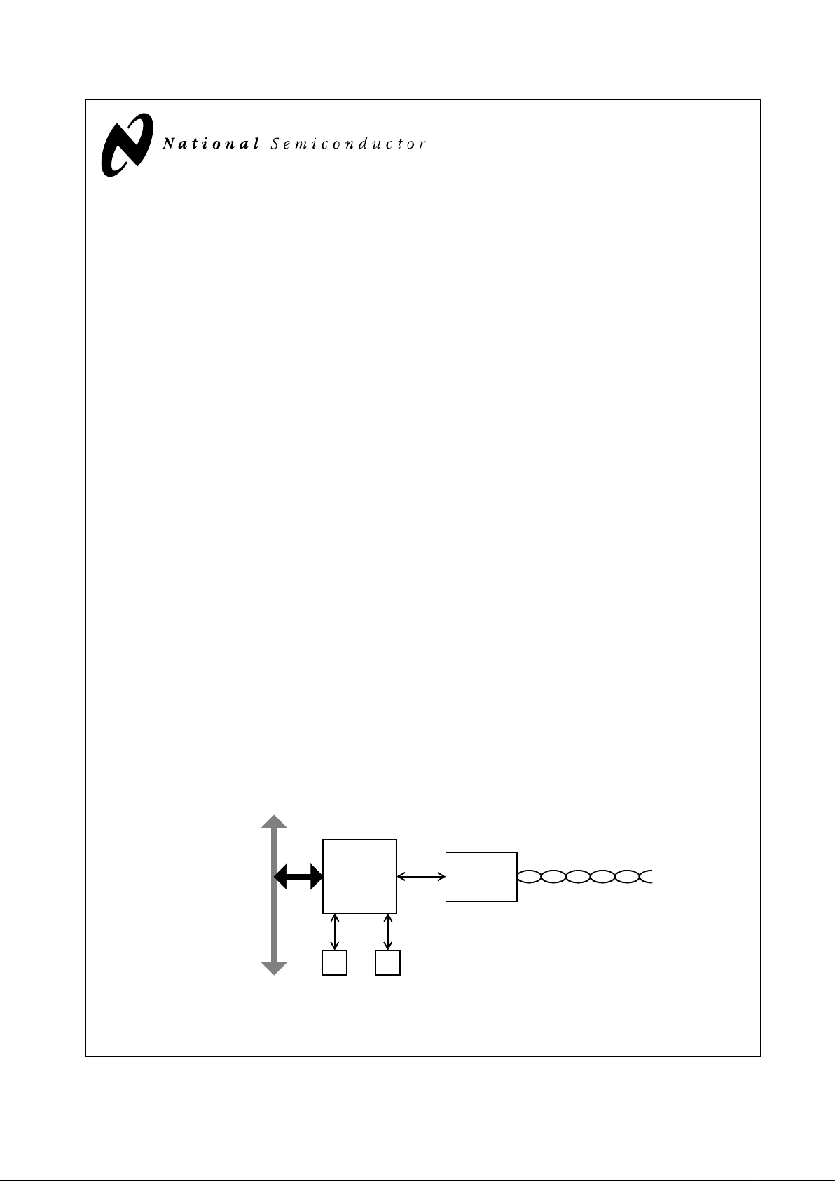
System Diagram
PCI Bus
DP83815
EEPROM
Isolation
10/100 Twisted Pair
BIOS ROM
(optional)
(optional)
Page 2

2 www.national.com
Table of Contents
1.0 Connection Diagram . . . . . . . . . . . . . . . . . . 4
2.0 Pin Description . . . . . . . . . . . . . . . . . . . . . . 5
3.0 Functional Description . . . . . . . . . . . . . . . 11
3.1 MAC/BIU . . . . . . . . . . . . . . . . . . . . . . . . . 12
3.1.1 PCI Bus Interface . . . . . . . . . . . . . . . . . . . . . . . . . . 12
3.1.2 Tx MAC . . . . . . . . . . . . . . . . . . . . . . . . . . . . . . . . . 13
3.1.3 Rx MAC . . . . . . . . . . . . . . . . . . . . . . . . . . . . . . . . . 13
3.2 Buffer Management . . . . . . . . . . . . . . . . . 13
3.2.1 Tx Buffer Manager . . . . . . . . . . . . . . . . . . . . . . . . . 13
3.2.2 Rx Buffer Manager . . . . . . . . . . . . . . . . . . . . . . . . . 13
3.2.3 Packet Recognition . . . . . . . . . . . . . . . . . . . . . . . . 13
3.2.4 MIB . . . . . . . . . . . . . . . . . . . . . . . . . . . . . . . . . . . . 14
3.3 Interface Definitions . . . . . . . . . . . . . . . . . 14
3.3.1 PCI System Bus . . . . . . . . . . . . . . . . . . . . . . . . . . . 14
3.3.2 Boot PROM . . . . . . . . . . . . . . . . . . . . . . . . . . . . . . 14
3.3.3 EEPROM . . . . . . . . . . . . . . . . . . . . . . . . . . . . . . . . 14
3.3.4 Clock . . . . . . . . . . . . . . . . . . . . . . . . . . . . . . . . . . . 14
3.4 Physical Layer . . . . . . . . . . . . . . . . . . . . . 16
3.4.1 Auto-Negotiation . . . . . . . . . . . . . . . . . . . . . . . . . . 16
3.4.2 Auto-Negotiation Register Control . . . . . . . . . . . . . 16
3.4.3 Auto-Negotiation Parallel Detection . . . . . . . . . . . . 16
3.4.4 Auto-Negotiation Restart . . . . . . . . . . . . . . . . . . . . 17
3.4.5 Enabling Auto-Negotiation via Software . . . . . . . . 17
3.4.6 Auto-Negotiation Complete Time . . . . . . . . . . . . . . 17
3.5 LED Interfaces . . . . . . . . . . . . . . . . . . . . . 17
3.6 Half Duplex vs. Full Duplex . . . . . . . . . . . 18
3.7 Phy Loopback . . . . . . . . . . . . . . . . . . . . . 18
3.8 Status Information . . . . . . . . . . . . . . . . . . 18
3.9 100BASE-TX TRANSMITTER . . . . . . . . . 18
3.9.1 Code-group Encoding and Injection . . . . . . . . . . . 19
3.9.2 Scrambler . . . . . . . . . . . . . . . . . . . . . . . . . . . . . . . 19
3.9.3 NRZ to NRZI Encoder . . . . . . . . . . . . . . . . . . . . . . 20
3.9.4 Binary to MLT-3 Convertor / Common Driver . . . . 20
3.10 100BASE-TX Receiver . . . . . . . . . . . . . . 21
3.10. 1 Input and Base Line Wander Compensation . . . .21
3.10.2 Signal Detect . . . . . . . . . . . . . . . . . . . . . . . . . . . . 21
3.10.3 Digital Adaptive Equalization . . . . . . . . . . . . . . . . 21
3.10.4 Line Quality Monitor . . . . . . . . . . . . . . . . . . . . . . . 24
3.10.5 MLT-3 to NRZI Decoder . . . . . . . . . . . . . . . . . . . .24
3.10.6 Clock Recovery Module . . . . . . . . . . . . . . . . . . . . 25
3.10.7 NRZI to NRZ . . . . . . . . . . . . . . . . . . . . . . . . . . . . . 25
3.10.8 Serial to Parallel . . . . . . . . . . . . . . . . . . . . . . . . . . 25
3.10.9 De-scrambler . . . . . . . . . . . . . . . . . . . . . . . . . . . . 25
3.10.10 Code-group Alignment . . . . . . . . . . . . . . . . . . . . 25
3.10.11 4B/5B Decoder . . . . . . . . . . . . . . . . . . . . . . . . . . 25
3.10.12 100BASE-TX Link Integrity Monitor . . . . . . . . . . 25
3.10.13 Bad SSD Detection . . . . . . . . . . . . . . . . . . . . . . 25
3.11 10BASE-T Transceiver Module . . . . . . . . 25
3.11.1 Operational Modes . . . . . . . . . . . . . . . . . . . . . . . . 25
3.11.2 Smart Squelch . . . . . . . . . . . . . . . . . . . . . . . . . . . 26
3.11.3 Collision Detection . . . . . . . . . . . . . . . . . . . . . . . . 26
3.11.4 Normal Link Pulse Detection/Generation . . . . . . . 26
3.11.5 Jabber Function . . . . . . . . . . . . . . . . . . . . . . . . . . 26
3.11.6 Automatic Link Polarity Detection . . . . . . . . . . . . . 26
3.11.7 10BASE-T Internal Loopback . . . . . . . . . . . . . . . . 27
3.11.8 Transmit and Receive Filtering . . . . . . . . . . . . . . . 27
3.11.9 Transmitter . . . . . . . . . . . . . . . . . . . . . . . . . . . . . . 27
3.11.10 Receiver . . . . . . . . . . . . . . . . . . . . . . . . . . . . . . . 27
3.11.11 Far End Fault Indication . . . . . . . . . . . . . . . . . . . 27
4.0 Register Set . . . . . . . . . . . . . . . . . . . . . . . . 28
4.1 Configuration Registers . . . . . . . . . . . . . . 28
4.1.1 Configuration Identification Register . . . . . . . . . . . 28
4.1.2 Configuration Command and Status Register . . . . 29
4.1.3 Configuration Revision ID Register . . . . . . . . . . . 30
4.1.4 Configuration Latency Timer Register . . . . . . . . . 31
4.1.5 Configuration I/O Base Address Register . . . . . . . 31
4.1.6 Configuration Memory Addr ess Register . . . . . . . 32
4.1.7 Configuration Subsystem Ident ification Register . 32
4.1.8 Boot ROM Configuration Register . . . . . . . . . . . . 33
4.1.9 Capabilities Pointer Register . . . . . . . . . . . . . . . . 33
4.1.10 Configuration Interrupt Select Register . . . . . . . . 34
4.1.11 Power Management Capabilities Register . . . . . 34
4.1.12 Power Management Control and Status Register 35
4.2 O perat ional Registers . . . . . . . . . . . . . . .36
4.2.1 Command Register . . . . . . . . . . . . . . . . . . . . . . . . 37
4.2.2 Configuration and Media Status Register . . . . . . . 38
4.2.3 EEPROM Access Register . . . . . . . . . . . . . . . . . . 40
4.2.4 EEPROM Map . . . . . . . . . . . . . . . . . . . . . . . . . . . 40
4.2.5 PCI Test Control Register . . . . . . . . . . . . . . . . . . . 41
4.2.6 Interrupt Status Register . . . . . . . . . . . . . . . . . . . . 42
4.2.7 Interrupt Mask Register . . . . . . . . . . . . . . . . . . . . 43
4.2.8 Interrupt Enable Register . . . . . . . . . . . . . . . . . . . 45
4.2.9 Transmit Descriptor Pointer Register . . . . . . . . . . 45
4.2.10 Transmit Configuration Register . . . . . . . . . . . . . 46
4.2.11 Receive Descriptor Pointer Register . . . . . . . . . . 47
4.2.12 Receive Configuration Register . . . . . . . . . . . . . 48
4.2.13 CLKRUN Control/Status Register . . . . . . . . . . . . 49
4.2.14 Wake Command/Status Register . . . . . . . . . . . . 51
4.2.15 Pause Control/Status Register . . . . . . . . . . . . . . 53
4.2.16 Receive Filter/Match Control Register . . . . . . . . 54
4.2.17 Receive Filter/Match Data Register . . . . . . . . . . 55
4.2.18 Receive Filter Logic . . . . . . . . . . . . . . . . . . . . . . 56
4.2.19 Boot ROM Address Register . . . . . . . . . . . . . . . . 60
4.2.20 Boot ROM Data Register . . . . . . . . . . . . . . . . . . 60
4.2.21 Silicon Revision Register . . . . . . . . . . . . . . . . . . 60
4.2.22 Management Information Base Control Register 61
4.2.23 Management Inf ormation Base Registers . . . . . . 62
4.3 Internal PHY Registers . . . . . . . . . . . . . . .63
4.3.1 Basic Mode Control Register (BMCR) . . . . . . . . . 63
4.3.2 Basic Mode Status Register (BMSR) . . . . . . . . . . 64
4.3.3 PHY Identifier Register #1 (PHYIDR1) . . . . . . . . . 65
4.3.4 PHY Identifier Register #2 (PHYIDR2) . . . . . . . . . 66
4.3.5 Auto-Negotiation Advertisement Register (ANAR) 66
4.3.6 Auto-Neg Link Partner Ability Reg (ANLPAR) . . . 67
4.3.7 Auto-Negotiate Expansion Register (ANER) . . . . 68
4.3.8 Auto-Neg Next Page Transmit Reg (ANNPTR) . . 68
4.3.9 PHY Status Register (PHYSTS) . . . . . . . . . . . . . . 69
4.3.10 MII Interrupt Control Register (MICR) . . . . . . . . . 71
4.3.11 MII Interrupt Status and Misc. Cntrl Reg (MISR) 71
4.3.12 False Carrier Sense Counter Register (FCSCR) 72
4.3.13 Receiver Error Counter Register (RECR) . . . . . . 72
4.3.14 100 Mb/s PCS Config and Status Reg (PCSR) . 72
4.3.15 PHY Control Register (PHYCR) . . . . . . . . . . . . . 73
4.3.16 10BASE-T Status/Control Register (TBTSCR) . . 74
4.4 Re comm ende d Registers Configuration .75
5.0 Buffer Management . . . . . . . . . . . . . . . . . .76
5.1 Overview . . . . . . . . . . . . . . . . . . . . . . . . .76
5.1.1 Descriptor Format . . . . . . . . . . . . . . . . . . . . . . . . . 76
5.1.2 Single Descriptor Packets . . . . . . . . . . . . . . . . . . 78
5.1.3 Multiple Descriptor Packets . . . . . . . . . . . . . . . . . 79
5.1.4 Descriptor Lists . . . . . . . . . . . . . . . . . . . . . . . . . . . 79
5.2 Transmit Architecture . . . . . . . . . . . . . . . .80
5.2.1 Transmit State Machine . . . . . . . . . . . . . . . . . . . . 80
5.2.2 Transmit Data Flow . . . . . . . . . . . . . . . . . . . . . . . 82
5.3 Receive Architecture . . . . . . . . . . . . . . . .83
5.3.1 Receive State Machine . . . . . . . . . . . . . . . . . . . . . 83
5.3.2 Receive Data Flow . . . . . . . . . . . . . . . . . . . . . . . . 85
6.0 DC and AC Specifications. . . . . . . . . . . . .86
Page 3

3 www.national.com
List of Figures
Figure 3-1 DP83815 Functional Block Diagram . . . . . . . . . . . . . . . . . . . . . . . . . . . . . . . . . . . . . . 11
Figure 3-2 MAC/BIU Functional Block Diagram . . . . . . . . . . . . . . . . . . . . . . . . . . . . . . . . . . . . . . 12
Figure 3-3 Ethernet Packet Format. . . . . . . . . . . . . . . . . . . . . . . . . . . . . . . . . . . . . . . . . . . . . . . . 14
Figure 3-4 DSP Physical Layer Block Diagram. . . . . . . . . . . . . . . . . . . . . . . . . . . . . . . . . . . . . . . 15
Figure 3-5 LED Loading Example. . . . . . . . . . . . . . . . . . . . . . . . . . . . . . . . . . . . . . . . . . . . . . . . . 17
Figure 3-6 100BASE-TX Transmit Block Diagram . . . . . . . . . . . . . . . . . . . . . . . . . . . . . . . . . . . . 19
Figure 3-7 Binary to MLT-3 conversion. . . . . . . . . . . . . . . . . . . . . . . . . . . . . . . . . . . . . . . . . . . . . 20
Figure 3-8 100 M/bs Receive Block Diagram . . . . . . . . . . . . . . . . . . . . . . . . . . . . . . . . . . . . . . . . 22
Figure 3-9 100BASE-TX BLW Event Diagram . . . . . . . . . . . . . . . . . . . . . . . . . . . . . . . . . . . . . . . 23
Figure 3-10 EIA/TIA Attenuation vs. Frequency for 0, 50, 100, 130 & 150 meters of CAT V cable 24
Figure 3-11 MLT-3 Signal Measured at AII after 0 meters of CAT V cable. . . . . . . . . . . . . . . . . . . 24
Figure 3-12 MLT-3 Signal Measured at AII after 50 meters of CAT V cable. . . . . . . . . . . . . . . . . . 24
Figure 3-13 MLT-3 Signal Measured at AII after 100 meters of CAT V cable. . . . . . . . . . . . . . . . . 24
Figure 3-14 10BASE-T Twisted Pair Smart Squelch Operation . . . . . . . . . . . . . . . . . . . . . . . . . . . 26
Figure 4-1 Pattern Buffer Memory -180h words (word=18bits). . . . . . . . . . . . . . . . . . . . . . . . . . . 57
Figure 4-2 Hash Table Memory - 40h bytes addressed on word boundaries. . . . . . . . . . . . . . . . 59
Figure 5-1 Single Descriptor Packets . . . . . . . . . . . . . . . . . . . . . . . . . . . . . . . . . . . . . . . . . . . . . . 78
Figure 5-2 Multiple Descriptor Packets. . . . . . . . . . . . . . . . . . . . . . . . . . . . . . . . . . . . . . . . . . . . . 79
Figure 5-3 List and Ring Descriptor Organization. . . . . . . . . . . . . . . . . . . . . . . . . . . . . . . . . . . . . 79
Figure 5-4 Transmit Architecture . . . . . . . . . . . . . . . . . . . . . . . . . . . . . . . . . . . . . . . . . . . . . . . . . 80
Figure 5-5 Transmit State Diagram. . . . . . . . . . . . . . . . . . . . . . . . . . . . . . . . . . . . . . . . . . . . . . . . 82
Figure 5-6 Receive Architecture . . . . . . . . . . . . . . . . . . . . . . . . . . . . . . . . . . . . . . . . . . . . . . . . . . 83
Figure 5-7 Receive State Diagram . . . . . . . . . . . . . . . . . . . . . . . . . . . . . . . . . . . . . . . . . . . . . . . . 85
List of Tables
Table 3-1 4B5B Code-Group Encoding/Decodi ng. . . . . . . . . . . . . . . . . . . . . . . . . . . . . . . . . . . . 20
Table 4-1 Configuration Register Map. . . . . . . . . . . . . . . . . . . . . . . . . . . . . . . . . . . . . . . . . . . . . 28
Table 4-2 Operational Register Map . . . . . . . . . . . . . . . . . . . . . . . . . . . . . . . . . . . . . . . . . . . . . . 36
Table 4-3 MIB Registers . . . . . . . . . . . . . . . . . . . . . . . . . . . . . . . . . . . . . . . . . . . . . . . . . . . . . . . 62
Table 5-1 DP83815 Descriptor Format . . . . . . . . . . . . . . . . . . . . . . . . . . . . . . . . . . . . . . . . . . . . 76
Table 5-2 cmdsts Common Bit Definitions. . . . . . . . . . . . . . . . . . . . . . . . . . . . . . . . . . . . . . . . . . 76
Table 5-3 Transmit Status Bit Definitions . . . . . . . . . . . . . . . . . . . . . . . . . . . . . . . . . . . . . . . . . . 77
Table 5-4 Receive Status Bit Definitions . . . . . . . . . . . . . . . . . . . . . . . . . . . . . . . . . . . . . . . . . . 78
Table 5-5 Transmit State Tables . . . . . . . . . . . . . . . . . . . . . . . . . . . . . . . . . . . . . . . . . . . . . . . . . 81
Table 5-6 Receive State Tables . . . . . . . . . . . . . . . . . . . . . . . . . . . . . . . . . . . . . . . . . . . . . . . . . 84
Page 4

4 www.national.com
1.0 Connection Diagram
Order Number DP83815VNG
See NS Package Number VNG14 4A
121
122
123
124
125
126
127
128
129
130
131
132
99
98
97
96
95
94
93
92
91
90
89
88
87
86
85
84
83
82
81
80
79
78
77
76
75
74
73
66
65
64
63
62
61
60
59
58
57
56
55
54
53
52
51
50
49
48
47
46
45
44
43
42
41
123456789
10
11
12
13
14
15
16
17
18
19
20
21
22
23
24
25
26
27
28
30
31
323329
Identification
Pin1
37
38
39
40
120
119
118
117
116
115
114
113
112
110
109
111
DEVSELN
TRDYN
IRDYN
FRAMEN
CBEN2
AD16
AD17
AD18
STOPN
PERRN
SERRN
PAR
CBEN1
AD15
AD14
AD13
AD12
AD11
AD10
AD9
PCIVSS4
AD8
AD19
AD20
AD21
AD22
AD23
IDSEL
PCIVSS2
PCIVDD3
VSSIO4
PCIVDD4
VDDIO4
PCIVSS3
PCIVDD2
CBEN3
AD24
AD25
AD26
CBEN0
MACVSS1
MACVDD1
RESERVED
VREF
PCIVDD1
AD29
AD31
PCIVSS1
REQN
GNTN
RSTN
INTAN
AD28
PCICLK
AD30
PMEN/CLKRUNN
TXIOVSS2
TXIOVSS1
TPTDP
TPTDM
NC
RXAVDD2
RXAVSS2
TPRDP
TPRDM
SUBGND2
AD27
AD7
AD6
AD5
PCIVSS5
MA1/LED10N
MA2/LED100N
MA3/EEDI
MA4/EECLK
MA5
MWRN
MD4/EEDO
MD3
EESEL
AD0
AD1
AD2
AD3
AD4
MD0
MCSN
MD1/CFGDISN
MD2
MD5
MD6
MD7
MA0/LEDACTN
PCIVDD5
VSSIO2
VDDIO2
MACVSS2
MACVDD2
VDDIO5
VSSIO5
MDIO
MDC
RXCLK
RXD0/MA6
RXD1/MA7
RXD2/MA8
RXD3/MA9
RXOE
RXER/MA10
RXDV/MA11
TXD3/MA15
COL/MA16
CRS
TXEN
TXCLK
TXD2/MA14
TXD1/MA13
TXD0/MA12
VSSIO3
VDDIO3
VSSIO1
VDDIO1
X2
X1
DP83815
SUBGND3
PHYVSS1
PHYVDD1
NC
3VAUX
363534
67
68
69
70
71
72
100
101
102
103
104
105
106
107
108
144
143
142
141
140
139
138
137
136
135
134
133
RXAVSS1
RXAVDD1
PWRGOOD
MRDN
TXDVDD
FXVDD
FXVSS
PHYVSS2
PHYVDD2
SUBGND1
RESERVED
NC
NC
RESERVED
TXDVSS
Page 5

5 www.national.com
2.0 Pin Description
PCI Bus Interface
Symbol Pin No(s) Direction Descripti on
AD[31-0 ] 66, 67 , 6 8, 7 0,
71, 72, 73, 74,
78, 79, 81, 82,
83, 86, 87, 88,
101, 10 2, 104 ,
105, 10 6, 108 ,
109, 11 0, 112 ,
113, 11 5, 116 ,
118, 11 9, 120 ,
121
I/O
Address and Data:
Multipl exed address an d da ta bus. As a bus ma s t er, the
DP83815 will drive address during the first bus phase. During subsequent
phases, the DP83815 w ill either read or write data ex pecting the target to
increm ent its address pointer. As a bus target, the DP83815 will decode ea ch
address on the bus and respond if it is the target being addressed.
CBEN[3-0] 75,89,100,111 I/O
Bus Command/Byte Enable:
During the address phase these signals define
the “b us com man d” o r t he type of bus tr an sac ti o n tha t wil l ta k e pl ace. D uri ng the
data phase these pins indicate which byte lanes contain valid data. CBEN[0]
applies to byte 0 (bits 7-0) and CBEN[3] applies to byte 3 (bits 31-24) in the
Little Endian Mode. In Big Endian Mode, CBEN[0] applies to byte 0 (bits 31-24)
and CBEN[3] applies to byte 3 (bits 7-0 ).
PCICLK 60 I
Clock:
This PCI Bus clock provi des timing for all bus phases . The risi ng edge
defines the start of each phase. Th e clock frequency ranges from 0 to 33 MHz.
DEVSELN 95 I/O
Device Select:
As a target, the DP83815 asserts this signal low when it
recognizes its address after FRAMEN is asserted. As a bus master, the
DP83815 samples this signal to insure that the destination address for the data
transfer is recognized by a PCI target.
FRAMEN 91 I/O
Frame:
As a bus master, this signal is asserted low to indicate the beginning
and duration of a bus transaction. Data transfer tak es place when this signal is
asserted. It is de-asserted before the transaction is in its final phase. As a
target, the device monitors this signal before decoding the address to check if
the current transaction is addressed to it.
GNTN 63 I
Grant:
This signal is asserted low to ind icate to the DP83815 that it has been
granted ownership of the bus by the central arbiter. This input is used when the
DP83815 is acting as a bus master.
IDSEL 76 I
Initialization Device Select:
This pin is sampled by the DP83815 to identify
when configuration re ad and write accesses are intended for it.
INT AN 61 O
Interrupt A:
This signal is asserted low w hen an interrupt condition as defined
in the Interrupt Status Register, In terrupt Mask, and I nterrupt Enabl e registers
occurs.
IRDYN 92 I/O
Initiator Ready:
As a bus master, this signal will be asserted low when the
DP83815 is ready to complete the current data phase transaction. This signal is
used in conjunction with the TRYDN signal . Data transaction takes place at the
rising edge of PCICLK when both IRDYN and TRDYN are asserted low. As a
target, this signal indicates that the master has put the data on the bus.
PAR 99 I/O
Parity:
This signal indicates even parity across AD[31-0] and CBEN[3-0]
includ ing the PAR pin. As a master, PAR is asserte d during address and write
data phases. As a target, PAR is asserted during read data phases.
PERRN 97 I/O
Parity Error:
The DP83815 as a master or target w ill assert this signal low to
indica te a pa rity er ror o n any in com in g d ata ( exc ep t f or sp ec ial c ycl e s) . As a bus
master, it will monitor this signal on all write operati ons (except for special
cycles).
REQN 64 O
Request:
The DP83815 will assert this signal low to request the owne rship of
the bus to the central arbiter.
RSTN 62 I
Reset:
When this signa l is asserted all outputs of DP83815 will be tri -stated
and the devic e will be put into a known state.
Page 6

6 www.national.com
2.0 Pin Description
(Continued)
SERRN 98 I/O
System Error:
This signal is asserted low by DP83815 during address parity
errors and system errors if enabled.
STOPN 96 I/O
Stop:
This signal is ass erted low by the target device to request the master
devi ce to stop the curr ent transacti on.
TRDYN 93 I/O
Target Ready:
As a target, this signal will be asserted low when the (sl ave )
device is ready to complete the current data phase transaction. This signal is
used in conjunct ion wit h the IRDYN signal. Data transaction takes place at the
rising edge of PCICLK when both IRDYN and TRDYN are asserted low. As a
master, this signal indicates that the targe t is ready for the data during writ e
operation and with the data during read operation.
PMEN/
CLKRUNN
59 I/O
Power Management Event/Clock Run Function:
This pin is a dual function
pin. The function of this pin is determined by the CLKRUN_EN bit 0 of the
CLKRUN Control and Status register (CCSR). This pin comes up with the
PMEN function selected.
Power Management Event:
This signal is asserted low by DP83815 to indicate
that a power management event has occurred.
Clock Run Function:
In this mode, this pin is used to indicate when the
PCICLK will be stopped.
3VAUX 122 I
PCI Aux Voltage Sense:
This pin is used to sense the presence of a 3.3v
auxili ary supply in order to define the PME Support available.
This pin has an internal weak pull down.
PWRGOOD 123 I
PCI bus power good:
Connected to PCI bus 3.3v power, this pin is used to
sense th e presence of PCI b us power during the D3 power management state.
This pin has an internal weak pull down.
Media Independent Interface (MII) - For Test Purposes Only.
Symbol Pin No(s) Direction Description
COL 28 I
Collision Detect:
The COL signal is asserted high asynchronously by the
external PMD upon detection of a collision on the medium. It will remain
asserted as long as the collision condition persists.
CRS 29 I
Carrier Sense:
This signal is asserted high asynch ronously by the external
physical un it up on detectio n of a non - id le med iu m .
MDC 5 O
Management Data Clock:
Clock signal with a maximum rate of 2.5 MHz used
to transfer management data for the external PMD on the MDIO pin.
MDIO 4 I/O
Management Data I/O:
Bidirectiona l signal used to transfer management
inf ormation for the external PMD. Requires an external 4.7 KΩ pullup resisto r.
RXCLK 6 I
Receive Clock:
A continuous clock, sourced by an external PMD device, that is
recovered from the incoming data. During 100 Mb/s operation RX_CLK is 25
MHz and duri ng 10 Mb/s this is 2.5 MHz.
RXD3/MA9,
RXD2/MA8,
RXD1/MA7,
RXD0/MA6
12, 11, 10, 7 I
O
Receive Data
: This is a group of 4 signals, sourced from an external PMD, that
conta in s da t a al ig ne d on nibble boundaries and are dr iven syn c hr o no us to t he
RX_CLK. RXD[3] is the most significant bit and RXD[0] is the least sign ificant
bit.
BIOS ROM Address:
During external BIOS ROM access, these signals
become part of the R OM address.
PCI Bus Interface
Symbol Pin No(s) Direction Descripti on
Page 7

7 www.national.com
2.0 Pin Description
(Continued)
RXDV/MA11 15 I
O
Receive Data Valid:
This indicates that the external PMD is presenting
recovered and decoded nibbles on the RXD sign als, and that RX_CLK is
synchronous to the recovered data in 100Mps operation. This si gnal will
encompass the frame, starting with the Start-of-Frame delimiter (JK) and
excluding an y End-of-Frame delimiter (TR).
BIOS ROM Address:
During external BIOS ROM access, this signal becomes
part of the ROM address.
RXER/MA10 14 I
O
Receive Error:
This signal is asserted high synchronously by the external PMD
whenever it detects a media error and RXDV is asserted in 100Mps operation.
BIOS ROM Address:
During external BIOS ROM access, this signal becomes
part of the ROM address.
RXOE 13 O
Receive Output Enable:
This pin is used to disable an external PMD while th e
BIOS ROM is being accessed.
TXCLK 31 I
Transmit Clock:
A continuous clock that is sourced by the external PMD.
During 100 Mb/s operation this is 25 MHz +/- 100 ppm. During 10 Mb/s
operation thi s clock is 2.5 MHz +/- 100 ppm.
TXD3/MA15,
TXD2/MA14,
TXD1/MA13,
TXD0/MA12
25, 24, 23, 22 O
O
Transmit Data:
This is a group of 4 data signal s which are driven synchronous
to the T XCLK for transmission to th e external PMD. TXD [3] is the most
significant bit and TXD[0] is the least significant bit.
BIOS ROM Address:
During external BIOS ROM access, these signals
become part of the R OM address.
TXEN 30 O
Transmit Enable:
This signal is synchronous to TXCLK and provides precise
framing for data carried on TX D[3-0] for the exte rnal PMD. It is asserted when
TXD[3-0] contains valid data to be transmitted.
100BASE-TX/10BASE-T Interface
Symbol Pin No(s) Direction Description
TPTDP,
TPTDM
54, 53 A-O
Transmit Data:
Differential commo n output driver. This differential output is
configurable to either 10BASE-T or 100BASE-TX signaling:
10BASE-T: Transmission of Manchester encoded 10BASE-T packet data as
well as Link Pulses (including Fast Link Pulses for A uto-Negotiation purposes).
100BASE-TX: Transmission of ANS I X3T12 c ompliant MLT-3 data.
The DP83815 will automatically config ure this common output dri ver for the
proper signal type as a result of either forced configuration or Auto-Negotia tion.
TPRDP,
TPRDM
46, 45 A-I
Receive Data:
Different ial com m on input buffer. This diff erential input can be
configured to accept either 100BASE-TX or 10BASE-T signaling:
10BASE-T: Reception of Mancheste r encoded 10BASE-T pa cket data as well
as normal Link Puls es and Fast Link Pulses for Auto-Negotiation pu rposes.
100BASE-TX: Reception of ANSI X3T 12 compliant scrambled MLT-3 dat a.
The DP83815 will automatically configur e this common input buffer to accept
the proper signal type as a result of either fo rced configur ation or AutoNegotiation.
Media Independent Interface (MII) - For Test Purposes Only.
Symbol Pin No(s) Direction Description
Page 8

8 www.national.com
2.0 Pin Description
(Continued)
Note: DP83815 supports NM27LV010 for the ROM interface device.
BIOS ROM/Flash Interface
Symbol Pin No(s) Direction Description
MCSN 129 O
BIOS PROM/Flash Chip Select:
During a BIOS ROM/Flash ac cess, this
signal is used to select the ROM device.
MD7, MD6, MD5,
MD4/EEDO, MD3,
MD2,
MD1/CFGDISN,
MD0
141, 140, 139,
138, 135, 134,
133, 13 2
I/O
BIOS ROM/Flash Data Bus:
During a BIOS ROM/Flash access these
signals are used to transfer data to or from the ROM/Flash device.
MD[5:0] and MD7 pins have an internal weak pull up.
MD6 pin has an internal weak pull down.
MA5, MA 4/EECLK ,
MA3/EEDI,
MA2/LE D100LNK,
MA1/LE D10LNK,
MA0/LE DACT
3, 2, 1, 144,
143, 14 2
O
BIOS ROM/Flash Address:
During a BIOS ROM/Flash access, these
signal s are used to drive the ROM/Flash address.
MWRN 131 O
BIOS ROM/Flash Write:
During a BIOS ROM/Flash access, this signal is
used to e nable data to be written to the Fl ash de vice.
MRDN 130 O
BIOS ROM/Flash Read:
During a BIOS ROM/Flash access, this signal is
used to enable data to be read from the Flash device.
Clock Interface
Symbol Pin No(s) Direction Description
X1 17 I
Crystal/Oscillator Input:
This pin is the primary clock reference input for the
DP83815 IC an d mus t be co nn ecte d t o a 25MH z 0.0 05 % (50 pp m) c loc k s our c e .
The DP83815 de vice supports either an external crystal resonator connected
across pins X1 and X2, or an external CMOS-level oscillator source connected
to pin X1 only.
X2 18 O
Crystal Output:
This pin is used in conjunction wi th the X1 p in to connect to an
external 25MHz crystal resonator device. This pin must be left unconnected if
an ext ernal CMOS oscillator cloc k source is utilized. For more information see
the definition for pin X1.
LED Interface
Symbol Pin No(s) Direction Description
LEDACTN/MA0 142 O
TX/RX Activity:
This pin is an output indicating transmit/receive activity. This
pin is d riv en l o w to i ndica t e a ctive transmissi on or r ec ep tio n, an d can be use d t o
drive a low current LED (<4mA). The activity event is stretched to a minimum
duration of approximately 50ms.
LED100N/MA2 144 O
100Mb/s Link:
This pi n i s a n out pu t in dica ti ng t he 1 00M b/s Li nk st atus . T hi s p in
is driven low t o indicate Good Link status for 100Mb/s operation, and can be
used to d rive a low current LED (<4mA).
LED10N/MA1 143 O
10Mb/s Link:
This pin is a n ou tp ut indi ca ti n g th e 1 0Mb /s Li nk sta tu s . T hi s pi n is
driven low to indicate Good Link status for 10Mb/s operation, and can be used
to drive a low current LED (<4mA).
Page 9

9 www.national.com
2.0 Pin Description
(Continued)
Note: DP83815 supports NMC93C46 for the EEPROM device.
Serial EEPROM Interface
Symbol Pin No(s) Direction Description
EESEL 128 O
EEPROM Chip Select:
This signal is used to enable the external EEPROM
device.
EECLK/MA4 2 O
EEPROM Clock:
During an EEPROM access (EESEL asserted), this pin is an
output used to drive the serial clock to an external EEPROM device.
EEDI/MA3 1 O
EEPROM Data In:
During an EEPROM access (EESEL asserted), this pin is
an outp ut used to dr ive opcode, address, and data to an external serial
EEPROM device.
EEDO/MD4 138 I
EEPROM Data Out:
During an EEPROM access (EESEL asserted), this pin is
an input used to retrieve EEPROM serial read data.
This pin has an internal weak pull up .
MD1/CFGDISN 133 I/O
Configuration Disable:
When pulled low at power-on time, disables load of
configuration data from the EEPROM. Use 1 KΩ to ground to disable cfg. load.
External Referen ce Inte rface
Symbol Pin No(s) Direction Description
VREF 40 I
Bandgap Reference:
External current reference resistor for internal Phy
bandga p circuitry. The value of this resistor is 9.31 KΩ 1% metal film
(100ppm/
o
C) which must be connected from the VREF pin to analog ground.
Supply Pins
Symbol Pin No(s) Direction Description
SUBGND1,
SUBGND2,
SUBGND3
37, 49, 126 S Substrate GND
RXAVDD1,
RXAVDD2
39, 47 S RX Analog VDD - connect to isolated Aux 3.3v supply VDD
RXAVSS1,
RXAVSS2
38, 44 S RX Analog GND
TXIOVSS1,
TXIOVSS2
52, 55 S TX Output driver VS S
TXDVDD 56 S TX Digital VDD - connec t to Aux 3.3v supply VDD
TXDVSS 51 S TX Digital VSS
MACVDD1,
MACVDD2
58,125 S Mac/BIU digital core VDD - connect to Aux 3.3v supply VDD
MACVSS1,
MACVSS2
57, 124 S Mac/BIU digital core VSS.
Page 10

10 www.national.com
2.0 Pin Description
(Continued)
PCIVDD1,
PCIVDD2,
PCIVDD3,
PCIVDD4,
PCIVDD5
69, 80, 94,
107, 11 7
S PCI IO VDD - connect to PCI bus 3.3v VDD
PCIVSS1,
PCIVSS2,
PCIVSS3,
PCIVSS4,
PCIVSS5
65, 77, 90,
103, 11 4
S PCI IO VSS
VDDIO2,
VDDIO4
19, 85 S Misc. IO VDD - connect to Aux 3.3v supply VDD
VDDIO1,
VDDIO3,
VDDIO5
9, 27, 137 S Misc. IO VDD - connect to Aux 3.3v supply VDD
VSSIO2,
VSSIO4
16, 84 S Misc. IO VSS
VSSIO1,
VSSIO3,
VSSIO5
8, 26, 13 6 S Misc. IO VSS
PHYVDD1,
PHYVDD2
21, 33 S Phy digita l core VDD - connect to Aux 3.3v supply VDD
PHYVSS1,
PHYVSS2
20,32 S Phy digital core VSS
FSVDD 36 S Frequency Synthesizer VDD - co nnect to isolated Aux 3.3v supply VDD
FSVSS 35 S Fr equency Synthesi zer VSS
No Connects
Symbol Pin No(s) Direction Description
NC 34, 42, 43, 48 No Connect
Reserved 41, 50 , 127 These pins are reserved a nd cannot be connected to any external lo gic or net.
Supply Pins
Symbol Pin No(s) Direction Description
Page 11
11 www.national.com
3.0 Functional Description
DP83815 consists of a MAC/BIU (Media Access
Controller/Bus Interface Unit), a physical layer interface,
SRAM, and miscellaneous support logic. The MAC/BIU
includes the PCI bus , BIOS ROM and EEPROM interfaces,
and an 802.3 MAC. The physical layer interface used is a
single-port version of the 3.3v DsPhyter. Internal memory
consists of on e - 0.5K B a nd two - 2K B SR A M blo cks.
Figure 3-1 DP83815 Functional Block Diagram
MAC/BIU
Interface
SRAM
25Mhz Clk
MII RX
MII TX
MII Mgt
BIOS ROM Cntl
BIOS ROM Data
BROM/EE
PCI AD
PCI CNTL
PCI CLK
3v DSP Physical Layer
Logic
RX-2KB
SRAM
TX-2KB
TPRDP/M
EEPROM/LEDs
MII TX
MII RX
MII Mgt
Test data in
Test data out
MII TX
MII RX
MII Mgt
TPTDP/M
DP83815
Tx Addr
Tx wr data
Rx Addr
Rx wr data
Rx rd data
Tx rd data
RAM
BIST
Logic
SRAM
RXFilter
.5KB
Page 12
3.0 Functional Description
(Continued)
12 www.national.com
Figure 3-2
MAC/BIU
Functional Block Diagram
3.1 MAC/BIU
The MAC/BIU is a derivative design from the DP83810
(Euphrates). The original MAC/BIU design has been
optimized to improve logic efficiency and enhanced to add
features consistent with current market needs. The
MAC/BIU des ign blocks are di scussed in this secti on.
3.1.1 PCI Bus Interface
This block implements PCI v2.2 bus protocols, and
configura ti on space. Supports bu s master reads and writes
to CPU memory, and CPU access to on-chip register
space. Additional functions provided include: configuration
control, serial EEPROM access with auto configuration
load, interrupt control, power management control with
support for PME or CLKRUN function.
3.1.1.1 Byte Ordering
The DP83815 can be configured to order the bytes of data
on the AD[31:0] bus to conf orm to little endian or b ig endian
ordering through the use of the CFG:BEM bit
(Configuration Register, bit 0). On Power-up, the device is
in little endian ordering. Byte ordering only affects data
FIFOs. Regis ter information remains bit aligned (i.e . AD[31]
maps to bit 31 in any register space, AD[0] maps to bit 0,
etc).
Tx Buffer Manager
MIB
Tx MAC
Rx MAC
PCI Bus
Data FIFO
Physical Layer Interface
93C06
Serial
EEPROM
MAC/BIU
32
15
32
32
32
32
32
16
32
32
4
4
32
Rx Filter
Pkt Recog
Logic
SRAM
Rx Buffer Manager
Data FIFO
Boot ROM/
Flash
PCI Bus
Interface
Page 13

3.0 Functional Description
(Continued)
13 www.national.com
Little Endian (CFG:BEM=0):
The byte orientation for
receive and transmit data and descriptors in system
memory is as follows:
Big Endian (CFG:BEM=1):
The byte orientation for
receive and transmit data and descriptors in system
memory is as follows:
3.1.1.2 PCI Bus Interr upt Control
PCI bus interrupts for the DP83815 are asynchronously
performed by asserting pin INTAN. This pin is an open
drain outp ut. The source o f t he interrupt can be determined
by reading the Interrupt Status Regis ter (ISR). One or more
bits in the ISR will be set, denoting all currently pending
interrupts.
Caution:
Reading of the ISR clears ALL bits.
Masking of specified interrupts can be accomplished by
using the Interrupt Mask Register (IMR).
3.1.1.3 Timer
The Latency Timer described in CFGLAT:LAT defines the
minimum number of bus clocks that the device will hold the
bus. Once the device gains control of the bus and issues
FRAMEN, the Latency Timer will begin counting down. If
GNTN is de-asserted before the DP83815 has finished
with the bus, the device will maintain ownership of the bus
until the timer reaches zero (or has finished the bus
transfer). The timer is an 8-b it counter .
3.1.2 Tx MAC
This block implements the transmit portion of 802.3 Media
Access Control. The Tx MAC retrieves packet data from the
Tx Buffer Manager and sends it out through the transmit
portion. Additionally, the Tx MAC provides MIB control
information for transmit packets .
3.1.3 Rx MAC
This block implements the receive portion of 802.3 Media
Access Control. The Rx MAC retrieves packet data from
the receive portion and sends it to the Rx Buffer Manager.
Additionally, the Rx MAC provides MIB control information
and packet address data for the Rx Filter .
3.2 Buffer Management
The buffer management scheme used on the DP83815
allows quick, simple and efficient use of the frame buffer
memory. Frames are saved in similar formats for both
transmit and receive. The buffer management scheme also
uses separate buffers and descriptors for packet
information. This allows effective transfers of data from the
receive buffer to the transmit buffer by simply transferring
the descriptor from the receive queue to the transmit
queue.
The format of the descriptors allows the packets to be
saved in a number of configurations. A packet can be
stored in memory with a single descriptor per single
packet, or multiple descriptors per single packet. This
flexibility allows the user to configure the DP83815 to
maximize efficiency. Architecture of the specific system’s
buffer memory, as well as the nature of network traffic, will
determine the most suitable configuration of packet
descriptors and fragments. Refer to the Buffer
Management Section for more information.
3.2.1 Tx Buffer Manager
This block DMAs packet data from PCI memory space and
places it in the 2KB transmit FIFO, and pulls data from the
FIFO to send to the Tx MAC. Multiple packets may be
present in the FIFO, al lowing pac kets to b e transmitted with
minimum interframe gap. The way in which the FIFO is
emptied and filled is controlled by the FIFO threshold
values in the TXCFG register: FLTH (Tx Fill Threshold),
DRTH (Tx Drain Threshold). These values determine how
full or empty the FIFO must be before the device requests
the bus. Additionally, once the DP83815 requests the bus,
it will attempt to empty or fill the FIFO as allowed by the
MXDMA setting in the TXCFG register.
3.2.2 Rx Buffer Manager
This block retrieves packet data from the Rx MAC and
places it in the 2KB receive data FIFO, and pulls data from
the FIFO for DMA to PCI memory space. The Rx Buffer
Manager maintains a status FIFO, allowing up to 4 packets
to reside in the FIFO at once. Similar to the transmit FIFO,
the receive FIFO is controlled by the FIFO threshold value
in the RXCFG register: DRTH (Rx Drain Threshold). This
value determines the number of long words written into the
FIFO from the MAC unit before a DMA request for system
memory access occurs. Once the DP83815 gets the bus, it
will continue to transfer the long words from the FIFO until
the data in the FIFO is less than one long word, or has
reached the end of the packet, or the max DMA burst size
is reached (RXCFG:MXDMA).
3.2.3 Packet Recognition
The Receive packet filter and recognition logic allows
software to control which packets are accepted based on
destination address and packet type. Address recognition
logic includes support for broadcast, multicast hash, and
unicast addresses. The packet recognition logic includes
Byte 0Byte 1Byte 2Byte 3
0781516
232431
LSB
C/BE[0]C/BE[1]C/BE[2]C/BE[3]
MSB
Byte 3Byte 2Byte 1Byte 0
0781516
232431
MSB
C/BE[0]C/BE[1]C/BE[2]C/BE[3]
LSB
Page 14

3.0 Functional Description
(Continued)
14 www.national.com
support for WOL, Pause, and programmable pattern
recognition.
The standard 802.3 Ethernet packet consists of the
following fields: Preamble (PA), Start of Frame Delimiter
(SFD), Destination Address (DA), Source Address (SA),
Length (LEN), Data and Fr ame Check Sequence (FCS). All
fields are fixed length except for the data field. During
reception, the PA, SFD and FCS are stripped. During
transmissi on, the DP83815 generates and appends t he PA,
SFD and FCS.
3.2.4 MIB
The MIB block contains counters to track certain media
events required by the management specifications RFC
1213 (MIB II), RFC 1398 (Ether-like MIB), and IEEE 802.3
LME. The counters provided are for events which are eithe r
difficult or impossible to be intercepted directl y by software.
Not all counters are implemented, however required
counters can be calculated from the counters provided.
3.3 Interface Definitions
3.3.1 PCI System Bus
This interface allows direct connection of the DP83815 to a
33MHz PCI system bus. The DP83815 supports zero wait
state data transfers with burst sizes up to 128 dwords. The
DP83815 conforms to 3.3V AC/DC specifications, but has
5V tolerant inputs.
3.3.2 Boot PROM
The BIOS ROM interface allows the DP83815 to read from
and write data to an external PROM /Flash device .
3.3.3 EEPROM
The DP83815 supports the attachment of an external
EEPROM. The EEPROM interface provides the ability for
the DP83815 to read from and write data to an external
serial EEPROM device. Values in the external EEPROM
allow default fields in PCI configuration space and I/O
space to be overridden following a hardware reset. The
DP83815 will auto-load values from the EEPROM to these
fields in configuration space and I/O space and perform a
checksum to verify that the data is valid. If the EEPROM is
not present, the DP83815 initialization uses default values
for the appropriate Configuration and Operational
Registers. Software can read and write to the EEPROM
using “bit-bang” accesses via the EEPROM Access
Register.
3.3.4 Clock
The clock interface provides the 25MHz clock reference
input for the DP83815 IC. This interface supports operation
from a 25MHz, 50 ppm CMOS oscillator, or a 25MHz, 50
ppm crystal resonator.
Figure 3-3 Ethernet Packet Format
60b 4b 6B 2B 46B-1500B 4B
FCSDataLENSADAPA6BSFD
Note: B = Bytes
b = bits
Page 15
3.0 Functional Description
(Continued)
15 www.national.com
Figure 3-4 DSP Physical Layer Block Diagram
TRANSMIT CHANNELS &
100 MB/S 10 MB/S
NRZ TO
MANCHESTER
ENCODER
STATE MACHINES
TRANSMIT
FILTER
LINK PULSE
GENERATOR
4B/5B
ENCODER
SCRAMBLER
PARALLEL TO
SERIAL
NRZ TO NRZI
ENCODER
BINARY TO
MLT-3
ENCODER
10/100 COMMON
RECEIVE CHANNELS &
100 MB/S 10 MB/S
MANCHESTER
TO NRZ
DECODER
STATE MACHINES
RECEIVE
FILTER
LINK PULSE
DETECTOR
4B/5B
DECODER
DESCRAMBLER
SERIAL TO
PARALLEL
NRZI TO NRZ
DECODER
MLT-3 TO
10/100 COMMON
AUTO-NEGOTIATION
STATE MACHINE
FAR-END-FAULT
STATE MACHINE
REGISTERS
AUTO
100BASE-X
10BASE-T
MII
BASIC MODE
PCS CONTROL
PHY ADDRESS
NEGOTIATION
CLOCK
CLOCK
RECOVERY
CLOCK
RECOVERY
CODE GROUP
ALIGNMENT
SMART
SQUELCH
RX_DATA
RX_CLK
RX_DATARX_CLK
TX_DATA
TX_DATA
TX_CLK
SYSTEM CLOCK
REFERENCE
RD
±
TD
±
OUTPUT DRIVER
INPUT BUFFER
BINARY
DECODER
ADAPTIVE
EQ
AND
BLW
COMP.
(ALSO FX_RD
±)
LED
DRIVERS
LEDS
HARDWARE
CONFIGURATION
PINS
GENERATION
(AN_EN, AN0, AN1)
CONTROL
NCLK_50M
TX_CLK
TXD(3:0)
TX_ER
TX_EN
MDIO
MDC
COL
CRS
RX_EN
RX_ER
RX_DV
RXD(3:0)
RX_CLK
MAC INTERFACE
SERIAL
MANAGEMENT
Page 16

3.0 Functional Description
(Continued)
16 www.national.com
3.4 P hysical Layer
The DP83815 has a full featured physical layer device with
integrated PMD sub-layers to support both 10BASE-T and
100BASE-TX Ethernet protocols. The physical layer is
designed for easy implementation of 10/100 Mb/s Ethernet
home or office solutions. It interfaces directly to twisted pair
media via an external transformer. The physical layer
utilizes on chip Digit al Signal Processing (DSP) technology
and digital PLLs for robust performance under all operating
conditions, enhanced noise immunity, and lower external
component count when com pared to analog solutions.
3.4.1 Auto-Negotiation
The Auto-Negotiation function provides a mechanism for
exchanging configuration inform ation between two ends of
a link segment and automatically selecting the highest
performance mode of operat ion supported by both devices.
Fast Link Pulse (FLP) Bursts provide the signalling used to
communicate Auto-Negotiation abilities between two
devices at each end of a link segment. For further detail
regarding Auto-Negotiation, refer to Clause 28 of the IEEE
802.3u specification. The DP83815 supports four different
Ethernet protocols (10 Mb/s Half Duplex, 10 Mb/s Full
Duplex, 100 Mb/s Half Duplex, and 100 Mb/s Full Duplex),
so the inclusion of Auto-Negotiation ensures that the
highest performance protocol will be selected based on the
advertised ability of the Link Partner. The Auto-Negotiation
function within the DP83815 is controlled by internal
register access. Auto-Negotiation will be set at powerup/reset, and also when a link status(up/valid) change
occurs.
3.4.2 Auto-Negotiation Register Control
When Auto-Negotiation is enabled, the DP83815 transmits
the abilities programmed into the Auto-Negotiation
Advertisement register (ANAR) via FLP Bursts. Any
combination of 10 Mb/s, 100 Mb/s, Half-Duplex, and Full
Duplex modes may be selected. The default setting of bits
[8:5] in the ANAR and bit 12 in the BMCR register are
dete rmined at pow e r -up.
The BMCR provides software with a mechanism to control
the operation of the DP83815. Bits 1 & 2 of the PHYSTS
register are only valid if Auto-Negotiation is disabled or
after Auto-Negotiation is complete. The Auto-Negotiation
protocol compares the contents of the ANLPAR and ANAR
registers and uses the results to automatically configure to
the highest performance protocol common to the local and
far-end port. The results of Auto-Negotiation may be
accessed in register C0h (PHYSTS), bit 4: AutoNegotiation Complete, bit 2: Duplex Status and bit 1:
Speed Status.
Auto-Negotiation Priority Resolution:
— (1) 100BASE-TX Full Duplex (Highest Priority)
— (2) 100BASE-TX Half Duplex
— (3) 10BASE-T Full Duplex
— (4) 10BASE-T Half Duplex (Lowest Priority)
The Basic Mode Control Register (BMCR) provides control
for enabling, disabling, and restarting the Auto-Negotiation
process. When Auto-Negotiation is disabled the Speed
Selection bit in the BCMR (bit 13) controls switching
between 10 Mb/s or 100 Mb/s operation, and the Duplex
Mode bit (bit 8) controls switching between full duplex
operation and half duplex operation. The Speed Selection
and Duplex Mode bits have no effect on the mode of
operation when the Auto-Negotiation Enable bit (bit 12) is
set.
The Basic Mode Status Register (BMSR) indicates the set
of available abilities for technology types, Auto-Negotiation
ability, and Extended Register Capability. These bits are
permanently set to indicate the full functionality of the
DP83815 (only the 100BASE-T4 bit is not set since the
DP83815 does not support that function).
The BMSR also provides st atus on:
— Whether Auto-Negotiation is complete (bit 5)
— W hether the Link Partner is advertising that a remote
fault has occurr ed (bit 4)
— Whether a valid lin k has been established (bit 2)
— Support for Management Frame Preamble suppression
(bit 6)
The Auto-Negotiation Advertisement Register (ANAR)
indicates the Auto-Negotiation abilities to be advertised by
the DP83815. All available abilities are transmitted by
default, bu t any a bilit y ca n be suppressed by writing to the
ANAR. Updating the ANAR to suppress an ability is one
way for a management agent to change (force) the
technology that is used.
The Auto-Negotiation Link Partner Ability Register
(ANLPAR) is used to receive the base link code word as
well as all next page code words during the negotiation.
Furthermore, the ANLPAR will be updated to either 0081h
or 0021h for parallel detection to either 100 Mb/s or 10
Mb/s respectively.
The Auto-Negotiation Expansion Register (ANER)
indicates additional Auto-Negotiation status. The ANER
provides status on:
— Whether a Parallel Detect Fault has occurred (bit 4)
— W hether the Link Partner supports the Next Page
function (bit 3)
— Whether the DP83815 supports the Next Page function
(bit 2). The DP83815 does support the Next Page
function.
— Whether the current page being exchanged by Auto-
Negotiation has been received (bit1)
— Whether the Link Partner supports Auto-Negotiation (bit
0)
3.4.3 Auto-Negotiation Parallel Detection
The DP83815 supports the Parallel Detection function as
defined in the IEEE 802.3u specification. Parallel Detection
requires both the 10 Mb/s and 100 Mb/s receivers to
monitor the receive signal and report link status to the
Auto-Negotiation function. Auto-Negotiation uses this
information to configure the correct technology in the event
that the Link P artner does not support Auto-Negotiation yet
is transmitting link signals that the 100BASE-TX or
10BASE-T PMAs (Physical Medium Attachments)
recognize as valid link si gnals.
If the DP83815 completes Auto-Negotiation as a result of
Parallel Detection, bits 5 and 7 within the ANLPAR register
will be updated to reflect the mode of operation present in
the Li nk Partner. Not e th a t b i ts 4 :0 o f th e A N L PAR will also
be set to 00001 based on a successful parallel detection to
indicate a valid 802.3 selector field. Software may
determine that negotiation completed via Parallel Detect ion
Page 17

3.0 Functional Description
(Continued)
17 www.national.com
by reading the ANER (98h) register with bit 0, Link Partner
Auto-Negotiation Able bit, being reset to a zero, once the
Auto-Negotiation Complete bit, bit 5 of the BMSR (84h)
register is set to a one. If configured for parallel detect
mode, and any condition other than a single good link
occurs, then the parallel detect fault bit will set to a one, bit
4 of the ANER register (98h).
3.4.4 Auto-Negotiation Restart
Once Auto-Negotiation has completed, it may be restarted
at any time by setting bit 9 (Restart Auto-Negotiation) of the
BMCR to one. If the mode configured b y a successful AutoNegotiation loses a valid link, then the Auto-Negotiation
process will resume and attempt to determine the
configuration for the link. This function ensures that a valid
configuration is maintained if the cable becomes
disconnected.
A renegotiation request from any entity, such as a
management agent, will cause the DP83815 to halt any
transmit data and link pulse activity until the
break_link_timer expires (~1500 ms). Consequently, the
Link Partner will go into link fail and normal AutoNegotiation resumes. The DP83815 will resume AutoNegotiation after the break_link_timer has expired by
issuing FLP (Fast Link Puls e) bursts.
3.4.5 Enabling Auto-Negotiation via Software
It is important to note that if the DP83815 has been
initialized upon power-up as a non-auto-negotiating device
(forced technology), and it is then required that AutoNegotiation or re-Aut o-Negotiation be initiated via software ,
bit 12 (Auto-Negotiation Enable) of the Basic Mode Control
Register must first be cleared and then set for any AutoNegotiation function to take effect.
3.4.6 Auto-Negotiation Complete Time
Parallel detection and Auto-Negotiation take approximately
2-3 seconds to complete. In addi tion, Auto-Negotiation with
next page should take approximately 2-3 seconds to
complete, depending on the number of next pages sent.
Refer to Clause 28 of the IEEE 802.3u standard for a full
description of the individual timers related to AutoNegotiation.
.
Figure 3-5 LED Loading Example
3.5 LED Interfaces
The DP83815 has parallel outputs to indicate the status of
Activity (Transmit or Receive), 100 Mb/s Link, and 10 Mb/s
Link.
The LEDACTN pin indicates the presence of transmit or
receive activity. The standard CMOS driver goes low when
RX or TX activity is detected in either 10 Mb/s or 100 Mb/s
operation.
The LED100N pin indicates a good link at 100 Mb/s data
rate. The standard CMOS driver goes low when this
occurs. In 100BASE-T mode, link is established as a result
of input receive amplitude compliant with TP-PMD
specifications which will result in internal generation of
signal detec t. This signal will a ssert af ter the int ernal Signal
Detect has remained asserted for a minimum of 500 us.
The signal will de-assert immediately following the deassertion of the internal signal detect.
The LED10N pin indic ates a good link at 10 Mb/s data rate.
The standard CMOS driver goes low when this occurs. 10
Mb/s Link is established as a result of the reception of at
least seven consecutive normal Link Pulses or the
reception of a valid 10BASE-T packet. This will cause the
assertion of this signal. the signal will de-assert in
accordance with the Link Loss Timer as specified in IEEE
802.3.
V
CC
LED10N
453
Ω
LEDACTN
453
Ω
LED100N
453
Ω
Page 18

3.0 Functional Description
(Continued)
18 www.national.com
3.6 Half Duplex vs. Full Duplex
The DP83815 supports both half and full duplex operation
at both 10 Mb/s and 100 Mb/s speeds.
Half-duplex is the standard, traditional mode of operation
which relies on the CSMA/CD protocol to handle collisions
and network access. In Half-Duplex mode, CRS responds
to both transmit and receive activity in order to maintain
compliance with IEEE 802.3 specification.
Since the DP83815 is designed to support simultaneous
transmit and receive activity it is capable of supporting fullduplex switched applications with a throughput of up to 200
Mb/s per port when operating in 100BASE-TX mode.
Because the CSMA/CD protocol does not apply to fullduplex operation, the DP83815 disables its own internal
collision sensing and reporting functions.
It is imp ortant to understand that while ful l Auto-N egotiation
with the use of Fast Link Pulse code words can interpret
and configure to support full-duplex, parallel detection can
not recognize the difference between full and half-duplex
from a fixed 10 Mb/s or 100 Mb/s link partner over twisted
pair. Therefore, as specified in 802.3u, if a far-end link
partner is transmitting forced full duplex 100BASE-TX for
example, the parallel detection state machine in the
receiving station would be unable to detect the full duplex
capability of the far-end link partner and would negotiate to
a half duplex 100BASE-TX configuration (same scenario
for 10 Mb/s).
For full duplex operation, the following register bits must
also be set:
— TXCFG:CSI (Carrier Sense Ignore)
— TXCFG:HBI (HeartBeat Ignore)
— RXCFG:ATX (Accept Transmit Packets).
Additionally, the Auto-Negotiation Select bits in the
Configurat ion register must show full duplex support:
— CFG:ANEG_SEL.
3.7 P hy Loopbac k
The DP83815 includes a Phy Loopback Test mode for easy
board diagnostics. The Loopback mode i s selected through
bit 14 (Loopback) of the Basic Mode Control Register
(BMCR). Writing 1 to this bit enables transmit data to be
routed to the receive path early in the physical layer cell.
Loopback status may be check ed in bit 3 of the PHY Status
Register (C0h). While in Loopback mode the data will not
be transmitted onto the media. This is true for either 10
Mb/s as well 100 Mb/s dat a.
In 100BASE-TX Loopback mode the data is routed through
the PCS and PMA layers into the PMD sublayer before it is
looped back. Therefore, in addition to serving as a board
diagnostic , t his mode serves as quick functional verification
of the device .
Note: A Mac Loopback can be performed via setting bit 29
(Mac Loopback ) in the Tx Configuration Register .
3.8 Status Information
There are 3 pins that are available to convey status
information to the user through LEDs to indicate the speed
(10Mb/s or 100Mb/s) link status and receive or transmit
activity.
10 Mb/s Link is establi shed as a result of the reception of at
least seven consecutive Normal Link Pulses or the
reception of a valid 10BASE-T packet. LED10N will deassert in accordance with the Link Loss Timer specified in
IEEE 802.3.
100BASE-T Link is established as a result of an input
receive amplitude compliant with TP-PMD specifications
which will result in internal generation of Signal Detect.
LED100N will assert after the internal Signal Detect has
remained asserted for a minimum of 500 µs. LED100N will
de-assert immediately following the de-assertion of the
internal Signal Detect.
Activity LED status indi cates Receiv e or Transmit activity.
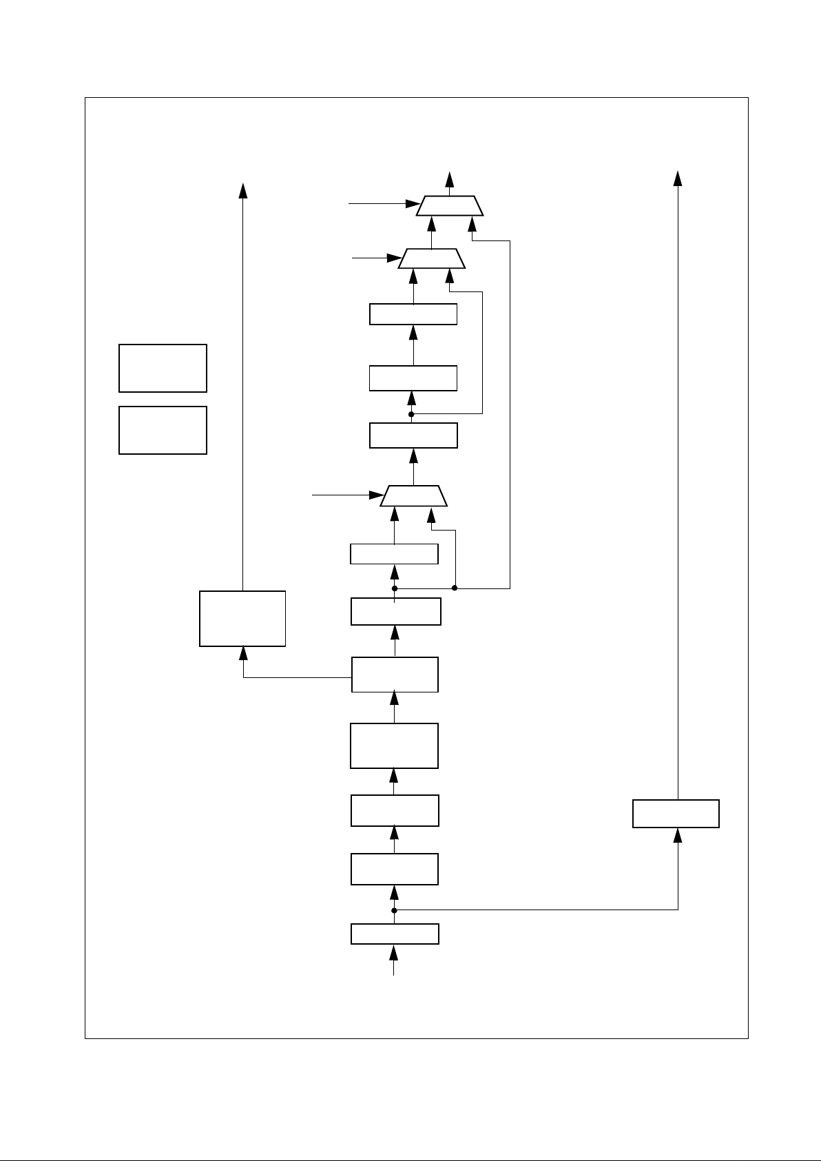
3.9 100BASE-TX TRANSMITTER
The 100BASE-TX transmitter consists of several functional
blocks which convert synchronous 4-bit nibble data, to a
scrambled MLT-3 125 Mb/s serial data stream. Because the
100BASE-TX TP-PMD is integrated, the differential output
pins, TD±, can be directl y routed to the magnetics.
The block diagram in Figure 4 provides an overview of
each functional block within the 100BASE-TX transmit
section.
The Transmitter section consists of the following functional
blocks :
— Code-group Encoder and I njection b lock (byp ass opt ion)
— Scrambler block (bypass option)
— NRZ to NRZI encoder block
— Binary to MLT-3 converter / Common Driver
The bypass option for the functional blocks within the
100BASE-TX transmitter provides flexibility for applications
such as 100 Mb/s repeaters where data conversion is not
always required. The DP83815 implements the 100BASETX transmit state machine diagram as specified in the
IEEE 802.3u Standard, Clause 24
Page 19
3.0 Functional Description
(Continued)
19 www.national.com
Figure 3-6 100BASE-TX Transmit Block Diagram
3.9.1 Code-group Encoding and Injection
The code-group encoder converts 4-bit (4B) nibble data
generated by the MAC into 5-bit (5B) code-groups for
transmission. This conversion is required to allow control
data to be combined with packet data code-groups. Refer
to Table 3-1 for 4B to 5B code-group mapping details.
The code-group encoder substitutes the first 8-bits of the
MAC preamble with a J/K code-group pair (11000 10001)
upon transmission. The code-group encoder continues to
replace subsequent 4B preamble and data nibbles with
corresponding 5B code-groups. At the end of the transmit
packet, upon the de-assertion of Transmit Enable signal
from the MAC, the code-group encoder injects the T/R
code-group pa ir (01 101 001 11) ind icati ng the end of fr ame .
After the T/R code-group pair, the code-group encoder
continuously injects IDLEs into the transmit data stream
until the next transmit packet is detected (re-assertion of
Transmit Enable) .
3.9.2 Scrambler
The scrambler is required to control the radiated emissions
at the media connector and on the twisted pair cable (for
100BASE-TX applications). By scrambling the data, the
total energy launched onto the cable is randomly
distributed over a wide frequency range. Without the
scrambler, energy levels at the PMD and on the cable could
peak beyond FCC limitations at frequencies related to
repeating 5B sequences (i.e., continuous transmission of
IDLEs).
The scrambler is configured as a closed loop linear
feedback shift register (LFSR) with an 11-bit polynomial.
The output of the closed loop LFSR is X-ORd with the
serial NRZ data from the code- group encoder. The result is
a scrambled data stream with sufficient randomization to
decrease radiated emissions at certain frequencies by as
much as 20 dB.
FROM CGM
BP_4B5B
BP_SCR
4B5B CODE-
MUX
5B PARALLEL
SCRAM BLER
MUX
MUX
NRZ TO NRZI
BINARY
100BASE-TX
GROUP ENABLER
TXD(3:0)/
TX_CLK
TX_ER
TO SERIAL
ENCODER
TO MLT-3/
COMMON
DRIVER
LOOPBACK
Page 20
3.0 Functional Description
(Continued)
20 www.national.com
3.9.3 NRZ to NRZI Encoder
After the transmit data stream has been serialized and
scrambled, the data must be NRZI encoded in order to
comply with the TP-PMD standard for 100BASE-TX
transmission over Category-5 un-shielded twisted pair
cable. There is no ability to bypass this block within the
DP83815.
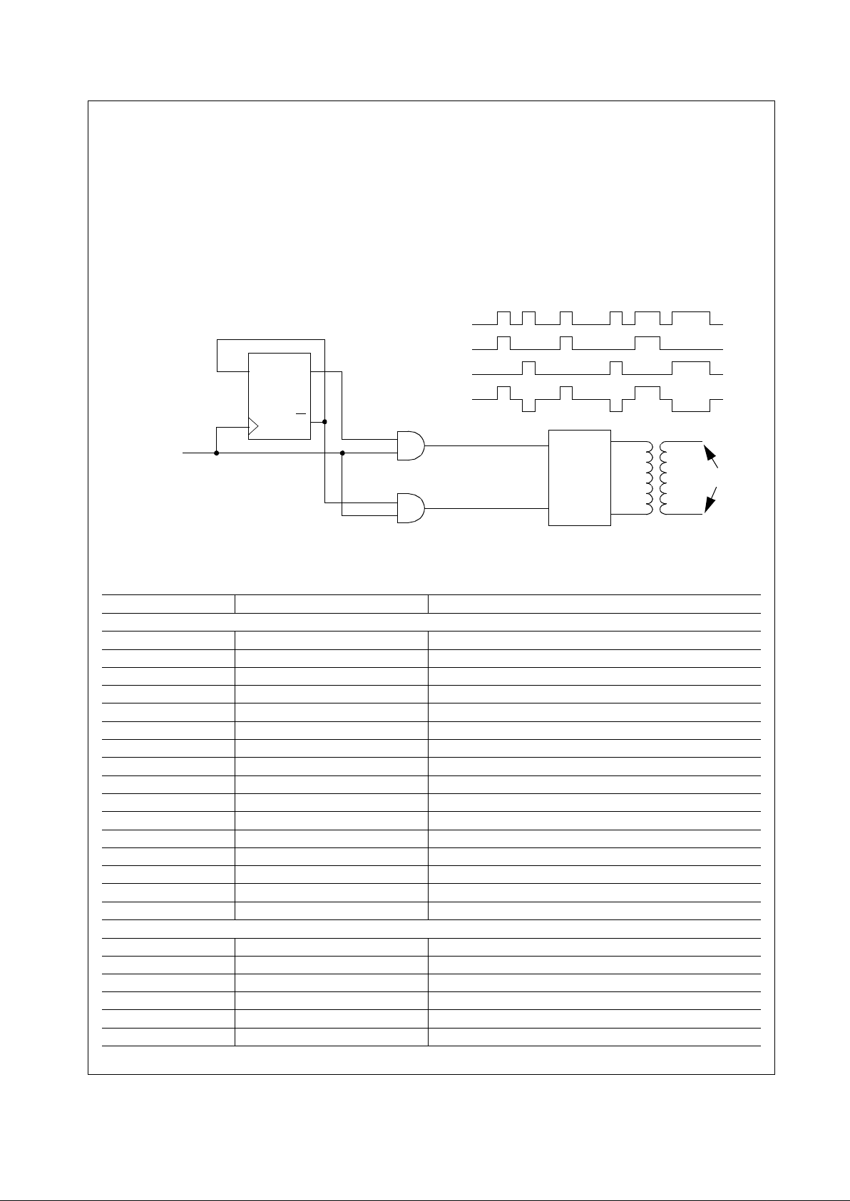
3.9.4 Binary to MLT-3 Convertor / Common Driver
The Binary to MLT-3 conversion is accomplished by
converting the serial binary data stream output from the
NRZI encoder into two binary data streams wit h alt ernately
phased logic one events. These two binary streams are
then fed to t he twi sted pair output driver which con verts the
voltage to current and alternately drives either side of the
transmit t ransf ormer prim ary winding, resul ti ng in a minim al
current (20 mA max) MLT-3 signal. Refer to Figur e3-7
.
Figure 3-7 Binary to MLT-3 conversion
D
Q
Q
binary_in
binary_plus
binary_minus
binary_in
binary_plus
binary_minus
COMMON
DRIVER
MLT-3
differential MLT-3
T able 3-1 4B5B Code-Group Encoding/Decoding
Name PCS 5B Code-group Description/4B Value
DATA CODES
0 11110 0000
1 01001 0001
2 10100 0010
3 10101 0011
4 01010 0100
5 01011 0101
6 01110 0110
7 01111 0111
8 10010 1000
9 10011 1001
A 10110 1010
B 10111 1011
C 11010 1100
D 11011 1101
E 11100 1110
F 11101 1111
IDLE AND CONTROL CODES
H 00100 HALT code-group - Error code
I 11111 Inter-Packet IDLE - 0000
J 11000 First Start of Packet - 0101
K 10001 Second Start of Packet - 0101
T 01101 First End of Packet - 0000
R 00111 Second End of Packet - 0000
Page 21

3.0 Functional Description
(Continued)
21 www.national.com
The 100BASE-TX MLT-3 signal sourced by the TD±
common driver output pins is slew rate controlled. This
should be considered when selecting AC coupling
magnetics to ensure TP-PMD Standard compliant
transit ion times (3 ns < Tr < 5 ns).
The 100BASE-TX transmit TP-PMD function within the
DP83815 is capable of sourcing only MLT-3 encoded data.
Binary output from the TD± outputs is not possible in 100
Mb/s mode.
3.10 100B ASE-TX Receiver
The 100BASE-TX receiver consists of several functional
blocks which convert the scrambled MLT-3 125 Mb/s serial
data stream to synchronous 4-bit nibble data that is
provided to the MAC. Because the 100BASE-TX TP-PMD
is integrated, the differential input pins, RD±, can be
directly routed from the AC coup li ng m agnetics.
See Figure 3-8 for a block diagram of the 100BASE-TX
receive function. This provides an overview of each
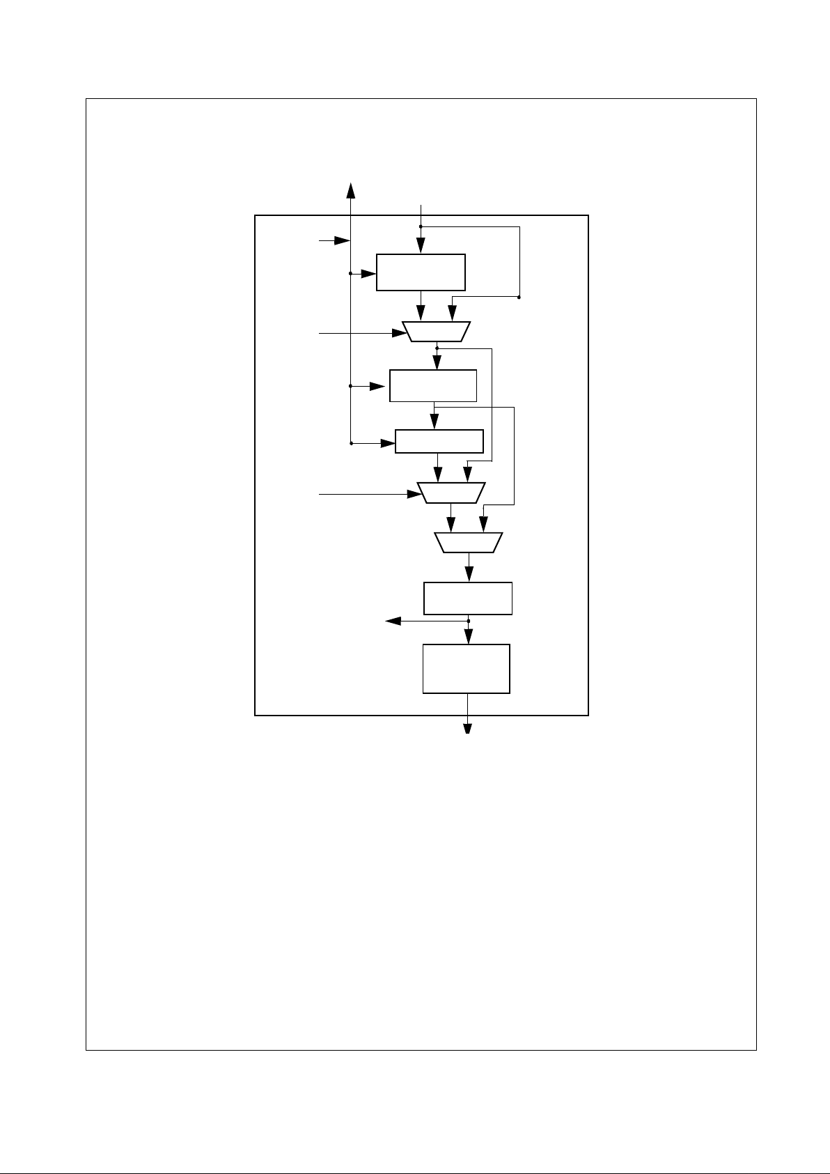
functional block within the 100BASE-TX receiv e section.
The Receive section consists of the following functional
blocks:
—ADC
— Input and BLW Compensation
— Signal Detect
— Digital Adaptive Equalizat ion
— MLT-3 to Binary Decoder
— Clock Recovery Module
— NRZI to NRZ Decoder
— Serial to Par a lle l
— De-scrambler (bypass option)
— Code Group Alignment
— 4B/5B Decoder (bypass option)
— Link Integrity Monitor
— Bad SSD Detection
The bypass option for the functional blocks within the
100BASE-TX receiver provides flexibility for applications
such as 100 Mb/s repeaters where data conversion is not
always required.
3.10.1 Input and Base Line Wander Compensation
Unlike the DP83223V Twister, the DP83815 requires no
external attenuation circuitry at its receive inputs, RD+/−. It
accepts TP-PMD compliant waveforms directly, requiring
only a 100Ω termination plus a simple 1:1 transformer.
The DP83815 is completely ANSI TP-PMD compliant and
includes Base Line Wander (BLW) compensation. The
BLW compensation block can successfully recover the TPPMD defined “killer” pattern and pass it to the digital
adaptive equalization b lock.
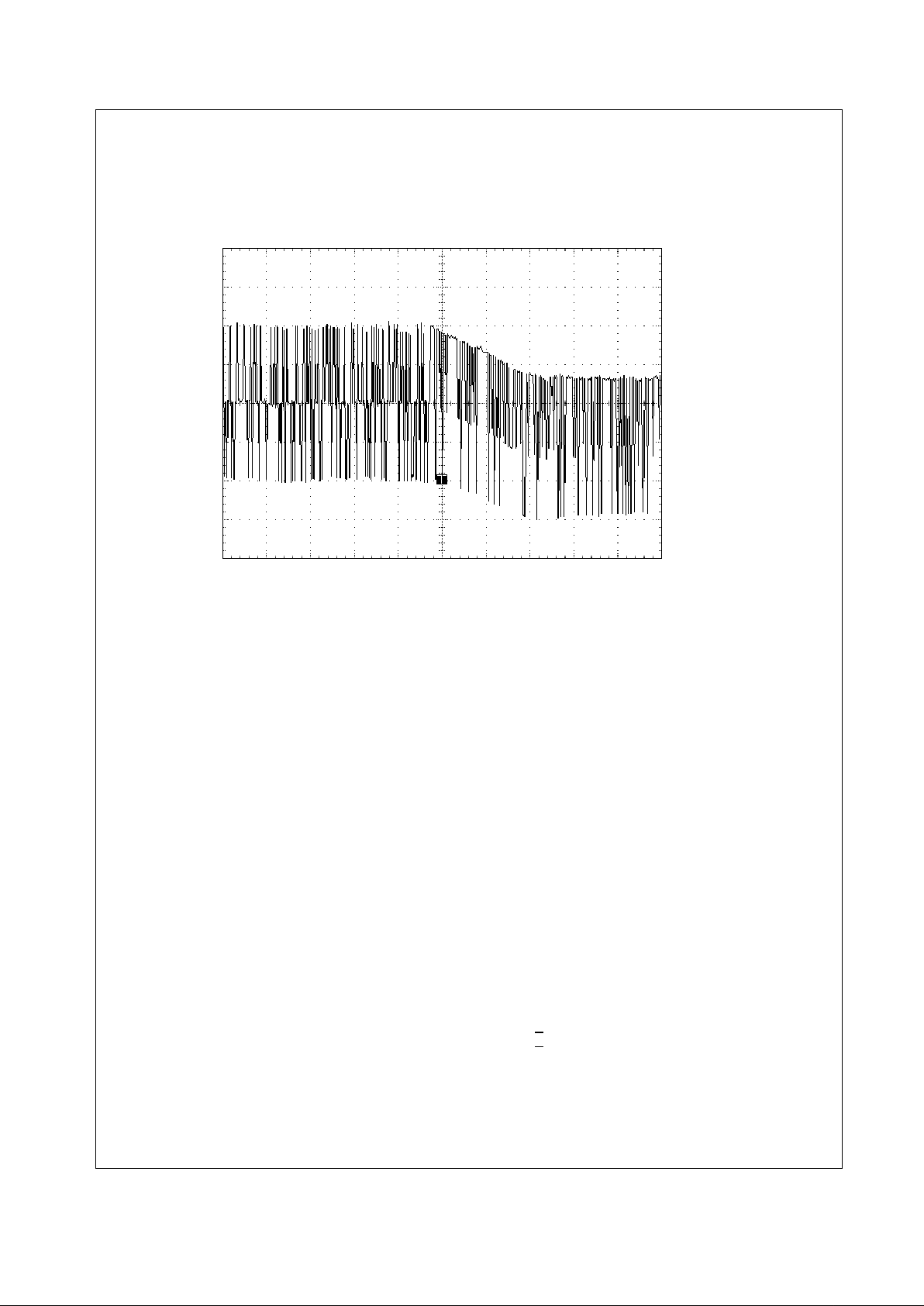
BLW can generally be defined as the change in the
average DC content, over time, of an AC coupled digital
transmission over a given transmission medium. (i.e.
copper wire).
BLW results from the interaction between the low
frequency components of a transmitted bit stream and the
frequency response of the AC coupling component(s)
within the transmission system. If the low frequency
content of the digital bit stream goes below the low
frequency pole of the AC coupling transformers then the
droop characteristics of the transformers will dominate
result ing in p ot e nt ially seri ous B LW.
The digital oscilloscope plot provided in Figure3-9
illustrates the severity of the BLW event that can
theoretically be generated during 100BASE-TX packet
transmission. This event consists of approximately 800 mV
of DC offset for a period of 120 us. Left uncompensated,
events such as this can cause packet loss.
3.10.2 Signal Detect
The signal detect function of the DP83815 is incorporated
to meet the specifi cations mandated by the ANSI FDDI TPPMD Standard as well as the IEEE 802.3 100BASE-TX
Standard for both voltage thresholds and timing
parameters.
Note that the reception of normal 10BASE-T link pulses
and fast link pulses per IEEE 802.3u Auto-Negotiation by
the 100BASE-TX receiver do not cause the DP83815 to
assert signal detect.
3.10.3 Digital Adaptive Equalization
INVALID CODES
V 00000
V 00001
V 00010
V 00011
V 00101
V 00110
V 01000
V 01100
V 10000
V 11001
T able 3-1 4B5B Code-Group Encoding/Decoding
Name PCS 5B Code-group Description/4B Value
Page 22
3.0 Functional Description
(Continued)
22 www.national.com
Figure 3-8 100 M/bs Receive Block Diagram
BP_4B5B
BP_SCR
BP_RX
CLOCK
MUX
MUX
4B/5B DECODER
SERIAL TO
CODE GROUP
MUX
DESCRAMBLER
NRZI TO NRZ
MLT-3 TO BINARY
DIGITAL
CLOCK
LINK INTEGRITY
RX_DATA VALID
AGC
INPUT BLW
ADC
SIGNAL
COMPENSATION
ADAPTIVE
EQUALIZATION
DECODER
DECODER
ALIGNMENT
RECOVERY
MODULE
PARALLEL
MONITOR
SSD DETECT
RX_CLK
SD
RXD(3:0)/RX_ER
RD +/-
DETECT
Page 23
3.0 Functional Description
(Continued)
23 www.national.com
When transmitting data at high speeds over copper twisted
pair cable, frequency dependent attenuation becomes a
concern. In high-speed twisted pair signalling, the
frequency content of the t ransmitted signal can v ary greatly
during normal operation based primarily on the
randomness of the scrambled data stream. This variation in
signal attenuation caused by frequency variations must be
compensated for to ensure the i ntegrity of the transmission.
In order to ensure quality transmission when employing
MLT-3 encoding, the compensation must be able to adapt
to various cable lengths and cable types depending on the
installed environment. The selection of long cable lengths
for a given implementation, requires significant
compensation which will over-compensate for shorter, less
attenuating lengths. Conversely, the selection of short or
intermediate cable lengths requiring less compensation will
cause serious under-compensation for longer length
cables. Therefore, the compensation or equalization must
be adaptive to ensure proper conditioning of the received
signal independent of the cable length.
The DP88315 utilizes a extremely robust equalization
scheme referred to herein as ‘Digital Adaptive
Equalization’. Traditional designs use a pseudo adaptive
equalization scheme that determines the approximate
cable length by monitoring signal attenuation at certain
frequencies. This attenuation value was compared to the
internal receive input reference voltage. This comparison
would indicate the amount of equalization to use. Although
this scheme is used successfully on the DP83223V twister,
it is sensitive to transformer mismatch, resistor variation
and process induced offset. The DP83223V also required
an external a ttenuation network to help match the incoming
signal amplitude to t he internal refer ence.
The Digital Equalizer removes ISI (Inter Symbol
Interference) from the receive data stream by continuously
adapting to provide a filter with the inverse frequency
response of the channel. When used in conjunction with a
gain stage, this enables the receive 'eye pattern' to be
opened sufficiently to allow very reliable data recovery.
Traditionally 'adaptive' equalizers selected 1 of N filters in
an attempt to match the cables characteristics. This
approach will typically leave holes at certain cable lengths,
where the performance of the equalizer is not optimized.
The DP83815 equalizer is t ruly adaptive.
The curves given in Figure 3-10 illustrate attenuation at
certain frequencies for given cable lengths. This is derived
from the worst case frequency vs. attenuation figures as
specified in the EIA/TIA Bulletin TSB-36. These curves
indicate the significant variations in signal attenuation that
must be compensated for by the receive adaptive
equalization circuit.
Figure 3-11 represents a scrambled IDLE transmitted over
zero meters of cable as measured at the AII (Active Input
Interface) of the receiver. Figure3-12 and Figure3-13
represent th e signal deg radation over 50 and 100 meters of
category V
cable respectively, also measured at the AII.
These plots show the extreme degradation of signal
integrity and indicate the requirement for a robust adaptive
equalizer.
Figure 3-9 100BASE-TX BLW Event Diagram
Page 24

2ns/div
Page 25

3.0 Functional Description
(Continued)
25 www.national.com
3.10.6 Clock Recovery Module
The Clock Recovery Module (CRM) accepts 125 Mb/s
MLT3 data from the equalizer . The DPLL lock s onto the 125
Mb/s data stream and extracts a 125 MHz recovered clock.
The extracted and synchronized clock and data are used
as required by the synchronous receive operations as
generally depicted in Figure 3-8.
The CRM is implemented using an advanced all digital
Phase Locked Loop (PLL) architecture that replaces
sensitive analog circuitry. Using digital PLL circuitry allows
the DP83815 to be manufactured and specified to tighter
tolerances.
3.10.7 NRZI to NRZ
In a typical application, the NRZI to NRZ decoder is
required in order to present NRZ for matted data to the descrambler (or to the code-group alignment block, if the descrambler is bypassed, or directly to the PCS, if the
receiver is bypass ed).
3.10.8 Serial to Parallel
The 100BASE-TX receiver includes a Serial to Parallel
converter which supplies 5-bit wide data symbols to the
PCS Rx state machine.
3.10.9 De-scrambler
A serial de-scrambler is used to de-scramble the received
NRZ data. The de-scrambler has to generate an identical
data scrambling sequence (N) in order to recover the
original unscrambled data (UD) from the scrambled data
(SD) as represent ed in the equations:
Synchronization of the de-scrambler to the original
scrambling sequence (N) is achieved based on the
knowledge that the incoming scrambled data stream
consists of scrambled IDLE data. After the de-scrambler
has recognized 12 consecutive IDLE code-groups, where
an unscrambled IDLE code-group in 5B NRZ is equal to
five consecutive ones (11111), it will synchronize to the
receive data stream and generate unscrambled data in the
form of unaligned 5B code-groups.
In order to maintain synchronization, the de-scrambler
must continuously monitor the validity of the unscrambled
data that it generates. To ensure this, a line state monitor
and a hold timer are used to constantly monitor the
synchronization status. Upon synchronization of the descrambler the hold timer starts a 722 µs countdown. Upon
detection of sufficient IDLE code-groups (58 bit times)
within the 722 µs period, the hold timer will reset and begin
a new countdown. This monitoring operation will continue
indefinitely given a properly operating network connection
with good signal integrity. If the line state monitor does not
recognize sufficient unscrambled IDLE code-groups within
the 722 µs period, the entir e de-scrambler will be for ced out
of the current state of synchronization and reset in order to
re-acquire synchronization.
3.10.10 Code-group Alignment
The code-group alignment module operates on unaligned
5-bit data from the de-scrambler (or, if the de-scrambler is
bypassed, directly from the NRZI/NRZ decoder) and
converts it into 5B code-group data (5 bits). Code-group
alignment occurs after the J/K code-group pair is detected.
Once the J/K code-group pair (11000 10001) is detected,
subsequent data is aligned on a fixed boundary.
3.10.11 4B/5B Decoder
The code-group decoder functions as a look up table that
translates incoming 5B code-groups into 4B nibbles. The
code-group decoder first detects the J/K code-group pair
preceded by IDLE code-groups and replaces the J/K with
MAC preamble. Specifically, the J/K 10-bit code-group pair
is replaced by the nibble pair (0101 0101). All subsequent
5B code-groups are converted to the corresponding 4B
nibbles for the duration of the entire packet. This
conversion ceases upon the detection of the T/R codegroup pair denoting the End of Stream Delimiter (ESD) or
with the reception of a minimum of two IDLE code-groups.
3.10.12 100BASE-TX Link Integrity Monitor
The 100 Base-TX Link monitor ensures that a valid and
stable link is established before enabling both the Transmit
and Receive PCS la yer.
Signal detect must be valid for 395 µs to allow the link
monitor to ente r t he 'Link Up' state , and enable the t ransmit
and receive fu nctions.
Signal detect can be forced active by setting Bit 1 of the
PCSR.
Signal detect can be optionally ANDed with the descrambler locked indication by setting bit 8 of the PCSR.
When this option is enabled, then De-scrambler 'locked' is
required to e nter the Link Up state, but only Signal det ect is
required to maintain the link in the link Up state.
3.10.13 Bad SSD Detection
A Bad Start of Stream Del imiter (Bad SSD) is any transition
from consecutive idle code-groups to non-idle code-groups
which is not prefixed by the code-group pair J/K.
If this condition is detected, the DP83815 will assert
RX_ER and present RXD[3:0] = 1110 to the MAC for the
cycles that correspond to received 5B code-groups until at
least two IDLE code groups are detected. In addition, the
False Carrier Event Counter will be incremented by one.
Once at least t w o IDLE code group s are detected, the error
is reported to the MAC .
3.11 10BASE-T Transceiver Module
The 10BASE-T Transceiver Module is IEEE 802.3
compliant. It includes the receiver, transmitter, collision,
heartbeat, loopback, jabber, and link integrity functions, as
defined in the standard. An external filter is not required on
the 10BASE-T interface since this is integrated inside the
DP83815. This section focuses on the general 10BASE-T
system level operat ion.
3.11.1 Operational Modes
The DP83815 has two basic 10BASE-T operational
modes:
— Half Duplex mode - functions as a standard IEEE 802.3
10BASE-T transceiver supporting the CSMA/CD
protocol.
— Full Duplex mode - capable of simultaneously
transmitting and receiving without reporting a collisi on.
The DP83815's 10 Mb/s ENDEC is designed to encode
and decode simultaneously.
UD SD N
⊕()=
SD UD N
⊕()=
Page 26
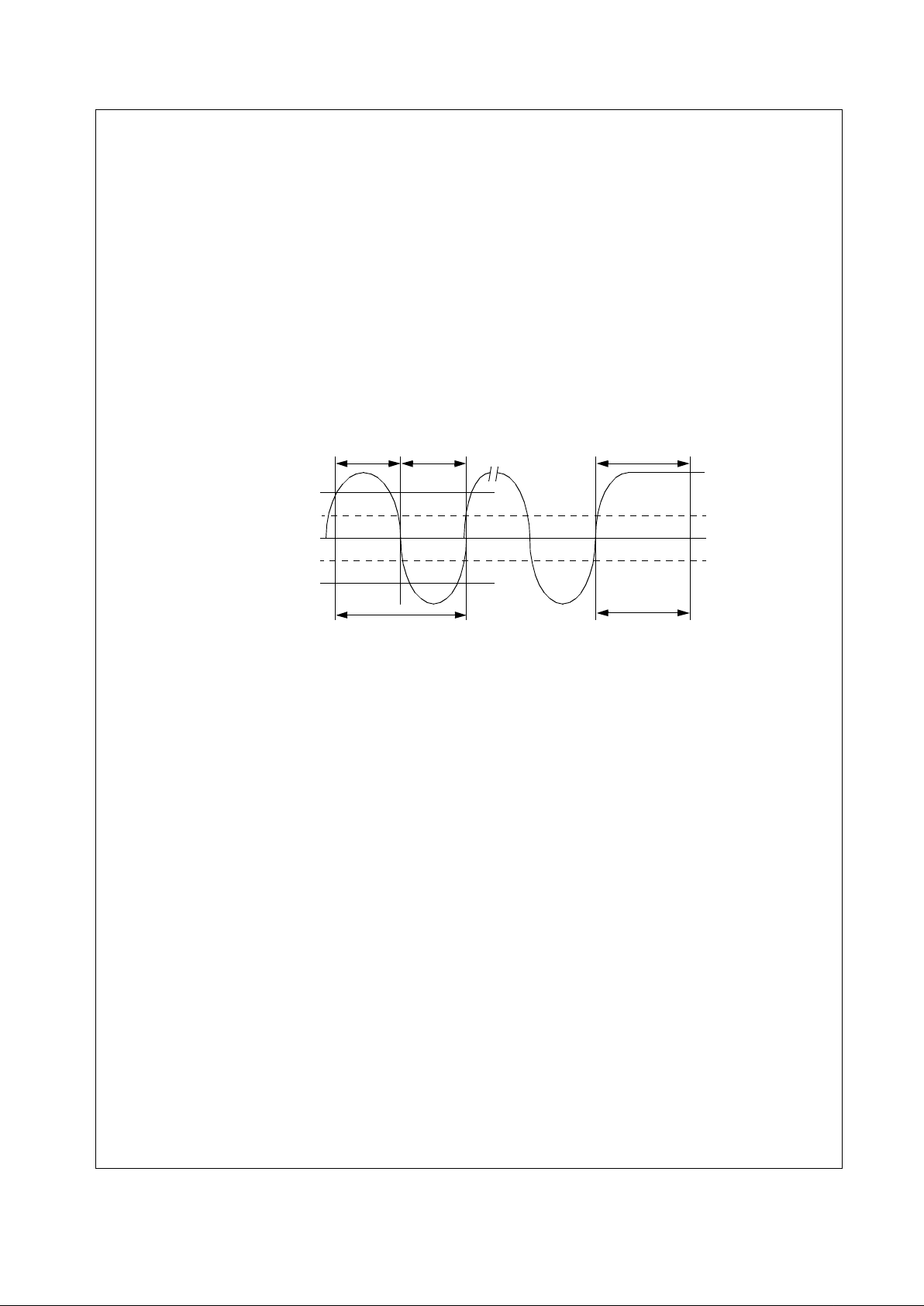
3.0 Functional Description
(Continued)
26 www.national.com
3.11.2 Smart Squelch
The smart squelch is responsible for determining when
valid data is present on the differential receive inputs
(RD±). The DP83815 implements an intelligent receive
squelch to ensure that impulse noise on the receive inputs
will not be mistaken for a valid signal. Smart squelch
operation is independent of the 10BASE-T operational
mode.
The squelch circuitry employs a combination of amplitude
and timing measurements (as specified in the IEEE 802.3
10BASE-T standard) to determine the validity of data on
the twisted pair i nputs (refer to Figure 3-14).
The signal at the start of packet is checked by the smart
squelch and any pulses not exceeding the squelch level
(either positive or negative, depending upon polarity) will
be rejected. Once this first squelch level is overcome
correctly, the opposite squelch level must then be
exceeded within 150 ns. Finally the signal must again
exceed the original squelch level within a 150 ns to ensure
that the input waveform will not be rejected. This checking
procedure results i n the loss of typicall y three pre amb le bits
at the beginning of each packet.
Only after all these conditions have been satisfied will a
control signal be generated to indicate to the remainder of
the circuitry that valid data is present. At this time, the
smart squelch circuitry is reset.
Valid data is considered to be present until the squelch
level has not been generated for a time long er than 150 ns,
indicating the End of Packet. Once good data has been
detected the squelch levels are reduced to minimize the
effect of noise causing premature End of Packet detection.
3.11.3 Collision Detection
When in Half Duplex, a 10BASE-T collision is detected
when the receive and transmit channels are active
simultaneously. Collisions are reported to the MAC.
Collisions are also reported when a jabber condition is
detected.
If the ENDEC is receiving when a collision is detected it is
reported immediately (t hrough the COL signal).
When heartbeat is enabled, approximately 1 µs after the
transmission of each packet, a Signal Quality Error (SQE)
signal of approximat ely 10 bit ti me s is generated to indicate
successful transmission.
The SQE test is inhibited when the physical layer is set in
full duplex mode. SQE can also be inhibited by setting the
HEARTBEAT_DIS bit in the TBTSCR register.
3.11.4 Normal Link Pul se Detection/Generation
The link pulse generator produces pulses as defined in the
IEEE 802.3 10BASE-T standard. Each link pulse is
nominally 100 ns in duration and transmitted every 16 ms
in the absence of transmit data.
Link pulses are used to check the integrity of the
connection with the remote end. If valid link pulses are not
received, the link detector disables the 10BASE-T twisted
pair transmitter, receiver and collision detection functions.
When the link integrity function is disabled
(FORCE_LINK_10 of the 10BTSCR register), good link is
forced and the 10BASE-T transceiver will operate
regardless of the presence of link pulses.
3.11.5 Jabber Function
The jabber function monitors the DP83815's output and
disables the transmitter if it attempts to transmit a packet of
longer than legal size. A jabber timer monitors the
transmitter and disables the transmission if the transmitter
is active for approximately 20-30 ms.
Once disabled by the jabber function, the transmitter stays
disabled for the entire time that the ENDEC module's
internal transmit enable is asserted. This signal has to be
de-asserted for approximately 400-600 ms (the “unjab”
time) before the jabber function re-enables the transmit
outputs.
The Jabber function is only meaningful in 10BASE-T mode.
3.11.6 Automatic Link Polarity Detection
The DP83815's 10BASE-T transceiver module
incorporates an automatic link polarity detection circuit.
When seven consecutive link pulses or three consecutive
receive packets with inverted End-of-Packet pulses are
received, bad polarity is reported.
A polarity reversal can be caused by a wiring error at eit her
end of the cable, usually at the Main Distribution Frame
(MDF) or patch panel in the wiring cl oset.
The bad polarity condition is latched. The DP83815's
10BASE-T transceiver module corrects for this error
internally and will continue to decode received data
Figure 3-14 10BASE-T Twisted Pair Smart Squelch Operation
end of packet
start of packet
V
SQ-(reduced)
V
SQ-
V
SQ+(reduced)
V
SQ+
<150 ns
<150 ns
>150 ns
Page 27

27 www.national.com
correctly. This eliminates the need to correct the wiring
error immediat ely.
3.11.7 10BASE-T Internal Loopback
When the LOOPBACK bit in the BMCR register is set,
10BASE-T transmit data is looped back in the ENDEC to
the receive channel. The transmit drivers and receive input
circuitry are disabled in transceiver loopback mode,
isolating the t ransceiv er from the network.
Loopback is used for diagnostic testing of the data path
through the transceiver without transmitting on the network
or being interrupted by receive traffic. This loopback
function causes the data to loopback just prior to the
10BASE-T output driver buffers such that the entire
transceiver path is tested.
3.11.8 Transmit and Receive Filtering
External 10BASE-T filters are not required when using the
DP83815, as the required signal conditioning is integrated
into the device.
Only isolation/step-up transformers and impedance
matching resistors are required for the 10BASE-T transmit
and receive interface. The internal transmit filtering
ensures that all the harmonics in the transmit signal are
attenuated by at least 30 dB.
3.11.9 Transmitter
The encoder begins operation when the transmit enable
input to the physical layer is asserted and converts NRZ
data to pre-emphasized Manchester data for the
transceiver. For the duration of assertion, the serialized
transmit data is encoded for the transmit-driver pair (TD±).
The last transition is always positive; it occurs at the center
of the bit cell if the last bit is a one, or at the end of the bit
cell if the last bit is a zero.
3.11.10 Receiver
The decoder consist s of a di fferential receiver and a PLL to
separate a Manchester encoded data stream into internal
clock signals and data. The differential input must be
externally terminated with a differential 100Ω termination
network to accommodate UTP cab le.
The decoder detects the end of a frame when no more midbit transitions are detected.
3.11.11 Far End Fault Indication
Auto-Negotiation provides a mechanism for transferring
information from the Local Station to the Li nk Partner that a
remote fault has occurred for 100BASE-TX.
A remote fault is an error in the link that one station can
detect while the other cannot. An example of this is a
disconnected f iber at a station’s transm itter. This station will
be receiving valid data and detect that the link is good via
the Link Integrity Monitor, but will not be able to detect that
its transmission is not propagati ng to t he other station.
If three or more FEFI IDLE patterns are detected by the
DP83815, then bit 4 of the Basic Mode Status register is
set to one until read by management, additionally bit 7 of
the PHY Status register is also set.
The first F EFI IDLE pattern may contain m ore than 84 ones
as the pattern may have started during a normal IDLE
transmission which is actually quite likely to occur.
However, since FEFI is a repeating pattern, this will not
cause a problem with the FEFI function. It should be noted
that receipt of the FEFI IDLE pattern will not cause a
Carrier Sense error to be reported.
If the FEFI function has been disabled via FEFI_EN (bit 3)
of the PCSR Configuration register, then the DP83815 will
not send the FEFI IDLE pattern.
Page 28

28 www.national.com
4.0 Register Set
4.1 Configuration Registers
The DP83815 implements a PCI version 2.2 configuration register space. This allows a PCI BIOS to "soft" configure the
DP83815. Software Reset has no effect on configuration regi sters. Hardware Reset returns all configuration registers to
their hardware reset state. For all unused registers, writes are ignored, and reads return 0.
Table 4-1 Configuration Register Map
4.1.1 Configuration Identification Register
This register identifies the DP83815 Controller to PCI system soft ware.
Offset Tag Description Access
00h CFGID Configuration Identification Register RO
04h CFGCS Configuration Command and Status Register R/W
08h CFGRID Configuration Revision ID Register RO
0Ch CFGLAT Configuration Latency Timer Register RO
10h CFGIOA Configuration IO Base Address Register R/W
14h CFGMA Configuration Memory Address Register R/W
18h-28h Reserved (reads return zero)
2Ch CFGSID Configuration Subsystem Identification Register RO
30h CFGROM Boot ROM configuration register R/W
34h CAPPTR Capabiliti es Pointer Register RO
38h Reserv ed (reads return zero)
3Ch CFGINT Configuration Interrupt Select Register R/W
40h PMCAP Power Ma nagement Capabilities Register RO
44h PMCSR Power Management Control and Status Register R/W
48-FFh Reserve d (reads return zero)
Tag:
CFGID
Size:
32 bits
Hard Reset:
0020100Bh
Offset:
00h
Access:
Read Only
Soft Reset:
Unchanged
Bit Bit Name Descriptio n
31-16 DEVID
Device ID
This field is read-only and is set to the device ID assigned by NSC to the DP83 815, whic h is 0020h.
15-0 VENID
Vendor ID
This field is read-only and is set to a value of 100Bh which is National Semiconductor's PCI Vendor ID.
Page 29

29 www.national.com
4.0 Register Set
(Continued)
4.1.2 Configurati on Command and Status Register
The CFGCS register has tw o parts. The upper 16-bits (31-16) are devoted to device status. A status bit i s reset whenever
the register is written , and the corre sponding bit locat ion is a 1.
The lower 16-bi ts (15- 0) are de vot ed to command and are
used to configure and control the device.
Tag:
CFGCS
Size:
32 bits
Hard Reset:
02900000h
Offset:
04h
Access:
Read Write
Soft Reset:
Unchanged
Bit Bit Name Description
31 DPERR
Detected Parity Error
Refer to th e description in the PCI V2.2 specification.
30 SSERR
Signaled SERR
Refer to th e description in the PCI V2.2 specification.
29 RMABT
Received Master Abort
Refer to th e description in the PCI V2.2 specification.
28 RTABT
Received Target Abort
Refer to th e description in the PCI V2.2 specification.
27 ST ABT
Sent Target Abort
Refer to th e description in the PCI V2.2 specification.
26-25 DSTIM
DEVSELN Timing
This field will always be set to 01 indicating that DP83815 supports “medium” DEVSELN timing.
24 DPD
Data Parity Detected
Refer to th e description in the PCI V2.2 specification.
23 FBB
Fast Back-to-Back Capable
DP83815 will s e t this bit to 1.
22-21
unused
(reads return 0)
20 NCPEN
New Capabilities Enable
When set, this bit indicates that the Capabilities Pointer contains a valid value and new capabilities such
as power management are supported. When clear, new capabilities (CAPPTR, PMCAP, PMCS) are
disab l ed. Th e v a lu e i n th is r egist e r wil l e ith er be lo aded fr o m the E EPR O M o r , i f th e E EPR OM i s d is ab l e d,
from a strap option at reset.
19-16
Unused
(reads return 0)
15-10
Unused
(reads return 0)
9 FBBEN
Fast Back-to-Back Enable
Set to 1 by the P CI BIOS to enable the DP83815 to do Fa st Back-to-Back tr ansfers (FBB transfers as a
master is not implemented in the c urrent revision).
8 SERREN
SERRN Enable
When SERREN and PERRSP are set, DP83815 will generate SERRN during target cycles when an
address parity error is detected from the system. Also, when SERREN and PERRSP are set and
CFG:PESEL is reset, master cycles detecting data parity errors will generate SERRN.
7
Unused
(reads return 0)
Page 30

30 www.national.com
4.0 Register Set
(Continued)
4.1.3 Configuration Revision ID Register
This register stores the silicon revision number, revision number of software interface specification and lets the
configura tion software know that it is an Ethernet controll er in the class of netwo rk cont rollers.
.
Bit Bit Name Description
6 PERRSP
Parity Error Response
When set, DP83815 will assert PERRN on the detection of a data parity error when acting as the target,
and will sample PERRN when acting as the initiator. Also, setting PERRSP allows SERREN to enable
the assertion of SERRN. When reset, all address and data parity errors are ignored and neither SERRN
nor PERRN are asserted.
5-3
Unused
(reads return 0)
2 BMEN
Bus Mast er Enable
When se t, DP83815 is allowed t o act as a PCI bus master. When reset, DP83815 is prohibited from
acting as a PCI bus master.
1 MSEN
Memory Space Address
When set, DP83815 respon ds to memory space accesses. When reset, DP83815 ignor es memory
space accesses.
0 I/OSEN
I/O Space A ccess
When se t, DP83815 responds to I/O space accesses. When re set, DP83815 ignores I/O space
accesses.
Tag:
CFGRID
Size:
32 bits
Hard Reset:
02000000h
Offset:
08h
Access:
Read Only
Soft Reset:
Unchanged
Bit Bit Name Description
31-24 BASECL
Base Class
Retu r ns 02h whi ch specifie s a netw or k control ler.
23-16 SUBCL
Sub Class
Returns 00 h w hi ch spe ci fie s an Ethernet cont ro ller.
15-8 PROGIF
Programming IF
Returns 00h which specifies the first release of the DP83815 Software Interface Specification.
7-0 REVID
Silicon Revision
Returns 00h which specifies the silicon revision.
Page 31

31 www.national.com
4.0 Register Set
(Continued)
4.1.4 Configuration Latency Timer Register
This register gives status and controls such miscel laneous functions as BI ST, Latency timer and Cache line size.
.
DP83815 Bus Master Operations:
Independent of cac he line size, th e DP83815 will use the following PCI commands for bus mastered transfers:
0110 - Mem Read for all read cycl es,
0111 - Mem Write for all write cycles.
4.1.5 Configuration I/O Base Address Register
This register specifies the Base I/O address which is required to build an address map during configuration. It also
specifies the number of bytes required as well as an indication that it can be mapped into I/O space.
.
Tag:
CFGLAT
Size:
32 bits
Hard Reset:
00000000h
Offset:
0Ch
Access:
Read Write
Soft Reset:
Unchanged
Bit Bit Name Description
31 BISTCAP
BIST Capable
Reads will always return 0.
30 BISTEN
BIST Enable
Reads will return a 0, w rites are ignored .
29-16
Reserved
Reads will return a 0, w rites are ignored .
15-8 LAT
Latency Timer
Set by software to the number of PCI clocks that DP83815 may hold the PCI bus.
7-0 CLS
Cache Line Size
Ignored by DP83815.
Tag:
CFGIOA
Size:
32 bits
Hard Reset:
00000001h
Offset:
10h
Access:
Read Write
Soft Reset:
Unchanged
Bit Bit Name Description
31-8 IOBASE
Base I/O Address
This is set by software to the base I/O address for the Operati onal Regi ster Map.
7-2 IOSIZE
Size indication
Read back as 0. This allows the PCI b ridge to determine that the DP83815 requires 256 bytes o f I/O
space .
1
Unused
(reads return 0).
0 IOIND
I/O Space Indicator
Set to 1 by DP83815 to indicate t hat DP83815 is ca pable of being mapped into I/O space. Read O nly.
Page 32

32 www.national.com
4.0 Register Set
(Continued)
4.1.6 Configuration Memory Address Register
This register specifies the Base Memory address which is required to build an address map during configuration. It also
specifies the number of bytes required as well as an indication that it can be mapped into memory space.
.
4.1.7 Configuration Subsystem Identification Register
The CFGSID allows system software to distinguish between different subsystems based on the same PCI silicon. The
values in this register can be loaded from the EEPROM if configuration is enabled.
.
Tag:
CFGMA
Size:
32 bits
Hard Reset:
00000000h
Offset:
14h
Access:
Read Write
Soft Reset:
unchanged
Bit Bit Name Description
31-12 MEMBASE
Memory Base Address
This i s set by s oftware to the base addr ess f or the Operational Register Map.
11-4 MEMSIZE
Memory Size
These bits return 0, which indicates that the DP83815 requires 4096 bytes of Memory Space (the
minim um recommended all ocation).
3 MEMPF
Prefetchable
Set to 0 by DP83815. Read Only.
2-1 MEMLOC
Location Selection
Set to 00 by DP83815. This indicates that the base register is 32-bits wide and can be placed anywhere
in the 32-bit me mory space. Read Only.
0 MEMIND
Memory Space Indicator
Set to 0 by DP83815 to indicate that DP8381 5 is capable of being mapped into memory space. Read
Only.
Tag:
CFGSID
Size:
32 bits
Hard Reset:
00000000h
Offset:
2Ch
Access:
Read Only
Soft Reset:
unchanged
Bit Bit Name Description
31-16 SDEVID
Subsystem Device ID
Set to 0 by DP83815.
15-0 SVENID
Subsystem Vendor ID
Set to 0 by DP83815
Page 33

33 www.national.com
4.0 Register Set
(Continued)
4.1.8 Boot ROM Configuration Register
4.1.9 Capabiliti es Pointer Register
This register stores the capabilities linked list offset into the PCI configuration space.
Tag:
CFGROM
Size:
32 bits
Hard Reset:
00000000h
Offset:
30h
Access:
Read Write
Soft Reset:
unchanged
Bit Bit Name Description
31-16 ROMBASE
ROM Base Address
Set to the base address for the boot ROM.
15-11 ROMSIZE
ROM Size
Set to 0 indicating a requirement for 64K bytes of Boot ROM space. Read only.
10-1
unused
(reads return 0)
0 ROMEN
ROM Enable
This is used by the PCI BIOS to enable accesses to boot ROM. This allows the DP83815 to share the
address decode logic between the boot ROM and itself. The BIOS will copy the contents of the boot ROM
to system RAM before executing it. Set to 1 enables the address decode for boot ROM disabling access
to operational target registers.
Tag:
CAPPTR
Size:
32 bits
Hard Reset:
00000040h
Offset:
34h
Access:
Read Only
Soft Reset:
unchanged
Bit Bit Name Description
31-8
unused
(reads return 0)
7-0 CLOFS
Capabilities List Offset
Offset into PCI configuration space for the location of the first item in the Capabilities Linked List, set to
40h to point to the PMCAP register.
Page 34

34 www.national.com
4.0 Register Set
(Continued)
4.1.10 Configuration Interrupt Select Register
This register stores the interrupt line number as identified by the POST software that is connected to the interrupt
controller as well as DP83815 desired settings for maximum latency and minimum grant. Max latency and Min latency
can be loaded from the EEPROM.
4.1.11 Power Management Capabilities Register
This register provides information on the capabilities of the functions related to power management. This register also
contains a pointer to the next item in the capabilities list and the capabilit y ID for Power Management. This register is only
visibl e if CF GCS[4] is set.
Tag:
CFGINT
Size:
32 bits
Hard Reset:
340b0100h
Offset:
3Ch
Access:
Read Write
Soft Reset:
unchanged
Bit Bit Name Description
31-24 MXLAT
Maximum Latency
The DP 83815 desired setting f or Max Latency. The DP83815 will initialize this field to 52d (13 usec). The
value in this register can be loaded from the EEPROM.
23-16 MNGNT
Minimum Grant
The DP83815 desired setting for Minimum Grant. The DP83815 will initialize this field to 11d (2.75 usec).
The v alue in this register can be loaded from the EEPROM .
15-8 IPIN
Interrupt Pin
Read Only, always return 0000 0001 (INTA)
7-0 ILINE
Interrupt Line
Set to which line on the interrupt controller that the DP83815's interrupt pin is connected to.
Tag:
PMCAP
Size:
32 bits
Hard Reset:
FF820001
Offset:
40h
Access:
Read Only
Soft Reset:
unchanged
Bit Bit Name Description
31-27 PMES
PME Support
This 5 bit field indicates the power states in which DP83815 may assert PMEN. A 1 indicates PMEN
is enabled for that state, a 0 indicates PMEN is inhibited in that s tate.
XXXX1 - PMEN can be asserted from state D0
XXX1X - PMEN can be asserted from state D1
XX1XX - PMEN can be asserted from state D2
X1XXX - PMEN can be asserted from state D3hot
1XXXX - PMEN can be asserted from state D3cold
The DP 83815 w i ll on ly r ep ort PM E sup po rt f or D3 col d if auxi l ia ry po w er i s d et ec t ed on th e 3 VAUX pin ,
in addi tion this value can be loaded from the EEPROM when in the D3cold state.
26 D2S
D2 Support
This bit is set to a 1 when the DP83815 supports the D2 state.
25 D1S
D1 Support
This bit is set to a 1 when the DP83815 supports the D1 state.
Page 35

35 www.national.com
4.0 Register Set
(Continued)
4.1.12 Power Management Control and Status Register
This register contains PM control and st atus information.
Bit Bit Name Description
24-22 AUX_CURRENT
Aux_Current
This 3 bit field reports the 3.3Vaux auxiliary current requirements for the PCI function.
If PMEN generation from D3cold is not supported by the function(PMCAP[31]), this field returns a
value of "000b" when read.
Bit 3.3V aux
24 23 22 (bits) M
ax. Current Required
1 1 0 320 mA
0 0 0 0 (self powered)
21 DSI
Device Specific Initialization
This bi t is set to 1 to indicate to the system that initialization of the DP 83815 device is required
(beyond the standard PCI configuration header) before the generic class device driver is able to use
it. A 1 indicate s that DP83815 requires a DSI sequence fol lowin g transition to the D0 uninitiali zed
state. This bit can be loaded from the EEPROM.
20
Reserved
(reads return 0)
19 PMEC
PME Clock
Returns 0 to indicate PCI clock not needed for PMEN.
18-16 PMV
Power Management Version
This bit field indicates compliance to a specific PM specification rev level. Currently set to 010b.
15-8 NLIPTR
Next List Item Pointer
Offset into PCI configuration space for the location of the next item in the Capabilities Linked List.
Retur n s 00 h as n o oth er ca pa bi lities are offere d.
7-0 CAPID
Capability ID
Always returns 01h for Power Manageme nt ID.
Tag:
PMCSR
Size:
32 bits
Hard Reset:
00000000h
Offset:
44h
Access:
Read Write
Soft Reset:
unchanged
Bit Bit Name Description
31-24
Reserved
(reads return 0)
23-16 BSE
Bridge Support Extensions
unused (reads return 0)
15 PMESTS
PME Status
Sticky bit which rep resents the state of the PME logic , regar dless of the state of the PM EEN bit.
14-9 DSCALE
Data Scale
Reserved (reads return 0)
8 PMEEN
PME Enable
When set to 1, this bit enables the assertion of the PME functio n on the PMEN pin. When 0, the PMEN
pin is forced to be inactive. This value can be loaded from the EEPROM.
7-2
Unused
(reads return 0)
1-0 PSTATE
Power State
This 2 b it field is used to determine the current power state of DP83815, and to set a new power state.
00 - D0 10 - D2
01 - D1 11 - D3hot
Page 36

36 www.national.com
4.0 Register Set
(Continued)
4.2 Operational Re gisters
The DP83815 provides the following set of operational registers mapped into PCI memory space or I/O space. Writes to
reserved register locations are ignored. Reads to reserved register locations return undefined values.
T able 4-2 Operational Register Map
Offset Tag Description Access
MAC/BIU Registers
00h CR Command Register R/W
04h CFG Configuration Register R/W
08h MEAR E EP ROM Access Register R/W
0Ch PTSCR PCI Test Control Register R/W
10h ISR Interrupt Status Register RO
14h IMR Interrupt Mask Register R/W
18h IER Interrupt Enable Register R/W
1Ch Reserved
20h TXDP Transmit Descriptor Pointer Register R/W
24h TXCFG Transmit Configuration Register R/W
28-2Ch Reserved
30h RXDP Receive Descriptor Pointer Register R/W
34h RXCFG Rec ei ve Configur ation Registe r R/W
38 Reserve d
3Ch CCSR CLKRUN Control/Status Register R/W
40h WCSR Wake on LAN Control/Status Register R/W
44h PCR Pause Control/Sta tus Register R/W
48h RFCR Receive Filter/Match Control Register R/W
4Ch RFDR Receive Filter/Match Data Register R/W
50h BRAR Boot ROM Address R/W
54h BRDR Boot ROM Data R/W
58h SRR Silicon Revision Register RO
5Ch MIBC Management Information Base Control Register R/W
60-78h MIB Management Information Base Data Registers RO
7Ch Reserved
Internal Phy Regi sters
80h BMCR Basic Mode Control Register R/W
84h BMSR Basic Mode Status Register RO
88h PHYIDR1 PHY Identifier Register #1 RO
8Ch PHYIDR2 PHY Identifier Register #2 RO
90h ANAR Auto-Negotiation Advertisement Register R/W
94h ANLPAR Auto-Negotiation Link Partner Ability Register R/W
98h ANER Auto-Negotiation Expansion Register R/W
9Ch ANNPTR Auto-Negotiation Next Page TX R/W
A0-BCh Reserved Reserved
C0h PHYSTS PHY Status Register RO
C4h MICR MII Interrupt Control Register RW
C8h MISR MII Interrupt Status Register RW
CCh Res erved Reserve d
D0h FCSCR False Carrier Sense Counter Register R/W
D4h RECR Receive Error Counter Register R/W
D8h PCSR 100 Mb/s PCS Configuration and Status Register R/W
DCh-E0h Reserved Reserved
E4h PHYCR PHY Control Register R/W
E8h TBTSCR 10Base-T Status/Control Register R/W
ECh-FCh Reserved Reserved
Page 37

37 www.national.com
4.0 Register Set
(Continued)
4.2.1 Command Register
This register is used for issuing commands to DP83815. These commands are issued by setting the corresponding bits
for the function. A global software reset along with individual reset and enable/disable for transmitter and receiver are
provided her e.
Tag:
CR
Size:
32 bits
Hard Reset:
00000000h
Offset:
0000h
Access:
Read Write
Soft Reset:
00000000h
Bit Bit Name Description
31-9
unused
8 RST
Reset
Set to 1 to force the DP8 381 5 to a s of t rese t stat e whi ch di sab le s t he tr an sm itt er and r ece iv er, reinitia li z es
the FIFOs, and resets all affected registers to their soft reset state. This operation implies both a TXR
and a RXR . This bit will read back a 1 during the reset operation, and be cleared to 0 by the hardware
when the reset operation is complete. EEPRO M confi guration information is not loaded here.
7 SWI
Software Interrupt
Settin g th is bi t to a 1 forces the DP8 38 15 to ge ne ra te a ha rdw a re i nt e rrup t . Th is in te r rupt i s ma sk-a b l e v ia
the IMR.
6
unused
5 RXR
Receiver Res e t
When set to a 1, this bit causes the current packet reception to be aborted, the receive data and status
FIFOs to be flushed, and the receive state machine to enter the idle state (RXE goes to 0). This is a
write-only bit and is always read back as 0.
4 TXR
Transmit Reset
When set to a 1, this bit causes the current transmission to be aborted, the transmit data and status
FIFOs to be flushed, and the transmit state machine to enter the idle state (TXE goes to 0). This is a
write-only bit and is always read back as 0.
3 RXD
Receiver Disable
Disable the receive state machine after any current packets in progress. When this operation has been
completed the RXE bit wi ll be cleared to 0 . This is a write-only bit and is always read back as 0. The
driver should not set both RXD and RXE in the same write, th e RXE wil l be ignored, and RXD will have
precedence.
2 RXE
Receiver Ena ble
When set to a 1, and the receive state machine is idle, then the receive machine becomes active. This bit
will read back as a 1 whenever the receive state machine is active. After initial power-up, software must
insure that the receiver has completely reset before setting this bit (See ISR:RXRCMP).
1 TXD
Transmit Disable
When set to a 1, halts the transmitter after the completion of the current packet. This is a write-only bit
and is always read back as 0. The driver should not set both TXD and TXE in the same write, the TXE
will be ignored, and TXD will have pr eceden ce.
0 TXE
Transmit Enable
When set to a 1, and the transmit state machine is idle, then the transmit state machine becomes active.
This bi t will read back as a 1 whenever the t ransmit state machine is activ e. After initial power-u p,
software must insure that the transmitter has completely reset before setting this bit (See ISR:TXRCMP).
Page 38

38 www.national.com
4.0 Register Set
(Continued)
4.2.2 Configuration and Media Status Register
This register allows configur ation of a variety of device and phy options, and pro vides phy status information.
Tag:
CFG
Size:
32 bits
Hard Reset:
00000000h
Offset:
0004h
Access:
Read Write
Soft Reset:
00000000h
Bit Bit Name Description
31 LNKSTS
Link Status
Link status of the int ernal phy. Asserted when link is good. RO
30 SPEED100
Speed 100Mb
Speed 100Mb indicator for internal phy. Asserted when speed is se t or has negotiat ed to 100Mb. Deasserted when speed has been set or nego tiated to 10Mb . RO
29 FDUP
Full Duplex
Full Duplex indicator for inte rnal phy. Asserted when duplex mode is set or has negotiated to FULL. Deasserted when dupl ex mode has been set or negotiate d to HALF. RO
28 POL
10Mb Polarity Indication
Twisted pair polarity indicator for internal ph y. Asserted when oper ating and 10Mb and the polarity ha s
been detected as reversed. De-asserted when polarit y is normal or phy is opera ting at 100Mb. RO
27 ANEG_DN
Auto-negotiation Done
Auto-negotiation done indicator from internal phy . Asserted when auto-negotiation process has
completed or is not active. RO
26-24
unused
23-18 PHY_CFG
Phy Configuration
Miscellaneou s internal phy Power-On-Reset conf igurat ion control bits.
17 PINT_ACEN
Phy Interrupt Auto Clear Enable
When set to a 1, this bit allows the phy interrupt source to be automatically cleared whenever the ISR is
read. When this be is 0, the phy inter rupt sour ce must be manually cleared via access of the phy
registers. R/W
16 PAUSE_ADV
Pause Advertise
This bit is loaded from EEPROM at power-up and is used to configure the internal phy to advertise the
capabi l ity of 8 02 . 3x p au se du ring au to -ne go ti at i on. S e tt i ng th i s bi t to 1 wi l l c aus e t h e pa us e fun ct i on to be
advertised if the phy has als o been configured to advertise full duplex capability (See ANEG_SEL).
This bit should be written as a zero. R/W
15-13 ANEG_SEL
Auto-negotiation Select
These bits are loaded from EEPROM at power-up and ar e used to define the default state of the internal
phy auto-negotiation logic. R/W These bits are encoded as follows:
000 Auto-negotiation disabled, force 10Mb half duplex
010 Auto-negotiation disabled, force 100Mb half duplex
100 Auto-negotiation disabled, force 10Mb full duplex
110 Auto-negotiation disabled, force 100Mb full duplex
001 Aut o-negotiation enabled, advertise 10Mb half & full duplex
011 Auto-negotiation enabled, advertise 10/100Mb half duplex
101 Auto-negotiation enabled, advertise 100Mb half & full duplex
111 Auto-negotiation enabled, advertise 10/100Mb half & full duplex
12-11
Reserved
Page 39

39 www.national.com
4.0 Register Set
(Continued)
Bit Bit Name Description
10 PHY_RST
Reset internal Phy
Asserts reset to internal phy. Can be used to cause phy to reload CFG options. This bit does not self
clear when set. R/W
9 PHY_DIS
Disable internal Phy
When set to a 1, this bit forces the internal phy to its low-power state. R/W
8 EUPHCOMP
DP83810 Descriptor Compatibility
When set, DP83815 will use DP83810 compatible (but single fragment) descriptor format. D escriptors
are four 32-bit words in length, but the fragment count field is ignored. When clear, DP83815 will only
fe tch 3 32-bit words in descriptor fetches with the thir d word being the fragment pointer. R/W
7 REQALG
PCI Bus Request Algorithm
Selects mode for making requests for the PCI bus. When set to 0 (default), DP83815 will use an
aggressive Request scheme . When set t o a 1, DP83815 will use a more conservative sc heme. R/W
6 SB
Single Back-off
Setting this bit to 1 forces the transmitter back-off state machine to always back-off for a single 802.3 slot
time instead of following the 802.3 random back-off algorithm. A 0 (default) allows normal transmitter
back-off operation. R/W
5 POW
Program Out of Window Timer
This bit controls when the
Out of Window
collision timer begins counting its 512 bit slot time. A 0 causes
the timer to start after the SFD is received. A 1 causes the timer to start after the first bit of the preamble
is received. R/W
4 EXD
Excessive Deferral Timer disable
Setting this bit to 1 will inhibit transmit errors due to excessive deferral. This will inhibit the setting of the
ED status, and the loggi ng of the TxExcessiveDeferral MIB counter. R/W
3 PESEL
Parity Error Detection Action
This b it controls the as sertion of SERR whe n a data parity error is detected while the DP83815 is acting
as the bus master. When set, parity errors
will not
result in the assertion of SERR. When reset, parity
errors
will
result in the assertion of SERR, indicating a system error. This bit should be set to a one by
software if the driv er can handle recovery from and reporting of data parity err ors. R/W
2 BROM_DIS
Disable Boot ROM interface
When se t to 1, this bit in hibits the operation of the Boot ROM in terface logic. R/W
1
Reserved
(reads return 0)
0 BEM
Big Endian Mode
When set, DP83815 will perform bus-mastered data transfers in “big endian” mod e. Note that access to
register space is unaffected by the setting of this bit. R/W
Page 40

40 www.national.com
4.0 Register Set
(Continued)
4.2.3 EEPROM Access Register
The EEPROM Access Register provides an interface for software access to the NMC9306 style EEPROM The default
values given assume that the EEDO li ne has a pullup resistor to VDD.
4.2.4 EEPROM Map
In the above table:
N denotes the value is dependent on the ethernet MA C ID Number.
X denotes the val ue is dependent on the checksum value .
PMATCH[47:0] can be accessed via the combination of the RFCR (offset 0048h) and RFDR (offset 004Ch) registers.
PMATCH holds the Ethernet address info. See Section 3.3.3 on page 14.
The lower 8 bits of the chec ksum value should be 55h. For the upp er 8 bits, add the top 8 data bi ts to the lower 8 d ata bits
for each address. Sum the resultant 8 bit v alues for all addresses and then add 55h. Take the 2’s complement of the fi nal
sum. This 2’s complement n umber should be the upper 8 bits of the checksum val ue in the last address .
Tag:
MEAR
Size:
32 bits
Hard Reset:
00000002h
Offset:
0008h
Access:
Read Write
Soft Reset:
00000002h
Bit Bit Name Description
31-7
unused
6-4
Reserved
3 EESEL
EEPROM Chip Select
Controls the value of the EESEL pin. When set, the EESEL pin is 1; when clear the EESEL pin is 0. R/W
2 EECLK
EEPROM Serial Clock
Contr ols the value of the EECLK pin. When set, the EECLK pin is 1; when clear the EEC LK pin is 0. R/W
1 EEDO
EEPROM Data Out
Returns the current state of the EEDO pin. When set, the EEDO pin is 1; when clear the EEDO pin is 0.
RO
0 EEDI
EEPROM Data In
Controls the value of the E ED I pin. R /W
EEPROM
Address
Configuration/Operation Register Bits
Default Value
(16 bits)
0000h CFGSID[0:15] D008h
0001h CFGSID[16:31] 0400h
0002h CFGINT[24:31],CFGINT[16:23] 2CD0h
0003h CFGCS[20],PMCAP[31],PMCAP[21],PMCSR[8],
CFG[13:16],CFG[18:23],CR[2],Reserved
CF82h
0004h Reserved 0000h
0005h Reserved 0000h
0006h Reserved[15:1],PMATCH[0] 000Nh
0007h PMATCH[1:16] NNNNh
0008h PMATCH[17:32] NNNNh
0009h PMATCH[33:47],WCSR[0] NNNNh
000Ah WCSR[1:4],WCSR[9:10],RFCR[20],RFCR[22],
RFCR[27:31],000b (3 bits)
A098h
000Bh checksum value XX55
Page 41

41 www.national.com
4.0 Register Set
(Continued)
As an example, consider an EEPROM with two addresses. EEPROM address 0000h contains the dat a 1234h. EEPROM
address 0001h contains the data 5678h.
12h + 34h = 46h
56h + 78h = CEh
46h + CEh + 55h = 69h
The 2’s complement of 69h is 97h so the checksum val ue entered into EEPROM addr ess 0002h would be 9755h.
4.2.5 PCI Test Control Register
Tag:
PTSCR
Size:
32 bits
Hard Reset:
00000000h
Offset:
000Ch
Access:
Read Write
Soft Reset:
00000000h
Bit Bit Name Description
31-13
unused
12
Reserved
Must be written as a 0.
11
Reserved
10 RBIST_RST
SRAM BIST Reset
Setting this bit to 1 allows the SRAM BIST engine to be reset. R/W
9-8
Reserved
Must be written as 0.
7 RBIST_EN
SRAM BIST Enable
Setting this bit to 1 starts the SRAM BIST engine. R/W
6 RBIST_DONE
SRAM BIST Done
This bit is set to one when the BIST has completed its current test. It is cleared when either the BIST
is active or disabled. RO
5 RBI ST_RXFAIL
RX FIFO BIST Fail
This bit is set to 1 if the SRAM BIST detects a failure in the RX FIFO SRAM. RO
4 RBIST_TXFAIL
TX FIFO Fail
This bit is set to 1 if the SRAM BIST detects a failure in the TX FIFO SRAM. RO
3 RBIST_RXFFAIL
RX Filter RAM BIST Fail
This bit is set to 1 if the SRAM BIST detects a failure in the RX Filter SRAM. RO
2 EELOAD_EN
Enable EEPROM Load
This bit is set to a 1 to manually initiate a load of configuration information from EEPROM. A 1 is
returned while the configuration load from EEPROM is active (approx. 1500 us). R/W
1 EEBIST_EN
Enable EEPROM BIST
This bit is set to a 1 to initiate EEPROM BIST, which verifies the EEPROM data and checksum without
reloading configuration value s to the device. A 1 is returned while the EEPROM BIST is active. R/W
0 EEBIST_FAIL
EE BIST Fail indication
This bit is set to a 1 upon completion of the EEPROM BIST (EEBIST_EN returns 0) if the BIST logic
encountered an invalid checksum. RO
Page 42

42 www.national.com
4.0 Register Set
(Continued)
4.2.6 Interrupt Status Register
This register indicates the source of an interrupt when the INTA pin goes active. Enabling the corresponding bits in the
Interrupt Mask Register (IMR) allows bits in this register to produ ce an interrupt. When an i nterrupt is active, one or more
bits in this register are set to a “1”. The Interrupt Status Register reflects all current pending interrupts, regardless of the
state of the corresponding mask bit in the IMR. Re ading the ISR clears all interrupts. Writing to the ISR has no ef fect.
Tag:
ISR
Size:
32 bits
Hard Reset:
03008000h
Offset:
0010h
Access:
Read Only
Soft Reset:
03008000h
Bit Bit Name Description
31-26
Reserved
25 TX RCMP
Transmit Reset Complete
Indic ates that a requested transmit reset operation is complete.
24 RXRCMP
Receive Reset Complete
Indic ates that a requested receive reset operati on is comp lete.
23 DPERR
Detected Parity Error
This bit is set whenever CFGCS:DPERR is set, but cleared (like all other ISR bits) when the ISR register
is read.
22 SSERR
Signaled System Error
The DP83815 signaled a system error on the PCI bus.
21 RMABT
Received Master Abort
The DP83815 received a master abort generated as a result of target not responding.
20 RTABT
Received Target Abort
The DP83815 received a target abort on the PCI bus.
19-17
unused
16 RXSOVR
Rx Status FIFO Overrun
Set when an overrun condition occurs on the Rx Status FIFO.
15 HIBERR
High Bits Error Set
A logical OR of bi ts 25-16
14 PHY
Phy interrupt
Set to 1 when internal phy generates an interru pt
13 PME
Power Management Event
Set when WOL conditioned detected
12 SWI
Software Interrupt
Set whenever the SWI bit in the CR register is set.
11 MIB
MIB Service
Set whe n one of the enabled management statistics has reached its interrupt threshold. (See
Section 4.2.23)
10 TXURN
Tx Underrun
Set whe n a transmit data FIFO un derrun conditio n occurs.
9 TXIDLE
Tx Idle
This event is signaled when the tra nsmit state machine enters the idle state from a non-idle state. This
will happen wh enever the state machine encounters an "end-of-list" condition (NULL link field or a
descriptor with OWN clear).
8 TXERR
Tx Packet Error
This ev ent is signa led after th e last transmit descriptor in a failed transmission attempt has b een updated
with valid status.
Page 43

43 www.national.com
4.0 Register Set
(Continued)
4.2.7 Interrupt Mask Register
This register masks the interrupts that can be generated from the ISR. Writing a “1” to the bit enables the corresponding
interrupt. Durin g a hardware reset, all mask bits ar e cleared. Setting a m ask bit allows t he corresponding bit in the ISR to
cause an interrupt. ISR bits are always set to 1, however, if the condition is present, regardless of the state of the
corresponding mask bit.
.
Bit Bit Name Description
7 TXDESC
Tx Descriptor
This event is sign aled after a transmit descripto r when the INTR bit in the CMDSTS field has been
updated.
6 TXOK
Tx Packet OK
This event is signaled aft er the last transmit descriptor in a successful transmission attempt has been
updated with valid status
5 RXORN
Rx Overrun
Set when a receive data FIFO overrun condition occurs.
4 RXIDL E
Rx Idle
This event is signaled when the receive state machine enter s the idle state from a running state. This wi ll
happen whenever the state machine encounters an "end-of-list" condition (NULL link field or a descriptor
with OWN set).
3 RXEARLY
Rx Early Threshold
Indicates that the initial Rx Drain Threshold has been met by the incoming packet, and the transfer of the
number of bytes specified by the DRTH field in the RXCFG register has been completed by the receive
DMA engine. T his interrupt con dition w ill occur only once per packet.
2 RXERR
Rx Packet Error
This event is signaled after the last receive descriptor in a failed packet reception has been updated with
valid statu s.
1 RXDESC
Rx Descriptor
This event is sign aled after a receive descriptor with the INTR bit set i n the CMDSTS field has been
updated.
0 RXOK
Rx OK
Set by the receive state machine following the updat e of the last receive descriptor in a good packet.
Tag:
IMR
Size:
32 bits
Hard Reset:
00000000h
Offset:
0014h
Access:
Read Write
Soft Reset:
00000000h
Bit Bit Name Description
31-26
unused
25 TX RCMP
Transmit Reset Complete
When this bit is 0, the corresponding bit in the ISR will not cause an interrupt.
24 RXRCMP
Receive Reset Complete
When this bit is 0, the corresponding bit in the ISR will not cause an interrupt.
23 DPERR
Detected Parity Error
When this bit is 0, the corresponding bit in the ISR will not cause an interrupt.
22 SSERR
Signaled System Error
When this bit is 0, the corresponding bit in the ISR will not cause an interrupt.
21 RMABT
Received Master Abort
When this bit is 0, the corresponding bit in the ISR will not cause an interrupt.
Page 44

44 www.national.com
4.0 Register Set
(Continued)
Bit Bit Name Description
20 RTABT
Received Target Abort
When this bit is 0, the corresponding bit in the ISR will not cause an interrupt.
19-17
unused
16 RXSO VR
Rx Status FIFO Overrun
When this bit is 0, the corresponding bit in the ISR will not cause an interrupt.
15 HIERR
High Bits Error
When this bit is 0, the corresponding bit in the ISR will not cause an interrupt.
14 PHY
Phy interrupt
When this bit is 0, the corresponding bit in the ISR will not cause an interrupt.
13 PME
Power Management Event
When this bit is 0, the corresponding bit in the ISR will not cause an interrupt.
12 SWI
Software Interrupt
When this bit is 0, the corresponding bit in the ISR will not cause an interrupt.
11 MIB
MIB Service
When this bit is 0, the corresponding bit in the ISR will not cause an interrupt.
10 TXURN
Tx Underrun
When this bit is 0, the corresponding bit in the ISR will not cause an interrupt.
9 TXIDLE
Tx Idle
When this bit is 0, the corresponding bit in the ISR will not cause an interrupt.
8 TXERR
Tx Packet Error
When this bit is 0, the corresponding bit in the ISR will not cause an interrupt.
7 TXDESC
Tx Descriptor
When this bit is 0, the corresponding bit in the ISR will not cause an interrupt.
6 TXOK
Tx Packet OK
When this bit is 0, the corresponding bit in the ISR will not cause an interrupt.
5 RXORN
Rx Overrun
When this bit is 0, the corresponding bit in the ISR will not cause an interrupt.
4 RXIDL E
Rx Idle
When this bit is 0, the corresponding bit in the ISR will not cause an interrupt.
3 RXEARLY
Rx Early Threshold
When this bit is 0, the corresponding bit in the ISR will not cause an interrupt.
2 RXERR
Rx Packet Error
When this bit is 0, the corresponding bit in the ISR will not cause an interrupt.
1 RXDESC
Rx Descriptor
When this bit is 0, the corresponding bit in the ISR will not cause an interrupt.
0 RXOK
Rx OK
When this bit is 0, the corresponding bit in the ISR will not cause an interrupt.
Page 45

45 www.national.com
4.0 Register Set
(Continued)
4.2.8 Interrupt Enable Register
The Interrupt Enable Register contr ols the hardware INTR signal.
4.2.9 Transmit Descriptor Pointer Register
This register points to the current Transmit Desc riptor.
Tag:
IER
Size:
32 bits
Hard Reset:
00000000h
Offset:
0018h
Access:
Read Write
Soft Reset:
00000000h
Bit Bit Name Description
31-1
unused
0 IE
Interrupt Enable
When set to 1, the hardware INTR signal is enabled. When set to 0, the hardware INTR signal will be
masked, and no interrupts will be generated. The setting of this bit has no effect on the ISR or IMR. This
prov ides the ability to disable the hardware inte rrupt to the host with a single access (eliminating the
need for a read-modify-write cycle).
Tag:
TXDP
Size:
32 bits
Hard Reset:
00000000h
Offset:
0020h
Access:
Read Write
Soft Reset:
00000000h
Bit Bit Name Description
31-2 TXDP
Transmit Descri ptor Pointer
The current value of the transmit descriptor pointer . When the transmit state machine is idle, software
must se t TXDP to the address of a completed transmit descriptor. While the trans m it state machine i s
active, TXDP will follow the state machine as it advances through a linked list of active descriptors. If the
link f ield of the current transmit desc riptor is NULL (signifying the end of the l ist), T XDP wil l not advance,
but will remain on the current descriptor. Any subsequent writes to the TXE bit of t he CR register wil l
cause the transmit state machine to reread the link field of the current descriptor to check for new
descriptors that may have been appended to the end of the list. Tran smit desc riptors must be aligned on
an even 32-bit boundary in host memory (A1-A0 must be 0).
1-0
unused
Page 46

46 www.national.com
4.0 Register Set
(Continued)
4.2.10 Transmit Configuration Register
This register defines the Transmit Configuration for DP83815. It controls such functions as Loopback, Heartbeat, Auto
Transmit Padding, programm able Interfr am e Gap, Fill & Drai n Thresholds, and maximum DMA burst size.
Tag:
TXCFG
Size:
32 bits
Hard Reset:
00000102h
Offset:
0024h
Access:
Read Write
Soft Reset:
00000102h
Bit Bit Name Description
31 CSI
Carrier Sense Ignore
Setting this bit to 1 causes the transmitter to ignore carrier sense activity, which inhibits reporting of CRS
status to the transmit status register. When this bit is 0 (default), the transmitter will monitor the CRS
signa l during transmission and reflect valid status in the transmit status register and MIB counter block.
This bit must be set to enable full-duplex operation.
30 HBI
HeartBeat Ignore
Setting this bit to 1 causes the transmitter to ignore the heartbeat (CD) pulse which follows the packet
transmission and inhibits logging of TXSQEErrors in the MIB counter block. When this bit is set to 0
(default), the transmitter will monitor the heartbeat pulse and log TXSQEErrors to the MIB counter block.
This bit must be set to enable full-duplex operation
29 MLB
MAC Loopback
Setting this bit to a 1 pl aces th e DP83815 MAC into a loopback state which routes all transmit tr affic to
the rece iver, and di sab le s t he tr an smi t a nd rece ive interfac es of t he MI I. A 0 in th is bi t a ll o ws no rmal MA C
operation. The transmitter and receiver must be disabled before enabling the loopback mode. (Packets
received during MLB mod e will reflect loopback status in the receive descriptor’s
cmdsts.LBP
field.)
28 ATP
Automatic Transmit Padding
Setting this bit to 1 causes the MAC to automatically pad small (runt) transmit packets to the Ethernet
minimum size of 64 bytes. This allows driver software to transfer only actual packet data. Setting this bit
to 0 disables the automatic padding function, forcing software to control runt padding.
27-26 IFG
Interframe Gap Time
This field allows the user to adjust the interframe gap time b elow th e standard 9.6
µ
s @10Mb/s and
960ns @1 00Mb/s. The time can be programmed from 9.6
µ
s to 8.4µs @10Mb/s and 960n s to 840ns
@100Mb/s. Note that any value other than zero may violate the IEEE 802.3 standard. The formula for the
interframe gap is:
9.6
µ
s - 0.4(IFG [1 : 0] ) µs @10Mb/s and
960ns - 40(IFG[1:0])ns @100Mb/s
25-24
Reserved
writes are ignored, reads return 00.
23 ECRETRY
Excessive Collision Retry Enable
This bit enables automatic retries of excessive collisions. If set, the transmitter will retry the packet up to
4 excessive collision counts, for a total of 64 attempts. If the packet still does not complete successfully,
then the transmission will be aborted after the 64th attempt. If this bit is not set, then the transmit will be
aborted after the 16th attempt. Note that setting this bit will change how collisions are reported in the
status field of the transmit descriptor.
Page 47

47 www.national.com
4.0 Register Set
(Continued)
4.2.11 Receive Descr iptor Pointer Register
This register points to the current Receive Descriptor.
Bit Bit Name Description
22-20 MXDMA
Max DMA Burst Size per Tx DMA Burst
This field sets the maximum size of transmit DMA data bursts according to the following table:
000 = 128 32-bi t words (512 bytes)
001 = 1 32-bit word (4 bytes)
010 = 2 32-bit words (8 bytes)
011 = 4 32-bit words (16 bytes)
100 = 8 32-bit words (32 bytes)
101 = 16 32-bit words (64 bytes)
110 = 32 32-bit words (128 bytes)
111 = 64 32-bit words (256 bytes)
NOTE: The MXDMA setting value MUST not be greater than the TXCFG:FLTH (Tx Fill Threshold) value.
19-14
unused
13-8 FLTH
Tx Fill Threshold
Specifies the fill threshold in units of 32 bytes. When the number of available bytes in the transmit FIFO
reaches this level, the transmit bus master state machine will be allowed to request the PCI bus for
transmit packet fragment reads. A value of 0 in this field will produce unexpected results and must not be
used.
Note: The FLTH value should be greater than the TXCFG:MXDMA value, and also, the FLTH value
should not be set higher than (txFIFOsize - TXCFG:DRTH).
7-6
unused
5-0 DRTH
Tx Drain Threshold
Specifies the drain threshol d in units of 32 byt es. When the number of bytes in t he FIFO re aches this
level (or the FIFO contains at least one complete packet) the MAC transmit state machine w ill begin the
transmi ss io n of a packet.
NOTE: In order to prevent a deadlock condition from occurring, the transmit drain threshold should never
be set higher than the (txFIFOsize - TXCFG:FLTH). A value of 0 in this field will produce unexpected
results and must not be used.
Tag:
RXDP
Size:
32 bits
Hard Reset:
00000000h
Offset:
0030h
Access:
Read Write
Soft Reset:
00000000h
Bit Bit Name Description
31-2 RXDP
Receive Descriptor Pointer
The current value of the receive descriptor pointer. When the receive state machine is idle, software must
set RXDP to the address of a n available receive descriptor. While the receive state machine is active,
RXDP will follow the state machine as it advances thro ugh a linked list of avail able descriptors. If the link
field of the current receive descriptor is NU LL (signifying the end of the lis t), RXDP will not advance, but
will r emain on the current descriptor. Any subsequent writes t o the RXE bit of the CR register will cause
the receive state mach ine to re read the link fie ld of the current descriptor to check for new descriptors
that may have been appended to the end of the list. Software should not write to this register unless the
receive state machine is idl e. Receive descriptors must be aligne d on 32-bit boundaries (A1-A0 must be
zero). A 0 written to RXDP followed by a subsequent write to RXE will cause the receiver to enter si lent
RX mode, for use during WOL. In this mode packets will by received and buffered in FIFO, but no DMA to
system memory will occu r. The packet data may be recovered from the FIFO by writing a valid descriptor
address to RXDP and then strobing RXE.
1-0 unused
Page 48

48 www.national.com
4.0 Register Set
(Continued)
4.2.12 Receive Configuration Register
This register is used to set the receive configuration for DP83815. Receive properties such as accepting error packets,
runt packet s, setting the re ceive drain threshold etc. are con trolled here.
Tag:
RXCFG
Size:
32 bits
Hard Reset:
00000002h
Offset:
0034h
Access:
Read Write
Soft Reset:
00000002h
Bit Bit Name Description
31 AEP
Accept Errored Packets
When set t o 1 , all p ac k e ts w ith C RC , al ig nment , and/ o r coll is io n e rro rs w i ll b e a cce pted . Wh en se t t o 0, al l
packets with CRC , alignment, and/or collision errors will be rejected if possible. Note that depending on
the type of error, some packets may be received with errors, regardless of the setting of AEP. These
errors will be indicated in the CMDSTS field of the last descriptor in the packet.
30 ARP
Accept Runt Packets
When set to 1, all packets under 64 bytes in length without errors are accepted. When this bit is 0, all
packets less than 64 bytes in length will be rejected if possible.
29
unused
28 ATX
Accept Transmit Packets
When set to 1, dat a received simultaneously to a local tr ansmis sion (such as during a PMD loopback or
full duplex operation) will be accepted as valid received data. Additionally, when set to 1, the receiver will
ignore collis ion activity. When set to 0 (default) , all data receive simultaneous to a local transmit will be
rejected. This bit must be set to 1 for PMD loopback and full duplex operation.
27 ALP
Accept Long Packets
When se t to 1, all packets > 1518 bytes in length and <= 2046 bytes will be trea ted as normal receive
packets, and will not be tagged as long or error pack ets. All packets > 2046 by tes in length will be
truncated at 2046 bytes and either rejected from the FIFO, or tagged as long packets. Care must be
take n when accepting long packets to ensure that buffers provided are of adequate length. When ALP is
set to 0, packets larger than 1518 bytes (CRC inclusive) will be truncated at 1514 bytes, and rejected if
possible.
26
unused
25-23
unused
writes are ignored, reads return 000.
22-20 MXDMA
Max DMA Burst Size per Rx DMA Burst
This field sets the maximum size of receive DMA data bursts according to the following table:
000 = 128 32-bit words (512 bytes)
001 = 1 32 -bit word (4 bytes)
010 = 2 32-bit words (8 bytes )
011 = 4 32 -bit words (16 bytes)
100 = 8 32 -bit words (32 bytes)
101 = 16 32-bit words (64 bytes)
110 = 32 32-bit words (128 bytes)
111 = 64 32-bit words (256 bytes)
19-6
unused
Page 49

49 www.national.com
4.0 Register Set
(Continued)
4.2.13 CLKRUN Control/Status Register
This register mirrors the read/write control of the PMESTS and PMEEN from the PCI Configuration register PMCSR and
controls whether the chip is in the CLKRUNN or PMEN mode.
Bit Bit Name Description
5-1 DRTH
Rx Drain Threshold
Specifies the drain threshol d in units of 8 bytes. When the number of bytes in the receive FIFO r eaches
this value (times 8), or the FIFO contains a complete packet, the receive bus master state machine will
begin the transfer of data from the FIFO to host memory. Care must be taken when setting DRTH to a
value lower than the number of bytes needed to determine if packet should be accepted or rejected. In
this case, the packet might be rejected after the bus master operation to begin transferring the packet into
memory has begun. When this occurs, neither the OK bi t or any error status bit in the descriptor’s cmdsts
will be set. A value of 0 is illegal, and the results are undefined.
This value is also used to compare with the accumulated packet length for early receive indication. When
the accumulated packet length meets or exceeds the DRTH value, the RXEARLY interrupt condition is
generated.
0
unused
Ignored during normal use, but used for internal testing (see PTSCR).
Tag:
CCSR
Size:
32 bits
Hard Reset:
00000000h
Offset:
003Ch
Access:
Read Write
Soft Reset:
unchanged
Bit Bit Name Description
31-16
reserved
(reads return 0)
15 PMESTS
PME Status
Stick y b it wh ich r ep res en ts t he st at e o f t he PM E/CL KRUN logic, r eg ardl e ss o f the s t at e o f th e P MEE N b it .
Mirror ed from P CI configuration register PMCSR. Writ ing a 1 to this bit clears it.
14-9
reserved
(reads return 0)
8 PMEEN
PME Enable
When set to 1, this bit enables the assertion of the PMEN/CLKRUNN pin. When 0, the PMEN/CLKRUNN
pin is f orc ed to be in ac ti v e . Th is va l ue can be loa de d fr o m th e EEP R OM. Mir ror e d f rom PC I con f ig ura t io n
register PMCSR.
7-1
unused
(reads return 0)
0 CLKRUN_EN
Clkrun Enable
When set to 1, this bit enables the CLKRUNN functionality of the PMEN/CLKRUNN pin. When 0, normal
PMEN functionality is active.
Page 50

4.0 Register Set
(Continued)
50 www.national.com
4.2.13.1 CLKRUNN Function
CLKRUN# is a dual-function optional signal. It is used by
the central PCI clock resource to indicate clock status (i.e.
PCI clock running normally or slowed/stopped), and it is
used by PCI devices to request that the central resource
restart the PCI clock or keep it running normally.
In the MacPhyter3V, CLKRUN# shares a pin with PME#
(pin 59). This means the chip cannot be simultaneously be
PCI Power Management- and PCI Mobile Design Guidecompliant; however, it is unlikely that a system would use
both of these functions simultaneously. The function of the
PME#/CLKRUN# pin is selected with the CLKRU N_EN bit
of CCSR.
CCSR bits 15 and 8 (PMESTS and PMEEN) are mirrored
from PCI configuration space to allo w them to be accessed
by software. The functionality of these bits is the same as
in the PCI configurati on register PMCSR.
As an output, CLKRUN# is open-dr ain like PME#, i. e. it can
only drive low. CLKRUN# is an input unless one of the
foll owing two conditions occurs:
1. the system drives CLKRUN# high but the MacPhyter3V
is not ready for the PCI clock to be stopped or
2. the PCI clock is stopped or slowed (CLKRUN# is pulled
high by the system) and the MacPhyter3V requires the use
of the PCI bus.
Situation 1 is a “clock continue” event and can occur if the
MacPhyte r3V has not completed a pending pack et transmit
or receive. Situation 2 is a “clock start” even t and can occur
if the MacPhyter3V has been programmed to a WOL state
and it receives a wake packet, or the PCI clock has simply
been stopped and the receiver has data ready to DMA. In
either of these situations, the MacPhyter3V asserts
CLKRUN# until it detects two rising edges of the PCI clock;
it the n rele ases a ssert ion of CLKRUN#. At this point, the
central resource is driving CLKRUN# low, and cannot drive
it high again until at least four rising edges of the PCI clock
have occurred since the initial CLKRUN# assertion by the
MacPhyter3V. Also in either situation, the MacPhyter3V
must have detected CLKRUN# de-asserted for two
consecutive rising edges of the PCI clock before it is
allowed to assert CLKRUN#.
NOTES:
* If a clock start or continue event has completed but a PCI
interrupt has not been serviced yet, the CLKRUN logic will
not prevent the system from stopping the PCI clock.
* If PMEEN is not set, the MacPhyter3V cannot assert
CLKRUN# to request a clock start or continue. In this case,
if the system is going to stop the PCI clock, software must
shut down the internal PHY to prevent receive errors .
* If another CLKRUN-enabled device in the system
encounters a clock start or continue event, the cycle of
assertions and de-assertions of CLKRUN# will cause the
MacPhyter3V clock mux to switch the clock to the RX block
back and forth between the PCI and X1 clocks until the
ev ent completes.
Page 51

51 www.national.com
4.0 Register Set
(Continued)
4.2.14 Wake Command/Status Register
The WCSR register is used to configure/control and monitor the DP83815 Wake On LAN logic. The Wake On LAN logic
is used to monitor the incoming packet stream while in a low-power state, and provide a wake event to the system if the
desired packet type, contents, or Link change are detected.
Tag:
WCSR
Size:
32 bits
Hard Reset:
00000000h
Offset:
0040h
Access:
Read Write
Soft Reset:
00000000h
Bit Bit Name Description
31 MPR
Magic Packet Received
Set to 1 if a Magic Pac ket has been detected and the WKMAG bi t is set. RO, cleared on read.
30 PATM3
Pattern 3 match
Associated bit set to 1 if a pattern 3 match is detected and the WKPAT3 bit is set. R O, cleared on read.
29 PATM2
Pattern 2 match
Associated bit set to 1 if a pattern 2 match is detected and the WKPAT2 bit is set. R O, cleared on read.
28 PATM1
Pattern 1 match
Associated bit set to 1 if a pattern 1 match is detected and the WKPAT1 bit is set. R O, cleared on read.
27 PATM0
Pattern 0 match
Associated bit set to 1 if a pattern 0 match is detected and the WKPAT0 bit is set. R O, cleared on read.
26 ARPR
ARP Received
Set to 1 if an ARP packet has been detected and the WKARP bi t is set. RO, cleared on read.
25 BCASTR
Broadcast Receiv ed
Set to 1 if a broad c ast packet has been detected and the WKBCP bit is set. RO, cleared on read.
24 MCASTR
Multicast Received
Set to 1 if a multicast packet has been detected and the WKMC P bit is set. RO, cleared on read.
23 UCASTR
Unicast Received
Set to 1 if a unicast packet has been detected the WKUCP bit is set. RO, cleared on read.
22 PHYINT
Phy Interrupt
Set to 1 if a Phy interrupt was detected and the WKPHY bit is set. RO, cleared on read.
21 Reserved
Reserved
RO, cleared on read.
20-11
unused
returns 0
10 Reserved
Reserved
This bit must be written a zero. R/W
9 WKMAG
Wake on Magic Packet
Enable wake on Magic Packet detection. R/W
8 WKPAT3
Wake on Pattern 3 match
Enable wake on match of pattern 3. R/W
7 WKPAT2
Wake on Pattern 2 match
Enable wake on match of pattern 2. R/W
6 WKPAT1
Wake on Pattern 1 match
Enable wake on match of pattern 1. R/W
5 WKPAT0
Wake on Pattern 0 match
Enable wake on match of pattern 0. R/W
4 WKARP
Wake on ARP
Enable wake on ARP packet detection. R/W
Page 52

4.0 Register Set
(Continued)
52 www.national.com
Note: Magic Packet is a trademark of Advanced Micro Devices, Inc.
4.2.14.1 Wake on LAN
The Wake on LAN logic provides several mechanisms for
bringing the DP83815 out of a low-power state. Wake on
ARP, Wake on Broadcast, Wake on Multicast Hash and
Wake on Phy Interrupt are enabled by setting the
corresponding bit in the Wake Command/Status Register,
WCSR. Before the hardw are is progr ammed to a low powe r
state, the software must write a null receive descriptor
pointer to the Receive Descriptor Pointer Register (RXDP)
to ensure wake packets will be buffered in the RX fifo.
Please refer to the description of the RXDP register for this
procedure.
When a qualifying packet is received, the Wake on LAN
logic generates a Wake event and pulses the PMEN PCI
signal to request a Power Management state change. The
software must then bring the hardware out of low power
mode and, if the Power Management state was D3hot,
reinitialize Configuration Register space. A Wake interrupt
can also be generated which alerts the software that a
Wake event has occurred and a packet was received. The
software must then write a valid receive descriptor pointer
to RXDP. The incoming packet can then be transferred into
host memory for processing. Note that the wake packet is
retained for processing - this is a feature of the DP83815.
In addition to the above Wake on LAN features, DP83815
also provides Wake on Pattern Matching, Wake on DA
match and Wake on Magic Packet.
Wake on Pattern Matching
Wake on Pattern Matching is an extension of the Pattern
Matching feature provided by the Receive Filter Logic.
When one or more of the Wake on Pattern Match bits are
set in the WCSR, a packet will generate a wake event if it
matches the associated pattern buffer. The pattern count
and the pattern buffer memor y are accessed in the same
way as in Pattern Matching for packet acceptance. The
minimum pattern count is 2 bytes and the maximum
pattern count is 64 bytes for patterns 0 and 1, and 128
bytes for patterns 2 and 3. Packets are compar ed on a byte
by byte basis and b ytes may be masked in pattern memory,
thus allowing for don’t cares. Please refer to the Receive
Filter section for programming exampl es
.
Bit Bit Name Description
3 WKBCP
Wake on Broadcast
Enabl e wake on broadcast packet detection. R/W
2 WKMCP
Wake on Multicast
Enable wake on multicast packet detection. R/W
1 WKUCP
Wake on Unicast
Enable wake on unicast packet detecti on. R/W
0 WKPHY
Wake on Phy Interrupt
Enable wake on Phy Interrupt. The Phy interrupt can be programmed for Link Change and a variety of
other Physical La yer events. R/W
Page 53

53 www.national.com
4.0 Register Set
(Continued)
4.2.15 Pause Control/Status Register
The PCR register is used to control and monitor the DP83815 Pause Frame reception logic. The Pause Frame reception
Logic is us ed to accept 80 2.3x Pause Frames, e xtract the pause length value, and initiat e a TX MAC pau se interval of the
specified number of slot times.
Tag:
PCR
Size:
32 bits
Hard Reset:
00000000h
Offset:
0044h
Access:
Read Write
Soft Reset:
00000000h
Bit Bit Name Description
31 PSEN
Pause Enable
Manua ll y e nab l es r ece pt io n o f 80 2. 3x pa use fr a mes Th is bi t is O Red wit h t he P S NEG bi t to en ab l e p au se
reception. If pause reception has been enabled via PSEN bit (PSEN=1), setting this bit to 0 will cause
any active pause in terval to be terminated . R/W
30 PS_MCAST
Pause on Multicast
When se t to 1, this bit ena bles reception of 802.3x pause frames which use the 802.3 x designated
mult icast address in the DA (01-80-C2-00-00-01). When this mode is enabled, the R X filter logic
performs a perfect match on the above multi c ast address. No other address fil tration modes (including
multicast hash) are required for pause frame recept ion. R/W
29 PS_DA
Pause on DA
When se t to 1, this bit ena bles reception of a pau s e frame based on a DA match with ei ther the perfect
match register, or one of the p attern match buffers. R/W
28-24
unused
returns 0
23 PS_ACT
Pause Active
This bit is set to a 1 when the TX MAC logic is actively timing a pause interval. RO
22 PS_RCVD
Pause Frame Received
This bit is set t o a 1 when a pause frame has been received. This bit will rema in set until the TX MA C has
completed the pause interval. RO
21 PSNEG
Pa use Negotiate d
Status bit indicating that the 802.3x pause function has been enabled via aut o-negotiation. This bit will
only be set if DP83815 advertises pause capable by setting bit 16 in the CFG register. RO
20-17
unused
returns 0
16 MLD_EN
Manual Load Enable
Setting this bit to a 1 will cause the value of bits 15-0 to be written to the pause count register. This write
operation causes pause count interval will be manually initiated. This bit is not sticky , and reads will
always return 0. WO
15-0 PAUSE_CNT
Pa use Counter Value
READ: These bits repr esent the current real-time value of the TX M AC pause counter regis ter.
WRITE: If no pause count interval is in progress (PS_RCVD=0, PS_ACT=0), and MLD_EN=1 this value
is written to the pause count register, and causes pause count int erval will be manually initiated.
Page 54

54 www.national.com
4.0 Register Set
(Continued)
4.2.16 Receive Filter/Match Control Register
The RFCR register is used to control and configure the DP83815 Receive Filter Control logic. The Receive Filter Control
Logic is used to configure destination address filtering of in com ing packet s.
Tag:
RFCR
Size:
32 bits
Hard Reset:
00000000h
Offset:
0048h
Access:
Read Write
Soft Reset:
00000000h
Bit Bit Name Description
31 RFEN
Rx Filter Enable
When this bit is set to 1, the Rx Filter is enabled to qualify incoming packets. When set to a 0, receive
pack e t fi lt e ring i s d isa b l ed (i . e . al l r ec eiv e pac kets are rejecte d) . Th is bi t m us t b e 0 f o r the ot h er bit s in th i s
register to be c onfigured.
30 AAB
Accept All Broadcast
When set to a 1, this bit causes all broadcast address packets to be accepted. When set to 0, no
broadcast addr ess pac kets wi ll be acc epted.
29 AAM
Accept All Multicast
When set to a 1, this bit causes all multicast address packets to be accepted. When set to 0, multicast
destination addresses must have the appropriate bit set in the multicast hash table mask in order for the
packet to be accepted.
28 AAU
Accept All Unicast
When set to a 1, this bit causes all unicast address packets to be accepted. When set to 0, the
destina ti o n addr e ss m us t mat ch th e node ad dr es s v alu e s pec if i ed th r ou gh som e ot h er mea ns in orde r f or
the pa cket to be accepted.
27 APM
Accept on Perfect Match
When set to 1, this bit allows the perfect match register to be used to compare against the DA for packet
accept ance. When this bit is 0, the perfect match register contents will not be used for DA compari s on.
26-23 APAT
Accept on Pattern Match
When one or more of these bits is set to 1, a packet will be accepted if the first n bytes (n is the value
defined in the associated pattern count register) match the associated pattern buffer memory contents.
When a b it is set to 0, the associated pattern buffer will not be used for packet acceptance.
22 AARP
Accept ARP Packets
When set to 1, this bit allows all ARP packets (packets with a TYPE/LEN field set to 806h) to be
accepted, regardless of the DA value. When set to 0, ARP packets are treated as normal packets and
must meet other DA match criteria for acceptance.
21 MHEN
Multicast Hash Enable
When set to 1, this bit allows hash table comparison for multicast addresses, i.e. a hash table hit for a
mult icast addressed packet will be accepted. When set to 0, multicast hash hits will not be us ed for
packet acc ep tance.
20 UHEN
Unicast Hash Enable
When set to 1, this bit allows hash table comparison for unicast addresses, i.e. a hash table hit for a
unicast addressed packet will be accepted. When set to 0, unicast hash hits will not be used for packet
acceptance.
19 ULM
U/L bit Mask
When set to 1, this bit will cause the U/L bit (2nd MSb) of the DA to be ignored during comparison with
the perfect match register.
18-10
Unused
returns 0
Page 55

55 www.national.com
4.0 Register Set
(Continued)
4.2.17 Receive Filter/Match Data Register
The RFDR register is used for reading from and writing to the internal receive filter registers, the pattern buffer memory,
and the hash tabl e me mo ry.
.
Bit Bit Name Description
9-0 RFADDR
Receive Filter Extended Register Address
Selects which internal rece ive filter reg ister is accessib le via RFDR:
Perfect Match Register (PMATCH)
000h
- PMATCH octets 1-0
002h
- PMATCH octets 3-2
004h
- PMATCH octets 5-4
Pattern Count Registers (PCOUNT)
006h
- PCOUNT1, PCOUNT0
008h
- PCOUNT3, PCOUNT2
Filter Memory
200h-3FE
- Rx filter memory (Hash table/pattern buffers)
Tag:
RFDR
Size:
32 bits
Hard Reset:
00000000h
Offset:
004Ch
Access:
Read Write
Soft Reset:
00000000h
Bit Bit Name Description
31-18
unused
17-16 BMASK
Byte mask
Used as byte mask values for pattern match template data.
15-0 RFDATA
Receive Filt er Data
Page 56

4.0 Register Set
(Continued)
56 www.national.com
4.2.18 Receive Filter Logic
The Receive Filter Logic supports a variety of techniques
for qualifying incoming packets. The most basic filtering
options include Accept All Broadcast, Accept All Multicast
and Accept All Unicast packets. These options are enabled
by setting the corresponding bit in the Receive Filter
Control Register, RFCR. Accept on Perfect Match, Accept
on Pattern Match, Accept on Multicast Hash and Accept on
Unicast Hash are more robust in their filtering capabilities,
but require additional programming of the Receive Filter
registers and the internal filter RAM.
Accept on Perfect Match
When enabled, the Perfect Match Register is used to
compare against the DA for packet acceptance. The
Perfect Match Register is a 6-byte register accessed
indirectly through the RFCR. The address of the internal
receive filter register to be accessed is programmed
through bits 8:0 of the RFCR. The Receive Filter Data
Register, RFDR, is used for reading/writing the actual data.
RX Filter Address: 000h - Perfe ct Match octets 1-0
002h - P erfect Match octets 3-2
004h - P erfect Match octets 5-4
Octet 0 of the Perfect Match Register corresponds to the
first octet of the packet as it appears on the wire. Octet 5
corresponds to the last octet of the DA as it appears on the
wire.
The following steps are required to program the RFCR to
accept packets on a perfect match of the DA.
Example: Destin ati on Address of 08-00-17-07-28-55
iow l $RFCR (0000) perfect match register, octets 1-0
iow l $RFDR (0008) write address, octets 1-0
iow l $RFCR (0002) perfect match register, octets 3-2
iow l $RFDR (0717) write address, octets 3-2
iow l $RFCR (0004) perfect match register, octets 5-4
iow l $RFDR (5528) write address, octets 5-4
iow l $RF DR
($RFEN|$APM) - enable filtering, perfe ct match
Accept on Pattern Match
The Receive Filter Logic provides access to 4 separate
internal RAM-based pattern buffers to be used as
additional perfect match address registers. Pattern buffers
0 and 1 are 64 bytes deep, allowing perfect match on the
first 64 bytes of a packet, and pattern buffers 2 and 3 are
128 bytes deep, allowing perfect match on the first 128
bytes of a packet.
When one or more of the Patter n Match enable bits are set
in the RFCR, a packet will be accepted if it matches the
associated pattern buffer. As indicated above, the pattern
buffers are 64 and 128 bytes deep organized as 32 or 64
words, where a word is 18 bits. Bits 17 and 18 of a
respective word are mask bits for byte 0 and byte 1 of the
16-bit data word (bits 15:0). An incoming packet is
compared to each enabled pattern buffer on a byte by byte
basis for a specified count. Masking a pattern byte results
in a byte match regardless of its value (a don’t care). A
count value must be programmed for each pattern buffer to
be used for comparison. The minimum valid count is 2 (2
bytes) and the maximum valid count is 32 for pattern
buffers 0 and 1, and 64 for pattern buffers 2 and 3. The
pattern count registers are internal receive filter registers
accessed through the RFCR and the RFDR The Receive
Filter memory is also accessed through the RFCR and the
RFDR. A memory map of the internal pattern RAM is
shown in Figure 4-1.
Page 57

57 www.national.com
4.0 Register Set
(Continued)
Figure 4-1 Pattern Buffer Memory -180h words (word=18bits)
Byte1
Mask Bit
Byte0
Mask Bit
Pattern3Word7F byte1 byte0 3FE
Pattern2Word7F byte1 byte0 3FC
Pattern3Word7E byte1 byte0 3FA
Pattern2Word7E byte1 byte0 3F8
.......... ..........
.......... ..........
.......... ..........
.......... ..........
Pattern3Word1 byte1 byte0 306
Pattern2Word1 byte1 byte0 304
Pattern3Word0 byte1 byte0 302
Pattern2Word0 byte1 byte0 300
Pattern1Word3F byte1 byte0 2FE
Pattern0Word3F byte1 byte0 2FC
Pattern1Word3E byte1 byte0 2FA
Pattern0Word3E byte1 byte0 2F8
............ ........
............ ........
............ ........
............ ........
Pattern1Word1 byte1 byte0 286
Pattern0Word1 byte1 byte0 284
Pattern1Word0 byte1 byte0 282
Pattern0Word0 byte1 byte0 280
Bit# 17 16 15 0
Page 58

58 www.national.com
4.0 Register Set
(Continued)
Example: Pattern match on the fol lowing destinat ion addresses:
02-00-03-01-0 4-02
12-10-13-11-1 4-12
22-20-23-21-2 4-22
32-30-33-31-3 4-32
set $PATBUF01 = 280
set $PATBUF23 = 300
# write counts
iow l $RFCR (0006) # pattern count registers 1, 0
iow l $RFDR (0406) # count 1 = 4, count 0= 6
iow l $RFCR (0008) # pattern count registers 3, 2
iow l $RFDR (0406) # count 3 = 4, count 2 = 6
# write data pattern into buffer 0
iow l $RFCR ($PATBUF01)
iow l $RFDR (0002)
iow l $RFCR ($PATBUF01 + 4)
iow l $RFDR (0103)
iow l $RFCR ($PATBUF01 + 8)
iow l $RFDR (0204)
# write data pattern into buffer 1
iow l $RFCR ($PATBUF01 + 2)
iow l $RFDR (1012)
iow l $RFCR ($PATBUF01 + 6)
iow l $RFDR (1113)
iow l $RFCR ($PATBUF01 + a)
iow l $RFDR (1214)
# write data pattern into buffer 2
iow l $RFCR ($PATBUF23)
iow l $RFDR (2022)
iow l $RFCR ($PATBUF23 + 4)
iow l $RFDR (2123)
iow l $RFCR ($PATBUF23 + 8)
iow l $RFDR (2224)
# write data pattern into buffer 3
iow l $RFCR ($PATBUF23 +2)
iow l $RFDR (3032)
iow l $RFCR ($PATBUF23 + 6)
iow l $RFDR (3133)
iow l $RFCR ($PATBUF23 + a)
iow l $RFDR (3234)
#enable receive filter on all patterns
iow l $RFCR ($RFEN|$APAT0|$APAT1|$APAT2|$APAT3)
Example of how to mask out a byte in a pattern:
# write data pattern into buffer 0
iow l $RFCR ($PATBUF01)
iow l $RFDR (10002) #mask byte 0 (value = 02)
iow l $RFCR ($PATBUF01 + 4)
iow l $RFDR (20103) #mask byte 1 (value = 01)
iow l $RFCR ($PATBUF01 + 8)
iow l $RFDR (30204) #mask byte 0 and 1
Page 59

59 www.national.com
Accept on Multicast or Unicast Hash
Multicast and Unicast addresses may be further qualified
by use of the receive filter hash functions. An internal 512
bit (64 byte) RAM-based hash table is used to perform
imperfect filtering of multicast or unicast packets. By
enabling either Multicast Hashing o r Uni cast Hashing in the
RFCR, the receive filter logic will use the 9 least significant
bits of the destination addresses’ CRC as an index into the
Hash Table memory. The upper 4 bits represent the word
address and the lower 5 bits select the bit within the word.
If the corresponding bit is set, then the packet is accepted,
otherwise the pac ket is rejecte d. The hash table memory is
accessed through the RFCR and the RFDR. Refer to
Figure 4-2 for a memory map. Below is example code for
setting/cleari ng a bit in t he hash table.
Figure 4-2 Hash Table Memory - 40h bytes addressed on word boundaries
set HASH_TABLE = 200
crc $DA # compute the CRC of the destination address
set ind ex = ($c rc >> 3)
set bit = ($crc & 01f) # lower 5 bits select which bit in 32 bit word
# write word address into RFCR
iow l $RFCR ($HASH_TABLE + $index)
# select bit to set/clear
if ($bit > f) set bit = ($b it - 010h) # use 16 bit register interface into 32bit RAM
set hash_bit = (0001 << $bit)
# read indexed word from table
ior l $RFDR
if ($SetBit) then
set hash_word = ($rc | $has h_bit)
iow l $RFDR ($hash_word)
else
set hash_bit = (~$hash _bit)
set hash_word = ($rc & $hash_ bit)
iow l $RFDR ($hash_word)‘
endif
iow l $RFCR ($RFEN|$MHEN|$UHEN)# enable multicast and/or unicast
# address hashing
Unused
Unused
X X byte63 byte62 23E
X X byte61 byte60 23C
..............
XX byte5 byte4 2C4
XX byte3 byte2 2C2
XX byte1 byte0 2C0
Bit# 17 16 15 0
Page 60

60 www.national.com
4.0 Register Set
(Continued)
4.2.19 Boot ROM Address Register
The BRAR is used to setup the address for an access to an external ROM/FLASH device.
4.2.20 Boot ROM Data Register
The BRDR is used to read and write ROM/FLASH data fr om the dat a from/to an external ROM/FLASH device.
4.2.21 Silicon Revision Register
Tag:
BRAR
Size:
32 bits
Hard Reset:
FFFFFFFFh
Offset:
0050h
Access:
Read Write
Soft Reset:
unchanged
Bit Bit Name Description
31 AUTOINC
Auto-Increment
When set, the contents of ADDR will auto increment with every 32-bit access to the MDAT register.
30-16
unused
15-0 ADDR
Boot ROM Address
16-bit addres s used to access the externa l Boot ROM.
Tag:
BRDR
Size:
32 bits
Hard Reset:
undefined
Offset:
0054h
Access:
Read Write
Soft Reset:
undefined
Bit Bit Name Description
31-0 DA TA
Boot ROM Data
Access port to ex ternal Boot ROM. Software can use MADR and MDAT to read (and write if FLASH
memory is used) the external Boot ROM. All accesses must be 32-bits wide and aligned on 32-bit
boundaries.
Tag:
SRR
Size:
32 bits
Hard Reset:
as defined
Offset:
0058h
Access:
Read Only
Soft Reset:
unchanged
Bit Bit Name Description
31-16
unused
(reads return 0)
15-0 Rev
Revision Level
SRR register value for the DP83815 silicon.
DP83815 Rev A 00000101h
DP83815 Rev B 00000200h / 0000 0201h/ 00000203h
DP83815 Rev C 00000300h / 00000302h
Page 61

61 www.national.com
4.0 Register Set
(Continued)
4.2.22 Management Information Base Control Register
The MIBC register is used to control access to the statistics block and the warning bits and to control the collection of
management information statistics.
Tag:
MIBC
Size:
32 bits
Hard Reset:
00000002h
Offset:
005ch
Access:
Read Write
Soft Reset:
00000002h
Bit Bit Name Description
31-4
unused
3 MIBS
MIB Counter Strobe
Writing a 1 to this bit locat ion causes the counters in all ena bled blocks to increm ent by 1, prov iding a
singl e-st e p tes t f u ncti on . T he MI B S bi t i s a lw a ys r e ad ba ck as 0.
This bit is used for test purposes only
and should be set to 0 for normal counter operation.
2 ACLR
Clear all counters
When set to a 1, this bit forces all counters to be reset to 0. This bit is always read back as 0.
1 FRZ
Freeze all counters
When set to a 1, this bit forces count values to be frozen such that a read of the statistic block will
represent management statistics at a given instant in time. When se t to 0, the counte rs will i ncrement
normally and may be read individually while counting. While frozen events will not be recorded.
0 WRN
Warning Test Indicator
This field is read only. This bit is set to 1 when statistic counters have reached their respective overflow
warnin g condition. WRN will be cleared after one or more of the statistic coun ters have been cleared.
Page 62

4.0 Register Set
(Continued)
62 www.national.com
4.2.23 Management Information Base Registers
The counters provide a set of statistics compliant with the
following management specifications: MIB II, Ether-like
MIB, and IEEE MIB. The values provided are accessed
through the various registers as shown below. All MIB
counters are cleared to 0 when read.
Due to cost and space limitations, the counter bit widths
provided in the DP83815 MIB are less than the bit widths
called for in the above specifications. It is assumed that
management agent software will maintain a set of fully
compliant statistic values ("software" counters), ut ilizing the
hardware counters to reduce the frequency at which these
"software" counters must be updated. Sizes for specific
hardware statistic counters were chosen such that the
count values will not roll over in less than 15ms if
incremen ted a t the t h eoret ical maxim u m rates d e scr ibed i n
the above specifications. However, given that the
theoretical maximum counter rates do not represent
realistic network traffic and events, the actual rollover rates
for the hardware counters are m ore likely to be on the order
of several seconds. The hardware counters are updated
automatically by the MAC on the occurrence of each event.
Table 4-3 MIB Registers
Offset Tag Size
warning
(MS bits)
Description
0060h RXErroredPkts 16 8 Packets received with errors. This counter is incremented for each
packet received with errors . This count includes packets which are
automatically rejected from the FIFO due to both wire errors and
FIFO overruns.
0064h RXFCSErrors 8 4 Packets received with frame check sequence errors. This counter is
increm ent ed f or e ac h p ac k e t r ec ei v ed w i th a Frame Chec k Se qu enc e
error (bad CRC).
Note:
Fo r the MII in terface, an FCS error is defined as a resulting
invalid CRC after CRS goes invalid and an even number of bytes
have been received.
0068h RXMsdPktErrors 8 4 Packets missed due to FIFO overruns. This counter is incremented
for each rece ive aborted due to dat a or status FIFO overruns
(insufficient buffer space).
006Ch RXFAErrors 8 4 Packets received with frame alignment errors. This counter is
increm ent ed f or e ac h p ac k e t r ec ei v ed w i th a Frame Chec k Se qu enc e
error (bad CRC).
Note:
For the MII interface, an FAE error is defi ned as a resulting
invalid CRC on the last full octet, and an odd number of nibbles have
been received (Dribble nibble condition with a bad CRC).
0070h RXSymbolErrors 8 4 Packets received with one or more symbol errors. This counter is
incremented for each packet received with one or more symbol
errors detected.
Note:
For the MII interface, a symbol error is indicated by the RX_ER
signal becomin g activ e for one or more clocks while the RX_DV
signal is active (during valid data reception).
0074h RXFrameTooLong 4 2 Packets received with length greater than 1518 bytes (too long
packets). This counter is incremented for each packet received with
greater than the 802.3 standard maximum length of 1518 bytes.
0078h TXSQEErrors 4 2 Loss of colli sion heartbe at during transmission. This counter is
incremented when the collision heartbeat pulse is not detected by
the PMD after a transmission.
Page 63

63 www.national.com
4.0 Register Set
(Continued)
4.3 Internal PHY Registers
The Internal Phy Registers are only 16 bits wide. Bits [31:16] are not used. In the following register definitions under the
‘Default’ heading, the following definitions hold true:
—RW=Read Write access
—RO=Read Only access
— LL=Latched Low and held until read, based upon the occurrence of the corresponding eve nt
—LH=Latched High and held until read, based upon the occurrence of the corresponding event
— SC=Register sets on event occurrence and Self-Clears when event ends
— P=Register bit is Permanently set to a default value
—COR=Clear On Read
4.3.1 Basic Mode Control Register (BMCR)
Tag:
BMCR
Size:
16 bits
Hard Reset:
XX00h
Offset:
0080h
Access:
Read Write
Bit Bit Name Description
15 Reset
Reset:
1 = Initiate software Reset / Reset in Process
0 = Normal opera tion
This bit , wh ich i s se lf-c lear ing, r etu rns a valu e of one until the reset proc ess i s comp let e. The con figu rati on
is re-strapped.
Default: 0, RW/SC
14 Loopback
Loopback:
1 = Loopb ack enabled
0 = Normal opera tion
The loopback function enables MII transmit data to be routed to the MII receive data path.
Setting this bit may cause the de- scrambler to lose synchronization and produc e a 500 µs “dead time”
before any valid data will appe ar at the M II receive outputs.
Default: 0
13 Speed
Selection
Speed Select:
When au to-negotiati on is disabled wr iting to this bit allows the port speed to be selected.
1 = 100 Mb/s
0 = 10 Mb/s
The default value of this bit is dependent on the setting of the ANEG_SEL bits 15:13 in the CFG register,
address 0004h.
12 Auto-
Negotiation
Enable
Auto-Negotiation Enable:
1 = Auto-Negotiation Enabled - bits 8 and 13 of this register are ignored when this bit is set.
0 = Auto-Negotiation Disabled - bits 8 and 13 det ermine the port s peed and duplex mo de.
The default value of this bit is dependent on the setting of the ANEG_SEL bits 15:13 in the CFG register,
address 0004h.
11 Power Down
Power Down:
1 = Power down
0 = Normal opera tion
Setting this bit powers down the port.
Default: 0
10 Isolate
Isolate:
1 = Isol ates the port from the MII with the exception of the serial management.
0 = Normal opera tion
Default: 0
Page 64

64 www.national.com
4.0 Register Set
(Continued)
4.3.2 Basic Mode Status Register (BMSR)
9 Resta rt Auto-
Negotiation
Restart Auto-Negotiation:
1 = Restart Auto-Negotiation
0 = Normal opera tion
When this bit is set, it re-initiates the Auto-Negotiation process. If Auto-Negotiation is disabled (bit 12 =
0), thi s bit i s igno red. This bit is self -cle aring and w ill rem ai n a valu e of 1 unti l Au to-N egot iatio n is initia ted ,
whereu pon i t wil l sel f-cl ear . Opera tio n of the Au to- Negot iat ion pr ocess is no t af fec ted by t he ma nage ment
entity clearing this bit.
Default: 0, RW/SC
8 Duplex Mode
Duplex Mode:
When au to-negotiati on is disabled wr iting to this bit allows the port Duplex capability to be s elected.
1 = Full Duplex operation
0 = Half Duplex o peration
The default value of this bit is dependent on the setting of the ANEG_SEL bits 15:13 in the CFG register,
address 0004h.
7 Collision Test
Collision Test:
1 = Collisio n tes t enabled
0 = Normal opera tion
When s et, this bit will cause th e COL signal to be asserted in response to the assertio n of TX_ EN within
512-bit times. The COL signal will be de-asserted w ithin 4-bit times in response to the de-assertion of
TX_EN.
Default: 0
6:0 Reserved
Reserved:
Write ignored, read as 0
Default: 0, R O
Tag:
BMSR
Size:
16 bits
Hard Reset:
7849h
Offset:
0084h
Access:
Read Only
Bit Bit Name Description
15 100BASE-T4
100BASE-T4 Capable:
0 = Device not able to perform 100BASE-T4 mode.
Default: 0
14 100BASE-TX
Full Duplex
100BASE-TX Full Duplex Capable:
1 = Device able to perform 100BASE-TX in full duplex mode
Default: 1.
13 100BASE-TX
Half Duplex
100BASE-TX Half Duplex Capable:
1 = Device able to perform 100BASE-TX in half duplex mode.
Default: 1.
12 10BASE-T
Full Duplex
10BASE-T Full Duplex Capable:
1 = Device able to perform 10BASE-T in full duplex mode
Default: 1.
11 10BASE-T
Half Duplex
10BASE-T Half Duplex Capable:
1 = Device able to perform 10BASE-T in half duplex mode
Default: 1.
10:7 Reserved
Reserved:
Write as 0, read as 0
6 Preamble
Suppression
Preamble suppression Capable:
1 = Device able to perform management transaction with preamble suppressed, 32-bits of preamb le
needed only once after reset, inv alid opcode or invalid turnaroun d.
0 = Normal management operation
Default: 1.
Bit Bit Name Description
Page 65

65 www.national.com
4.0 Register Set
(Continued)
4.3.3 PHY Identifier Register #1 (PHYIDR1)
The PHY Identifier Regi sters #1 and #2 together form a unique identifier for the PHY section of this devi ce. The Identifi er
consists of a concatenation of the Organizationally Unique Identifier (OUI), the vendor's model number and the model
revision number. A PHY may return a value of zero in each of the 32 bits of the PHY Identifier if desired. The PHY
Identifier is intended to support network management. National Semiconductor's IEEE assigned OUI is 080017h.
Bit Bit Name Description
5 Auto-
Negotiation
Complete
Auto-Negotiation Complete:
1 = Auto-Negotiation process complete
0 = Auto-Negotiation process not complete
Default: 0.
4 Remote Fault
Remote Fault:
1 = Remot e Fa ul t con di t io n d etec t ed (c le are d o n r e ad or b y r es et) . Fa ult cr i ter ia : Fa r En d F aul t I n di ca ti on
or notification from Link Partner of Remote Fault.
0 = No remote fault condi tion detected
Default: 0/L(H).
3 Auto-
Negotiation
Ability
Auto Configuration Ability:
1 = Device is able to perform Auto-Negotiation
0 = Device is not abl e to perf orm Auto-Negotiation
Default: 1.
2 Link Status
Link Status:
1 = Valid link established (for either 10 or 100 Mb/s operation)
0 = Link not established
The criteria for link validity is implementation specific. The occurrence of a link failure condition will cause
the Lin k Status bit to clear. Once cleared, this bit may only be set by establishing a good link condi tion
and a read via the management interface.
Default: 0/L(L)
1 Jabber Detect
Jabber Detect:
This bit only has meaning in 10 Mb/s mode
1 = Jabber condition detected
0 = No Jabber
This bi t is implemented with a latching function, s uch that the occurrenc e of a jabber conditio n causes it
to set until it is cleared by a read to this register by the management interface or by a reset.
Default: 0/LH.
0 Extended
Capability
Extended Capability:
1 = Extended register capabilities
0 = Basic r egister set capabilities only
Default: 1.
Tag:
PHYIDR1
Size:
16 bits
Hard Reset:
2000h
Offset:
0088h
Access:
Read Only
Bit Bit Name Description
15:0 OUI_MSB
OUI Most Significant Bits
: Bits 3 to 18 of th e OUI (080 017h) are stored in bits 15 to 0 of this register.
The most significant two bits of the OUI are ignored (the IEEE standard refers to these as bits 1 and 2).
Default: <0010 0000 0000 0000>
Page 66

66 www.national.com
4.0 Register Set
(Continued)
4.3.4 PHY Identifier Register #2 (PHYIDR2)
4.3.5 Auto-Negotiation Advertisement Register (ANAR)
This regi ster contai ns the adver tised abilit ies of this device a s they will be tran smitted to its link part ner durin g AutoNegotiation.
Tag:
PHYIDR2
Size:
16 bits
Hard Reset:
5C21h
Offset:
008Ch
Access:
Read Only
Bit Bit Name Description
15:10 OUI_LSB
OUI Least Significant Bits:
Bits 19 to 24 of the OUI (080017h) are mapped to bits 15 to 10 of this register respectively.
Default: <01 0111>.
9:4 VNDR_MDL
Vendor Model Number:
The six bits of vendor model number are mapped to bits 9 to 4 (most significant bit to bit 9).
Default: <00 0010>.
3:0 MDL_REV
Model Revision Number:
Four bi t s of t he v en do r mo de l revi si on n um be r ar e ma pp ed t o bit s 3 to 0 (mo st s ig ni fica nt bi t t o bi t 3). T his
field will be incremented for all major device changes.
Default: <0001>.
Tag:
ANAR
Size:
16 bits
Hard Reset:
05E1h
Offset:
0090h
Access:
Read Write
Bit Bit Name Description
15 NP
Next Page Indication:
0 = Next Page Transfer not desired
1 = Next Page Transfer desired
Default: 0
14 Reserved
Reserved by IEEE:
Writes ignored, Read as 0
13 RF
Remote Fault:
1 = Advertises that this device has detected a Remote Fault
0 = No Remote Fault detected
Default: 0.
12:11 Reserved
Reserved for Future IEEE use:
Write as 0, Read as 0
10 PAUSE
PAUSE:
1 = Adve rt ise th at t he DT E (MA C) h as i mplem ente d bo th the opt ion al MAC con trol subl ayer and the p ause
function as specified in clause 31 and annex 31B of 802.3u. The DP83815 does not support this feature.
0= No MAC based full duplex flow control
The default value of this bit is dependent on the setting of the PAUSE_ADV bit 16 in the CFG register,
address 0004h.
9 T4
100BASE-T4 Support:
1= 100BASE-T4 i s supported by the local device
0 = 100BASE-T4 not supported
Default: 0/ RO (Read Only)
8 TX_FD
100BASE-TX Full Duplex Support:
1 = 100BASE-TX Full Duplex is supported by the local device
0 = 100BASE-TX Full Duplex not supported
The default value of this bit is dependent on the setting of the ANEG_SEL bits 15:13 in the CFG register,
address 0004h.
Page 67

67 www.national.com
4.0 Register Set
(Continued)
4.3.6 Auto-Negotiation Link Partner Ability Register (ANLPAR)
This register contains the advertised abilities of the Link Partner as received during Auto-Negotiation. The content
changes after the successful auto-negotiation if Next-pages are supported.
7 TX
100BASE-TX Support:
1 = 100BASE-TX is supported by the local device
0 = 100BASE-TX not supported
The default value of this bit is dependent on the setting of the ANEG_SEL bits 15:13 in the CFG register,
address 0004h.
6 10_FD
10BASE-T Full Duplex Support:
1 = 10BASE-T Full Duplex is supported by the local device
0 = 10BASE-T Full Duplex not supported
The default value of this bit is dependent on the setting of the ANEG_SEL bits 15:13 in the CFG register,
address 0004h.
5 10
10BASE-T Support:
1 = 10BASE-T is supported by the local device
0 = 10BASE-T not supported
The default value of this bit is dependent on the setting of the ANEG_SEL bits 15:13 in the CFG register,
address 0004h.
4:0 Selector
Protocol Selection Bits:
These b its contain the bi nary encoded protocol selector su pported by this port. <00001> indicates th at
this device supports IEEE 802.3u.
Default: <00001>
Tag:
ANLPAR
Size:
16 bits
Hard Reset:
0000h
Offset:
0094h
Access:
Read Only
Bit Bit Name Description
15 NP
Next Page Indication:
0 = Link Partner does not desire Next Page Tra nsfer
1 = Link Par tner desires Next Page Transfer
14 ACK
Acknowledge:
1 = Link Partner acknowledges reception of the ability data word
0 = Not acknowledged
The Dev ice' s Auto -Neg otia tion stat e mac hine w ill automa tic ally contr ol th is bi t ba sed o n the inco ming FLP
bursts.
13 RF
Remote Fault:
1 = Remote Fault indicated by Link Partner
0 = No Remo te Fault indicated by Link Partner
12:10 Reserved
Reserved for Future IEEE use:
Write as 0, read as 0
9 T4
100BASE-T4 Support:
1 = 100BASE-T4 is supported by the Link Partner
0 = 100BASE-T4 not supported by the Link Partner
8 TX_FD
100BASE-TX Full Duplex Support:
1 = 100BASE-TX Full Duplex is supported by the Link Partner
0 = 100BASE-TX Full Duplex not supported by the Link Partner
7 TX
100BASE-TX Support:
1 = 100BASE-TX is supported by the Link Partner
0 = 100BASE-TX not supported by the Link Partner
6 10_FD
10BASE-T Full Duplex Support:
1 = 10BASE-T Full Duplex is supported by the Link Partner
0 = 10BASE-T Full Duplex not supported by the Link Partner
Bit Bit Name Description
Page 68

68 www.national.com
4.0 Register Set
(Continued)
4.3.7 Auto-Negotiate Expansion Register (ANER)
This register contains additio nal Local Device and Link Partner status information.
4.3.8 Auto-Negotiation Next Page Transmit Register (ANNPTR)
This register contains the next page informati on sent by this device to its Link P artner during Auto-Nego tiation.
5 10
10BASE-T Support:
1 = 10BASE-T is supported by the Link Partner
0 = 10BASE-T not supported by the Link Partner
4:0 Selector
Protocol Selection Bits:
Link Part n e r s’ s bi nary enco de d pr o tocol selector.
Tag:
ANER
Size:
16 bits
Hard Reset:
0004h
Offset:
0098h
Access:
Read Only
Bit Bit Name Description
15:5 Reserved
Reserved:
Writes ignored, R ea d as 0.
4 PDF
Parallel Detection Fault:
1 = A fault has been detected via the Para llel Detection function
0 = A fault has not b een detected
3 LP_NP_ABLE
Link Partner Next Page Able:
1 = Link Par tner do es support Next Page
0 = Link Partner does not support Ne xt Page
2 NP_ABLE
Next Page Able:
1 = Indicates local device is able t o send additional “Next P ages”
1 PAGE_RX
Link Code Word Page Received:
1 =Link Code Word has been re ceived, cleared on a read
0 = Link Code Word has not been received
This bit is of type RO/COR.
0 LP_AN_ABLE
Link Partner Auto-Negotiation Able:
1 = indicates th at the Link Part ner supports Auto-Negotiation.
0 = indicates that the Link Partner does not support Auto-Negotiation.
Tag:
ANNPTR
Size:
16 bits
Hard Reset:
2001h
Offset:
009Ch
Access:
Read Write
Bit Bit Name Description
15 NP
Next Page Indication:
0 = No other Next Pa ge Transfer des ired
1 = Another Next Page desired
Default: 0.
14 Reserved
Reserved
: Writes ignored, read as 0
13 MP
Message Page:
1 = Message Page
0 = Un-formatted Page
Default: 1.
Bit Bit Name Description
Page 69

69 www.national.com
4.0 Register Set
(Continued)
4.3.9 PHY Status Register (PHYSTS)
This register provides a single location within the register set for quick access to commonl y accessed inform ati on.
12 ACK2
Acknowledge2:
1 = Will comply wit h message
0 = Cannot comply with message
Acknowledge2 is used by the next page function to indicate that Local Device has the ability to comply
with the message received.
Default: 0.
11 TOG_TX
T oggle:
1 = Value of toggl e bit in pr eviously transmitted Link Code Word was 0
0 = Value of toggl e bit in pr eviously transmitted Link Code Word was 1
Toggle i s use d by th e Arb itr a tion f un ct i on w ith in A uto- Ne go ti at ion t o e ns ure sy nch r oniz at i on wit h the Li nk
Partne r dur ing N ext P age ex ch ang e. Thi s bi t shall al ways ta ke th e oppo si te val ue of th e Tog gl e b it in th e
previously exchanged Link Code Word.
Default: 0, RO type of bit.
10:0 CODE
Code Fiel d:
This field represents the code field of the next page transmission. If the MP bit is set (bit 13
of this r egi ster) , th en the code s hall be in terpr ete d as a "Mes sage Pa ge” , as def ined in an nex 28 C of I EEE
802.3u. Otherwise, the code shall be interpreted as an "Un-formatted Page”, and the interpretation is
applic a tio n specific .
The default value of the CODE represents a Null Page as defined in Annex 28C of IEEE 802.3u.
Default: <000 0000 0001>.
Tag:
PHYSTS
Size:
16 bits
Hard Reset:
0000h
Offset:
00C0h
Access:
Read Only
Bit Bit Name Description
15:14 Reserved
Reserved
: Write ignored, read as 0.
13 Receive Error
Latch
Receive Error Latch:
This bit will be cleared upon a read of the RECR register.
1 = Receive error event has occurred since last read of RXERCNT (address 0xD4)
0 = No receive erro r event ha s occurred
12 Polarity
Status
Polarity Status:
This bi t is a duplication of bit 4 in the 10BTSCR re gister. This bit will be cleared upon a read of the
10BTSCR register, but not upon a read of the PHYSTS register.
1 = Inverted Polarity detected
0 = Correct Polarity detected
11 False Carrier
Sense La tch
False Carrier Sense Latch:
This bi t will be cleared upon a read of the FCSR regi ster.
1 = False Carrier event has occurred since last read of FCSCR (address 0xD0)
0 = No False Carrier event has occu rred.
Default: 0, RO/LH type of bit.
10 Signal Detect
Signal Detect:
100BASE-TX unconditional Signal Detect from PMD.
Default: 0, RO/LL type of bit.
9 De-scrambler
Lock
De-scrambler Lock:
100BASE-TX De-scrambler Lock from PMD.
Default: 0, RO/LL type of bit.
8 Page
Received
Link Code Word Page Received:
This is a duplicate of the Page Received bit in the ANER register , but this bit will not be cleared upon a
read of the PHYSTS register.
1 = A new Link Cod e Wo rd Pa ge has bee n rece iv ed . Cle ar e d on read of th e ANER (ad dr es s 0x0 6, bi t 1) .
0 = Link Code Word Page has not been re ceived
Bit Bit Name Description
Page 70

70 www.national.com
4.0 Register Set
(Continued)
7 MII Interr up t
MII Interrupt Pending:
1 = Indicates that an internal interrupt is pending, cleared by the current read.
0 = No interrupt pending
Default: 0, RO/LH type of bit.
6 Remote Fault
Remote Fault:
1 = Remote Fault condition detected (cleared on read of BMSR (address 0x84h) register or by reset).
Fault criteria: notification from Link Partner of Remote Fault via Auto-Negotiation
0 = No remote fault condi tion detected
5 Jabber Detect
Jabber Detect:
This bit only has meaning in 10 Mb/s mode
This bi t is a duplicate of the Jabber Detect bit i n the BMSR register, except that it is not cleared upon a
read of the PHYSTS register.
1 = Jabber condition detected
0 = No Jabber
4 Auto-Neg.
Complete
Auto-Negotiation Complete:
1 = Auto-Negotiation complete
0 = Auto-Negotiation not complete
3 Loopback
Status
Loopback:
1 = Loopb ack enabled
0 = Normal opera tion
2 Duplex Status
Duplex:
This bit indicates duplex status and is determined from Auto-Negotiation or Forced Modes.
1 = Full duplex mode
0 = Half duplex mode
Note:
This bit is only valid if Auto-Negot iation is enabled and complete and there is a valid link or if Auto-
Negotiation is disabled and there is a valid link.
1 Spee d Sta t us
Speed10:
This bit indicates the status of the speed and is determined from Auto-Negotiation or Forced Modes.
1 = 10 Mb/s mode
0 = 100 Mb/s mode
Note:
This bit is only valid if Auto-Negot iation is enabled and complete and there is a valid link or if Auto-
Negotiation is disabled and there is a valid link.
0 Link Status
Link Status:
This bit is a duplicate of the Link Status bit in the BMSR r egister, exce pt that it will not be cleared upon a
read of the PHYSTS register.
1 = Valid link established (for either 10 or 100 Mb/s operation)
0 = Link not established
Bit Bit Name Description
Page 71

71 www.national.com
4.0 Register Set
(Continued)
4.3.10 MII Interrupt Control Register (MICR)
This register implements the MII Interrupt PHY Specific Control register. Sources for interrupt generation include: Link
State Change, Jabber Event, Remote Fault, Auto-Negotiation Complete or any of the counters becoming half-full. Note
that the TINT bit operates independently of the INTEN bit. In other words, INTEN does not need to be active to generate
the test inte rrupt .
4.3.11 MII Interrupt Status and Misc. Control Register (MISR)
This register implements the MII Inte rrupt PHY Contr ol and Status information.
Tag:
MICR
Size:
16 bits
Hard Reset:
0000h
Offset:
00C4h
Access:
Read Write
Bit Bit Name Description
15:2 Reserved
Reserved
: Writes ignored, Read as 0
1 INTEN
Interrupt Enable:
1 = Enable event based interrupts
0 = Disable event based interrupts
0 TINT
Test Interrupt:
Forces t he PHY to ge nera te an int erru pt at the end of ea ch mana gement read to fa cili tate in ter rupt testin g.
1 = Generat e an inte r rup t
0 = Do not gener at e int er ru pt
Tag:
MISR
Size:
16 bits
Hard Reset:
0000h
Offset:
00C8h
Access:
Read Write
Bit Bit Name Description
15 MINT
MII Interrupt Pending:
1 = Indicates that an interrupt is pending and is cleared by the current read.
0 = no interrupt pending
Default: 0, RO/COR
14 MSK_LINK
Mask Link:
Mask change of link status event
13 MSK_JAB
Mask Jabber :
Mask Jabber even t
12 MSK_RF
Mask Remote Fault:
Mask Remote Fault event
11 MSK_ANC
Mask Auto-Neg. Complete:
Mask Auto-negotiation complete event
10 MSK_FHF
Mask False Carrier Half Full:
Mask the Fals e C arrier Counter Reg is ter half-ful l ev ent
9MSK_RHF
Mask Rx Error Half Full:
Mask the Receive Error Counter Register half-full event
8:0 Reserved
Reserved
: Writes ignor ed, Read as 0
Default: 0, R O
Page 72

72 www.national.com
4.0 Register Set
(Continued)
4.3.12 False Carr ier Sense Counter Register (FCSCR)
This counter provides information required to implement the “FalseCarriers” attribute within the MAU managed object
class of Clause 30 of the IEEE 802 .3u specificati on.
4.3.13 Receiver Error Counter Register (RECR)
This counter provides information required to implement the “SymbolErrorDuringCarrier” attribute within the PHY
managed object class of Clause 30 of the IEEE 802.3u specification.
4.3.14 100 Mb/s PCS Configurati on and Status Register (PCSR)
Tag:
FCSCR
Size:
16 bits
Hard Reset:
0000h
Offset:
00D0h
Access:
Read Write
Bit Bit Name Description
15:8 Reserved
Reserved:
Writes ignored, Read as 0
7:0 FC SCNT[7:0]
False Carrier Event Counter:
This 8-bit count er incr ements on every fals e carri er event. This counter sticks whe n it reaches its max
count (FFh) .
Default: 0, RW/COR
Tag:
RECR
Size:
16 bits
Hard Reset:
0000h
Offset:
00D4h
Access:
Read Write
Bit Bit Name Description
15:8 Reserved
Reserved:
Writes ignored, Read as 0
7:0 RXERCNT[7:0]
RX_ER Counter:
This 8-b it co unt er incr ement s for each r ecei ve err or det ecte d. whe n a vali d car rier is pres ent a nd th ere
is at le ast one occurrence of an invalid dat a symbol. This event can increment only once per valid
carrier event . If a collision is present, the attribute will not increment. The counter sticks when it
reaches its max count.
Default: 0, RW / COR
Tag:
PCSR
Size:
16 bits
Hard Reset:
0100h
Offset:
00D8h
Access:
Read Write
Bit Bit Name Description
15:13 Reserved
Reserved:
Writes ignored, Read as 0
12 BYP_4B5B
Bypass 4B/5B Encoding:
1 = 4B5B encoder functions bypassed.
0 = Normal 4B5B operatio n.
11 FREE_CLK
Receive Clock:
1 = RX_CK is free- running
0 = RX_CK phase adjusted based on alignment
10 TQ_EN
100Mbs True Quiet Mode Enable:
1 = Transmit True Quiet Mode
0 = Normal Trans m it Mode
9 SD_FORCE_B
Signal Detect Force:
1 = Forces Signal Detection
0 = Normal SD operation
Page 73

73 www.national.com
4.0 Register Set
(Continued)
4.3.15 PHY Control Register (PHYCR)
8 SD_OPTION
Signal Detect Option:
1 = enhanced signal detect algorithm
0 = reduced signal detect algorit hm
7:6 Reserved
Reserved:
Read as 0
5 FORCE_100_OK
Force 100Mb/s Good Link:
OR’ed with MAC_FORCE_LINK_100 signal.
1 = Forces 100Mb/s Good Link
0 = Normal 100Mb/s operati on
4:3 Reserved
Reserved:
Read as 0
2 NRZI_BYPASS
NRZI Bypass Enable:
1 = NRZI Bypass Enabled
0 = NRZI Bypass Disabled
1:0 Reserved
Reserved:
Read as 0
Tag:
PHYCR
Size:
16 bits
Hard Reset:
003Fh
Offset:
00E4h
Access:
Read Write
Bit Bit Name Description
15:12 Reserved
Reserved
11 PSR_15
BIST Sequence select:
Selects length of LFSR used in BIST
1 = PSR15 selected
0 = PSR9 sele cted
10 BIST_STATUS
BIST Test Status:
1 = BIST pass
0 = BIST fail. Latched, cleared by write to BIST start bit.
Default: 0, LL/RO bit type.
9 BIST_START
BIST Start:
BIST runs continuously until stopped. Minimum time to run should be 1 ms.
1 = BIST start
0 = BIST stop
8 BP_STRETCH
Bypass LED Stretching:
This will bypass the LED stretching and the LEDs will reflect the internal value.
1 = Bypass LED stretching
0 = Normal operation
7 PAUSE_STS
Pause Compare Status:
0 = Loca l Device and the Link Partner are not Pause capable
1 = Local Device and the Link Partner are both Pause capable
Default: 0, RO bit type.
6:5 Reserved
Reserved
4:0 PHYADDR[4:0]
PHY Address:
PHY address for the port.
The in ternal phy default value is <111 11b>.RW
Bit Bit Name Description
Page 74

74 www.national.com
4.0 Register Set
(Continued)
4.3.16 10BASE-T Status/Control Register (TBTSCR)
Tag:
TBTSCR
Size:
16 bits
Hard Reset:
0004h
Offset:
00E8h
Access:
Read Write
Bit Bit Name Description
15:9 Unused
8 LOOPBACK_10_DIS
10BASE-T Loopback Disable:
This bit is OR’ed with bit 14 (Loopback) in the BMCR.
1 = 10BT Loopback is enabled
0 = 10BT Loopback is disabled
7 LP_DIS
Normal Link Pu lse Disable
:
This bit is OR’ed with the MAC_FORCE_LINK_10 signal.
1 = Transmission of NLPs is disabled
0 = Transmission of NLPs is enabled
6 FORCE_LINK_10
Force 10Mb Good Link:
This bit is OR’ed with the MAC_FORCE_LINK_10 signal.
1 = Forced Good 10Mb Link
0 = Normal Link Status
5 FORCE_POL_COR
Force 10Mb Polarity Correction:
1 = Force inverted polari ty
0 = Normal polar ity
4 POLARITY
10Mb Polarity St atus :
This bit is a duplication of bit 12 in the PHYSTS regist er. Bot h bits will be cleared upon a read of
either register.
1 = Inverted Polarity detected
0 = Correct Polarity detected
This bit is of type RO/LH.
3 AUTOPOL_DIS
Auto Polarity Detection & Correction Disable:
1 = Polarity Sense & Correction disabled
0 = Polarity Sense & Correction enabled
2 Reserved
Reserved
This bi t must be written as a one.
1 HEARTBEAT_DIS
Heartbeat Disable :
This bit only has influence in half-duplex 10Mb mode.
1 = Heartbeat function disabled
0 = Heartbeat function en abled (only works
When th e device is operating at 1 00Mb or configur ed for ful l duplex , this bit will be ignored - the
heartbeat func tion is disabled.
0 JABBER_DIS
Jabber Disable :
Applic able on ly in 10BASE-T Full Duplex.
1 = Jabber function disabled
0 = Jabber function enabled
Page 75

4.0 Register Set
(Continued)
75 www.national.com
4.4 Recommended Registers Configuration
For optimum performance of the DP83815, the listed
register modifications must be followed in sequence. The
table below contains the register’s offset address value.
The register address consists of: I/O Base Address +
Offset Address. All values are given in hex.
All other registers can remain at their default values, or
desired configuration setti ngs.
Register
Offset Address
Register
Value
1. 00CCh 0001h
2. 00E4h 189Ch
3. 00FCh 0000h
4. 00F4h 5040h
5. 00F8h 008Ch
Page 76

76 www.national.com
5.0 Buffer Management
The buffer management scheme used on the DP83815
allows quick, simple and efficient use of the frame buffer
memory. Frames are saved in similar formats for both
transmit and receive. The buffer management scheme also
uses separate buffers and descriptors for packet
information. This allows effective transfers of data from the
receive buffer to the transmit buffer by simply transferring
the descriptor from the receive queue to the transmit
queue.
The format of the descriptors allows the packets to be
saved in a number of configurations. A packet can be
stored in memory with a single descriptor and a single
packet fragment, or multiple descriptors each with a single
fragment. This flexibility allows the user to configure the
DP83815 to maximize efficiency. Architecture of the
specific system’s buffer memory, as well as the nature of
network traffic, will determine the most suitable
configura tion of packet descriptors and fragm ents.
5.1 Overview
The buffer management design has the following goals:
— simplicity
— efficient use of the PCI bus (the overhead of the buffer
management technique is minimal),
— low CPU utilization,
— flexibility.
Descriptors may be either per-packet or per-packet-
fragment. Each descriptor may describe one packet
fragment. Receive and transmit descriptors are
symmetrical.
5.1.1 Descriptor Form at
DP83815 uses a symmetrical format for transmit and
receive descriptors. In bridging and switching applications
this symmetry allows software to forward packets by simply
moving the list of descriptors that describe a single
received packet from the receive list of one MAC to the
transmit list of another. Descriptors must be aligned on an
even long word (32-bit) boundary.
Table 5-1 DP83815 Descriptor Format
The original DP83810A Descriptor format supported
multiple fragments per descriptor. DP83815 only supports
a single fragment per descriptor. By default, DP83815 will
use the descriptor format shown above. By setting
CFG:EUPHCOMP, software may force compatibility with
the previous DP83810A Descriptor format (although still
only single fragment descriptors are supported). When
CFG:EUPHCOMP is set, then
bufptr
is at offset 0Ch, and
the 32-bit
bufcnt
field at offset 08h is ignored.
Some of the bit definitions in the cmdsts field are common
to both receive and transmit descript ors:
Table 5-2 cmdsts Common Bit Definitions
Offset Tag Description
0000h link 32-bit "link" field to the next descriptor in the linked list. Bit s 1-0 must be 0, as
descriptors must be aligned on 32-bit boundaries.
0004h cmdsts 32-bit Command/St atus Field (bit-encoded)
0008h bufptr 32-bit pointer to t he fi rst fragment or buffe r. In transmit descript ors, the buffer can
begin on any byte boundary. In receive descriptors, the buffer must be aligned on a
32-bit boundary.
Bit Tag Description Usage
31 OWN Descriptor Ownership Set to 1 by the
data producer
of the descriptor to transfer
ownership to the
data consumer
of the descriptor. Set to 0 by the
data
consumer
of the descriptor to return ownership to the
data
producer
of the descriptor. For tr ansmit descriptors, the driver is
the
data producer
, and the DP83815 is the
data consumer
. For
receive descriptors, the DP83815 is the
data producer
, and the
driver is the
data consumer.
30 MORE More descripto rs Set to 1 to indicate that this is NOT the last descriptor in a packet
(there are MORE to follow). When 0, this descriptor is the last
descriptor in a packe t. Complet ion sta tus bits are only va lid when
this bit is zero.
29 INTR Interrupt Set to 1 by software to request a “descriptor interrupt" when
DP83815 transfers the ownership of this descriptor back to
software.
28 SUPCRC
INCCRC
Suppress CRC /
Include CRC
In transmit descri ptors, this indicates that CRC should not be
appended by the MAC. On receives, this bi t i s always set, as the
CRC is always copied to the end of the buffer by the hardware.
Page 77

5.0 Buffer Management
(Continued)
77 www.national.com
T able 5-3 Transmit Sta tus Bi t Definitions
27 OK Packet OK In the last descriptor in a packet, thi s bit indicat es that the packet
was either sent or recei ved successfully.
26-16 --- The usage of these bits diffe r in receive and transmit descriptors.
See below for details.
15-12 (reserved)
11-0 SIZE Descriptor Byte Count Set to the size in bytes of the data.
Bit Tag Description Usage
26 TXA Transmit Abort Transmission of this packet was abor ted.
25 TFU Transmit FIFO
Underrun
Transmit FIFO was exhausted during the transmission of this
packet.
24 CRS Carrier Sense Lost Carrier was lost during the transm ission of this packe t. This
condition is not reported if TXCFG:CSI is set.
23 TD Transmit Deferred Transmission of this packe t was deferred.
22 ED Excessive Deferral The length of deferral during the tr ansm ission of this pack et was
excessive (> 3.2ms), indicati ng transmission failure.
21 OWC Out of Window
Collision
The MAC encountered an "out of window" collision during the
transmissio n of this packet.
20 EC Excessi ve C o llis io n s The number of collisions during the tr ansmission of this pack et
was excessive, indicating tran sm ission failure .
If TXCFG register ECRETRY=0, this bi t i s set after 16 collisions.
If TXCFG register ECRETRY=1, this bi t i s set after 4 Excessive
Collision events (64 collisions).
19-16 CCNT Co llis i on C oun t If TXCFG r egiste r ECRETRY=0, t his f ield i ndicat es the numbe r of
collisions encountered duri ng the transmission of this packet.
If TXCFG register ECRETRY=1,
CCNT[3:2] = Excessive Collisions (0-3)
CCNT[1] = Multiple Collisions
CCNT[0] = Single Collision
Note that Excessive Coll isions indicat e 16 att em pts failed, while
multiple and si ngle collisi ons indicate co ll isions in addition to any
excessive collisions. For example a collision count of 33 includes
2 Excessive Collisi ons and will also set the Singl e Coll ision bit.
Page 78

5.0 Buffer Management
(Continued)
78 www.national.com
Table 5-4 R ec e ive Statu s Bi t D e fin itions
5.1.2 Single Descriptor Packets
To represent a packet in a si ngle descriptor, the MORE bit in the cmdsts field is set to 0.
Figure 5-1 Single Descriptor Packets
Bit Tag Description Usage
26 RXA Receive Aborted Set to 1 by DP83815 when the receive was aborted, the val ue of
this bit always equals RXO. Exis ts for backward compatibility.
25 RXO Receive Overrun Set t o 1 by DP83815 to indicate that a receive overrun condition
occurred. RXA will also be set.
24-23 DEST Destination Class When the receive filter is enabled, these bits will indicate the
destination address class as follows:
00 - Packet was rejected
01 - Destination is a Unicast address
10 - Destination is a Mul ti cast address
11 - Destination is a Bro adcast address
If the Receive Filter is enabled, 00 indicates that the packet was
rejected. Normall y packets that are rejected do no t cause any bus
activity, nor do the y consume receive descriptors. However, this
condition cou ld occur i f the pa cket is r ejected by the Recei ve Filter
later in the packet tha n the receive drain threshold
(RXCFG:DRTH)
Note:
The DEST bits may not represe nt a correct DA class for runt
packets received with less than 6 bytes.
22 LONG Too Long Packet
Received
If RXCFG:ALP=0, this flag indi cates that the size of the receive
packet exceeded 1518 bytes.
If RXCFG:ALP=1, this flag indi cates that the size of the receive
packet exceeded 2046 bytes.
21 RUNT Runt Packet Received The size of the receive packet was less than 64 bytes (inc. CRC).
20 ISE Invalid Symbol Error (100Mb only) An invalid symbol was encountered during the
reception of this packet.
19 CRCE CRC Error The CRC appended to the end of this packet was invalid.
18 FAE Frame Alignment Error The packet did not contain an i ntegral number of octets .
17 LBP Loopback Packet The packet is the result of a loopback transmission.
16 COL Collision Activity The receive packet had a collision during reception.
link
ptr
MAC hdr
netwk hdr
data
064
single descriptor / single fragment
Page 79

5.0 Buffer Management
(Continued)
79 www.national.com
5.1.3 Multiple Descriptor Packets
A single packet may also cross descriptor boundaries. This
is indicated by setting the MORE bit in all descriptors
except the last one in the packet. Ethernet applications
(bridges, switches, routers, etc.) can optimize memory
utilization by using a single small buffer per receive
descriptor, and allowing the DP83815 hardware to use the
minimum nu mb er of buf fers necessary to store an incoming
packet. See Figure5-2.
5.1.4 Descriptor Lists
Descriptors are organized in linked lists using the link field.
The system designer may also choose to implement a
"ring" of descriptors by linking the last descriptor in the list
back to the first. A list of descriptors may represent any
number of packets or packet fragments. See Figure 5-3.
Figure 5-2 Multiple Descriptor Packets
Figure 5-3 List and Ring Descriptor Organizatio n
link
ptr
MAC hdr
netwk hdr
data
1
14
multiple descriptor / single fragment
link
ptr
1
20
link
ptr
0
30
10180
addr 10140
10140
addr 10100
101C0
addr 10180
10100
addr 101C0
Descriptors Organized in a Ring
10180
addr 10140
10140
addr 10100
101C0
addr 10180
00000
addr 101C0
Descriptors Organized in a Linked List
Page 80

5.0 Buffer Management
(Continued)
80 www.national.com
5.2 Transmit Architecture
The following figure illustrates the transmit architecture of the DP83815 10/100 Ethernet Controller.
Figure 5-4 Transmit Architecture
When the CR:TXE bit is set to 1 (r egardless of the curre nt st ate), and the DP83815 transmitter is idle, then DP83815 will
read the contents of the current transmit descriptor into the TxDescCache. The DP83815’s TxDescCache can hold a
single fragment pointer/count combination.
5.2.1 Transmit State Machi ne
The transmit state machine has the following stat es:
The transmit state machine manipulates the following internal data spaces:
Inputs to the transmit state machi ne include the followin g events:
Transmit Descriptor
Current Tx Desc Ptr
Software/Memory Hardware
Tx Data FIFO
link
cmdsts
ptr
ptr
Tx DMA
cmdsts
Packet
TxHead
link
Tx Desc Cache
txIdle The transmit state machine is id le.
txDescRefr Waiting for the "refresh" tr ansfer of the lin k field of a completed descriptor from the PCI bus.
txDescRead Waiting for the transfer of a complet e descriptor from the PCI bus int o the
TxDescriptorCache.
txFifoBlock Waiting for free space in the TxDataFIFO to reach TxFillThreshold.
txFragRead Wai ting for the transfer of a fragment (or portion of a fragment) from the PCI bus to the
TxDataFIFO.
txDescWrite Waiting for the completion of the write of the cmdsts field of an intermediate transmit
descriptor (cm dsts.MORE == 1) to host memor y.
txAdvance (transitory state) Examine the link field of the current descriptor and advance to the next
descriptor if link is not NULL.
TXDP A 32-bit register that points to the current tran sm it descriptor.
CTDD An internal bit fl ag that is se t when the current transmit de scriptor has been complet ed, and
ownership has been returned to the driver. It is cleared whenever TXDP is loaded with a
new value (either by the state machine, or the driver).
TxDescCache An internal data space equal to the size of the maximum transmit descript or supported.
descCnt Count of bytes remaining in the current descriptor.
fragPtr Pointer to the next unread byte in the current fr agm ent.
txFifoCnt Current amount of data in the txDa taFifo in bytes.
txFifoAvail Current amount of free space in the txDataFifo in bytes (size of the txDataFifo - txFifoCnt).
CR:TXE Driver asserts the TXE bit in the command register ( similar to SONIC).
XferDone Completion of a PCI bus transfer request .
FifoAvail TxFifoAvail is great er than TxFillThreshold.
Page 81

5.0 Buffer Management
(Continued)
81 www.national.com
T able 5-5 Transmi t State Tables
state event next state actions
txIdle CR:TXE && !CTDD txDescRead start a burst transfer at address TXDP and a length
derived from TXCFG.
CR:TXE && CTDD txDescRefr start a burst t ransfer to refresh t he link fiel d of the cu rrent
descriptor .
txDescRefr XferDone txAdvance
txDescRead XferDone && OWN txFIFOblock
XferDone && !OWN txIdle set ISR :TXIDLE .
txFIFOblock FifoAvail txFragRead star t a burst transfer into th e TxDataFIFO from fragPtr.
The length will be the minimum of tx FifoAvail and
descCnt.
Decrement descCnt accordingly.
(descCnt == 0) &&
MORE
txDescWrite start a burst transfer to write the status back to the
descriptor , cl earing the OWN bit.
(descCnt == 0) &&
!MORE
txAdvance write the value of TXDP to the txDataFIFO as a handle.
txFragRead XferDone txFIFOblock
txDescWrite XferDone txAdvance
txAdvance link != NULL txDescRead TXDP <- txDescCache.link. Clear CTDD. Start a burst
transfer at address TXDP with a length derived from
TXCFG.
link == NULL txIdle set CTDD. set ISR:TXIDLE. clear CR:TXE.
Page 82

5.0 Buffer Management
(Continued)
82 www.national.com
Figure 5-5 Transmit State Diagram
5.2.2 Transmit Data Flow
In the DP83815 transmit architecture, packet transmission
involves the following steps:
1. The device driver receives packets from an upper
layer.
2. An available DP83815 transmit descriptor is
allocated. The fragment information is copied from
the NOS specific data structure(s) to the DP83815
transmit descriptor.
3. The driver adds this descriptor to it’s internal list of
transmit descriptors awaiting transmission.
4. If the internal list was empty (this descriptor
represents the only outstanding transmit packet),
then the driver must set the TXDP register to the
address of this descriptor, else the driver wil l append
this descriptor to the end of the list.
5. The driver sets the TXE bit in the CR regi ster to insur e
that the transmit state machine is active.
6. If idle, the transmit state machi ne reads the descripto r
into the TxDescriptorCache.
7. The state machine then moves through the fragment
described within the descript or, fil ling th e TxDataFifo
with data. The hardware handles all aspects of byte
alignment; no alignment is assumed. Fragments
may start and/or end on any byte address. The
transmit state machine uses the fragment pointer
and the SIZ E f ield fr om t he cm dsts f ield of t he cur ren t
descriptor to keep the T xDataFifo ful l. It a lso uses the
MORE bit and the SIZE field from the cmdsts field of
the current descriptor to know when packet
boundaries occur.
8. W h en a packet ha s co m plet ed tra n smiss i on
(successful or unsuccessful), the state machine
updates the cmdsts field of the current descriptor in
main memory (by bus-mastering a single 32-bit
word), relinquishing ownership, and indicating the
packet comple tion stat us. I f more than o ne descript or
was used to describe the packet, then completion
status is updated only in the last descriptor.
Intermediate descriptors only have the OWN bits
modified.
9. If the link field of the descriptor is non-zero, the state
machine advances to the next descriptor and
continues.
10. If the link field is NULL, the transmit state machine
suspends, waiting for the TXE bit in the CR register
to be set. If t he TXDP regi ster is writ te n to, the CTDD
flag will be clear ed. W hen the TXE b it is se t, t he state
machine will examine CTDD. If CTDD is set, the
state machine will "refresh" the link field of the
current descriptor. It will then follow the link field to
any new descript ors that have been added to the end
of the list. If CTDD is clear (implying that TXDP has
been written to), the state machine will start by
reading in the descriptor pointed to by TXDP.
txDescRefr
txIdle
txDescRe a d
txFifoBlocktxDescWrite
txAdvance
txFragRead
CR:TXE && CTDD
CR:TXE && !CTDD
link = NULL
XferDone
XferDone
XferDone
XferDone && OWN
XferDone && !OWN
link != NULL
descCnt == 0 && !(cmdsts & MORE)
descCnt == 0 && (cmdsts & MORE)
FifoAvail
Page 83

5.0 Buffer Management
(Continued)
83 www.national.com
5.3 Receive Archit ecture
The receive architecture is as "symmetrical" to the transmit
architecture as possible. The receive buffer manager
prefetches receive descriptors to prepare for incoming
packets. When the amount of receive data in the
RxDataFIFO is more than the RxDrainThreshold, or the
RxDataFIFO contains a complete packet, then the state
machine begins fil ling received buff ers in host memory.
Figure 5-6 Receive Architecture
When the RXE bit is set to 1 in the CR register (regardless
of the current state), and the DP83815 receive state
machine is idle, then DP83815 will read the contents of the
descriptor referenced by RXDP into the Rx Descriptor
Cache. The Rx Descriptor Cache allows the DP83815 to
read an entire descriptor in a single burst, and reduces the
number of bus accesses required for fragment information
to 1. The DP83815 Rx Descriptor Cache holds a single
buffer pointer/coun t combination.
5.3.1 Receive State Machine
The receive state machine has the followi ng states:
The receive state machine manipulates the fol lowing internal data spaces:
Inputs to the rec eive state machine include the followi ng events:
Receive Descriptor List
Rx Descriptor Cache
Software/Memory Hardware
Rx Data FIFO
link
cmdsts
ptr
ptr
Rx DMA
cmdsts
RxHead
link
link
cmdsts
ptr
link
cmdsts
ptr
rxIdle The receive state machine is idle.
rxDescRefr Waiting for the "refresh" transfer of the link field of a completed descriptor from the PCI bus.
rxDescRead Waiting fo r th e transfer of a descriptor from the PCI bus into the RxDescCache.
rxFifoBlock Waiting for the amount of data in the RxDat aFifo to reach the RxDrainThreshold or to repres ent a
complete packet.
rxFragWrite Waiting for the transfer of data from the RxDataFIFO via the PCI bus to host memory.
rxDescWrite Waiting for the completion of the write of the cmdsts field of a receive descriptor.
RXDP A 32-bit regis ter that points to the curr ent receive descriptor.
CRDD An internal bit flag that is set when the current receive descriptor has been com pleted, and ownershi p
has been returned to the driver. It is cleared whenever RXDP is loaded with a new value (either by the
state machine, or the driver).
RxDescCache An internal data space equal to the size of the maximum receive descriptor supported.
descCnt Count of bytes available for storing receive data in all of the fragments described by the current
descriptor.
fragPtr Pointer to the next unwritten byte in the current fragment.
rxPktCnt Number of packets in the r xDataFi fo. Inc remented by the MAC (the fi ll si de of the FIFO). Decr emented
by the receive state machine as packets are processed.
rxPktBytes Number of bytes in the curre nt pack et being drained f rom the rx DataFifo, t hat ar e in f act c urr entl y in t he
rxDataFifo (Note: packets larger than FIFO size, this nu mb er will never be greater than the FIFO size).
CR:RXE The RXE bit in the Command Register has been set.
XferDone completion of a PCI bus transfer request.
FifoReady (rxPk tCnt > 0) or (rxPkt Byt es > rxDr ainThr esho ld)... in ot her words, if we have a comple te packet i n the
FIFO (regardl ess of s ize), or t he num ber of bytes t hat we do hav e is g reater than the rxDrai nThres hold,
then we are ready to begin drai ning the rxDataFifo .
Page 84

5.0 Buffer Management
(Continued)
84 www.national.com
Table 5-6 Receive State Tables
state event next state actions
rxIdle CR:RXE && !CRDD rxDescRead start a burst transfer at address RXDP and a lengt h
derived from RXCFG.
CR:RXE && CRDD rxDescRefr start a burst transf er to ref resh the l ink field of the curr ent
descriptor .
rxDescRefr XferDone rxAdvance
rxDescRead XferDone && !OWN rxFIFOblock
XferDone && OWN rxIdle set ISR:RXIDLE .
rxFIFOblock FifoReady rxFragWrite st art a burst transfer fr om the RxDataFIFO to host
memory at fragPtr. The length will be the minimum of
rxPktBytes and descCnt. Decrement descCnt
accordingly .
(descCnt == 0) &&
(rxPktBytes > 0)
rxDescWrite start a burst transfer to write the status back to the
descriptor, setting the OWN bit, and setting the MORE
bit. We'll cont inue the packet in the next descriptor.
rxPktBytes == 0 rxDescWrite start a transfe r to wri te the cmdst s back to the de scriptor,
setting the OWN bit and clearing the MORE bit, and
filling in the final receive status (CRC, FAE, SIZE, etc.).
rxFragWrite XferDone rxFIFOblock
rxDescWrite XferDone rxAdvance
rxAdvance link!= NULL rxDescRead RXDP <- rxDescCache.link. Clear CRDD. Start a burst
transfer at addres s RXDP with a length derived from
RXCFG:MXDMA.
link == NULL rxIdle set CRDD. set ISR:RXIDLE.
Page 85

5.0 Buffer Management
(Continued)
85 www.national.com
Figure 5-7 Receive State Diagram
5.3.2 Receive Data Flow
With a bus mastering architecture, some number of buffers
and descriptors for received packets must be pre-allocated
when the DP83815 is initialized. The number allocated will
directly affect the system's tolerance to interrupt latency.
The more buffers that you pre-allocate, the longer the
system will survive a n incoming burst with out losing receive
packets, if receive descriptor processing is delayed or
preempted. Buffers sizes should be allocated in 32 byte
multiples.
1. Prior to packet reception, receive buffers must be
described in a receive descriptor list (or ring, if
preferred). In each descriptor, the driver assigns
ownership to the hardware by clearing the OWN bit.
Receive descriptors may descr ibe a single buffer.
2. The address of the first descriptor in this list is then
written to the RXDP register. As packets arrive, they
are placed in available buffers. A single packet may
occupy one or more re ceive descriptors, as required
by the application.The device reads in the first
descriptor into the RxDescCache.
3. As data arrives in the RxDataFIF O, the r eceive b uff er
management state machine places the data in the
receive buffer described by the descriptor. This
continues un til eith er the end of pac ket is r eached, or
the descriptor byte count for this descriptor is
reached.
4. If end of packet was reached, the status in the
descriptor (in main memor y) is updat ed by sett ing the
OWN bit and c learing the MORE bit, by updating the
receive status bits as indicated by the MAC, and by
updating the SIZE fi eld. The stat us b its in c mdsts are
only valid in the last descriptor of a packet (with the
MORE bit clear). Also for the last descriptor of a
packet, the SIZE field will be updated to reflect the
actual amount of data written to the buffer (which
may be less the full buffer size allocated by the
descriptor).
If the receive buffer management state machine runs out of
descriptors while receiving a packet, data will buffer in the
receive FIFO. If the FIFO overflows, the driver will be
interrupted with an RxOVR error.
rxDescRefr
rxIdle
rxDescRead
rxFif o BlockrxDescWrite
rxAdvance
rxFragWrite
CR:RXE && CRDD
CR:RXE && !CRDD
link = NULL
XferDone
XferDone
XferDone
XferDone && !OWN
XferDone && OWN
link != NULL
(descCnt == 0) && (rxPktBytes > 0)
FifoReady
rxPktBytes == 0
Page 86

P
R
E
LI
MI
N
A
R
Y
86 www.national.com
Absolute Maximum Ratings
Supply Voltage (VDD)
3.3 V PCI signaling, 5.0 V tolerant
-0.5 V to 3.6 V
DC Input Voltage (V
IN
) -0.5 V to 7.0 V
DC Output Voltage (V
OUT
) -0.5 V to VDD + 0.5 V
Storage Temperatur e Range (T
STG
) -65 °C to 150 °C
Power Dissipation (P
D
) 743 mW
Body Temp. (T
B
) (Soldering, 1 0 sec) 220 °C
ESD Rating
(R
ZAP
= 1.5kΩ, C
ZAP
= 120 pF)
TPTD+/- ESD Rating
2.0 KV
1.6 KV
θ
ja
(@0 cfm, 1 Watt) 44.5 ° C/W
θ
jc
(@1 Watt) 9.5 °C/W
Recommended Operating Conditions
Note:
Absolute maximum ratings are values beyond which
operation is not recommended or guaranteed. Extended
expos ure beyond these limits may affect device re liabi lity.
They are not meant to imply that the device should be
operated at these limits.
Supply voltage (VDD)3.3 Volts + 0.3V
Ambient Temperature (T
A
)
0 to 70
°C
6.0 DC and AC Specifications
6.1 DC Specifications
TA = 0oC to 70oC, VDD = 3.3 V ±0.3V, unless otherwise specified
Note1: I
DD
for WOL Standby Typ: typical is measured us ing a wake en abled D3Hot state. I
DD
for WOL Standby Max: maximum is measur ed using a wake
enabled D1 state.
Symbol Parameter Conditions Min Typ Max Units
V
OH
Minimum High Level Outpu t Vol tage IOH = -6 mA 2.4 V
V
OL
Maximum Low Level Output Voltage
IOL = 6 mA,
IOL = 4mA for P MEN, CLKRUNN, LEDxxx
0.4 V
V
IH
Minimum High Level Input Vol tage 2.0 V
V
IL
Maximum Low Level Input Voltage 0.8 V
I
IN
Input Current VIN = VDD or GND -10 10 µA
I
OZ
TRI-STATE Output Leak age Current V
OUT
= VDD or GND -10 10 µA
I
DD
Operating Supply Current I
OUT
= 0 mA, FREQ = F
MAX
170 225 mA
WOL standby See note1 below. 115 200 mA
Sleep mode 10 20 mA
R
INdiff
Differential Input Resistance RD+/− 1.1 kΩ
V
TPTD_100
100M Transmit Voltage TD+/− 0.95 1 1.05 V
V
TPTDsym
100M Transmit Volt age Sym m etry TD+/− ±2%
V
TPTD_10
10M Transmit Volta ge TD+/− 2.2 2.5 2.8 V
C
IN
CMOS Input Capacitance 8 pF
C
OUT
CMOS Output Capacitance 8 pF
SD
THon
100BASE-TX Signal detect turn-on
threshold
RD+/− 1000 mV diff
pk-pk
SD
THoff
100BASE-TX Signal detect turn-off
threshold
RD+/− 200 mV diff
pk-pk
V
TH1
10BASE-T Receive Threshold RD+/− 300 585 mV
Page 87

6.0 DC and AC Specifications
(Continued)
P
R
E
LI
MI
N
A
R
Y
87 www.national.com
6.2 AC Specifications
6.2.1 PCI Clock Timing
6.2.2 X1 Clock Timing
Number Parameter Min Max Units
6.2.1.1
PCICLK Low Time
12 ns
6.2.1.2
PCICLK High Time
12 ns
6.2.1.3
PCI C LK C ycle Ti m e
30 ns
Number Parameter Min Max Units
6.2.2.1
X1 Low Time
16 ns
6.2.2.2
X1 High Time
16 ns
6.2.2.3
X1 Cycle Time
40 40 ns
T2T1 T2
T3T3
T1
PCICLK
∞
T2T1 T2
T3T3
T1
X1
Page 88

6.0 DC and AC Specifications
(Continued)
P
R
E
LI
MI
N
A
R
Y
88 www.national.com
6.2.3 Power On Reset (PCI Active)
Note 1: Minimum reset complete time is a function of the PCI, transmit, and receive clock frequencies.
Note 2: Minimum access after reset is dependent on PCI clock frequency. Accesses to DP83815 during this period will be ignored.
Note 3: EE is disabled for non power on reset.
6.2.4 Non Power On Reset
Note 4: Minimum reset complete time is a function of the PCI, transmit, and receive clock frequencies.
Number Parameter Min Max Units
6.2.3.1
RSTN Active Duration from PCICLK
stable
1ms
6.2.3.2
Reset Disable to 1st PCI Cycle
EE Enabled
EE Disabled
1500
1
us
us
Number Parameter Min Max Units
6.2.4.1
RSTN to Output Float
40 ns
T2
1st PCI Cycle
Reset Complete
Power Stable
RSTN
PCICLK
T1
1st PCI Cycle
RSTN
T1
Output
Page 89

6.0 DC and AC Specifications
(Continued)
P
R
E
LI
MI
N
A
R
Y
89 www.national.com
6.2.5 POR PCI Inactive
Number Parameter Min Max Units
6.2.5.1
VDD stable to EE access
VDD indicates the di gital supply (AUX
power plane, except PCI bus power.)
Guaranteed by design.
60 us
6.2.5.2
EE Configuration load duration
2000 us
6.2.5.3
EE Cfg. load complete to RX ready:
- 100 Mb
- Auto-Neg or 10 Mb
600
TBD
us
T3
EESEL
TPRD
VDD
T2
T1
Page 90

6.0 DC and AC Specifications
(Continued)
P
R
E
LI
MI
N
A
R
Y
90 www.national.com
6.2.6 PCI Bus Cycles
The foll owing table par ameters apply to
ALL
the PCI Bus Cycle Timing Diagr am s contained in this section.
PCI Configuration Read
Number Parameter Min Max Units
6.2.6.1
Input Setup Time 7 ns
6.2.6.2
Input Hold Time 0 ns
6.2.6.3
Output Valid Delay 2 11 ns
6.2.6.4
Output Float Delay (t
off
time) 28 ns
6.2.6.5
Output Valid Delay for REQN - point to poi nt 2 12 ns
6.2.6.6
Input Setup Time for GNTN - point to point 10 ns
PCICLK
FRAMEN
AD[31:0]
C/BEN[3:0]
IRDYN
TRDYN
DEVSELN
PAR
PERRN
Addr
Data
IDSEL
T1
T2
T1
T2
T4
T1
T1
T1
T2
T2
T2
T3
T4
T4
T4
T3
T1
T2
T1
T2
T3
T3
T1
Cmd
BE
T2
T3
T3
T1
Page 91

6.0 DC and AC Specifications
(Continued)
P
R
E
LI
MI
N
A
R
Y
91 www.national.com
PCI Configuration Writ e
PCI Bus Master Read
PCICLK
FRAMEN
AD[31:0]
C/BEN[3:0]
IRDYN
TRDYN
DEVSELN
PAR
PERRN
Addr
Data
IDSEL
Cmd
BE
T1
T1
T1
T1
T2
T2
T1
T2
T2
T2
T1
T2
T3
T4
T3
T4
T1
T2
T4
T2
T3
T1
T2
PCICLK
FRAMEN
AD[31:0]
C/BEN[3:0]
IRDYN
TRDYN
DEVSELN
PAR
PERRN
Addr
Data
T3
T3
T3
T3
T3
T4
Cmd
BE
T1
T4
T2
T4
T1
T1
T2
T1
T2
T3
T4
T1
T2
T3 T3
T4
T4
T3
T3
Page 92

6.0 DC and AC Specifications
(Continued)
P
R
E
LI
MI
N
A
R
Y
92 www.national.com
PCI Bus Master Write
PCI Target Read
PCICLK
FRAMEN
AD[31:0]
C/BEN[3:0]
IRDYN
TRDYN
DEVSELN
PAR
PERRN
Addr
Data
Cmd
BE
T3
T3
T3
T3
T3
T4
T4
T3
T3
T3
T4
T1
T2
T1
T2
T3
T4
T1
T2
T4
T3
T4
PCICLK
FRAMEN
AD[31:0]
C/BEN[3:0]
IRDYN
TRDYN
DEVSELN
PAR
PERRN
Addr
Data
T1
T2
T1
T2
T4
T1
T1
T2
T2
T3
T4
T4
T4
T3
T1
T2
T1
T2
T3
T3
T1
Cmd
BE
T2
T1
T3
T3
T4
Page 93

6.0 DC and AC Specifications
(Continued)
P
R
E
LI
MI
N
A
R
Y
93 www.national.com
PCI Target Write
PCI Bus Master Burst Read
PCICLK
FRAMEN
AD[31:0]
C/BEN[3:0]
IRDYN
TRDYN
DEVSELN
PAR
PERRN
Addr
Data
Cmd
BE
T1
T1
T1
T2
T2
T1
T2
T2
T1
T2
T3
T4
T3
T4
T1
T2
T4
T2
T3
T1
PCICLK
FRAMEN
AD[31:0]
C/BEN[3:0]
IRDYN
TRDYN
DEVSELN
PAR
PERRN
Addr
T3
T3
T3
T3
T3
T4
Cmd
BE
T1
T4
T2
T4
T1
T2
T1
T2
T3
T4
T1
T2
T3
T4
T4
T3
T3
Data Data Data
Page 94

6.0 DC and AC Specifications
(Continued)
P
R
E
LI
MI
N
A
R
Y
94 www.national.com
PCI Bus Master Burst Write
PCI Bus Arbitration
PCICLK
FRAMEN
AD[31:0]
C/BEN[3:0]
IRDYN
TRDYN
DEVSELN
PAR
PERRN
Addr
Data
Cmd
BE
T3
T3
T3
T3
T3
T4
T4
T3
T3
T3
T4
T1
T2
T1
T2
T3
T4
T1
T2
T4
T3
Data
Data
PCICLK
REQN
GNTN
T5
T6
T2
T5
Page 95

6.0 DC and AC Specifications
(Continued)
P
R
E
LI
MI
N
A
R
Y
95 www.national.com
6.2.7 EEPROM Auto-Load
Number Parameter Min Max Units
6.2.7.1
EECLK C ycle T im e 4 us
6.2.7.2
EECLK Delay from EESEL 50 ns
6.2.7.3
EECLK Low to EESEL Invalid 0 ns
6.2.7.4
EECLK to EEDI Valid 500 ns
6.2.7.5
EEDO Setup Time to EECLK 100 ns
6.2.7.6
EEDO Hold Time from EECLK 100 ns
Refer to NM93C06 data sheet
T1T1
T2
T5
T6
T3
T4
EECLK
EESEL
EEDI
EEDO
Page 96

6.0 DC and AC Specifications
(Continued)
P
R
E
LI
MI
N
A
R
Y
96 www.national.com
6.2.8 Boot PROM/FLASH
Note 5: T10 is guaranteed by design.
Number Parameter Min Max Units
6.2.8.1
Data Setup Time to MRDN Invalid 60 ns
6.2.8.2
Address Setup Time to MRDN
Valid
30 ns
6.2.8.3
Address Hold Time from MRDN Invalid 0 ns
6.2.8.4
Address Invalid f rom MWRN Valid 180 ns
6.2.8.5
MCSN Valid to Data Valid 150 ns
6.2.8.6
Data Hold Time from MRDN Invalid 0 ns
6.2.8.7
Data Invalid from MWRN Invalid 60 ns
6.2.8.8
Data Valid to MWRN Valid 30 ns
6.2.8.9
Address Setup Time to MWRN Valid 30 ns
6.2.8.10
MRDN Invalid to MWRN Valid 150 ns
6.2.8.11
MWRN Pulse Width 150 ns
6.2.8.12
Address/MRDN Cycle Time 210 ns
6.2.8.13
MCSN Valid to MRDN Valid 30 ns
6.2.8.14
MCSN Invalid to MRDN Invalid 0 ns
6.2.8.15
MCSN Valid to MWRN Valid 30 ns
6.2.8.16
MWRN Invalid to MCSN Invalid 30 ns
6.2.8.17
MCSN Valid to address Val id 0 ns
T2
T3
T6
T8
T9
T11T11
T1
T4
T5
T7
T10
MRDN
MA[15:0]
MD[7:0]
MWRN
MCSN
T16
T15
T14
T13
T17
Page 97

6.0 DC and AC Specifications
(Continued)
P
R
E
LI
MI
N
A
R
Y
97 www.national.com
6.2.9 100BASE-TX Transmit
Note: Normal Mismatch is the difference between the maximum and minimum of all rise and fall times
Note: Rise and fall times taken at 10% and 90% of the +1 or -1 amplitude
Note: Carrier Sense On Delay is determined by measuring the time from the first bit of the “J” code group to the assertion of Carrier Sense.
Note: 1 bit time = 10 ns in 100 Mb/s mode
Note: The Ideal window recognition region is ± 4 ns.
Parameter Description Notes Min Typ Max Units
6.2.9.1
100 Mb/s TPTD+/− Rise and
Fall Time s
see Test Conditions section 3 4 6 ns
100 Mb/s Rise/Fall Mismatch 500 ps
6.2.9.2
100 Mb/s TPTD+/−
Transmit Jitter
1.4 ns
TPTD+/−
TPTD+/−
eye patte rn
+1 RISE
+1 FALL
-1 FALL
-1 RISE
T2
T1
T1 T1
T1
Page 98

6.0 DC and AC Specifications
(Continued)
P
R
E
LI
MI
N
A
R
Y
98 www.national.com
6.2.10 10BASE-T Transmi t End of Packe t
6.2.11 10 Mb/s Jabber Timing
Parameter Description Notes Min Typ Max Units
6.2.10.1
End of Packet High Time
(with ‘0’ ending bit)
10 Mb/s 300 ns
6.2.10.2
End of Packet High Time
(with ‘1’ ending bit)
10 Mb/s 250 ns
Parameter Description Notes Min Typ Max Units
6.2.11.1
Jabber Activation Time 10 Mb/s 85 ms
6.2.11.2
Jabber Deactiv ati on Time 10 Mb/s 500 ms
TPTD +/-
TPTD +/-
T1
T2
0 0
1
1
TXE(Internal)
TPTD
+/−
COL(Internal)
T3
T2
Page 99

6.0 DC and AC Specifications
(Continued)
P
R
E
LI
MI
N
A
R
Y
99 www.national.com
6.2.12 10BASE-T Normal Link Pulse
Note: These specifications represent both transmit and receive timings
6.2.13 Auto-Negotiation Fast Link Pulse (FLP)
Note: These specifications represent both transmit and receive timings
Parameter Description Notes Min Typ Max Units
6.2.12.1
Pulse Width 100 ns
6.2.12.2
Pulse Period 16 ms
Parameter Description Notes Min Typ Max Units
6.2.13.1
Clock, Data Pulse Width 100 ns
6.2.13.2
Clock Pulse to Clock Pulse
Period
125 µs
6.2.13.3
Clock Pulse to Data Pulse
Period
Data = 1 62.5 µs
6.2.13.4
Burst Width 2ms
6.2.13.5
FLP Burst to FLP Burst Period 16 ms
T2
T1
clock
pulse
data
pulse
clock
pulse
FLP Burst
FLP Burst
Fast Link Pulse(s)
T2
T3
T1
T4
T5
Page 100

DP83815 10/100 Mb/s I ntegrated PCI Ethern et Media Access Control ler and Physical Layer (MacPhyter)
National does not assume any responsibility for use of any circuitry described, no circuit patent licenses are implied and National reserves the right at any time without notice to change said circuitry and specifications.
LIFE SUPPORT POLICY
NATIONAL’S PRODUCTS ARE NOT AUTHORIZED FOR USE AS CRITICAL COMPONENTS IN LIFE SUPPORT
DEVICES OR SYSTEMS WITHOUT THE EXPRESS WRITTEN APPROVAL OF THE PRESIDENT OF NATIONAL
SEMICONDUCTOR CORPORATION. As used herein:
1. Life support devices or systems are devices or
systems which, (a) are intended for surgical implant
into the body, or (b) support or sustain life, and
whose failure to perform, when properly used in
accordance with i nstr uctions for u se pr ovide d in the
labeling, can be reasonably expected to result in a
significant injury to the user.
2. A critical component is any component of a life
support device or system whose failure to perform
can be reasonably expected to cause the failure of
the life support device or system, or to affect its
safety or effectiveness.
National Semiconductor
Corporation
Tel: 1-800-272-9959
Fax: 1-800-737-7018
Email: support@nsc.com
National Semiconductor
Europe
Deutsch T el: (+ 49) 0-18 0-53 0 85 85
English Tel: (+49) 0-180-532 78 32
Fax: (+49) 0-180-530 85 86
Email: europe.support@nsc.com
National Semico nductor
Japan Ltd.
Tel: 81-3-5620-6175
Fax: 81-3-5620-6179
National Semiconductor
Asia Pacific
Customer Response Grou p
Tel: 65-254-4466
Fax: 65-250-4466
Email: se a.support@nsc .com
www.national.com
PACKAGE INFORMATION
 Loading...