

Page 1
TL/F/9336
DP8344B Biphase Communications ProcessorÐBCP
November 1991
DP8344B Biphase Communications ProcessorÐBCP
É
General Description
The DP8344B BCP is a communications processor designed to efficiently process IBM
É
3270, 3299 and 5250
communications protocols. A general purpose 8-bit protocol
is also supported.
The BCP integrates a 20 MHz 8-bit Harvard architecture
RISC processor, and an intelligent, software-configurable
transceiver on the same low power microCMOS chip. The
transceiver is capable of operating without significant processor interaction, releasing processor power for other tasks.
Fast and flexible interrupt and subroutine capabilities with
on-chip stacks make this power readily available.
The transceiver is mapped into the processor’s register
space, communicating with the processor via an asynchronous interface which enables both sections of the chip to
run from different clock sources. The transmitter and receiver run at the same basic clock frequency although the receiver extracts a clock from the incoming data stream to
ensure timing accuracy.
The BCP is designed to stand alone and is capable of implementing a complete communications interface, using the
processor’s spare power to control the complete system.
Alternatively, the BCP can be interfaced to another processor with an on-chip interface controller arbitrating access to
data memory. Access to program memory is also possible,
providing the ability to download BCP code.
A simple line interface connects the BCP to the communications line. The receiver includes an on-chip analog comparator, suitable for use in a transformer-coupled environment,
although a TTL-level serial input is also provided for applications where an external comparator is preferred.
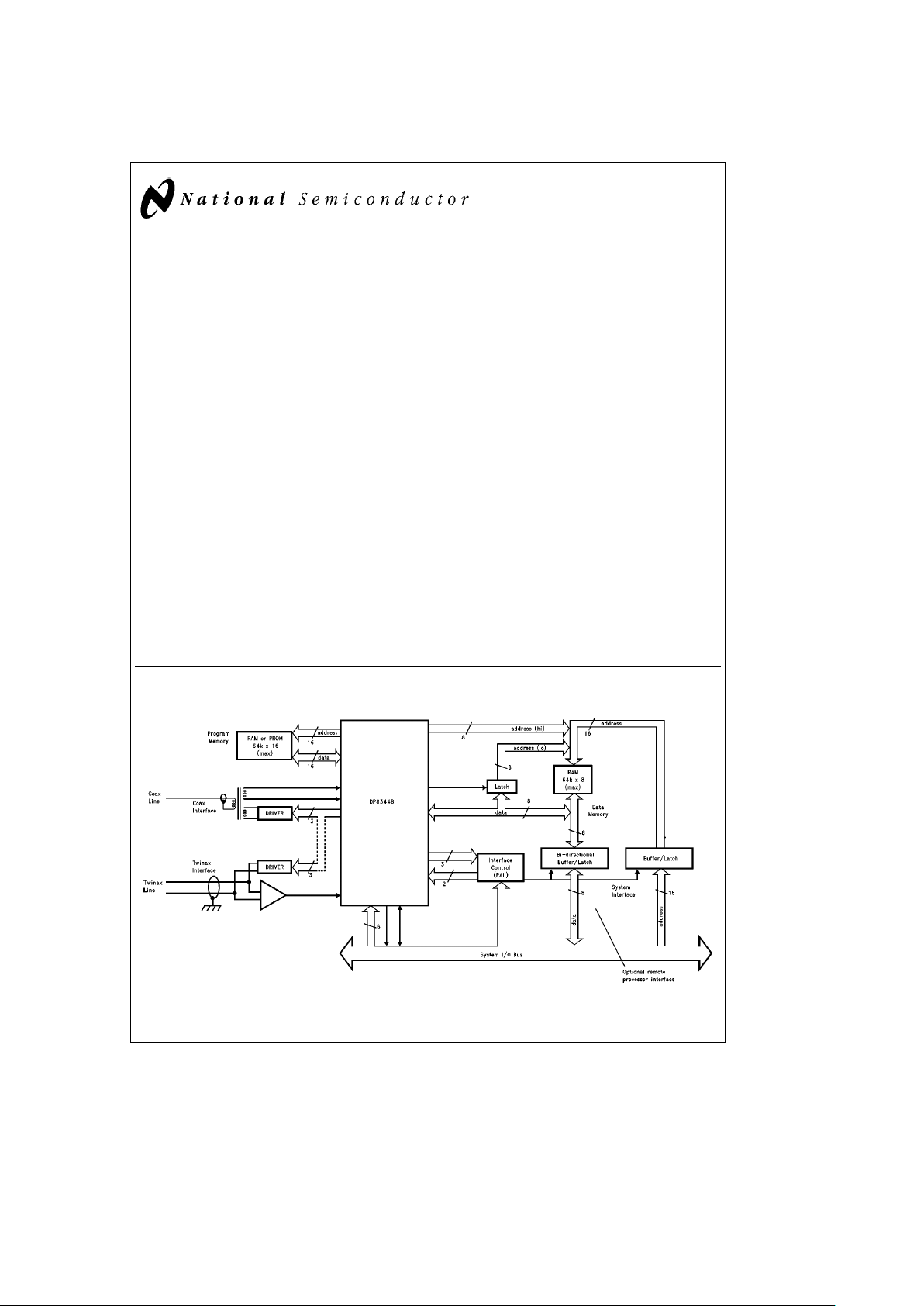
A typical system is shown below. Both coax and twinax line
interfaces are shown, as well as an example of the (optional) remote processor interface.
Features
Transceiver
Y
Software configurable for 3270, 3299, 5250 and general
8-bit protocols
Y
Fully registered status and control
Y
On-chip analog line receiver
Processor
Y
20 MHz clock (50 ns T-states)
Y
Max. instruction cycle: 200 ns
Y
33 instruction types (50 total opcodes)
Y
ALU and barrel shifter
Y
64k x 8 data memory address range
Y
64k x 16 program memory address range
(note: typical system requires
k
2k program memory)
Y
Programmable wait states
Y
Soft-loadable program memory
Y
Interrupt and subroutine capability
Y
Stand alone or host operation
Y
Flexible bus interface with on-chip arbitration logic
General
Y
Low power microCMOS; typ. I
CC
e
25 mA at 20 MHz
Y
84-pin plastic leaded chip carrier (PLCC) package
Block Diagram
Typical BCP System
TL/F/9336– 51
FIGURE 1
BCPÉand TRI-STATEÉare registered trademarks of National Semiconductor Corporation.
IBM
É
is a registered trademark of International Business Machines Corporation.
C
1995 National Semiconductor Corporation RRD-B30M105/Printed in U. S. A.
Page 2

The DP8344B is an enhanced version of the DP8344A, exhibiting improved switching performance and additional
functionality. The device has been been characterized in a number of applications and found to be a compatible
replacement for the DP8344A. Differences between the DP8344A and DP8344B are noted by shading of the text on the
pages of this data sheet. For more information, refer to Section 6.6.
Note: In this document[XXX]denotes a control or status bit in a register,
À
YYYÓdenotes a register.
Table of Contents
1.0 COMMUNICATIONS PROCESSOR OVERVIEW
1.1 Communications Protocols
1.2 Internal Architecture Overview
1.3 Timing Overview
1.4 Data Flow
1.5 Remote Interface Overview
2.0 CPU DESCRIPTION
2.1 CPU Architectural Description
2.1.1 Register Set
2.1.1.1 Banked Registers
2.1.1.2 Timing Control Registers
2.1.1.3 Interrupt Control Registers
2.1.1.4 Timer Registers
2.1.1.5 Transceiver Registers
2.1.1.6 Condition Code/Remote Handshaking
Register
2.1.1.7 Index Registers
2.1.1.8 Stack Registers
2.1.2 Timer
2.1.2.1 Timer Operation
2.1.3 Instruction Set
2.1.3.1 Harvard Architecture Implications
2.1.3.2 Addressing Modes
2.1.3.3 Instruction Set Overview
2.2 Functional Description
2.2.1 ALU
2.2.2 Timing
2.2.3 Interrupts
2.2.4 Oscillator
3.0 TRANSCEIVER
3.1 Transceiver Architectural Description
3.1.1 Protocols
3.1.1.1 IBM 3270
3.1.1.2 IBM 3299
3.1.1.3 IBM 5250
3.1.1.4 General Purpose 8-Bit
3.2 Transceiver Functional Description
3.2.1 Transmitter
3.2.2 Receiver
3.2.3 Transceiver Interrupts
3.2.4 Protocol Modes
3.2.5 Line Interface
3.2.5.1 3270 Line Interface
3.2.5.2 5250 Line Interface
4.0 REMOTE INTERFACE AND ARBITRATION SYSTEM
(RIAS)
4.1 RIAS Architectural Description
4.1.1 Remote Arbitration Phases
4.1.2 Access Types
4.1.3 Interface Modes
4.1.4 Execution Control
4.2 RIAS Functional Description
4.2.1 Buffered Read
4.2.2 Latched Read
4.2.3 Slow Buffered Write
4.2.4 Fast Buffered Write
4.2.5 Latched Write
4.2.6 Remote Rest Time
2
Page 3

Table of Contents (Continued)
5.0 DEVICE SPECIFICATIONS
5.1 Pin Description
5.1.1 Timing/Control Signals
5.1.2 Instruction Memory Interface
5.1.3 Data Memory Interface
5.1.4 Transceiver Interface
5.1.5 Remote Interface
5.1.6 External Interrupts
5.2 Absolute Maximum Ratings
5.3 Operating Conditions
5.4 Electrical Characteristics
5.5 Switching Characteristics
5.5.1 Definitions
5.5.2 Timing Tables and Figures
6.0 REFERENCE SECTION
6.1 Instruction Set Reference
6.2 Register Set Reference
6.2.1 Bit Index
6.2.2 Register Description
6.2.3 Bit Definition Tables
6.2.3.1 Processor
6.2.3.2 Transceiver
6.3 Remote Interface Reference
6.4 Development Tools
6.4.1 Assembler System
6.4.2 Development Kit
6.4.3 Multi-Protocol Adapter Design/Evaluation Kit
6.4.4 Inverse Assembler
6.5 3rd Party Suppliers
6.5.1 Crystal
6.5.2 System Development Tools
6.6 DP8344A Compatibility Guide
6.6.1 CPU Timing Changes
6.6.2 Additional Functionality
6.6.2.1 4 T-state Read
6.6.2.2 A/AD Reset State
6.6.2.3 RIC
6.6.2.4 Transceiver
6.7 Reported Bugs
6.7.1 History
6.7.2 LJMP, LCALL Address Decode
6.7.2.1 Suggested Work-around
6.8 Glossary
6.9 Physical Dimensions
3
Page 4

List of Illustrations
Block Diagram of Typical BCP System АААААААААААААААААААААААААААААААААААААААААААААААААААААААААААААААААААААААААААААА1
Biphase EncodingАААААААААААААААААААААААААААААААААААААААААААААААААААААААААААААААААААААААААААААААААААААААААААААА1-1
IBM 3270 Message FormatАААААААААААААААААААААААААААААААААААААААААААААААААААААААААААААААААААААААААААААААААААААА1-2
Simplified Block DiagramАААААААААААААААААААААААААААААААААААААААААААААААААААААААААААААААААААААААААААААААААААААААА1-3
Memory Configuration АААААААААААААААААААААААААААААААААААААААААААААААААААААААААААААААААААААААААААААААААААААААААА1-4
Effect of Memory Wait States on TimingААААААААААААААААААААААААААААААААААААААААААААААААААААААААААААААААААААААААААА1-5
Register to Register Internal Data Flow АААААААААААААААААААААААААААААААААААААААААААААААААААААААААААААААААААААААААА1-6a
Data Memory WRITE Data Flow АААААААААААААААААААААААААААААААААААААААААААААААААААААААААААААААААААААААААААААААА1-6b
Data Memory READ Data Flow ААААААААААААААААААААААААААААААААААААААААААААААААААААААААААААААААААААААААААААААААА1-6c
WRITE to Transmitter Data Flow АААААААААААААААААААААААААААААААААААААААААААААААААААААААААААААААААААААААААААААААА1-6d
READ from Receiver Data FlowААААААААААААААААААААААААААААААААААААААААААААААААААААААААААААААААААААААААААААААААА1-6e
Load Immediate Data Data FlowААААААААААААААААААААААААААААААААААААААААААААААААААААААААААААААААААААААААААААААААА1-6f
Basic Remote Interface ААААААААААААААААААААААААААААААААААААААААААААААААААААААААААААААААААААААААААААААААААААААААА1-7
Register Map АААААААААААААААААААААААААААААААААААААААААААААААААААААААААААААААААААААААААААААААААААААААААААААААААА2-1
Timer Block Diagram ААААААААААААААААААААААААААААААААААААААААААААААААААААААААААААААААААААААААААААААААААААААААААА2-2
Timer Interrupt DiagramААААААААААААААААААААААААААААААААААААААААААААААААААААААААААААААААААААААААААААААААААААААААА2-3
Index Register MapААААААААААААААААААААААААААААААААААААААААААААААААААААААААААААААААААААААААААААААААААААААААААААА2-4
Coding Examples of Equivalent Conditional Jump Instructions ААААААААААААААААААААААААААААААААААААААААААААААААААААААА2-5
JRMK Instruction Example АААААААААААААААААААААААААААААААААААААААААААААААААААААААААААААААААААААААААААААААААААААА2-6
Condition Code Register ALU Flags АААААААААААААААААААААААААААААААААААААААААААААААААААААААААААААААААААААААААААААА2-7
Carry and Overflow Calculations ААААААААААААААААААААААААААААААААААААААААААААААААААААААААААААААААААААААААААААААААА2-8
Shifts’ Effect on Carry АААААААААААААААААААААААААААААААААААААААААААААААААААААААААААААААААААААААААААААААААААААААААА2-9
Rotates’ Effect on Carry ААААААААААААААААААААААААААААААААААААААААААААААААААААААААААААААААААААААААААААААААААААААА2-10
Multi-Byte Arithmetic Instruction Sequences АААААААААААААААААААААААААААААААААААААААААААААААААААААААААААААААААААААА2-11
CPU-CLK Synchronization with X1 АААААААААААААААААААААААААААААААААААААААААААААААААААААААААААААААААААААААААААААА2-12
Changing from OCLK/2 to OCLKАААААААААААААААААААААААААААААААААААААААААААААААААААААААААААААААААААААААААААААААА2-13
Two T-state Instruction АААААААААААААААААААААААААААААААААААААААААААААААААААААААААААААААААААААААААААААААААААААААА2-14
Three T-state Instruction ААААААААААААААААААААААААААААААААААААААААААААААААААААААААААААААААААААААААААААААААААААААА2-15
Three T-state Data Memory Write Instruction ААААААААААААААААААААААААААААААААААААААААААААААААААААААААААААААААААААА2-16
Three T-state Data Memory Read Instruction ААААААААААААААААААААААААААААААААААААААААААААААААААААААААААААААААААААА2-17
Four T-state Data Memory Read Instruction АААААААААААААААААААААААААААААААААААААААААААААААААААААААААААААААААААААА2-18
Four T-state Program Control Instruction ААААААААААААААААААААААААААААААААААААААААААААААААААААААААААААААААААААААААА2-19
Four T-state Two Word Instruction АААААААААААААААААААААААААААААААААААААААААААААААААААААААААААААААААААААААААААААА2-20
Data Memory Write with One Wait State ААААААААААААААААААААААААААААААААААААААААААААААААААААААААААААААААААААААААА2-21
Data Memory Read with One Wait State ААААААААААААААААААААААААААААААААААААААААААААААААААААААААААААААААААААААААА2-22
Data Memory Read with Two Wait States АААААААААААААААААААААААААААААААААААААААААААААААААААААААААААААААААААААААА2-23
Two T-state Instruction with Two Wait States ААААААААААААААААААААААААААААААААААААААААААААААААААААААААААААААААААААА2-24
Four T-state Instruction with One Wait State АААААААААААААААААААААААААААААААААААААААААААААААААААААААААААААААААААААА2-25
Data Memory Access Wait TimingААААААААААААААААААААААААААААААААААААААААААААААААААААААААААААААААААААААААААААААА2-26
Two T-state Instruction WAIT Timing АААААААААААААААААААААААААААААААААААААААААААААААААААААААААААААААААААААААААААА2-27
Three T-state Program Control Instruction WAIT Timing АААААААААААААААААААААААААААААААААААААААААААААААААААААААААААА2-28
Four T-state Program Control Instruction WAIT Timing ААААААААААААААААААААААААААААААААААААААААААААААААААААААААААААА2-29
LOCK Timing ААААААААААААААААААААААААААААААААААААААААААААААААААААААААААААААААААААААААААААААААААААААААААААААААА2-30
LOCK Timing with One Wait State ААААААААААААААААААААААААААААААААААААААААААААААААААААААААААААААААААААААААААААААА2-31
CPU Start-Up Timing АААААААААААААААААААААААААААААААААААААААААААААААААААААААААААААААААААААААААААААААААААААААААА2-32
Functional State Diagram of CPU Timing ААААААААААААААААААААААААААААААААААААААААААААААААААААААААААААААААААААААААА2-33
Interrupt TimingААААААААААААААААААААААААААААААААААААААААААААААААААААААААААААААААААААААААААААААААААААААААААААААА2-34
DP8344B Operation with Crystal АААААААААААААААААААААААААААААААААААААААААААААААААААААААААААААААААААААААААААААААА2-35
DP8344B Operation with External Clock ААААААААААААААААААААААААААААААААААААААААААААААААААААААААААААААААААААААААА2-36
4
Page 5

List of Illustrations (Continued)
System Block Diagram, Showing Details of Line Interface ААААААААААААААААААААААААААААААААААААААААААААААААААААААААААА3-1
Biphase EncodingАААААААААААААААААААААААААААААААААААААААААААААААААААААААААААААААААААААААААААААААААААААААААААААА3-2
3270/3299 Protocol Framing Format ААААААААААААААААААААААААААААААААААААААААААААААААААААААААААААААААААААААААААААА3-3
5250 Protocol Framing FormatААААААААААААААААААААААААААААААААААААААААААААААААААААААААААААААААААААААААААААААААААА3-4
General Purpose 8-Bit Protocol Framing FormatАААААААААААААААААААААААААААААААААААААААААААААААААААААААААААААААААААА3-5
Block Diagram of Transceiver, Showing CPU Interface АААААААААААААААААААААААААААААААААААААААААААААААААААААААААААААА3-6
Transmitter Output ААААААААААААААААААААААААААААААААААААААААААААААААААААААААААААААААААААААААААААААААААААААААААААА3-7
Timing of Receiver Flags Relative to Incoming Data АААААААААААААААААААААААААААААААААААААААААААААААААААААААААААААААА3-8
3270, 3299 Frame Assembly/Disassembly DescriptionАААААААААААААААААААААААААААААААААААААААААААААААААААААААААААААА3-9
5250 Frame Assembly/Disassembly Description АААААААААААААААААААААААААААААААААААААААААААААААААААААААААААААААААА3-10
General Purpose 8-Bit Frame Assembly/Disassembly Description ААААААААААААААААААААААААААААААААААААААААААААААААААА3-11
BCP Receiver DesignАААААААААААААААААААААААААААААААААААААААААААААААААААААААААААААААААААААААААААААААААААААААААА3-12
BCP Driver Design АААААААААААААААААААААААААААААААААААААААААААААААААААААААААААААААААААААААААААААААААААААААААААА3-13
BCP Coax/Twisted Pair Front End АААААААААААААААААААААААААААААААААААААААААААААААААААААААААААААААААААААААААААААА3-14
5250 Line Interface SchematicАААААААААААААААААААААААААААААААААААААААААААААААААААААААААААААААААААААААААААААААААА3-15
Remote Interface Processor ААААААААААААААААААААААААААААААААААААААААААААААААААААААААААААААААААААААААААААААААААААА4-1
Remote Interface Control Register ААААААААААААААААААААААААААААААААААААААААААААААААААААААААААААААААААААААААААААААА4-2
Generic Remote Access АААААААААААААААААААААААААААААААААААААААААААААААААААААААААААААААААААААААААААААААААААААААА4-3
Generic RIC Access АААААААААААААААААААААААААААААААААААААААААААААААААААААААААААААААААААААААААААААААААААААААААААА4-4
Memory Select Bits in
À
RICУААААААААААААААААААААААААААААААААААААААААААААААААААААААААААААААААААААААААААААААААААААА4-5
Generic DMEM Access ААААААААААААААААААААААААААААААААААААААААААААААААААААААААААААААААААААААААААААААААААААААААА4-6
Generic PC AccessААААААААААААААААААААААААААААААААААААААААААААААААААААААААААААААААААААААААААААААААААААААААААААА4-7
Generic IMEM Access АААААААААААААААААААААААААААААААААААААААААААААААААААААААААААААААААААААААААААААААААААААААААА4-8
Read from Remote Processor ААААААААААААААААААААААААААААААААААААААААААААААААААААААААААААААААААААААААААААААААААА4-9
Buffered Write from Remote Processor АААААААААААААААААААААААААААААААААААААААААААААААААААААААААААААААААААААААААА4-10
Latched Write from Remote ProcessorААААААААААААААААААААААААААААААААААААААААААААААААААААААААААААААААААААААААААА4-11
Minimum BCP/Remote Processor Interface АААААААААААААААААААААААААААААААААААААААААААААААААААААААААААААААААААААА4-12
Interface Mode Bits ААААААААААААААААААААААААААААААААААААААААААААААААААААААААААААААААААААААААААААААААААААААААААА4-13
Flow Chart of Buffered Read Mode АААААААААААААААААААААААААААААААААААААААААААААААААААААААААААААААААААААААААААААА4-14
Buffered Read of Data Memory by Remote Processor ААААААААААААААААААААААААААААААААААААААААААААААААААААААААААААА4-15
Flow Chart of Latched Read Mode АААААААААААААААААААААААААААААААААААААААААААААААААААААААААААААААААААААААААААААА4-16
Latched Read of Data Memory by Remote Processor АААААААААААААААААААААААААААААААААААААААААААААААААААААААААААААА4-17
Flow Chart of Slow Buffered Write Mode ААААААААААААААААААААААААААААААААААААААААААААААААААААААААААААААААААААААААА4-18
Slow Buffered Write to Data Memory by Remote ProcessorААААААААААААААААААААААААААААААААААААААААААААААААААААААААА4-19
Flow Chart of Fast Buffered Write ModeАААААААААААААААААААААААААААААААААААААААААААААААААААААААААААААААААААААААААА4-20
Fast Buffered Write to Data Memory by Remote Processor ААААААААААААААААААААААААААААААААААААААААААААААААААААААААА4-21
Flow Chart of Latched Write Mode АААААААААААААААААААААААААААААААААААААААААААААААААААААААААААААААААААААААААААААА4-22
Latched Write to Data Memory by Remote Processor АААААААААААААААААААААААААААААААААААААААААААААААААААААААААААААА4-23
Mistaking Two Remote Accesses as Only OneАААААААААААААААААААААААААААААААААААААААААААААААААААААААААААААААААААА4-24
Remote Rest Time for All Modes Except Latched Write АААААААААААААААААААААААААААААААААААААААААААААААААААААААААААА4-25
Rest Time for Latched Write Mode АААААААААААААААААААААААААААААААААААААААААААААААААААААААААААААААААААААААААААААА4-26
DP8344B Top ViewААААААААААААААААААААААААААААААААААААААААААААААААААААААААААААААААААААААААААААААААААААААААААААА5-1
Switching Characteristic Measurement Waveforms ААААААААААААААААААААААААААААААААААААААААААААААААААААААААААААААААА5-2
Data Memory Read Timing АААААААААААААААААААААААААААААААААААААААААААААААААААААААААААААААААААААААААААААААААААААА5-3
Data Memory Write Timing АААААААААААААААААААААААААААААААААААААААААААААААААААААААААААААААААААААААААААААААААААААА5-4
Instruction Memory Timing АААААААААААААААААААААААААААААААААААААААААААААААААААААААААААААААААААААААААААААААААААААА5-5
Clock Timing АААААААААААААААААААААААААААААААААААААААААААААААААААААААААААААААААААААААААААААААААААААААААААААААААА5-6
5
Page 6

List of Illustrations (Continued)
Transceiver Timing ААААААААААААААААААААААААААААААААААААААААААААААААААААААААААААААААААААААААААААААААААААААААААААА5-7
Analog and DATA-IN Timing ААААААААААААААААААААААААААААААААААААААААААААААААААААААААААААААААААААААААААААААААААААА5-8
Interrupt Timing АААААААААААААААААААААААААААААААААААААААААААААААААААААААААААААААААААААААААААААААААААААААААААААААА5-9
Control Pin Timing АААААААААААААААААААААААААААААААААААААААААААААААААААААААААААААААААААААААААААААААААААААААААААА5-10
Buffered Read of PC, RIC АААААААААААААААААААААААААААААААААААААААААААААААААААААААААААААААААААААААААААААААААААААА5-11
Buffered Read of DMEM ААААААААААААААААААААААААААААААААААААААААААААААААААААААААААААААААААААААААААААААААААААААА5-12
Buffered Read of IMEM АААААААААААААААААААААААААААААААААААААААААААААААААААААААААААААААААААААААААААААААААААААААА5-13
Latched Read of PC, RIC АААААААААААААААААААААААААААААААААААААААААААААААААААААААААААААААААААААААААААААААААААААА5-14
Latched Read of DMEM ААААААААААААААААААААААААААААААААААААААААААААААААААААААААААААААААААААААААААААААААААААААА5-15
Latched Read of IMEM АААААААААААААААААААААААААААААААААААААААААААААААААААААААААААААААААААААААААААААААААААААААА5-16
Slow Buffered Write of PC, RIC ААААААААААААААААААААААААААААААААААААААААААААААААААААААААААААААААААААААААААААААААА5-17
Slow Buffered Write of DMEM АААААААААААААААААААААААААААААААААААААААААААААААААААААААААААААААААААААААААААААААААА5-18
Slow Buffered Write of IMEM ААААААААААААААААААААААААААААААААААААААААААААААААААААААААААААААААААААААААААААААААААА5-19
Fast Buffered Write of PC, RICАААААААААААААААААААААААААААААААААААААААААААААААААААААААААААААААААААААААААААААААААА5-20
Fast Buffered Write of DMEMААААААААААААААААААААААААААААААААААААААААААААААААААААААААААААААААААААААААААААААААААА5-21
Fast Buffered Write of IMEM ААААААААААААААААААААААААААААААААААААААААААААААААААААААААААААААААААААААААААААААААААА5-22
Latched Write of PC, RICААААААААААААААААААААААААААААААААААААААААААААААААААААААААААААААААААААААААААААААААААААААА5-23
Latched Write of DMEM ААААААААААААААААААААААААААААААААААААААААААААААААААААААААААААААААААААААААААААААААААААААА5-24
Latched Write of IMEM АААААААААААААААААААААААААААААААААААААААААААААААААААААААААААААААААААААААААААААААААААААААА5-25
Remote Rest Times ААААААААААААААААААААААААААААААААААААААААААААААААААААААААААААААААААААААААААААААААААААААААААА5-26
Remote Interface WAIT Timing ААААААААААААААААААААААААААААААААААААААААААААААААААААААААААААААААААААААААААААААААА5-27
WAIT Timing after Remote Access АААААААААААААААААААААААААААААААААААААААААААААААААААААААААААААААААААААААААААААА5-28
Instruction Memory Bus Timing for 2 T-state Instructions АААААААААААААААААААААААААААААААААААААААААААААААААААААААААААА6-1
Instruction Memory Bus Timing for 3 T-state Instructions АААААААААААААААААААААААААААААААААААААААААААААААААААААААААААА6-2
Instruction Memory Bus Timing for (2
a
2) T-state Instructions АААААААААААААААААААААААААААААААААААААААААААААААААААААААА6-3
Instruction Memory Bus Timing for 4 T-state Instructions АААААААААААААААААААААААААААААААААААААААААААААААААААААААААААА6-4
Instruction/Data Memory Bus Timing for Data Memory Read[4TR
]
e
0ААААААААААААААААААААААААААААААААААААААААААААААА6-5
Instruction/Data Memory Bus Timing for Data Memory Read[4TR
]
e
1ААААААААААААААААААААААААААААААААААААААААААААААА6-6
Instruction/Data Memory Bus Timing for Data Memory WriteААААААААААААААААААААААААААААААААААААААААААААААААААААААААА6-7
List of Tables
Register Addressing Mode Notations ААААААААААААААААААААААААААААААААААААААААААААААААААААААААААААААААААААААААААААА2-1
Immediate Addressing Mode Notations ААААААААААААААААААААААААААААААААААААААААААААААААААААААААААААААААААААААААААА2-2
Index Register Addressing Mode Notations АААААААААААААААААААААААААААААААААААААААААААААААААААААААААААААААААААААААА2-3
Relative Index Register Mode NotationsААААААААААААААААААААААААААААААААААААААААААААААААААААААААААААААААААААААААААА2-4
Data Movement NotationsААААААААААААААААААААААААААААААААААААААААААААААААААААААААААААААААААААААААААААААААААААААА2-5
Integer Arithmetic Instruction АААААААААААААААААААААААААААААААААААААААААААААААААААААААААААААААААААААААААААААААААААА2-6
Logic Instructions АААААААААААААААААААААААААААААААААААААААААААААААААААААААААААААААААААААААААААААААААААААААААААААА2-7
Shift and Rotate InstructionsААААААААААААААААААААААААААААААААААААААААААААААААААААААААААААААААААААААААААААААААААААА2-8
Comparison Instructions АААААААААААААААААААААААААААААААААААААААААААААААААААААААААААААААААААААААААААААААААААААААА2-9
Unconditional Jump Instructions АААААААААААААААААААААААААААААААААААААААААААААААААААААААААААААААААААААААААААААААА2-10
Conditional Relative Jump InstructionsААААААААААААААААААААААААААААААААААААААААААААААААААААААААААААААААААААААААААА2-11
‘‘f’’ FlagsААААААААААААААААААААААААААААААААААААААААААААААААААААААААААААААААААААААААААААААААААААААААААААААААААААА2-12
‘‘cc’’ Conditions Tested АААААААААААААААААААААААААААААААААААААААААААААААААААААААААААААААААААААААААААААААААААААААА2-13
Conditional Absolute Jump Instructions АААААААААААААААААААААААААААААААААААААААААААААААААААААААААААААААААААААААААА2-14
JRMK Instruction ААААААААААААААААААААААААААААААААААААААААААААААААААААААААААААААААААААААААААААААААААААААААААААА2-15
Unconditional Call InstructionsАААААААААААААААААААААААААААААААААААААААААААААААААААААААААААААААААААААААААААААААААА2-16
Conditional Call Instructions АААААААААААААААААААААААААААААААААААААААААААААААААААААААААААААААААААААААААААААААААААА2-17
Unconditional Return Instruction АААААААААААААААААААААААААААААААААААААААААААААААААААААААААААААААААААААААААААААААА2-18
Conditional Return Instruction АААААААААААААААААААААААААААААААААААААААААААААААААААААААААААААААААААААААААААААААААА2-19
TRAP InstructionАААААААААААААААААААААААААААААААААААААААААААААААААААААААААААААААААААААААААААААААААААААААААААААА2-20
EXX Instruction ААААААААААААААААААААААААААААААААААААААААААААААААААААААААААААААААААААААААААААААААААААААААААААААА2-21
6
Page 7

List of Tables (Continued)
Unsigned Comparison Results АААААААААААААААААААААААААААААААААААААААААААААААААААААААААААААААААААААААААААААААААА2-22
Signed Comparison Results АААААААААААААААААААААААААААААААААААААААААААААААААААААААААААААААААААААААААААААААААААА2-23
Data Memory Wait States АААААААААААААААААААААААААААААААААААААААААААААААААААААААААААААААААААААААААААААААААААААА2-24
Instruction Memory Wait States ААААААААААААААААААААААААААААААААААААААААААААААААААААААААААААААААААААААААААААААААА2-25
BIRQ Control Summary АААААААААААААААААААААААААААААААААААААААААААААААААААААААААААААААААААААААААААААААААААААААА2-26
À
ICRУInterrupt Mask Bits and Interrupt PriorityАААААААААААААААААААААААААААААААААААААААААААААААААААААААААААААААААААА2-27
Interrupt Vector Generation АААААААААААААААААААААААААААААААААААААААААААААААААААААААААААААААААААААААААААААААААААА2-28
Recommended Crystal ParametersАААААААААААААААААААААААААААААААААААААААААААААААААААААААААААААААААААААААААААААА2-29
Protocol Mode Definitions ААААААААААААААААААААААААААААААААААААААААААААААААААААААААААААААААААААААААААААААААААААААА3-1
Transceiver Interrupts АААААААААААААААААААААААААААААААААААААААААААААААААААААААААААААААААААААААААААААААААААААААААА3-2
Receiver Interrupts ААААААААААААААААААААААААААААААААААААААААААААААААААААААААААААААААААААААААААААААААААААААААААААА3-3
Decode of 3270 Coax Commands АААААААААААААААААААААААААААААААААААААААААААААААААААААААААААААААААААААААААААААААА3-4
RIAS Inputs and Outputs АААААААААААААААААААААААААААААААААААААААААААААААААААААААААААААААААААААААААААААААААААААААА4-1
Note: To match Timing table number with appropriate Timing illustration, Tables 5-1 and 5-2 are purposely omitted.
Data Memory Read Timing АААААААААААААААААААААААААААААААААААААААААААААААААААААААААААААААААААААААААААААААААААААА5-3
Data Memory Write Timing АААААААААААААААААААААААААААААААААААААААААААААААААААААААААААААААААААААААААААААААААААААА5-4
Instruction Memory Timing АААААААААААААААААААААААААААААААААААААААААААААААААААААААААААААААААААААААААААААААААААААА5-5
Clock Timing АААААААААААААААААААААААААААААААААААААААААААААААААААААААААААААААААААААААААААААААААААААААААААААААААА5-6
Transceiver Timing ААААААААААААААААААААААААААААААААААААААААААААААААААААААААААААААААААААААААААААААААААААААААААААА5-7
Analog and DATA-IN Timing ААААААААААААААААААААААААААААААААААААААААААААААААААААААААААААААААААААААААААААААААААААА5-8
Interrupt Timing АААААААААААААААААААААААААААААААААААААААААААААААААААААААААААААААААААААААААААААААААААААААААААААААА5-9
Control Pin Timing АААААААААААААААААААААААААААААААААААААААААААААААААААААААААААААААААААААААААААААААААААААААААААА5-10
Buffered Read of PC, RIC АААААААААААААААААААААААААААААААААААААААААААААААААААААААААААААААААААААААААААААААААААААА5-11
Buffered Read of DMEM ААААААААААААААААААААААААААААААААААААААААААААААААААААААААААААААААААААААААААААААААААААААА5-12
Buffered Read of IMEM АААААААААААААААААААААААААААААААААААААААААААААААААААААААААААААААААААААААААААААААААААААААА5-13
Latched Read of PC, RIC АААААААААААААААААААААААААААААААААААААААААААААААААААААААААААААААААААААААААААААААААААААА5-14
Latched Read of DMEM ААААААААААААААААААААААААААААААААААААААААААААААААААААААААААААААААААААААААААААААААААААААА5-15
Latched Read of IMEM АААААААААААААААААААААААААААААААААААААААААААААААААААААААААААААААААААААААААААААААААААААААА5-16
Slow Buffered Write of PC, RIC ААААААААААААААААААААААААААААААААААААААААААААААААААААААААААААААААААААААААААААААААА5-17
Slow Buffered Write of DMEM АААААААААААААААААААААААААААААААААААААААААААААААААААААААААААААААААААААААААААААААААА5-18
Slow Buffered Write of IMEM ААААААААААААААААААААААААААААААААААААААААААААААААААААААААААААААААААААААААААААААААААА5-19
Fast Buffered Write of PC, RICАААААААААААААААААААААААААААААААААААААААААААААААААААААААААААААААААААААААААААААААААА5-20
Fast Buffered Write of DMEMААААААААААААААААААААААААААААААААААААААААААААААААААААААААААААААААААААААААААААААААААА5-21
Fast Buffered Write of IMEM ААААААААААААААААААААААААААААААААААААААААААААААААААААААААААААААААААААААААААААААААААА5-22
Latched Write of PC, RICААААААААААААААААААААААААААААААААААААААААААААААААААААААААААААААААААААААААААААААААААААААА5-23
Latched Write of DMEM ААААААААААААААААААААААААААААААААААААААААААААААААААААААААААААААААААААААААААААААААААААААА5-24
Latched Write of IMEM АААААААААААААААААААААААААААААААААААААААААААААААААААААААААААААААААААААААААААААААААААААААА5-25
Remote Rest Times ААААААААААААААААААААААААААААААААААААААААААААААААААААААААААААААААААААААААААААААААААААААААААА5-26
Remote Interface WAIT Timing ААААААААААААААААААААААААААААААААААААААААААААААААААААААААААААААААААААААААААААААААА5-27
WAIT Timing after Remote Access АААААААААААААААААААААААААААААААААААААААААААААААААААААААААААААААААААААААААААААА5-28
Notational Conventions for Instruction SetААААААААААААААААААААААААААААААААААААААААААААААААААААААААААААААААААААААААА6-1
Instructions vs T-states, Affected Flags and Bus Timing ААААААААААААААААААААААААААААААААААААААААААААААААААААААААААААА6-2
Instruction Opcodes АААААААААААААААААААААААААААААААААААААААААААААААААААААААААААААААААААААААААААААААААААААААААААА6-3
DP8344B Application Notes ААААААААААААААААААААААААААААААААААААААААААААААААААААААААААААААААААААААААААААААААААААА6-4
7
Page 8
1.0 Communications Processor Introduction
The increased demand for computer connectivity has driven
National Semiconductor to develop the next generation of
special purpose microprocessors. The DP8344B is the first
example of a ‘‘Communications Processor’’ for the IBM environment. It integrates a very fast, full function microprocessor with highly specialized transceiver circuitry. The combination of speed, power, and features allows the designer
to easily implement a state-of-the-art communications interface. Typical applications for a communications processor
are terminal emulation boards for PCs, stand-alone terminals, printer interfaces, and cluster controllers.
The transceiver is designed to simplify the handling of specific communication protocols. This feature makes it possible to quickly develop interfaces and software with little concern for the ‘‘housekeeping’’ details of the protocol being
used.
1.1 COMMUNICATIONS PROTOCOLS
A communication protocol is a set of rules which defines the
physical, electrical, and software specifications required to
successfully transfer data between two systems.
The physical specification includes the network architecture, as well as the type of connecting medium, the connectors used, and the maximum distance between connections.
Networks may be configured in ‘‘loops,’’ ‘‘stars,’’ or ‘‘daisy
chains,’’ and they often use standard coaxial or twisted-pair
cable.
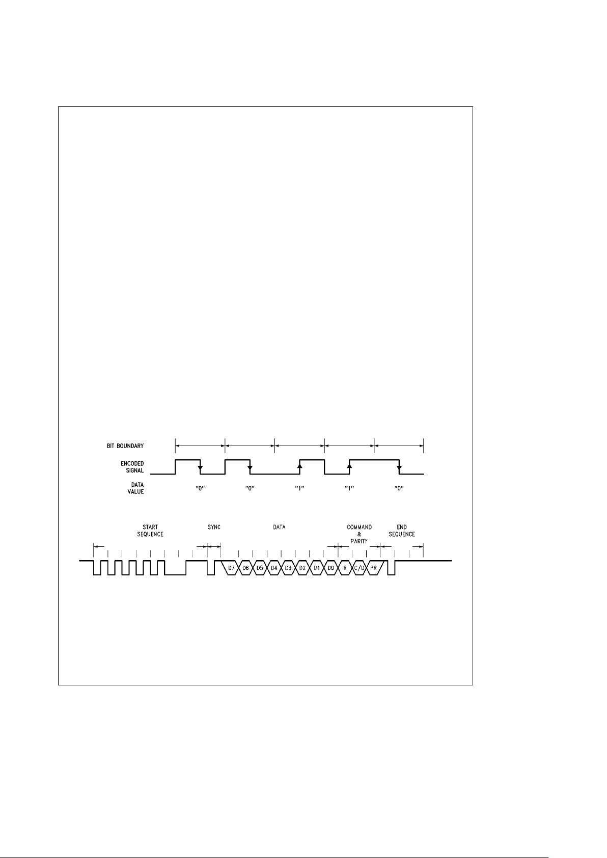
The electrical specification includes the polarity and amplitude of the signal, the frequency (bit rate), and encoding
technique. One common method of encoding is called ‘‘biphase’’ or ‘‘Manchester II.’’ This technique combines the
clock and data information into one transmission by encoding data as a ‘‘mid-bit’’ transition.
Figure 1-1
shows how the
data transition is related to the bit boundary in a typical
transmission. The polarity of the ‘‘mid-bit’’ transition en-
codes the data value, other transitions lie on bit boundaries.
Bit boundaries are not always indicated by transitions, so
techniques employing start sequences and sync bits are
used with bi-phase transmissions to ensure proper frame
alignment and synchronization.
The software specification covers the use of start sequences and sync bits, as well as defining the message
format. Parity bits may be used to ensure data integrity. The
message format is the ‘‘language’’ that is used to exchange
information across the connecting medium. It defines command and control words, response times, and expected responses.
The DP8344B Bi-phase Communications Processor supports both the IBM 3270 and 5250 communication protocols, as well as IBM 3299 and a general purpose 8-bit protocol. The specialized transceiver is combined with a microprocessor whose instruction set is optimized for use in a
communications environment. This makes the DP8344 a
powerful single-chip solution to a wide range of communication applications.
An example of an IBM 3270 message is shown in
Figure
1-2
. The transmission begins with a very specific start sequence and sync pulse for synchronization. This is followed
by the data, command, and parity bits. Finally, the end sequence defines the end of the transmission.
The IBM 3270 and 5250 are two widely used protocols. The
3270 protocol was developed for the 370 class mainframe,
and it employs coaxial cable in a ‘‘star’’ configuration. The
5250 protocol was developed for the System/3x machines,
and it uses a ‘‘daisy-chain’’ of twin-ax cable. A good overview of both of these environments may be found in the
‘‘Multi-Protocol Adapter System User Guide’’ from National
Semiconductor, and in the Transceiver section of this document.
TL/F/9336– B7
FIGURE 1-1. Biphase Encoding
TL/F/9336– B8
FIGURE 1-2. IBM 3270 Message Format
8
Page 9
1.0 Communications Processor Introduction (Continued)
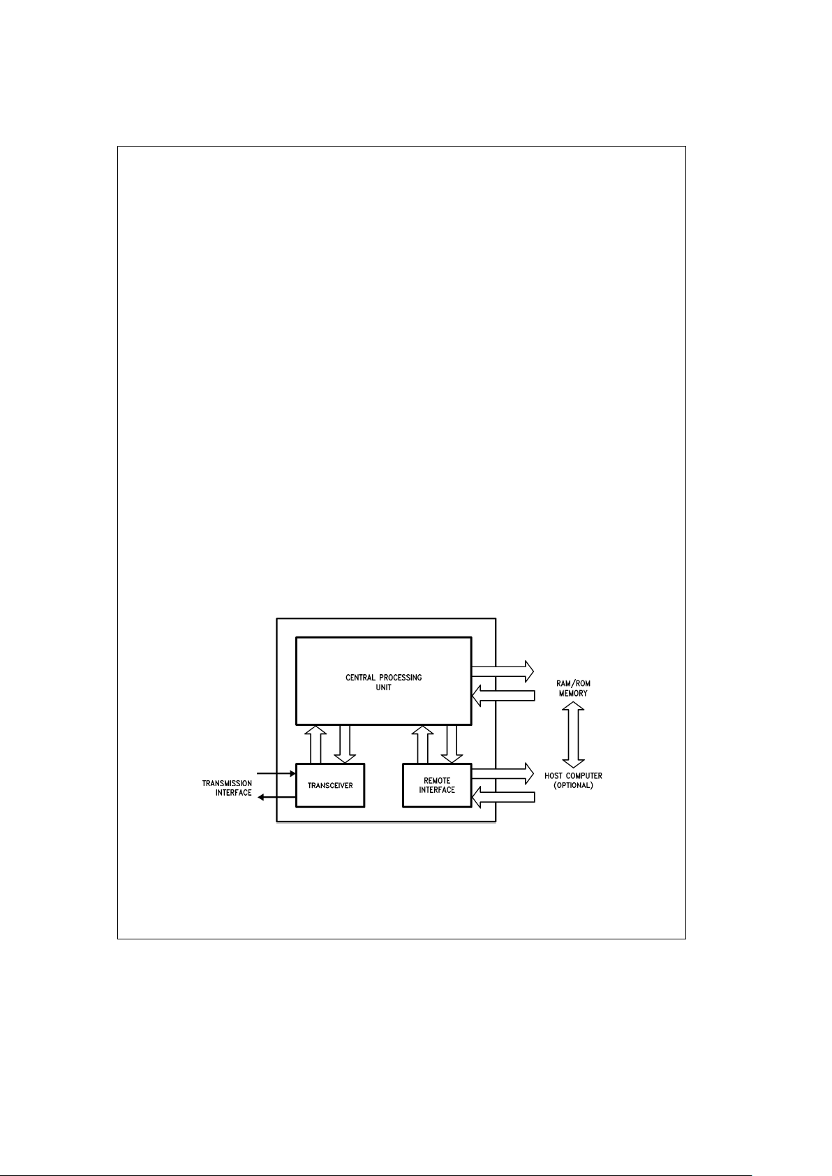
1.2 INTERNAL ARCHITECTURE INTRODUCTION
The DP8344B Biphase Communications Processor (BCP) is
divided into three major functional blocks: the Transceiver,
the Central Processing Unit (CPU), and the Remote Interface and Arbitration System, RIAS.
Figure 1-3
shows how
these blocks are related to each other and to other system
components.
The transceiver consists of an asynchronous transmitter
and receiver which can communicate across a serial data
path. The transmitter takes parallel data from the CPU and
appends to it the appropriate framing information. The resulting message is shifted out and is available as a serial
data stream on two output pins. The receiver shifts in serial
messages, strips off the framing information, and makes the
data available in parallel form to the CPU. The framing information supplied by the BCP provides the proper message
format for several popular communication protocols. These
include IBM 3270, 3299, and 5250, as well as a general
purpose 8-bit mode.
The transceiver clock may be derived from the internal oscillator, either directly or through internal divide-down circuitry. There is also an input for an external transceiver clock,
thus allowing complete flexibility in the choice of data rates.
The receiver input can come from three possible sources.
There is a built-in differential amplifier which is suitable for
most line interfaces, a single-ended digital input for use with
an external comparator, and an internal loopback path for
self testing. Refer to the Transceiver section for a detailed
description of all transmitter and receiver functions, and to
the application note on coax interfaces for the proper use of
the differential amplifier.
The CPU is a general purpose, 8-bit microprocessor capable of 20 MHz operation. It has a reduced instruction set
which is optimized for transceiver and data handling performance. It also has a full function arithmetic/logic unit
(ALU) which performs addition, subtraction, Boolean operations, rotations and shifts. Separate instruction and data
memory systems are supported, each with 16-bit address
buses, for a total of 64k address space in each.
There are 44 internal registers accessible to the CPU.
These include special configuration and control registers for
the transceiver and processor, four 16-bit indices to data
memory, and 20 8-bit general purpose registers. There is
also a 16-bit timer and a 16-byte deep LIFO data stack
which are accessible in the register address space. For
more detailed information, see the specific sections on the
Register set, the Timer, and the ALU.
The BCP can operate independently or with another processor as the host system. If such a system is required, communication with the BCP is possible by sharing data memory. The Remote Interface controls bus arbitration and access to data memory, as well as program up-loading and
execution. For example, it is possible for a host system to
load the BCP’s instruction memory and begin program execution, then pass data back and forth through data memory
accesses. The section on the Remote Interface and Arbitration System provides all of the necessary timing and control
information to implement an interface between a BCP and a
remote system.
As shown in
Figure 1-4,
the BCP uses two entirely separate
memory systems, one for program storage and the other for
data storage. This type of memory arrangement is referred
to as Harvard architecture. Each system has 16 address
lines, for a maximum of 64k words in each, and its own set
of data lines. The instruction (program) memory is two bytes
(16 bits) wide, and the data memory is one byte (8 bits)
wide.
In order to reduce the number of pins required for these
signals, the address and data lines for data memory are
multiplexed together. This requires an external latch and the
Address Latch Enable signal (ALE) for de-multiplexing.
TL/F/9336– B9
FIGURE 1-3. Simplified Block Diagram
9
Page 10
1.0 Communications Processor Introduction (Continued)
Simultaneous access to both data and program memory,
and instruction pipelining greatly enhance the speed performance of the BCP, making it well suited for real-time processing. The pipeline allows the next instruction to be retrieved from program memory while the current instruction is
being executed.
1.3 TIMING INTRODUCTION
The timing of all CPU operations, instruction execution and
memory access is related to the CPU clock. This clock is
usually generated by a crystal and the internal oscillator,
with optional divide by two circuitry. The period of the resulting CPU clock is referred to as a T-state; for example, a
20 MHz CPU clock yields a 50 ns T-state. Most CPU functions, such as arithmetic and logical operations, shifts and
rotates, and register moves, require only two T-states.
Branching instructions and data memory accesses require
three to four T-states.
Each memory system has a separate, programmable number of wait states to allow the use of slower memory devices. Instruction memory wait states are inserted into all instructions, as shown in
Figure 1-5,
thus they affect the
overall speed of program execution. Instruction memory
wait states can also apply when the Remote Interface is
loading a program into instruction memory. Data memory
wait states are only inserted into data memory access instructions, hence there is less degradation in overall program execution. Refer to the Timing section for detailed examples of all BCP instruction and data memory timing.
TL/F/9336– C1
FIGURE 1-4. Memory Configuration
TL/F/9336– C2
FIGURE 1-5. Effect of Memory Wait States on Timing
10
Page 11
1.0 Communications Processor Introduction (Continued)
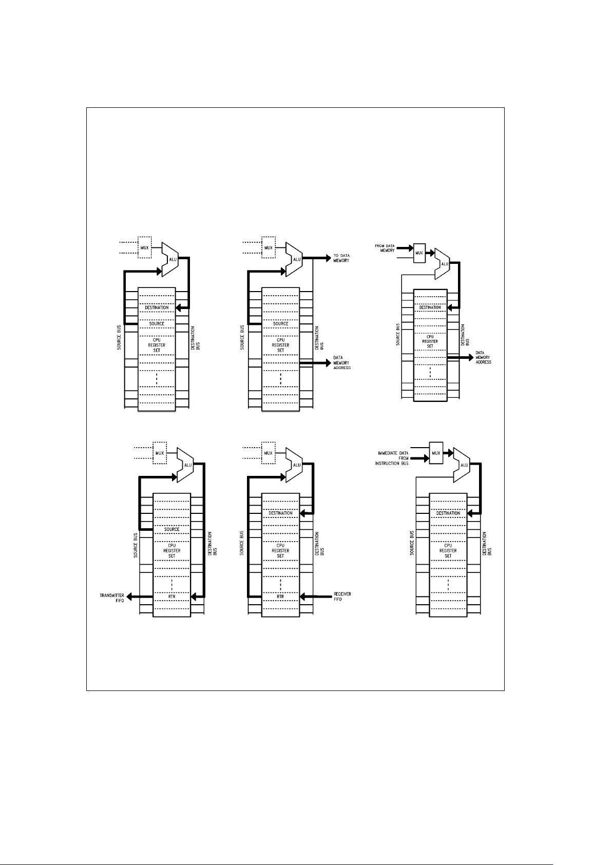
1.4 DATA FLOW
The CPU registers are all dual port, that is, they have separate input and output paths. This arrangement allows a single register to function as both a source and a destination
within the same instruction.
Figures 1-6a
through
1-6f
show the internal data flow path
for the BCP. The CPU registers are a central element to this
path. When a register functions as an output, its contents
are placed on the Source bus. When a register is an input,
data from the Destination bus is written into that register.
The other key element in the data path is the ALU. This unit
does all of the arithmetic and data manipulation operations,
but it also has bus multiplexing capabilities. Both the Data
Memory bus and a portion of the Instruction Memory bus
are routed to this unit and serve as alternative sources of
data. Since the data flow is always through this unit, most
data moves may include arithmetic manipulations with no
penalty in execution time.
Figure 1-6a
shows the data path for all arithmetic instructions and register to register moves. The source register
contents are placed on the Source bus, routed through the
TL/F/9336– C3 TL/F/9336– C4
TL/F/9336– C5
FIGURE 1-6a. Register to Register FIGURE 1-6b. Data Memory WRITE FIGURE 1-6c. Data Memory READ
TL/F/9336– C6 TL/F/9336– C7 TL/F/9336– C8
FIGURE 1-6d. WRITE to Transmitter FIGURE 1-6e. READ from Receiver FIGURE 1-6f. Load Immediate Data
11
Page 12
1.0 Communications Processor Introduction (Continued)
ALU/MUX, and then placed on the destination bus. This
data is then stored into the appropriate destination register.
Figures 1-6b
and
1-6c
show the data path for data memory
accesses. For a WRITE operation, the source register contents follow the same path through the ALU/MUX, but the
Destination bus is routed to output pins and on to data
memory. For a READ operation, incoming data is routed
onto the Destination bus by the ALU/MUX, and then stored
in a register. The address for all data memory accesses is
provided by one of four 16-bit index registers which can
operate in a variety of automatic increment and decrement
modes.
Transfer of the data byte between the CPU and the Transceiver is accomplished through a register location. This register,
À
RTRÓ, appears as a normal CPU register, but writing
to it automatically transfers data to the transmitter FIFO,
and reading from it retrieves data from the receiver FIFO.
These paths are illustrated in
Figures 1-6d
and
1-6e.
It is also possible to load immediate data into a CPU register. This data is supplied by the program and is usually a
constant such as a pointer or character. As shown in
Figure
1-6f,
a portion of the Instruction bus is routed through the
ALU/MUX for this purpose.
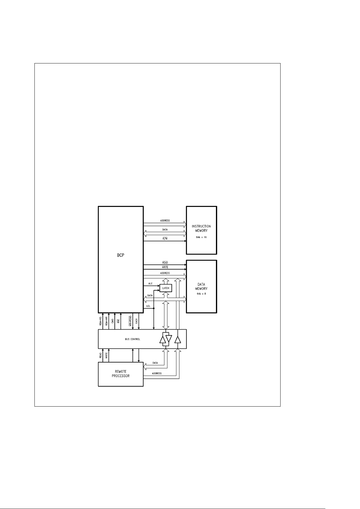
1.5 REMOTE INTERFACE AND ARBITRATION SYSTEM
INTRODUCTION
The BCP is designed to serve as a complete, stand alone
communications interface. Alternately, it can be interfaced
with another processor by means of the Remote Interface
and Arbitration System. Communication between the BCP
and the remote processor is possible by sharing data memory. Harvard architecture allows the remote system to access any BCP data memory location while the BCP continues to fetch and execute instructions, thereby minimizing
performance degradation.
Figure 1-7
shows a simplified remote processor interface.
This includes tri-state buffers on the address and data buses of the BCP’s Data Memory, and all of the control and
handshaking signals required to communicate between the
BCP and the host system.
There is an 8-bit control register, Remote Interface Control
À
RICÓ, accessible only to the remote system, which is used
to control a variety of features, including the types of memory accesses, interface speeds, single step program execution, CPU start/stop, instruction memory loads, and so forth.
Detailed information on all interface options is provided in
the section on Remote Interface and Arbitration System,
and in the related Reference section.
TL/F/9336– C9
FIGURE 1-7. Basic Remote Interface
12
Page 13
2.0 CPU Description
The CPU is a general purpose, 8-bit microprocessor capable of 20 MHz operation. It contains a large register set for
standard CPU operations and control of the transceiver.
The reduced instruction set is optimized for the communications environment. The following sections are an architectural and functional description of the DP8344B CPU.
2.1 CPU ARCHITECTURAL DESCRIPTION
2.1.1 Register Set
This section describes the BCP’s internal CPU registers. It is
a general overview of the register structure and the functions mapped into the CPU register space. It is not a detailed or exhaustive description of every bit. For such a description, please refer to Section 6.2, Register Set Reference. Also, the Remote Interface Configuration register,
À
RICÓ, is not accessible to the BCP (being accessible only
by the remote system) and is described in Section 6.3, Remote Interface Reference.
The register set of the BCP provides for a compliment of
both special function and general purpose registers. The
special function registers provide access to on-chip peripherals (transceiver, timer, interrupt control, etc.) while the
general purpose registers maximize CPU throughput by minimizing accesses to external data memory. The CPU can
address a total of 44 8-bit registers, providing access to:
#
20 general purpose registers
#
8 configuration and control registers
#
4 transceiver access registers
#
2 8-bit accumulators
#
4 16-bit pointers
#
16-bit timer
#
16 byte data stack
#
address and data stack pointers
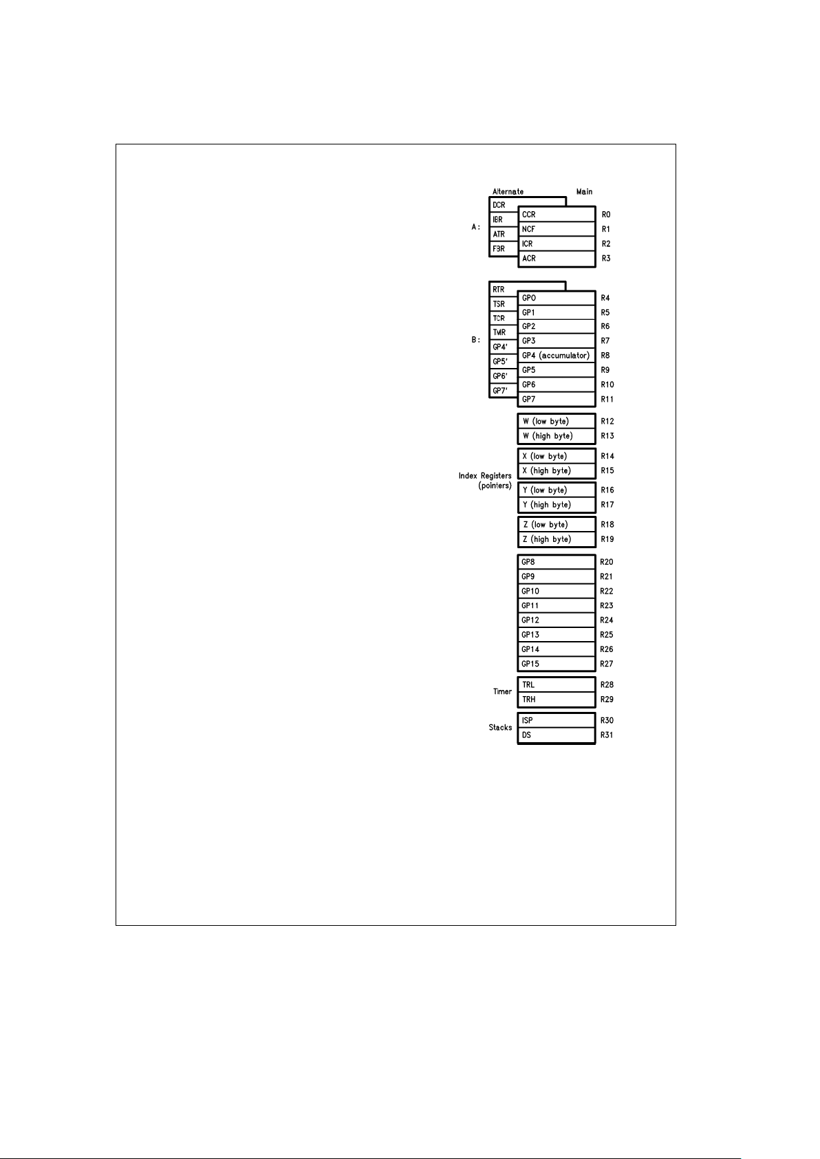
The CPU addresses internal registers with a 5-bit field, addressing 32 locations generically named R0 through R31.
The first twelve locations (R0 –R11) are further organized by
function as two groups of banked registers (A and B) as
shown in
Figure 2-1.
Each group contains both a main and
an alternate bank. Only one bank is active for group A and
one for bank B and thus accessible during program execution. Switching between the banks is performed by the exchange instruction EXX which selects whether Main A or
Alternate A occupies R0 – R3 and whether Main B or Alternate B occupies R4 –R11.
TL/F/9336– 32
FIGURE 2-1. Register Map
13
Page 14

2.0 CPU Description (Continued)
Registers in the R0– R11 address space are allocated in a
manner that minimizes the need to switch banks:
Main A: CPU control and transceiver status
Alternate A: CPU and transceiver configuration
Main B: 8 general purpose
Alternate B: 4 transceiver access, 4 general purpose
Most of the BCP’s instructions with register operand(s) can
access all 32 register locations. Only instructions with an
immediate operand are limited to the first sixteen register
locations (R0 – R15). These instructions, however, still have
access to all registers required for transceiver operation,
CPU status and control registers, 12 general purpose registers, and two of the index registers.
The general purpose registers are used for the majority of
BCP operations. There are 8 general purpose registers in
Main Bank B (R4 –R11), 4 in Alternate Bank B (R8 –R11),
and 8 more (R20–R27) that are always accessible but are
outside the limited register range. Since these registers are
internal to the BCP, they can be accessed without data
memory wait states, speeding up processing time. The index registers may also be used as general purpose registers
if required.
For those instructions that require two operands, an accumulator (R8, one in each bank) serves as the second operand. The result of such an operation is stored back in the
accumulator only if it is specified as the destination, thus
allowing three operand operations such as R5
a
R8xR20. See Section 2.1.3 Instruction Set for further explanation.
Most registers have a predetermined state following a reset
to the BCP. Refer to Section 6.2, Register Set Reference for
a detailed summary.
2.1.1.1 Banked Registers
The CPU register set was designed to optimize CPU performance in an environment which supports multiple tasks.
Generally the most important and time critical of these tasks
will be maintaining the serial link (servicing the transceiver
section) which often requires real time processing of commands and data. Therefore, all transceiver functions have
been mapped into special function registers which the CPU
can access quickly and easily. Switching between this task
and other tasks has been facilitated by dedicating a register
bank (Alternate B) to transceiver functions. Alternate Bank
B provides access to all transceiver status, control, and
data, in addition to four general purpose registers for protocol related storage. Main Bank B contains eight general purpose registers for use by other tasks. Having general purpose registers in both B banks allows for quick context
switching and also helps eliminate some of the overhead of
saving general purpose registers. The main objective of this
banked register structure is to expedite servicing of the
transceiver as a background (interrupt driven) task allowing
the CPU to efficiently interleave that function with other
background and foreground operations.
To facilitate using the transceiver in a polled fashion (instead of using interrupts), many of the status flags necessary to handshake with the transceiver are built into the
conditional jump instructions, with others available in the
Main A bank (normally active) so that Alternate Bank B does
not have to be switched in to poll the transceiver. Timer and
BIRQ tasks may also be run using polling techniques to
Main A bank.
In general, the registers have been arranged within the
banks so as to minimize the need to switch banks. The power-up state is Alternate bank A, Alternate bank B allowing
access to configuration registers. Again, the banks switch
by using the EXX instruction which explicitly specifies which
bank is active (Main or Alternate) for each register group (A
and B). The EXX instruction allows selecting any of four
possible bank settings with a single two T-state instruction.
This instruction also has the option of enabling or disabling
the maskable interrupts.
The contents of the special function registers can be divided into several groups for general discussionÐtiming/control, interrupt control, the transceiver, the condition codes,
the index registers, the timer, the stacks, and remote interface.
2.1.1.2 Timing/Control Registers
The BCP provides a means to configure its external timing
through setting bits in the Device Control Register,
À
DCRÓ,
and the Auxiliary Control Register,
À
ACRÓ. One of the first
configuration registers to be initialized on power-up/reset is
À
DCRÓwhich defines the hardware environment in which
the BCP is functioning. Specifically,
À
DCRÓcontrols the
clock select logic for both the CPU and transceiver, in addition to the number of wait states to be used for instruction
and data memory accesses.
The BCP allows either one clock source operation for the
CPU and the transceiver from the on-chip oscillator, or an
independent clock source can run the transceiver from the
eXternal Transceiver CLocK input, X-TCLK. The Transceiver Clock Select bits,[TCS1,0], select the clock source for
the transceiver which is either the on-chip Oscillator CLocK,
OCLK, or X-TCLK. Options for selecting divisions of the onchip oscillator frequency are also provided (see the description of
À
DCRÓin Section 6.2, Register Set Reference. The
CPU Clock Select bit,[CCS], allows the CPU to run at the
OCLK frequency or at half that speed. The clock output at
the pin CLK-OUT, however, is never divided and always reflects the crystal frequency OCLK. The frequency selected
for the transceiver (referred to as TCLK) should always be
eight times the desired serial data rate. The frequency selected for the CPU defines the length of each T-state (e.g.,
20 MHz implies 50 ns T-states).
There are two independent fields for defining wait states,
one for instruction memory access (n
IW
) and one for data
memory access (n
DW
). These fields specify to the BCP how
many wait states to insert to meet the access time requirements of both memory systems. The Instruction memory
Wait-state select bits,[IW1,0], and the Data memory Waitstate select bits,[DW2–0], control the number of inserted
wait states for instruction and data memory, respectively.
After a reset, the maximum number of wait states are set in
À
DCRÓ,n
IW
e
3 T-states and n
DW
e
7 T-states. Waitstates are discussed in more detail in Section 2.2.2, Timing.
For a complete discussion on choosing your memory and
determining the number of wait states required, please refer
to the application note
Choosing Your RAM for the Biphase
Communication Processor.
14
Page 15

2.0 CPU Description (Continued)
Another control bit in the
À
ACRÓregister is the Clock Out
Disable bit,[COD]. When[COD]is asserted, the buffered
clock output at pin CLK-OUT is tri-stated.
2.1.1.3 Interrupt Control Registers
The configuration bank (Alternate Bank A) includes an Interrupt Base Register,
À
IBRÓ, which defines the high byte of all
interrupt and trap vector addresses. Thus, the interrupt vector table can be located in any 256 byte page of the 64k
range of instruction addresses. The interrupt base is normally initialized once on reset before interrupts are enabled
or any traps are executed. Since NMI
is nonmaskable and
may occur before
À
IBRÓis initialized, the power-up/reset
value of
À
IBRÓ(00h) should be used to accommodate NMI
during initialization. In other words, if NMI is used in the
system, the absolute address 001Ch (the NMI
vector)
should contain a jump to an NMI
service routine.
The Interrupt Control Register,ÀICRÓ, provides individual
masks[IM4–0]for each of the maskable interrupts. The
Global Interrupt Enable bit,[GIE], located in
À
ACRÓworks
in conjunction with these individual masks to control each of
the maskable interrupts.
The external pin called BIRQ
is a Bidirectional Interrupt
ReQuest. BIRQ
is defined as an input or an output by the
Bidirectional Interrupt Control bit,[BIC],in
À
ACRÓ.[IM3
]
functions as BIRQ’s interrupt mask if BIRQ
is an input as
defines by[BIC]. When[BIC]defines BIRQ as an output,
[
IM3]controls the output state of BIRQ
.
Section 2.2.3, Interrupts provides a further description of
these registers.
2.1.1.4 Timer Registers
The timer block interfaces with the CPU via two registers,
TimeR Low byte,
À
TRLÓ, and TimeR High byte,ÀTRHÓ,
which form the input/output ports to the timer. Writing to
À
TRLÓandÀTRHÓstores the low and high byte, respectively, of a 16-bit time-out value into two holding registers. The
word stored in the holding registers is the value that the
timer will be loaded with via[TLD]. Also, the timer will automatically reload this word upon timing out. Reading
À
TRL
Ó
andÀTRHÓprovides access to the count down status of the
timer.
Control of timer operation is maintained via three bits in the
Auxiliary Control Register
À
ACRÓ. Timer STart[TST], bit 7
in
À
ACRÓ, is the start/stop control bit. Writing a one to
[
TST]allows the timer to start counting down from its current value. When low, the timer stops and the timer interrupt
is cleared. Timer Load[TLD],bit6in
À
ACRÓ, is the load
control of the timer. After writing the desired values into
À
TRLÓandÀTRHÓ, writing a one to[TLD]will load the 16-bit
word in the holding registers into the timer and initialize the
timer clock to zero in preparation to start counting. Upon
completing the load operation,[TLD]is automatically
cleared. Timer Clock Selection[TCS],bit5in
À
ACRÓ, determines the clock frequency of the timer count down. When
low, the timer divides the CPU clock by sixteen to form the
clock for the down counter. When[TCS]is high, the timer
divides the CPU clock by two. The input clock to the timer is
the CPU clock and should not be confused with the oscillator clock, OCLK. The rate of the CPU clock will be either
equal to OCLK or one-half of OCLK depending on the value
of bit 7 in the Device Control Register,
À
DCRÓ.
When the timer reaches a count of zero, the timer interrupt
is generated, the Time Out flag,[TO], (bit 7 in the Condition
Code Register
À
CCRÓ), goes high, and the timer reloads the
16-bit word stored in the holding registers to recycle through
a count down. The timer interrupt and[TO]can be cleared
by either writing a one to[TO]in
À
CCRÓor stopping the
timer by writing a zero to[TST]in
À
ACRÓ. Refer to Section
2.1.2, Timer for more information on the timer operation.
2.1.1.5 Transceiver Registers
Two registers in the Alternate A bank initialize transceiver
functions. The Auxiliary Transceiver Register,
À
ATRÓ, specifies a station address used by the address recognition logic
within the transceiver when using the non-promiscuous
5250 and 8-bit protocol modes. In 5250 modes,
À
ATRÓalso
defines how long the TX-ACT pin stays asserted after the
end of a transmitted message. The Fill Bit Register,
À
FBRÓ,
specifies the number of optional fill bits inserted between
frames in a multiframe 5250 message.
À
ICRÓcontains the Receiver Interrupt Select bits,[RIS1,0].
These bits determine the receiver interrupt source selection.
The source may be either Receiver FIFO Full, Data Available, or Receiver Active.
The Receive/Transmit Register,
À
RTRÓ, is the input/output
port to both the transmitter and receiver FIFO’s. It appears
to the BCP CPU like any other register. The
À
RTRÓregister
provides the least significant eight bits of data in both received and transmitted messages.
The Transceiver Mode Register,
À
TMRÓ, contains bits used
to set the configuration of the transceiver. As long as the
Transceiver RESet bit,[TRES], is high, the transceiver remains in reset. Internal LOOP-back operation of the transceiver can be selected by asserting[LOOP]. The RePeat
ENable bit,[RPEN], allows the receiver to be active at the
same time as the transmitter. When the Receiver INvert bit,
[
RIN], is set, all data sent to the receiver is inverted. The
Transmitter INvert bit,[TIN], is analogous to[RIN]except it
is for the transmitter. The protocol that the transceiver is
using is selected with the Protocol Select bits,[PS2–0].
The Transceiver Command Register,
À
TCRÓ, controls the
workings of the transmitter. To generate 5.5 line quiesce
pulses at the start of a transmission rather than 5, the Advance Transmitter Active bit,[ATA], must be set high. Parity
is automatically generated on a transmission and the Odd
Word Parity bit,[OWP], determines whether that parity is
even or odd. Bits 2– 0 of
À
TCRÓmake up part of the Trans-
mitter FIFO[TF10–8]along with
À
RTRÓ. Whenever a write
is made to
À
RTRÓ,[TF10–8]are automatically pushed on
the FIFO with the 8 bits written to
À
RTRÓ.
Other bits inÀTCRÓcontrol the operation of the on-chip
receiver. The number of line quiesce bits the receiver must
detect to recognize a valid message is determined by the
Receive Line Quiesce bit,[RLQ]. The BCP has its own internal analog comparator, but an off-chip one may be connected to DATA-IN. The receiver source is determined by the
Select Line Receiver bit,[SLR]. To view transceiver errors
in the Error Code Register,
À
ECRÓ, the Select Error Codes,
[
SEC], bit in
À
TCRÓmust be set high. When[SEC]is high,
Alternate Bank B R4 is remapped from
À
RTRÓtoÀECRÓso
that
À
ECRÓcan be read.
15
Page 16

2.0 CPU Description (Continued)
Just as[TF10–8]bits get pushed onto the transmitter FIFO
when a write to
À
RTRÓoccurs, the Receiver FIFO bits,
[
RF10–8], in the Transceiver Status Register,
À
TSRÓ, re-
flect the state of the top word of the receive FIFO.
À
TSR
Ó
also contains flags that show Transmit FIFO Full,[TFF],
Transmitter Active,[TA], Receiver Error,[RE], Receiver Active,[RA], and Data AVailable,[DAV]. These flags may be
polled to determine the state of the transceiver. For instance, during a Receiver Active interrupt, the BCP can query the[DAV]bit to determine whether data is ready in the
receiver FIFO yet.
The Error Code Register,
À
ECRÓ, contains flags for receiver
errors. As previously stated, the[SEC]bit in
À
TRCÓmust be
set high to read this register. Reading
À
ECRÓor resetting
the transceiver with[TRES]will clear all the errors that are
present. The receiver OVerFlow flag,[OVF], is set when the
receiver attempts to add another word to the FIFO when it is
full. If internally checked parity and parity transmitted with a
3270 message conflict, then the PARity error bit,[PAR],is
set high. The Invalid Ending Sequence bit,[IES],isset
when the ending sequence in a 3270, 3299, or 8-bit message is incorrect. When the expected mid-bit transition in
the Manchester waveform does not occur, a Loss of Mid-Bit
Transition occurs ([LMBT]). Finally, if the transmitter is activated while the receiver is active, the Receiver DISabled
while active flag,[RDIS], will be set unless[RPEN]is asserted.
The second register in Main A bank is called the Network
Command Flag register,
À
NCFÓ, and contains information
about the transceiver which is useful for polling the transceiver (during other tasks for example) to see if it needs
servicing. These flags include bits to indicate Transmit FIFO
Empty[TFE], Receive FIFO Full[RFF], Line Active[LA],
and a Line Turn Around[LTA].[LTA]indicates that a message has been received without error and a valid ending
sequence has occurred. These flags facilitate polling of the
transceiver section when transceiver interrupts are not
used. Also included in this register is a bit called[DEME
]
(Data Error/Message End). In 3270/3299 modes, this bit
indicates a mismatch between received and locally generated byte parity. In 5250 modes,[DEME]decodes an end of
message indicator (111 in the address field). Three other
bits: Received Auto Response[RAR], Acknowledge[ACK
]
and Poll[POLL]are decoded from a received message (at
the output of the receive FIFO) and are valid only in 3270/
3299 modes where response time is critical.
Section 3.0 Transceiver provides comprehensive coverage
of this on-chip peripheral.
2.1.1.6 Condition Codes/Remote Handshaking Register
The ALU condition codes are available in the Condition
Code Register
À
CCRÓ. The[Z]bit is set when a zero result
is generated by an arithmetic, logical, or shift instruction.
Similarly,[N]indicates the Negative result of the same operations. An oVerflow condition from an arithmetic instruction sets the[V]bit in
À
CCRÓ. The Carry bit[C]indicates a
carry or borrow result from an arithmetic instruction. See
Section 2.2.2, ALU for more information.
The Condition Code Register,
À
CCRÓ, also contains[BIRQ],
a status bit which reflects the logic level of the bidirectional
interrupt input pin BIRQ. Hence, this pin can be used as a
general purpose input/output port as well as a bidirectional
interrupt request as defined by bits in
À
ACRÓandÀICRÓ.Ifa
remote CPU is present and shares data memory (dual port
memory) with the BCP, handshaking can be accomplished
by using the two status bits in
À
CCRÓcalled[RR]and[RW],
which indicate Remote Read and Remote Write accesses,
respectively.
In
À
ACRÓ, a lock bit,[LOR], is available to lock out all host
accesses. When this bit is set, all host accesses are disabled. Locking out remote accesses is often done during
interrupts to ensure quick response times.
The Remote Interface Configuration register,
À
RICÓ,isnot
available to the BCP internally. The Remote Interface Reference section provides further detail on
À
RICÓand interfac-
ing a remote processor.
2.1.1.7 Index Registers
Four index registers called IW, IX, IY, and IZ provide 16-bit
addressing for both data memory and instruction memory.
Each of these index registers is actually a pair of 8-bit registers which are individually addressable just like any other
CPU register. They occupy register addresses R12 through
R19. Thus, the first two pointers IW and IX (comprising
R12–R15) can be accessed with immediate mode instructions (which can access only R0 to R15). Refer to Section
2.1.3.2, Addressing Modes to see how the index registers
are formed from R12 –R19.
Accessing data memory requires the use of one of the four
index registers. All such instructions allow you to specify
which pointer is to be used, except the immediate-relative
moves: MOVE rs,[IZ
a
n]and MOVE[IZan],rd. These instructions always use the IZ pointer. Register indirect operations have options to alter the value of the index register;
the options include pre-increment, post-increment, and
post-decrement. These options facilitate block moves,
searches, etc. Refer to Section 2.1.3, Instruction Set for
more information about data moves.
Since the BCP’s ALU is 8 bits wide, all code that manipulates the index registers must act on them eight bits at a
time.
The index registers can also be used in register indirect
jumps (LJMP[Ir]), useful in implementing relocatable code.
Any one of the index registers can be specified to provide
the 16-bit instruction address for the indirect jump.
2.1.1.8 Stack Registers
The last two register addresses (R30,R31) are dedicated to
provide access to the two on-chip stacksÐthe data stack
and the address stack. The data stack is 8 bits wide and 16
words deep. It is a Last In First Out (LIFO) type and provides
high speed storage for variables, pointers, etc. The address
stack is 23 bits wide and 12 words deep, providing twelve
levels of nesting of subroutines and interrupts. It is also a
LIFO structure and stores processor status as well as return
addresses from CALL instructions, TRAP instructions, and
interrupts. The seven bits of processor status consist of the
four ALU flags, ([C],[N],[V], and[Z]), the current bank
setting (two bits), and[GIE].
Stack pointers for both the on-chip stacks are provided in
R30, the Internal Stack Pointer register,
À
ISPÓ. The lower
four bits are the pointer for the data stack and the upper
four bits are the pointer for the address stack. Both internal
stacks are circular. For example if 16 bytes are written to
16
Page 17
2.0 CPU Description (Continued)
the data stack, the next byte pushed will overwrite the first.
À
ISPÓcan be read and written to like any other register, but
after a write, the BCP must execute one instruction before
reading the stack whose pointer was modified.
The Data Stack register,
ÀDSÓ
, is the input/output port for
the data stack. This port is accessed like any other register,
but a write to it will ‘‘push’’ a byte onto the stack and a read
from it will ‘‘pop’’ a byte from the stack. The data stack
pointer is updated when a read or write of
ÀDSÓ
occurs.
Information bits in the instruction address stack are not
mapped into the CPU’s register space and, therefore, are
not directly accessible. A remote system running a monitor
program can access this information by forcing the BCP to
single-step through a return instruction and then reading the
program counter. Since the stack pointers are writeable, the
remote system can access any location (return address) in
the address stack to trace program flow and then restore
the stack pointer to its original position.
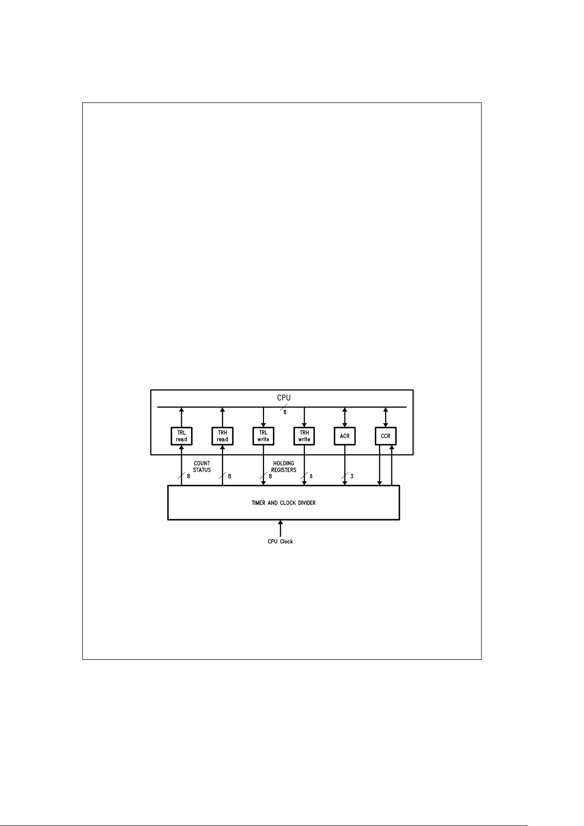
2.1.2 Timer
The BCP has an internal 16-bit timer that can be used in a
variety of ways. The timer counts independently of the CPU,
eliminating the waste of valuable processor bandwidth. The
timer can be used in a polled or interrupt driven configuration for user software flexibility.
The timer interfaces with the CPU via two registers, TimeR
Low byte,
À
TRLÓ, and TimeR High byte,ÀTRHÓ, which form
the input/output ports to the timer. Writing to
À
TRLÓand
À
TRHÓstores the low and high byte, respectively, of a 16-bit
time-out value into two holding registers. The word stored in
the holding registers is the value that the timer will be load-
ed with via[TLD]. Also, the timer will automatically reload
this word upon timing out. Reading
À
TRLÓandÀTRHÓpro-
vides access to the count down status of the timer.
Control of timer operation is maintained via three bits in the
Auxiliary Control Register
À
ACRÓ. Timer STart[TST], bit 7
in
À
ACRÓ, is the start/stop control bit. Writing a one to
[
TST]allows the timer to start counting down from its current value. When low, the timer stops and the timer interrupt
is cleared. Timer Load[TLD],bit6in
À
ACRÓ, is the load
control of the timer. After writing the desired values into
À
TRLÓandÀTRHÓ, writing a one to[TLD]will load the 16-bit
word in the holding registers into the timer and initialize the
timer clock to zero in preparation to start counting. Upon
completing the load operation,[TLD]is automatically
cleared. Timer Clock Selection[TCS],bit5in
À
ACRÓ, determines the clock frequency of the timer count down. When
low, the timer divides the CPU clock by sixteen to form the
clock for the down counter. When[TCS]is high, the timer
divides the CPU clock by two. The input clock to the timer is
the CPU clock and should not be confused with the oscillator clock, OCLK. The rate of the CPU clock will be either
equal to OCLK or one-half of OCLK depending on the value
of bit 7 in the Device Control Register,
À
DCRÓ.
When the timer reaches a count of zero, the timer interrupt
is generated, the Time Out flag,[TO], (bit 7 in the Condition
Code Register
À
CCRÓ), goes high, and the timer reloads the
16-bit word stored in the holding registers to recycle through
a count down. The timer interrupt and[TO]can be cleared
by either writing a one to[TO]in
À
CCRÓor stopping the
timer by writing a zero to[TST]in
À
ACRÓ. A block diagram
of the timer is shown in
Figure 2-2.
TL/F/9336– D1
FIGURE 2-2. Timer Block Diagram
17
Page 18

2.0 CPU Description (Continued)
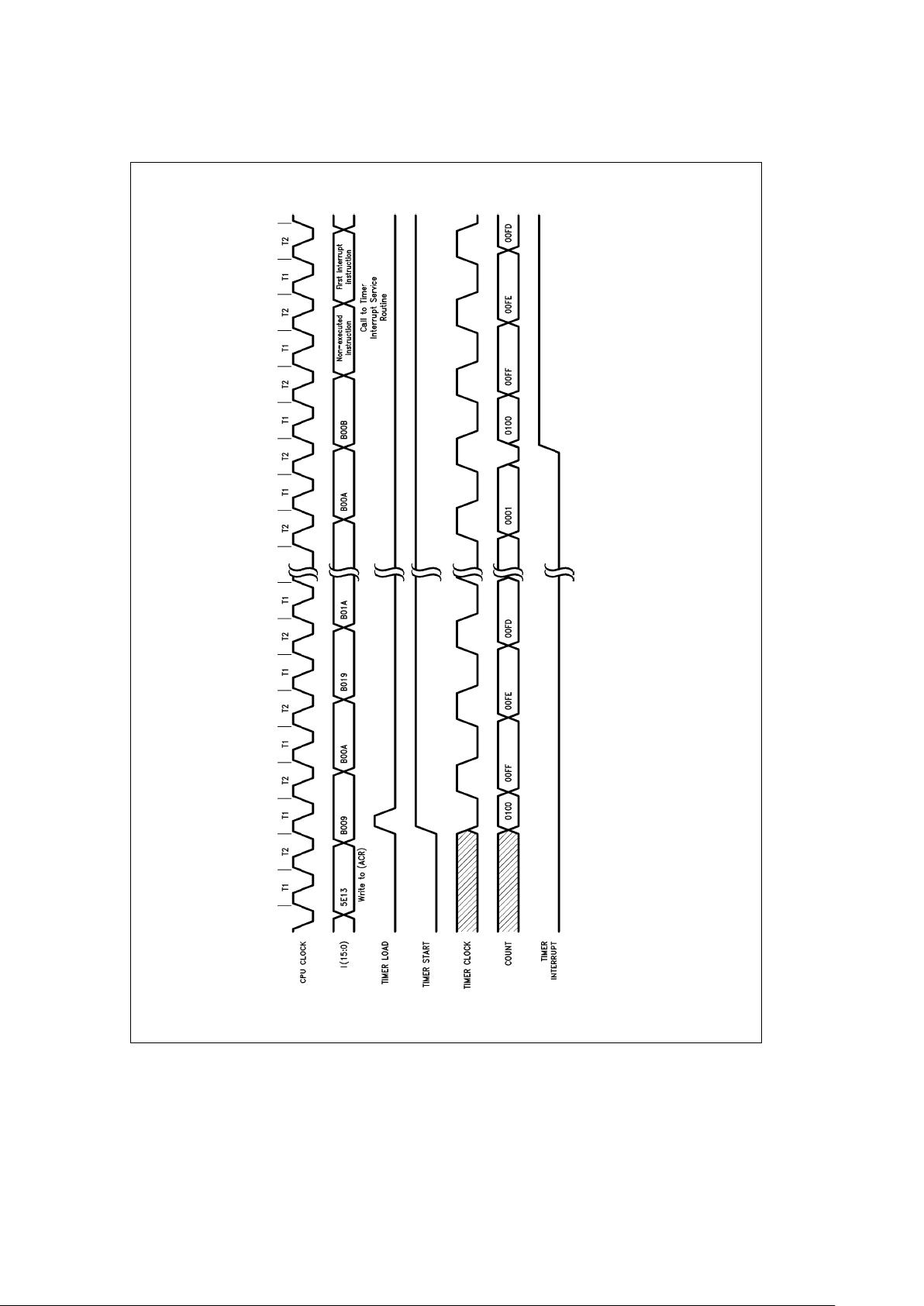
2.1.2.1 Timer Operation
After the desired 16-bit time-out value is written into
À
TRL
Ó
andÀTRHÓ, the start, load, and clock selection can be
achieved in a single write to
À
ACRÓ. A restriction exists on
changing the timer clock frequency in that[TCS]should not
be changed while the timer is running (i.e.,[TST]is high).
After a write to
À
ACRÓto load and start the timer, the timer
begins counting down at the selected frequency from the
value in
À
TRLÓandÀTRHÓ. Upon reaching a count of zero,
the timer interrupt is generated and, the timer reloads the
current word from
À
TRLÓandÀTRHÓto cycle through a
countdown again. The timing waveforms shown in
Figure
2-3
show a write toÀACRÓthat loads, starts, selects the
CPU clock rate/2 for the countdown rate, and asserts the
Global Interrupt Enable[GIE]. Prior to the write to
À
ACRÓ,
À
TRLÓandÀTRHÓwere loaded with 00h and 01h respectively, the timer interrupt was unmasked in the Interrupt
Control Register
À
ICRÓby clearing bit 4, and zero instruc-
tion wait states were selected in
À
DCRÓ. Since the write to
À
ACRÓasserted[GIE], the timer interrupt is enabled and
the CPU will vector to the timer interrupt service routine
address when the timer reaches a count of zero. The timer
interrupt is the lowest priority interrupt and is latched and
maintained until it is cleared in software. (See CPU Interrupts section). For very long time intervals, time-outs can be
accumulated under software control by writing a one to[TO
]
in
À
CCRÓallowing the timer to recycle its count down with
no other intervention. For time-outs attainable with one
count down, stopping the timer will clear the interrupt and
[TO]
. When the timer interrupt is enabled, the call to the
interrupt service routine occurs at different instruction
boundaries depending on when the timer interrupt occurs in
the instruction cycle. If the timer times out prior to T2, where
T2 is the last T-state of an instruction cycle, the call to the
interrupt service routine will occur in the next instruction.
When the time-out occurs in T2, the call to the interrupt
service routine will not occur in the next instruction. It occurs
in the second instruction following T2.
The count status of the timer can be monitored by reading
À
TRLÓand/orÀTRHÓ. When the registers are read, the output of the timer, not the value in the input holding registers,
is presented to the ALU. Some applications might require
monitoring the count status of the timer while it is counting
down. Since the timer can time-out between reads of
À
TRL
Ó
andÀTRHÓ, the software should take this fact into consideration. To read back what was written to
À
TRLÓandÀTRHÓ,
the timer must first be loaded via[TLD]without starting the
timer followed by a one instruction delay before reading
À
TRLÓandÀTRHÓto allow the output registers to be updat-
ed from the load operation.
To determine the time-out delay for a given value in
À
TRL
Ó
andÀTRHÓother than 0000h, the following equation can be
used:
TD
e
(value inÀTRHÓÀTRLÓ) * T * k
where:
ke2 when[TCS
]
e
1 or 16 when[TCS
]
e
0
TeThe period of the CPU clock
TD
e
The amount of time delay after the end of the in-
struction that asserts[TST]in
À
ACR
Ó
When the value of 0000h is loaded in the timer, the maximum time-out is obtained and is calculated as follows:
TD
e
65536 * T * k
With the CPU running full speed with an 18.8 MHz crystal,
the maximum single loop time delay attainable would be
55.6 ms ([TCS
]
e
0). The minimum time delay with the
same constraints is 106 ns ([TCS
]
e
1). For accumulating
time-out intervals, the total time delay is simply the number
of loops accumulated multiplied by the calculated time delay. The equations above do not account for any overhead
for processing the timer interrupt. The added overhead of
processing the interrupt may need to be included for precision timing.
18
Page 19
2.0 CPU Description (Continued)
TL/F/9336– D2
FIGURE 2-3. Timer Interrupt Diagram
19
Page 20
2.0 CPU Description (Continued)
2.1.3 Instruction Set
The followng paragraphs introduce the BCP’s architecture
by discussing addressing modes and briefly discussing the
Instruction Set. For detailed explanations and examples of
each instruction, refer to the Instruction Set Reference Section.
2.1.3.1 Harvard Architecture Implications
The BCP utilizes a true Harvard Architecture, where the instruction and data memory are organized into two independent memory banks, each with their own address and data
buses. Both the Instruction Address Bus and the Instruction
Bus are 16 bits wide with the Instruction Address Bus addressing memory by words. (A word of memory is 16 bits
long; i.e., 1 word
e
2 bytes.) Most of the instructions are
one word long. The exceptions are two words long, containing a word of instruction followed by a word of immediate
data. The combination of word sized instructions and a word
based instruction address bus eliminates the typical instruction alignment problems faced by many CPU’s.
The Data Address Bus is 16 bits wide (with the low order 8
bits multiplexed on the Data Bus), and the Data Bus is 8 bits
wide (i.e., one byte wide). The Data Address Bus addresses
memory by bytes. Most of the BCP’s instructions operate on
byte-sized operands.
Note that although both instruction addresses and data addresses are 16 bits long, these addresses are for two different buses and, therefore, have two different numerical
meanings, (i.e., byte address or word address.) Each instruction determines whether the meaning of a 16-bit address is that of an instruction word address or a data byte
address. Little confusion exists though because only the
program flow instructions interpret 16-bit addresses as instruction addresses.
2.1.3.2 Addressing Modes
An addressing mode is the mechanism by which an instruction accesses its operand(s). The BCP’s architecture supports five basic addressing modes: register, immediate, indexed, immediate-relative, and register-relative. The first
two allow instructions to execute the fastest because they
require no memory access beyond instruction fetch. The
remaining three addressing modes point to data or instruction memory. Typical of a RISC processor, most of the instructions only support the first three addressing modes,
with one of the operands always limited to the register addressing mode.
Register Addressing Modes
There are two terminologies for the register addressing
modes: Register and Limited Register. Instructions that allow Register operands can access all the registers in the
CPU. Note that only 32 of the 44 CPU registers are available
at any given point in time because the lower 12 register
locations (R0 –R11) access one of two switchable register
banks each. (See Section 2.1.1.1, Banked Registers for
more information on the CPU register banks.) Instructions
that allow the Limited Register operands can access just
the first 28 registers of the CPU. Again, note that only 16 of
these 28 registers are available at any given point in time.
Table 2-1 shows the notations used for the Register and
Limited Register operands. Some instructions also imply the
use of certain registers, for example the accumulators. This
is noted in the discussions of those instructions.
Immediate Addressing Modes
The two types of the immediate addressing modes available
are: Immediate numbers and Absolute numbers. Immediate
numbers are 8 bits of data, (one data byte), that code directly into the instruction word. Immediate numbers may represent data, data address displacements, or relative instruction addresses. Absolute numbers are 16-bit numbers. They
code into the second word of two word instructions and they
represent absolute instruction addresses. Table 2-2 shows
the notations used for both of these addressing modes.
TABLE 2-1. Register Addressing Mode Notations
Notation Type of Register Operand Registers Allowed
Rs Source Register R0–R31
Rd Destination Register R0–R31
Rsd Register is both a Source & Destination R0–R31
rs Limited Source Register R0–R15
rd Limited Destination Register R0–R15
rsd Limited Register is both a Source & Destination R0–R15
TABLE 2-2. Immediate Addressing Mode Notations
Notation Type of Immediate Operand Size
n Immediate Number 8 Bits
nn Absolute Number 16 Bits
20
Page 21
2.0 CPU Description (Continued)
Indexed Addressing Modes
Indexed operands involve one of four possible CPU register
pairs referred to as the index registers.
Figure 2-4
illustrates
how the index registers map into the CPU Register Set.
Note that the index registers are 16 bits wide.
Index registers allow for indirect memory addressing and
usually contain data memory addresses, although, the
LJMP instruction can use index registers to hold instruction
memory addresses. Most of the instructions that allow
memory indirect addressing, (i.e. the use of index registers),
also allow pre-incrementing, post-incrementing, or post-decrementing of the index register contents during instruction
execution, if desired. Table 2-3 lists the notations used for
the index register modes.
The index registers are set to zero when the BCP’s RESET
pin is asserted.
Index CPU Register Pair Forming Index Register
Register (MSB) (LSB)
IW R13 R12
15 8 7 0
IX R15 R14
15 8 7 0
IY R17 R16
15 8 7 0
IZ R19 R18
15 8 7 0
FIGURE 2-4. Index Register Map
Immediate-Relative and Register-Relative
Address Modes
The Immediate-Relative mode adds an unsigned 8-bit immediate number to the index register IZ forming a data byte
address. The Register-Relative mode adds the unsigned
8-bit value in the current accumulator, A, to any one of the
index registers forming a data byte address. Both of these
indirect memory addressing modes are available only on the
MOVE instruction. Table 2-4 shows the notation used for
these two addressing modes.
2.1.3.3 Instruction Set Overview
The BCP’s RISC instruction set contains seven categories
of instructions: Data Movement, Integer Arithmetic, Logic,
Shift-Rotate, Comparison, Program Flow, and Miscellaneous.
Data Movement Instructions
The MOVE instruction is responsible for all the data transfer
operations that the BCP can perform. Moving one byte at a
time, five different types of transfer are allowed: register to
register, data memory to register, register to data memory,
instruction memory to register, and instruction memory to
data memory. Table 2-5 lists all the variations of the MOVE
instruction.
TABLE 2-3. Index Register Addressing Mode Notations
Notation Meaning
[Ir]
Index Register, Contents Not Changed
[
Ir
b
]
Index Register, Contents Post-Decremented
[
Ir
a
]
Index Register, Contents Post-Incremented
[
a
Ir
]
Index Register, Contents Pre-Incremented
[
mIr
]
General Notation Indicating that Any of the Above Modes Is Allowed
Note:[]denotes indirect memory addressing and is part of the instruction syntax.
TABLE 2-4. Relative Index Register Mode Notations
Notation Type of Action Performed to Calculate a Data Memory Address
[
IZ
a
n
]
IZaImmediate Number (unsigned)xData Memory Address
[
Ir
a
A
]
Index RegisteraCurrent Accumulator (unsigned)xData Memory Address
Note:[]denotes indirect memory addressing and is part of the instruction syntax.
TABLE 2-5. Data Movement Instructions
Syntax Instruction Operation Addressing Modes
MOVE Rs, Rd registerxregister Register, Register
MOVE Rs,[mIr
]
register
x
data memory Register, Indexed
MOVE[mIr], Rd data memory
x
register Indexed, Register
MOVE Rs,[Ir
a
A
]
registerxdata memory Register, Register-Relative
MOVE[Ir
a
A], Rd data memoryxregister Register-Relative, Register
MOVE rs,[IZ
a
n
]
registerxdata memory Limited Register, Immediate-Relative
MOVE[IZ
a
n], rd data memoryxregister Immediate-Relative, Limited Register
MOVE n, rd instruction memoryxregister Immediate, Limited Register
MOVE n,[Ir
]
instruction memory
x
data memory Immediate, Indexed
21
Page 22

2.0 CPU Description (Continued)
Integer Arithmetic Instructions
The integer arithmetic instructions operate on 8-bit signed
(two’s complement) binary numbers. Two arithmetic functions are supported: Add and Subtract. Three versions of
the Add and Subtract instructions exist: operand
g
accumu-
lator, operand
g
accumulatorgcarry, and immediate oper-
and
g
operand. The first two versions support both the register and indexed addressing modes for the destination operand. These two versions also allow the specification of a
separate register or data address for the destination operand so that the sources may retain their integrity; (i.e., true
three-operand instructions). Note that the currently active
‘‘B’’ register bank selects which accumulator is used in
these instructions. The third version, immediate operand
g
operand, only supports the register addressing mode for the
destination operand with the register as both a source and
the destination. Table 2-6 lists the integer arithmetic instructions along with their variations.
Logic Instructions
The logic instructions operate on 8-bit binary data. A full set
of logic functions is supported by the BCP: AND, OR, eXclusive OR, and Complement. All the logic functions except
complement allow either an immediate operand or the currently active accumulator as an implied operand. Complement only allows one register operand which is both the
source and destination. The other logic instructions include
the following addressing modes: register, indexed, and immediate. As with the integer arithmetic instructions, the integrity of the sources may be maintained by specifying a
destination register which is different from the source. Table
2-7 lists all the logic instructions.
TABLE 2-6. Integer Arithmetic Instructions
Syntax Instruction Operation Addressing Modes
ADD n, rsd registeranxregister Immediate, Limited Register
ADDA Rs, Rd Rs
a
accumulatorxRd Register, Register
ADDA Rs,[mlr
]
Rs
a
accumulatorxdata memory Register, Indexed
ADCA Rs, Rd Rs
a
accumulatoracarryxRd Register, Register
ADCA Rs,[mlr
]
Rs
a
accumulatoracarryxdata memory Register, Indexed
SUB n, rsd register
b
nxregister Immediate, Limited Register
SUBA Rs, Rd RsbaccumulatorxRd Register, Register
SUBA Rs,[mlr
]
Rs
b
accumulatorxdata memory Register, Indexed
SBCA Rs, Rd Rs
b
accumulatorbcarryxRd Register, Register
SBCA Rs,[mlr
]
Rs
b
accumulatorbcarryxdata memory Register, Indexed
TABLE 2-7. Logic Instructions
Syntax Instruction Operation Addressing Modes
AND n, rsd register & nxregister Immediate, Limited Register
ANDA Rs, Rd Rs & accumulator
x
Rd Register, Register
ANDA Rs,[mlr
]
Rs & accumulator
x
data memory Register, Indexed
OR n, rsd register
l
nxregister Immediate, Limited Register
ORA Rs, Rd Rs
l
accumulatorxRd Register, Register
ORA Rs,[mlr
]
Rs
l
accumulatorxdata memory Register, Indexed
XOR n, rsd registerZnxregister Immediate, Limited Register
XORA Rs, Rd Rs
Z
accumulatorxRd Register, Register
XORA Rs,[mlr
]
Rs
Z
accumulatorxdata memory Register, Indexed
CPL Rsd register
x
register Register
Note: &elogical AND operation
l
e
logical OR operation
Z
e
logical exclusive OR operation
r
e
one’s complement
22
Page 23
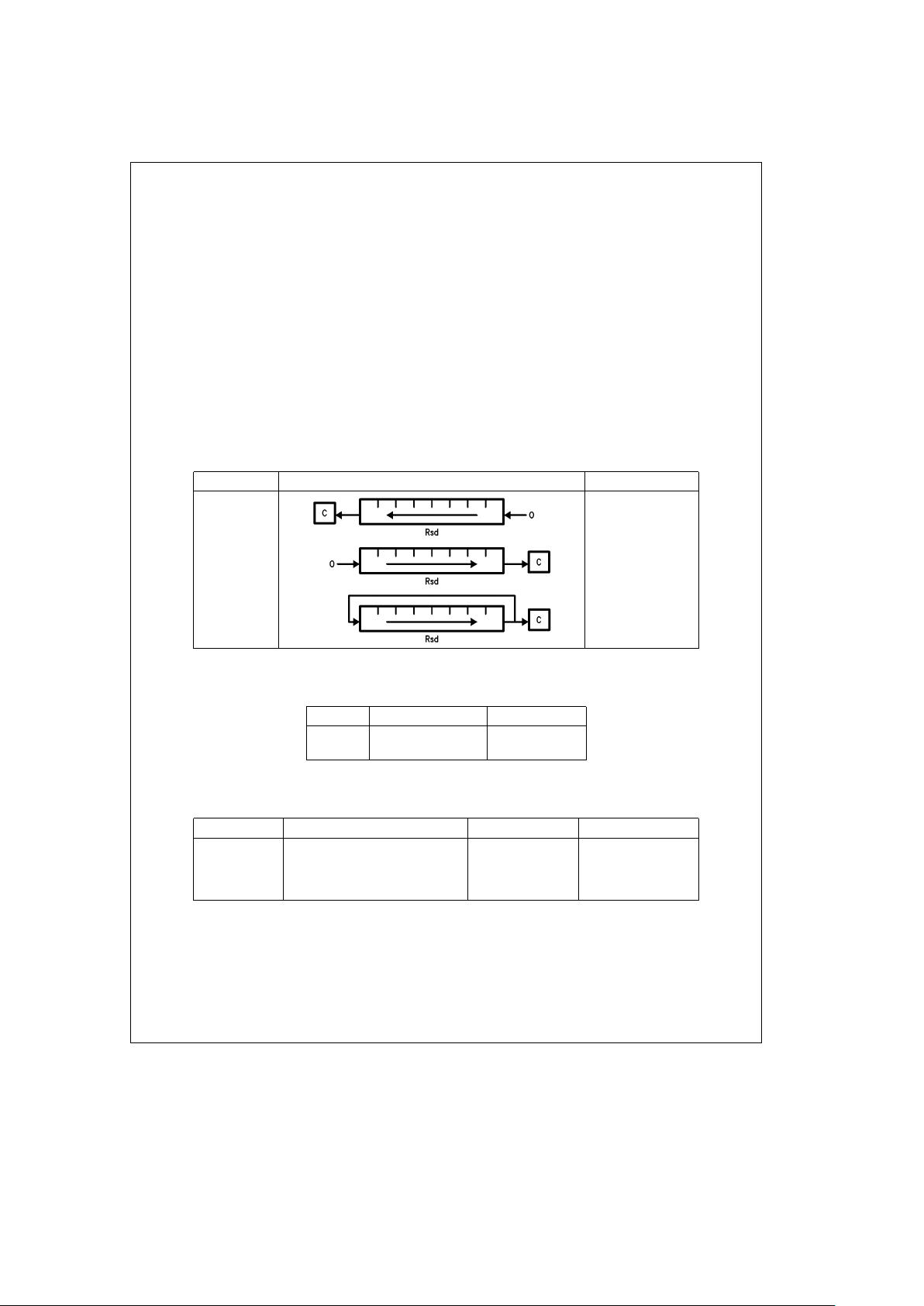
2.0 CPU Description (Continued)
Shift and Rotate Instructions
The shift and rotate instructions operate on any of the 8-bit
CPU registers. The BCP supports shift left, shift right, and
rotate operations. Table 2-8 lists the shift and rotate instructions.
Comparison Instructions
The BCP utilizes two comparison instructions. The CMP instruction performs a two’s complement subtraction between
a register and immediate data. The BIT instruction tests selected bits in a register by ANDing it with immediate data.
Neither instruction stores its results, only the ALU flags are
affected. Table 2-9 lists both of the comparison instructions.
Program Flow Instructions
The BCP has a wide array of program flow instructions: unconditional jumps, calls and returns; conditional jumps,
calls, and returns; relative or absolute instruction addressing
on jumps and calls; a specialized register field decoding
jump; and software interrupt capabilities. These instructions
redirect program flow by changing the Program Counter.
The unconditional jump instructions support both relative instruction addressing, the (JuMP instruction), and absolute
instruction addressing, (the Long JuMP instruction), using
the following addressing modes: Immediate, Register, Absolute, and Indexed. Table 2-10 lists the unconditional jump
instructions and their variations.
The conditional jump instructions support both relative instruction addressing and absolute instruction addressing using the Immediate and Absolute addressing modes. The
conditional relative jump instruction tests flags in the Condition Code Register,
À
CCRÓ, and the Transceiver Status
Register,
À
TSRÓ. Two possible syntaxes are supported for
the conditional relative jump instruction; see Table 2-11.
Table 2-12 lists the various flags ‘‘f’’ that the conditional
JMP instruction can test and Table 2-13 lists the various
conditions ‘‘cc’’ that the Jcc instruction can test for. Keep in
TABLE 2-8. Shift and Rotate Instructions
Syntax Instruction Operation Addressing Mode
SHL Rsd,b Register
SHR Rsd,b Register
ROT Rsd,b Register
Note: ‘‘b’’ethe number of bit shifts/rotates to perform.
TABLE 2-9. Comparison Instructions
Syntax Instruction Operation Addressing Mode
CMP rs, n registerbn Limited Register
BIT rs, n register & n Limited Register
Note: &elogical AND operation
TABLE 2-10. Unconditional Jump Instructions
Syntax Instruction Operation Operand Range Addressing Mode
JMP n PCan (sign extended)xPC
b
128,a127 Immediate
JMP Rs PC
a
Rs (sign extended)xPC
b
128,a127 Register
LJMP nn nn
x
PC 0, 64k Absolute
LJMP[Ir
]
Ir
x
PC 0, 64k Indexed
Note: PCeProgram Counter; contents initially points to instruction following jump.
23
Page 24

2.0 CPU Description (Continued)
mind that the Jcc instruction is just an optional syntax for
the conditional JMP instruction.
The example in
Figure 2-5
demonstrates two possible ways
to code the conditional relative jump instruction when testing for a false[Z]flag in
À
CCRÓ. In the example, assume
that the symbol ‘‘Z’’ equals ‘‘000’’ binary, that the symbol
‘‘NS’’ equals ‘‘0’’ binary, and that the symbol ‘‘SKIP.IT’’
points to the desired instruction with which to begin execution if[Z]is false.
On the other hand, the conditional absolute jump instruction, LJMP, can test any bit in any currently active CPU register. Table 2-14 shows the conditional long jump instruction
syntax.
JMP Z,NS,SKIP.IT ;If[Z]40 goto SKIP.IT
-or-
JNZ SKIP.IT ;If[Z]40 goto SKIP.IT
FIGURE 2-5. Coding Examples of Equivalent
Conditional Jump Instructions
TABLE 2-11. Conditional Relative Jump Instruction
Syntax Instruction Operation Operand Range Addressing Mode
JMP f,s,n If the flag ‘‘f’’ is in the state ‘‘s’’
b
128,a127 Immediate
then PC
a
n (sign extended)xPC
Jcc n If the condition ‘‘cc’’ is met
b
128,a127 Immediate
then PC
a
n (sign extended)xPC
Note: PCeProgram Counter; contents initially points to instruction following jump.
TABLE 2-12. ‘‘f’’ Flags
‘‘f’’(Binary) Flag Flag Name
Register
Containing Flag
000 Z Zero
À
CCR
Ó
001 C Carry
À
CCR
Ó
010 V Overflow
À
CCR
Ó
011 N Negative
À
CCR
Ó
100 RA Receiver Active
À
TSR
Ó
101 RE Receiver Error
À
TSR
Ó
110 DAV Data Available
À
TSR
Ó
111 TFF Transmitter FIFO Full
À
TSR
Ó
TABLE 2-13. ‘‘cc’’ Conditions Tested
‘‘cc’’ Field Condition Tested for Flag ‘‘f’’’s Condition
Z Zero
[Z]
e
1
NZ Not Zero
[Z]
e
0
EQ Equal
[Z]
e
1
NEQ Not Equal
[Z]
e
0
C Carry
[C]
e
1
NC No Carry
[C]
e
0
V Overflow
[V]
e
1
NV No Overflow
[V]
e
0
N Negative
[N]
e
1
P Positive
[N]
e
0
RA Receiver Active
[RA]
e
1
NRA Not Receiver Active
[RA]
e
0
RE Receiver Error
[RE]
e
1
NRE No Receiver Error
[RE]
e
0
DA Data Available
[
DAV
]
e
1
NDA No Data Available
[
DAV
]
e
0
TFF Transmitter FIFO FULL
[
TFF
]
e
1
NTFF Transmitter FIFO Not Full
[
TFF
]
e
0
TABLE 2-14. Conditional Absolute Jump Instruction
Syntax Instruction Operation Operand Range Addressing Mode
LJMP Rs,p,s,nn If the bit of register ‘‘Rs’’ in 0, 64k Register, Absolute
position ‘‘p’’ is in the state ‘‘s’’
then nn
x
PC
Note: PCeProgram Counter
24
Page 25

2.0 CPU Description (Continued)
The BCP also has a specialized relative jump instruction
called relative Jump with Rotate and Mask on source register, JRMK. This instruction facilitates the decoding of register fields often involved in communications processing.
JRMK does this by rotating and masking a copy of its register operand to form a signed program counter displacement
which usually points into a jump table. Table 2-15 shows the
syntax and operation of the JRMK instruction.
JRMK’s masking, (setting to zero), the least significant bit of
the displacement allows the construction of a jump table
using either one or two word instructions; for instance, a
table of JMP and/or LJMP instructions, respectively. The
example in
Figure 2-6
demonstrates the JRMK instruction
decoding the address frame of the 3299 Terminal Multiplex-
er protocol which is located in the Receive/Transmit Register,
À
RTR[4–2
]
Ó
.
The BCP has two unconditional call instructions; CALL,
which supports relative instruction addressing and LCALL,
(Long CALL), which supports absolute instruction addressing. These instructions push the following information onto
the CPU’s internal Address Stack: the address of the next
instruction; the status of the Global Interrupt Enable flag,
[
GIE]; the status of the ALU flags[Z],[C],[N], and[V]; and
the status of which register banks are currently active. Table
2-16 lists the two unconditional call instructions. Note that
the Address Stack is only twelve positions deep; therefore,
the BCP allows twelve levels of nested subroutine invocations, (this includes both interrupts and calls).
TABLE 2-15. JRMK Instruction
Syntax Instruction Operation
Displacement
Addressing Mode
Range
JRMK Rs, b, m (a) Rotate a copy of register ‘‘Rs’’ ‘‘b’’ bits to the right.
b
128,a126 Register
(b) Mask the most significant ‘‘m’’ bits and the least
significant bit of the above result.
(c) PC
a
resulting displacement (sign extended)xPC.
Note: PCeProgram Counter; contents initially points to instruction following jump.
Example Code
JRMK RTR,1,4 ;decode terminal address
LJMP ADDR.0 ;jump to device handler #0
LJMP ADDR.1 ;jump to device handler #1
...
LJMP ADDR.7 ;jump to device handler #7
Instruction Execution JRMK Displacement Register Contents
(a) Copy
À
RTRÓinto JRMK’s displacement register: x x x A2 A1 A0 y y
(b) Rotate displacement register 1 bit to the right: y x x x A2 A1 A0 y
(c) AND result with ‘‘00001110’’ binary mask: 0 0 0 0 A2 A1 A0 0
(d) Sign extend resulting displacement and add
it to the program counter, (PC).
If the bits A2 A1 A0 equal ‘‘0 0 1’’ binary then
a
2 is added to the Program Counter; 0 0 0 0 0 0 1 0
(i.e., PC
a
2xPC).
(e) Execute the instruction pointed to by the PC,
which in this example is:
LJMP ADDR.1
FIGURE 2-6. JRMK Instruction Example
TABLE 2-16. Unconditional Call Instructions
Syntax Instruction Operation
Operand
Addressing Mode
Range
CALL n PC &[GIE]& ALU flags & reg. bank selectionxAddress Stackb128,a127 Immediate
PC
a
n (sign extended)xPC
LCALL nn PC &[GIE]& ALU flags & reg. bank selection
x
Address Stack 0, 64k Absolute
nn
x
PC
Note: PCeProgram Counter; contents initially points to instruction following call.
[
GIE
]
e
Global Interrupt Enable bit.
&
e
concatenation operator, combines operands together forming one long operand.
25
Page 26

2.0 CPU Description (Continued)
The BCP has one conditional call instruction capable of
testing any bit in any currently active CPU register. This call
only supports absolute instruction addressing. Table 2-17
shows the conditional call instruction syntax and operation.
The return instruction complements the above call instructions. Two versions of the return instruction exist, the uncondtional return and the conditional return. When the unconditional return instruction is executed, it pops the last
address on the CPU’s Address Stack into the program
counter and it can optionally affect the[GIE]bit, the ALU
flags, and the register bank selection. Table 2-18 shows the
syntax and operation of the unconditional return instruction.
The conditional return instruction functions the same as the
unconditional return instruction if a desired condition is met.
As with the conditional jump instruction, the conditional return instruction has two possible syntaxes. Table 2-19 lists
the syntax for the conditional return. The ‘‘f’’ flags and the
‘‘cc’’ conditions for the return instruction are the same as
for the conditional jump instruction, therefore refer to Table
2-12 and Table 2-13 for the listing of ‘‘f’’ and ‘‘cc’’, respectively.
TABLE 2-17. Conditional Call Instruction
Syntax Instruction Operation Operand Range Addressing Mode
LCALL Rs, p, s, nn If the bit of register ‘‘Rs’’ in position 0, 64k Register, Absolute
‘‘p’’ is in the state ‘‘s’’ then
PC &[GIE]& ALU flags &
reg. bank selection
x
Address Stack
nn
x
PC
End if
Note: PCeProgram Counter; contents initially points to instruction following call.
[
GIE
]
e
Global Interrupt Enable bit
&
e
concatenation operator, combines operands together forming one long operand.
TABLE 2-18. Unconditional Return Instruction
Syntax Instruction Operation
RETÀgÀ,rfÓÓCase ‘‘g’’ of
0: leave[GIE]unaffected, (default)
1: restore[GIE]from Address Stack
2: set[GIE
]
3: clear[GIE
]
End case
If ‘‘rf’’e1 then
restore ALU flags from Address Stack
restore register bank selection from Address Stack
Else (the default)
leave the ALU flags and register bank selections unchanged
End if
Address Stack
x
PC
Note: PCeProgram Counter
[
GIE
]
e
Global Interrupt Enable bit
ÀÓ e
surrounds optional operands that are not part of the instruction syntax.
Optional operands may either be specified or omitted.
TABLE 2-19. Conditional Return Instruction
Syntax Instruction Operand
RETF f, sÀ,ÀgÓ,À,rf
ÓÓ
If the flag ‘‘f’’ is in the state ‘‘s’’ then perform a RETÀgÀ,rf
ÓÓ
Rcc
ÀgÀ
,rf
ÓÓ
If the condition ‘‘cc’’ is met then perform a RETÀgÀ,rf
ÓÓ
Note: See Table XVIII for an explanation of ‘‘RETÀgÀ,rfÓÓ’’
ÀÓ e
surrounds optional operands that are not part of the instruction syntax.
Optional operands may either be specified or omitted.
26
Page 27
2.0 CPU Description (Continued)
In addition to the above jump, call and return program flow
instructions, the BCP is capable of generating software interrupts via the TRAP instruction. This instruction generates
a call to any one of 64 possible interrupt table addresses
based on its vector number operand. This allows both the
simulation of hardware interrupts and the construction of
special software interrupts, if desired. The actual interrupt
table entry address is determined by concatenating the Interrupt Base Register,
À
IBRÓ, to an 8-bit representation of
the vector number operand in the TRAP instruction. This
instruction may also clear the[GIE]bit, if desired. Table
2-20 shows the syntax and operation of the TRAP instruction.
Miscellaneous Instructions
As stated in the ‘‘CPU Register Set’’ section, the BCP has
44 registers with 24 of them arranged into four register
banks: Main Bank A, Alternate Bank A, Main Bank B, and
Alternate Bank B. The exchange instruction, EXX, selects
which register banks are currently available to the CPU, for
example either Main Bank A or Alternate Bank A. The deselected register banks retain their current values. The EXX
instruction can also alter the state of[GIE], if desired. Table
2-21 shows the EXX instruction syntax and operation.
TABLE 2-20. TRAP Instruction
Syntax Instruction Operation Operand Range
TRAP vÀ,g
Ê
Ó
PC &[GIE]& ALU flags & 0, 63
reg. Bank Selection
x
Address Stack
If ‘‘g
Ê
’’e1 then clear[GIE
]
Form PC address as shown below:
Note: PCeProgram Counter; contents initially points to instruction following call.
[
GIE
]
e
Global Interrupt Enable bit
IBR
e
Interrupt Base Register
&
e
concatenation operator, combines operands together forming one long operand.
ÀÓe
surrounds optional operands that are not part of the instruction syntax.
Optional operands may either be specified or omitted.
TABLE 2-21. EXX Instruction
Syntax Instruction Operation
EXX ba, bbÀ,gÓCase ‘‘ba’’ of
0: activate Main Bank A
1: activate Alternate Bank A
End case
Case ‘‘bb’’ of
0: activate Main Bank B
1: activate Alternate Bank B
End case
Case ‘‘g’’ of
0: leave[GIE]unaffected, (default)
1: (reserved)
2: set[GIE
]
3: clear[GIE
]
End case
Note:[GIE
]
e
Global Interrupt Enable bit
ÀÓe
surrounds optional operands that are not part of the instruction syntax.
Optional operands may either be specified or omitted.
27
Page 28
2.0 CPU Description (Continued)
2.2 CPU FUNCTIONAL DESCRIPTION
2.2.1 ALU
The BCP provides a full function high speed 8-bit Arithmetic
Logic Unit (ALU) with full carry look ahead, signed arithmetic, and overflow decision capabilities. The ALU can perform
six arithmetic, nine logic, one rotate and two shift operations
on binary data. Full access is provided to all CPU registers
as both source and destination operands, and using the indirect addressing mode, results may be placed directly into
data memory. All operations which have an internal destination (register addressing) are completed in two (2) T-states.
External destination operations (indirect addressing to data
memory) complete in three (3) T-states.
Arithmetic operations include addition with or without carry,
and subtraction with or without borrow (represented by carry). Subtractions are performed using 2’s complement addition to accommodate signed operands. The subtrahend is
converted to its 2’s complement equivalent by the ALU and
then added to the minuend. The result is left in 2’s complement form.
The remaining ALU operations include full logic, shift and
rotate operations. The logic functions include Complement,
AND, OR, Exclusive-OR, Compare and Bit Test. Zero
through seven bit right and left shift operations are provided,
along with a zero through seven bit right rotate operation.
Note that the shift and rotate operations may only be performed on a register, which is both the source and destination. (See the Instruction Set Overview section for detailed
descriptions of these operations.)
The BCP ALU provides the programmer with four instruction
result status bits for conditional operations. These bits
(known as condition code flags) indicate the status (or condition) of the destination byte produced by certain instructions. Not all instructions have an affect on every status flag.
(See the Instruction Set Reference section for the specific
details on what status flags a given instruction affects.)
These flags are held in the Condition Code Register,
À
CCRÓ, see
Figure 2-7.
76543210
TO RR RW BIRQ N V C Z
where:
NeNegative
C
e
Carry
VeOverflow
ZeZero
FIGURE 2-7. Condition Code Register ALU Flags
If an instruction is documented as affecting a given flag,
then the flags are set (to 1) or cleared (to 0) under the
following conditions:
[N]
Ð The Negative flag is set if the most significant bit
(MSB) of the result is one (1), otherwise it is cleared.
This flag represents the sign of the result if it is interpreted as a 2’s complement number.
[C]
Ð The Carry flag is set if:
a) An addition operation generates a carry, see
Fig-
ure 2-8a.
b) A subtract or compare operation generates a bor-
row, see
Figure 2-8b.
c) The last bit shifted out during a shift operation (in
either direction) is a one (1), see
Figure 2-9.
d) The last bit rotated by the rotate operation is a one
(1), see
Figure 2-10.
In all other conditions[C]is cleared.
[V]
Ð Overflow is set whenever the result of an arithmetic or
compare operation on signed operands is not representable by the operand size, thereby producing an
incorrect result. For example, the addition of the two
signed negative numbers in
Figure 2-8a
would set[V
]
since the correct representation of the result, both
sign and magnitude, is not possible in 8 bits. On the
other hand, in
Figure 2-8b
and
2-8c
[V]
would be
cleared because the results are correctly represented
in both sign and magnitude. It is important to remember that Overflow is only meaningful in signed arithmetic and that it is the programmer’s responsibility to
determine if a given operation involves signed or unsigned values.
[Z]
Ð The Zero flag is set only when an operation produces
an all bits cleared result (i.e., a zero). In all other conditions[Z]is cleared.
11101010 10111010 11011100
a
10001100
b
11000100
a
01100011
1w01110110 1x11110110 1w00111111
[C]
e
1
[C]
e
1
[C]
e
1
[V]
e
1
[V]
e
0
[V]
e
0
(a) (b) (c)
FIGURE 2.8. Carry and Overflow Calculations
TL/F/9336– D3
FIGURE 2-9. Shifts’ Effect on Carry
TL/F/9336– D4
FIGURE 2-10. Rotate’s Effect on Carry
28
Page 29

2.0 CPU Description (Continued)
Several conditions apply to these flags, independent of their
operation and the way they are calculated. These conditions
are:
1. A flag’s previous state is retained when an instruction has
no affect on that flag.
2. Direct reading and writing of all ALU flags is possible via
the
À
CCRÓregister.
3. Currrent flag values are saved onto the address stack
during interrupt and call operations, and can be restored
to their original values if a return instruction with the restore flags option is executed.
4. Flag status is calculated in parallel with the instruction
result, therefore no time penalty is associated with flag
operation.
When performing single byte arithmetic (i.e., the values are
completely represented in one byte) the Add (ADD,ADDA)
and Subtract (SUB,SUBA) instructions should be used, but
when performing multi-byte arithmetic the Add with Carry
(ADCA) and Subtract with Carry (SBCA) instructions should
be used. This is because the carry (in an add operation) or
the borrow (in a subtract operation) must be carried forward
to the higher order bytes.
Figure 2-11
demonstrates an instruction sequence for a 16-bit add and an instruction sequence for a 16-bit subtract.
Assume the 16-bit variable X is represented by the register pair R4(MSB), R5(LSB), and that the 16-bit variable
Y is represented by the register pair R6(MSB), R7(LSB).
To perform the assignment Y
eXa
Y:
MOVE R7,A ;GET LSB OF Y
ADDA R5,R7 ;Y(LSB)4X(LSB)0Y(LSB)
MOVE R6,A ;GET MSB OF Y
ADCA R4,R6 ;Y(MSB)4X(MSB)0Y(MSB)
0CARRY
To perform the assignment YeX 1 Y:
MOVE R7,A ;GET LSB OF Y
SUBA R5,R7 ;Y(LSB)4X(LSB)1Y(LSB)
MOVE R6,A ;GET MSB OF Y
SBCA R4,R6 ;Y(MSB)4X(MSB)1Y(MSB)
1CARRY
FIGURE 2-11. Multi-Byte Arithmetic
Instruction Sequences
When using the ALU to perform comparisons, the programmer has two options. If the compare is to a constant value
then the CMP instruction can be used, else one of the subtract instructions must be used. When determining the results of any compare, the programmer must keep in mind
whether they are comparing signed or unsigned values. Table 2-22 lists the Boolean condition that must be met for
unsigned comparisons and Table 2-23 lists the Boolean
condition that must be met for signed comparisons.
TABLE 2-22
Unsigned Comparison Results
Comparison: xby Boolean Condition
xkyC
x
s
yC
l
Z
x
e
yZ
x
t
yC
x
l
yC&Z
Note: &elogical AND
l
e
logical OR
z
e
one’s complement
TABLE 2-23
Signed Comparison Results
Comparison: xby Boolean Condition
xky (N&V)l(N&V)
x
s
yZ
l
(N&V)l(N&V)
x
e
yZ
X
t
y (N&V)l(N&V)
xly (N&V&Z)l(N&V&Z)
Note: &elogical AND
l
e
logical OR
z
e
one’s complement
2.2.2 Timing
Timing on the BCP is controlled by an internal oscillator and
circuitry that generates the internal timing signals. This circuitry in the CPU is referred to as Timing Control. The internal timing of the CPU is synchronized to an internal clock
called the CPU clock, CPU-CLK. A period of CPU-CLK is
referred to as a T-state. The clock for the BCP is provided
by a crystal connected between X1 and X2 or from a clock
source connected to X1. This clock will be referred to as the
oscillator clock, OCLK. The frequency of OCLK is divided in
half when the CPU clock select bit,[CCS], in the Device
Control Register,
À
DCRÓ, is set to a one. Either OCLK or
OCLK/2 is used by Timing Control to generate CPU-CLK
and other synchronous signals used to control the CPU timing.
After the BCP is reset,[CCS]is high and CPU-CLK is generated from OCLK/2. Since the output of the divider that creates OCLK/2 can be high or low after reset, CPU-CLK can
also be in a high or low state. Therefore, the exact number
of clock cycles to the start of the first instruction cannot be
determined. Automatic test equipment can synchronize to
the BCP by asserting RESET
as shown in
Figure 2-12.
The
falling edge of RESET
generates a clear signal which causes CPU-CLK to fall. The next rising edge of X1 removes the
clear signal from CPU-CLK. The second rising edge of X1
will cause CPU-CLK to rise and the relationship between X1
and CPU-CLK can be determined from this point.
Writing a zero to[CCS]causes CPU-CLK to switch from
OCLK/2 to OCLK. The transition from OCLK to OCLK/2
occurs following the end of the instruction that writes to
29
Page 30
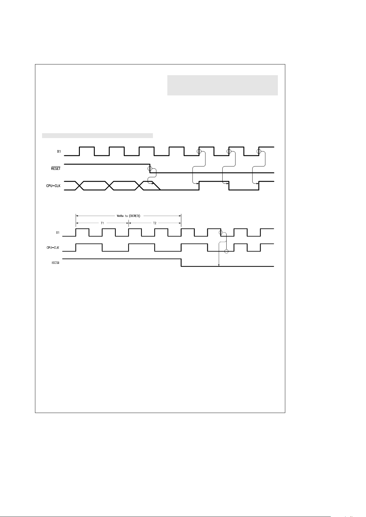
2.0 CPU Description (Continued)
[
CCS]as shown in
Figure 2-13.
The switch occurs on the
falling edge of X1 when CPU-CLK is low. CPU-CLK can be
changed back to OCLK/2 by writing a one to[CCS]. The
point at which CPU-CLK changes depends on whether
there has been an odd or even number of T-states since
[
CCS]was set low. The change would require a maximum
of two T-states and a minimum of one T-state following the
end of the instruction that writes to[CCS].
The CPU is a RISC processor with a limited number of instructions which execute in a short period of time. The maximum instruction cycle time is four T-states and the minimum
is two T-states. Six types of instruction timing are used in
the CPU: two T-state, three T-state program control, three
T-state data memory access, four T-state read data memory
access, four T-state program control, and four T-state two
word program control. The first T-state of each instruction
is T1 and the last T-state is T2. Intermediate T-states required to complete the instruction are referred to as TX.
The instruction clock output, ICLK, defines the instruction
boundaries. ICLK rises at the beginning of each instruction
and falls one-half T-state after the next address is generated on the instruction address bus, IA. Thus, ICLK indicates
the start of each instruction and when the next instruction
address is valid.
TL/F/9336– D5
FIGURE 2-12. CPU-CLK Synchronization with X1
TL/F/9336– D6
FIGURE 2-13. Changing from OCLK/2 to OCLK
30
Page 31

2.0 CPU Description (Continued)
Figure 2-14
shows the relationship between CPU-CLK,
ICLK, and IA for a two T-state instruction. The rising edge of
CPU-CLK generates ICLK at the start of T1. The next falling
edge of CPU-CLK increments the instruction address which
appears on IA. ICLK falls one-half T-state later. The instruction completes during T2 which ends with ICLK rising, signifying the beginning of the next instruction.
The three T-state program control instruction is similar and
is shown in
Figure 2-15.
An additional T-state, TX, is added
between T1 and T2. ICLK rises at the beginning of T1 as
before but falls at the end of TX. The next instruction address is generated one-half T-state before the end of TX
and the instruction ends with T2.
The three T-state data memory access instruction timing is
shown in
Figure 2-16.
Again, TX is inserted between T1 and
T2. ICLK rises at the beginning of the instruction and falls at
the end of T1. The next instruction address appears on IA
one-half clock cycle before ICLK falls. The address latch
enable output, ALE, rises halfway through T1 and falls half-
way through TX. The BCP has a 16-bit data memory address bus and an 8-bit data bus. The data bus is multiplexed
with the lower 8 bits of the address bus and ALE is used to
latch the lower 8 bits of the address during a data memory
access. The upper 8 bits of the address become valid onehalf T-state after the beginning of T1 and go invalid one-half
T-state after the end of T2. The lower 8 bits of the address
become valid on the address-data bus, AD, when ALE rises
and goes invalid one-half T-state after ALE falls.
Figure 2-16
shows a write to data memory in which case AD switches
from address to data at the beginning of T2. The data is
held valid until one-half T-state after the end of T2. The
write strobe, WRITE
, falls at the beginning of T2 and rises at
the end of T2. A read of data memory is shown in
Figure
2-17.
The read timing is the same as a write except one-half
T-state after ALE falls AD goes into a high impedance state
allowing data to enter the BCP from data memory. AD returns to an active state at the end of T2. The read strobe,
READ
, timing is identical to WRITE.
TL/F/9336– D7
FIGURE 2-14. Two T-state Instruction
TL/F/9336– D8
FIGURE 2-15. Three T-state Program Control Instruction
31
Page 32

2.0 CPU Description (Continued)
TL/F/9336– D9
FIGURE 2-16. Three T-state Data Memory Write Instruction
TL/F/9336– E1
FIGURE 2-17. Three T-state Data Memory Read Instruction[4TR
]
e
0
32
Page 33

2.0 CPU Description (Continued)
When the Four T-state Read mode is selected ([4TR
]
e
1),
a second TX state is inserted before T2 and the timing of
the read strobe, READ
, is changed such that READ falls
one-half T-state after the beginning of the second TX.
Fig-
ure 2-18
shows a Four T-state Read of data memory. The
extra half T-state before READ
falls allows more time for the
BCP to TRI-STATE the AD lines before the memory circuit
begins driving those lines.
The four T-state program control instruction timing is shown
in
Figure 2-19
. The instruction has two TX states inserted
between T1 and T2. ICLK rises at the beginning of T1 and
falls at the end of the second TX. The next instruction address becomes valid halfway through the second TX. The
four T-state two word program control instruction timing is
the same as two consecutive two T-state instructions and is
shown in
Figure 2-20.
This timing describes the minimum cycle time required by
each type of instruction. The BCP can be slowed down by
changing the number of wait states selected in the Device
Control Register,
À
DCRÓ. The BCP can be programmed for
up to three instruction memory wait states (instruction wait
states) and seven data memory wait states (data wait
states). Instruction wait states affect all instruction types
while data wait states affect only data memory access instructions. Bits three and four in
À
DCRÓcontrol the number
of instruction wait states and bits zero, one and two are
used to select the number of data wait states. The relationships between the control bits and the number of wait states
selected are shown in Table 2-24 and Table 2-25. The BCP
is configured with three instruction wait states and seven
data wait states, and[4TR]set to zero after reset. A write
to
À
DCR[4,3
]
Ó
to change the number of instruction wait
states takes effect on the following instruction if that instruction is a three T-state or four T-state program control instruction. For the other instruction types, the new number of
instruction wait states will take effect on the instruction fol-
TL/F/9336– H5
FIGURE 2-18. Four T-state Data Memory Read Instruction[4TR
]
e
1
33
Page 34

2.0 CPU Description (Continued)
TL/F/9336– E2
FIGURE 2-19. Four T-state Program Control Instruction
TL/F/9336– E3
FIGURE 2-20. Four T-state Two Word Instruction
TABLE 2-24. Data Memory
Wait States
À
DCR[2–0
]
Ó
Data Wait States
000 0
001 1
010 2
011 3
100 4
101 5
110 6
111 7
TABLE 2-25. Instruction Memory
Wait States
À
DCR[4,3
]
Ó
Instruction Wait States
00 0
01 1
10 2
11 3
34
Page 35

2.0 CPU Description (Continued)
lowing the instruction after the write to
À
DCRÓ. A write to
À
DCR[2–0
]
Ó
to change the number of data wait states will
take effect on the next data memory access instruction
even if it immediately follows the write to
À
DCRÓ.
A write to
À
DCR[2–0
]
Ó
to change the number of data wait
states or to
À
ACR[4TR
]
Ó
will take effect on the next data
memory access instruction even if it immediately follows
write to
À
DCRÓorÀACRÓ. Both instruction and data
wait states cause the insertion of additional T-states prior to
T2 and these T-states are referred to as TW. The purpose
of instruction wait states is to increase the time from instruction address generation to the beginning of the next instruction cycle. Data wait states increase the time from data
memory address generation to the removal of the strobe at
the end of data memory access instructions. Therefore, instruction and data wait states are counted concurrently in a
data memory access instruction and TX of a data memory
access instruction is counted as one instruction wait state.
The actual number of wait states added to a data memory
access is calculated as the maximum between the
number of data wait states and one less than the number of
instruction wait states.
Figure 2-21
shows a write of data
memory with one wait state. This could be accomplished by
selecting two instruction wait states or one data wait state.
The effect of the wait state is to increase the time the write
strobe is active and the data is valid on AD. The same situation for a read of data memory is shown in
Figure
2-22. Note that if[4TR]is set to one then one data wait
state has no additional affect on a read of data memory and
the timing is the same as shown in
Figure 2-18.
The affect of
two data memory wait states and[4TR]set to one is shown
in
Figure 2-23.
A two T-state instruction with two instruction
wait states is shown in
Figure 2-24
and a four T-state in-
struction with one instruction wait state is shown in
Figure
2-25.
As stated earlier, instruction wait states are inserted
before T2. Adding wait states to a four T-state two word
instruction causes the wait states to count twice when calculating total instruction cycle time. The wait states are added to each of the two words of the instruction.
TL/F/9336– E4
FIGURE 2-21. Data Memory Write with One Wait State
35
Page 36

2.0 CPU Description (Continued)
TL/F/9336– E5
FIGURE 2-22. Data Memory Read with One Wait State and[4TR
]
e
0
TL/F/9336– H6
FIGURE 2-23. Data Memory Read with Two Wait States and[4TR
]
e
1
36
Page 37

2.0 CPU Description (Continued)
TL/F/9336– E6
FIGURE 2-24. Two T-state Instruction with Two Wait States
TL/F/9336– E7
FIGURE 2-25. Four T-state Instruction with One Wait State
37
Page 38

2.0 CPU Description (Continued)
The WAIT
pin can also be used to add wait states to BCP
instruction execution. The CPU will be waited as long as
WAIT
is low. To wait a given instruction, WAIT must be asserted low one-half T-state prior to the beginning of T2 in
the instruction to be affected.
Figure 2-26
shows WAIT asserted during a write to data memory. In order to wait this
instruction, WAIT
must fall prior to the falling edge of CPUCLK in TX. One wait state is added to the access and WAIT
rises prior to the falling edge of CPU-CLK in TW which al-
lows the access to finish. If WAIT
had remained low, the
access would have been held off indefinitely. Programmed
wait states would delay when WAIT
must be asserted since
they would delay the beginning of T2.
Figures 2-27
through
Figure 2-29
depict the use of WAIT with three other instruc-
tion types. In all three cases, WAIT
is asserted one-half
T-state prior to when T2 would normally begin. Also, it is
evident that the effect of WAIT
on instruction timing is iden-
tical to adding programmed wait states.
TL/F/9336– E8
FIGURE 2-26. Data Memory Access WAIT Timing
TL/F/9336– E9
FIGURE 2-27. Two T-state Instruction WAIT Timing
38
Page 39

2.0 CPU Description (Continued)
TL/F/9336– F1
FIGURE 2-28. Three T-state Program Control Instruction WAIT Timing
TL/F/9336– F2
FIGURE 2-29. Four T-state Program Control Instruction WAIT Timing
LOCK
is another input which affects BCP instruction timing.
LOCK
prevents the BCP from accessing data memory.
When asserted low, LOCK
will cause the BCP to wait when
it executes a data memory access instruction. The BCP will
be waited until LOCK
is taken high. To prevent a given ac-
cess of data memory, LOCK
must be asserted low one-half
T-state prior to the beginning of the instruction accessing
data memory.
Figure 2-30
shows LOCK being used to wait a
write to data memory. LOCK
falls prior to the falling edge of
CPU-CLK before T1. In order to guarantee at least one wait
state, LOCK
is held low until after the falling edge of CPUCLK in T1. This causes the insertion of TW into the cycle
prior to TX. ALE remains high and the address is delayed on
AD until LOCK
is removed. After LOCK rises the access
concludes normally with ALE falling halfway through TX and
WRITE
occurring during T2. Note that LOCK waits the ac-
cess at a different point in the cycle than programmed wait
states or WAIT
. Additional wait states could occur from
these sources prior to T2.
Figure 2-31
shows an example of
LOCK
holding off a write to data memory with one pro-
grammed wait state.
With timing similar to LOCK
, the BCP will be delayed from
making a data memory access by an access from the remote system. If the remote system is accessing the Remote
Interface Configuration register,
À
RICÓ, or data memory, the
BCP will be waited by the Remote Interface and Arbitration
System, RIAS, until the remote access is finished. The
length of time the BCP is waited depends on the speed of
the remote system and the type of remote access. The wait
states are added prior to TX in the same manner as for
LOCK
shown in
Figure 2-30
. A more detailed description of
the operation of RIAS can be found in Section 4.0, Remote
Interface and Arbitration System.
39
Page 40

2.0 CPU Description (Continued)
TL/F/9336– F3
FIGURE 2-30. LOCK Timing
TL/F/9336– F4
FIGURE 2-31. LOCK Timing with One Wait State
40
Page 41

2.0 CPU Description (Continued)
The CPU will be stopped after RESET
is asserted low. The
CPU can be externally controlled by changing the state of
the start bit,[STRT],in
À
RICÓ. The CPU starts executing
instructions from the current address in the program control
register when a one is written to[STRT]and stops when
[
STRT]is cleared. The CPU will complete the current in-
struction before stopping. Controlling the CPU from
À
RIC
Ó
requires a processor to accessÀRICÓ. If no external processor is present, the CPU can be made to start automatically
after reset by holding REM-WR
and REM-RD low and RAE
high while RESET is transitioning from low to high. The CPU
‘‘kick-starts’’ and will begin executing instructions from address zero. The timing for kick-starting the CPU is shown in
Figure 2-32.
ICLK rises on the rising edge of CPU-CLK one
T-state after RESET
is de-asserted. The falling edge of
ICLK signifies the beginning of the first instruction fetch.
Three instruction wait states and T2 precede the first instruction.
A functional state diagram describing the timing of the CPU
is shown in
Figure 2-33.
The functional state diagram is similar to a flow chart, except that transitions to a new state
(states are denoted as rectangular boxes) can only occur on
the rising edge of the CPU-CLK. A state box can specify
several actions, and each action is separated by a horizontal line. A signal name listed in a state box indicates that that
pin will be asserted high when Timing Control has entered
that state. When the signal is omitted from a box, it is asserted low. (Note: this requires using the inversion of a signal in some cases.) Decision blocks are shown as diamonds
and their meaning is the same as in a flow chart. The functional state diagram is a generalized approach to determining instruction flow while allowing for any combination of
wait states and control signals. Timing Control always starts
from a reset in the state IDLE. After RESET
goes high, Timing Control remains in IDLE until[STRT]is written high. If
the BCP kick-starts, Timing Control enters TST on the next
rising edge of CPU-CLK. Timing Control starts with a dummy
instruction cycle in order to fetch the first instruction. ICLK
goes high in T1 and the instruction wait state counter is
loaded. ICLK falls when either T2 or TW is entered as determined by the value of i
IW
and WAIT. The normal instruction
flow begins after T2 at B on the diagram. As an example,
consider a three T-state data memory write instruction with
one data wait state. The instruction cycle path for this instruction would begin at T1 following the decision block for
data memory access. In T1, ICLK is asserted high, the instruction wait state counter is loaded, and a bus request to
RIAS is generated. Also, ALE is asserted high on the falling
edge of CPU-CLK during T1. A branch decision is now made
based on the state of LOCK
and the response from RIAS to
the bus request. Assuming that LOCK
is not asserted and a
remote access is not in progress, Timing Control enters TX
on the next rising edge of CPU-CLK. In TX, the data wait
state counter is loaded and the instruction wait state counter is decremented. In this example, the instruction wait
state counter is at zero and is not counting. The data wait
state counter is loaded with one. ALE goes low on the falling edge of CPU-CLK during TX. The next decision block
checks for a read of data memory. This example is a write to
data memory so the decision is no and the branch is to the
right. The wait state conditions are evaluated in the following decision block. i
DW
is one and Timing Control enters TW
on the next rising edge of CPU-CLK. WRITE
is asserted low
when TW is entered and the data wait state counter is decremented to zero. The decision on i
DW,iIW
, and WAIT is
now true and T2 is entered on the next rising edge of CPUCLK. WRITE
remains low. The CPU will stop execution if
[
STRT]is low at B in the diagram. Otherwise, the next instruction will be executed beginning at A. To summarize,
this instruction went through the following states: T1, TX,
TW, and T2. The complete instruction cycle is shown in
Fig-
ure 2-21.
Any instruction cycle can be analyzed in a similar
manner using this functional state diagram.
TL/F/9336– F5
FIGURE 2-32. CPU Start-Up Timing
41
Page 42

2.0 CPU Description (Continued)
TL/F/9336– F6
FIGURE 2-33. Functional State Diagram of CPU Timing
42
Page 43

2.0 CPU Description (Continued)
2.2.3 Interrupts
The DP8344B has two external and four internal interrupt
sources. The external interrupt sources are the Non-Maskable Interrupt pin, NMI
, and the Bi-directional Interrupt Re-
quest pin, BIRQ
.
External
A non-maskable interrupt is detected by the CPU when a
falling edge is detected at the NMI
pin. The interrupt is automatically cleared internally when the CPU recognizes the
interrupt.
BIRQ
can function as both an interrupt into the DP8344B
and as an output which can be used to interrupt other devices. BIRQ
is configured as an input or output according to
the state of[BIC]in the Auxiliary Control Register,
À
ACRÓ.
BIRQ
is an input if[BIC]is a zero and an output when[BIC
]
is a one. The reset state of[BIC]is a zero, causing BIRQ
to
be an input after the BCP is reset.[BIRQ]in the Condition
Code Register,
À
CCRÓ, is a read only bit which mirrors the
state of BIRQ
regardless of whether BIRQ is configured as
an input or output. This bit is updated at the beginning of T1
of each instruction.
When BIRQ
is configured as an input, an interrupt will occur
if the pin is held low. BIRQ
must be held low until the interrupt is recognized or the interrupt will not be processed. Due
to the prioritizing of interrupts as described below, BIRQ
may not be recognized by the CPU until higher priority interrupts have been serviced. BIRQ
will be recognized after
higher priority interrupts have been processed. The low
state on BIRQ
should be removed after the CPU recognizes
the interrupt or the interrupt will be processed multiple
times.
When BIRQ
is configured as an output, its state is controlled
by[IM3]in the Interrupt Control Register,
À
ICRÓ. Changing
the state of this bit will change BIRQ
at the beginning of T1
of the instruction following the write to[IM3]. Note that
[
BIRQ]in
À
CCRÓis also updated at the beginning of T1.
Therefore, there is a one instruction cycle delay from when
[
IM3]changes to when the new value of BIRQ
is made
available in[BIRQ].[BIS]in the Remote Interface Configuration register,
À
RICÓ, mirrors the state of[IM3]. When
BIRQ
is an output, writing a one to[BIS]will change the
state of[IME]thus changing BIRQ
and allowing a remote
processor to acknowledge an interrupt from the BCP. Note,
if the BCP code operates on[IM3]at the same time that the
remote processor acknowledges the interrupt by writing a
one to[BIS], BIRQ
will toggle and then assume the state of
[
IM3]resulting from the BCP code operation. Therefore, if
the designer chooses to operate on[IM3]while waiting for
the remote processor to acknowledge a BIRQ
interrupt, the
designer should ensure that the remote processor is locked
out from accessing[BIS]during the operation on[IM3].
This can be accomplished by setting[LOR]in
À
ACRÓ, having the BCP perform a data memory access to ensure that
any current remote accesses are complete, operating an
[
IM3], and finally clearing[LOR]. BIRQ
will change state
two T-states after the end of the write to[BIS]. Writing a
one to[BIS]will have no effect on[IM3]when BIRQ
is an
input. Table 2-26 summarizes the relationship between
BIRQ
and its associated register bits.
TABLE 2-26. BIRQ
Control Summary
(a) BIRQ
is an Input ([BIC
]
e
0): Remote Processor Controls the State of BIRQ
[
IM3
][
BIS
]
BIRQ
[
BIRQ
]
0[IM3
]
e
0 Active Interrupt to the BCP: state of Reflects the state of BIRQ
BIRQ controlled by the Remote
Processor
1[IM3
]
e
1 Masked Interrupt to the BCP: state of Reflects the state of BIRQ
BIRQ controlled by the Remote
Processor
(b) BIRQ is an Output ([BIC
]
e
1): BCP Controls the State of BIRQ
[
IM3
][
BIS
]
BIRQ
[
BIRQ
]
0[IM3
]
e
0 State of[IM3
]
e
0 Reflects the state of BIRQe0
1[IM3
]
e
1 State of[IM3
]
e
1 Reflects the state of BIRQe1
(c) BIRQ is an Output ([BIC
]
e
1): Remote Processor Acknowledges BIRQ
[
BIS
][
IM3
][
BIS
]
BIRQ
[
BIRQ
]
Remote Processor writesa1to[BIS
]
Toggles[IM3]State of[IM3]Reflects the
state of BIRQ
43
Page 44

2.0 CPU Description (Continued)
Internal
The internal interrupts consist of the Transmitter FIFO Empty, TFE, interrupt, the Line Turn Around, LTA, interrupt, the
Time Out, TO, interrupt, and a user selectable receiver interrupt source. The receiver interrupt source is selected from
either the Receiver FIFO, Full, RFF, interrupt, the Data
Available, DA, interrupt, or the Receiver Active, RA, interrupt. The receiver interrupt is selected using bits[RIS1]and
[
RIS0]in the Interrupt Control Register,
À
ICRÓ. See the
Section 3.0, Transceiver for a description of these interrupts.
Masking
The BCP uses two levels of interrupt masking: a global interrupt mask which affects all interrupts except NMI
and individual interrupt mask bits. Global enabling and disabling of
the interrupts is performed by changing the state of the
Global Interrupt Enable bit,[GIE],in
À
ACRÓ. The maskable
interrupts are disabled when[GIE]is a zero and enabled
when[GIE]is a one.[GIE]is a zero after the BCP is reset.
[
GIE]is a read/write register bit and may be changed by
using any instruction that can write to
À
ACRÓ. In addition,
the RET, RETF, and EXX instructions have option fields
which can be used to alter the state of[GIE]. The EXX
instruction can set or clear[GIE]as well as leaving it unchanged. The RET and RETF instructions can restore[GIE
]
to the value that was saved on the address stack at the time
the interrupt was recognized. These instructions also pro-
vide the options of clearing or setting[GIE]or leaving it
unchanged.[GIE]is set to a zero when an interrupt is recognized by the CPU. It is necessary to set[GIE]to a one if
interrupts are to be recognized within an interrupt routine.
The individual interrupt mask bits are located in
À
ICRÓ.
When set to a one, bits[IM0],[IM1],[IM2],[IM3], and[IM4
]
in
À
ICRÓmask the receiver interrupt, TFE interrupt, LTA in-
terrupt, BIRQ
interrupt, and TO interrupt, respectively. To
enable an interrupt, its mask bit must be set to a zero. The
interrupts and associated mask bits are shown in
Table 2-27. These bits are set to a one when the DP8344 is
reset.
Masking interrupts with[GIE]or the mask bits in
À
ICRÓprevents the CPU from acknowledging interrupts but does not
prevent the interrupts from occurring. Therefore, if an interrupt is asserted, it will be processed as soon as it is unmasked by changing[GIE]to a one and/or changing the
appropriate mask bit in
À
ICRÓto a zero.
Priorites
When more than one interrupt is unmasked and asserted,
the CPU processes the interrupt with the highest priority
first. NMI
has the highest priority followed by the receiver
interrupt, TFE, LTA, BIRQ
, and TO. Each time the interrupts
are sampled, the highest priority interrupt is processed first,
regardless of how long a lower priority interrupt has been
active. Interrupt priority is summarized in Table 2-27.
TABLE 2-27.
À
ICRÓInterrupt Mask Bits
and Interrupt Priority
Interrupt Mask Bit Priority
NMI Ð Highest
RFF, DA, RA
[
IMO
]
TFE
[
IM1
]
LTA
[
IM2
]
BIRQ
[
IM3
]
TO
[
IM4
]
Lowest
44
Page 45

2.0 CPU Description (Continued)
A call to the interrupt address is generated when an interrupt is detected by the CPU. The address for each interrupt
is constructed by concatenating the Interrupt Base Register,
À
IBRÓ, contents with the individual interrupt code as shown
in Table 2-28. There is room between the interrupt addresses for a maximum of four instruction words.
TABLE 2-28. Interrupt Vector Generation
Interrupt Code
NMI 111
RFF, DA, RA 001
TFE 010
LTA 011
BIRQ
100
TO 101
Interrupt Vector
À
IBRÓContents 0 0 0 Code 0 0
15 8 5 2 0
Interrupts are sampled by each falling edge of the CPU
clock with the last falling edge prior to the start of the next
instruction determining whether an interrupt will be processed. The timing of a typical interrupt event is shown in
Figure
2-34.
The interrupt occurs during the current instruction and
is sampled by the falling edge of the CPU clock. The next
instruction is not operated on and its address is stored in the
internal address stack along with[GIE], the ALU flags, and
the register bank positions. The address stack is twelve
words deep. A two T-state internal call is now executed in
place of the non-executed instruction. This call will cause a
branch to the interrupt address that is generated in the first
half of T-state T1. Also,[GIE]is cleared at the end of the
first half of T-state T1. The internal call to the interrupt address is subject to instruction wait states as configured in
À
DCRÓ.
2.2.4 Oscillator
The crystal oscillator is an on-chip amplifier which may be
used with an external crystal to generate accurate CPU and
transceiver clocks. The input to this amplifier is X1, pin 33.
The output of the amplifier is X2, pin 34. When X1 and X2
are connected to a crystal and external capacitors
(Figure
2-35),
the combined circuit forms a Pierce crystal oscillator
with the crystal operating at parallel resonance. Crystals
that oscillate over the frequency range of 2 MHz to 20 MHz
may be used. The recommended crystal parameters for operation with the oscillator are given in Table 2-29. The external capacitor values should be chosen to provide the manufacturer’s specified load capacitance for the crystal when
combined with the parasitic capacitance of the trace, socket, and package. As an example, a crystal with a specified
load capacitance of 20 pF used in a circuit with 13 pF per
pin parasitic capacitance will require external capacitor values of 27 pF each. This provides an equivalent capacitance
of 40 pF on each side of the crystal, and has a 20 pF series
equivalent value across the crystal.
As an alternative to the crystal oscillator, an external clock
source may be used. In this case, the external clock source
should be connected to X1 and no external circuitry should
be connected to X2
(Figure 2-36).
The DP8344 can supply a
clock source, equal in frequency to the crystal oscillator or
external clock source, to other circuitry via pin 35, the CLKOUT output. This output is a buffered version of the signal at
X1.
TABLE 2-29. Recommended Crystal Parameters
AT Cut, Parallel Resonant
Fundamental Mode
Load Capacitor
e
20 pF
Series Resistance
k
20X
Frequency Tolerance 0.005% at 25
§
C
Stability 0.01% 0
§
–70§C
Drive Level 0.5 mW Typical
TL/F/9336– F7
FIGURE 2-34. Interrupt Timing
45
Page 46

2.0 CPU Description (Continued)
TL/F/9336– F8
FIGURE 2-35. DP8344B Operation with Crystal
TL/F/9336– F9
FIGURE 2-36. DP8344B Operation with External Clock
3.0 Transceiver
3.1 TRANSCEIVER ARCHITECTURAL DESCRIPTION
The transceiver section operates as an on-chip, independent peripheral, implementing all the necessary formatting
required to support the physical layer of the following serial
communications protocols:
#
IBM 3270 (including 3299)
#
IBM 5250
#
NSC general purpose 8-bit
The CPU and transceiver are tightly coupled through the
CPU register space, with the transceiver appearing to the
CPU as a group of special function registers and three dedicated interrupts. The transceiver consists of separate transmitter and receiver logic sections, each capable of independent operation, communicating with the CPU via an asynchronous interface. This interface is software configurable
for both polled and interrupt-driven interaction, allowing the
system designer to optimize his product for the specific application.
The transceiver connects to the line through an external line
interface circuit which provides the required DC and AC
drive characteristics appropriate to the application. A block
diagram of such an interface is shown in
Figure 3-1.
An onchip differential analog comparator, optimized for use in a
transformer coupled coax interface, is provided at the input
to the receiver. Alternatively, if an external comparator is
necessary, the input signal may be routed to the DATA-IN
pin.
TL/F/9336– 33
FIGURE 3-1. System Block Diagram, Showing Details of the Line Interface
46
Page 47

3.0 Transceiver (Continued)
The transceiver has several modes of operation. It can be
configured for single line, half-duplex operation in which the
receiver is disabled while the transmitter is active. Alternatively, both receiver and transmitter can be active at the
same time for multi-channel (such as repeater) or loopback
operation. The transceiver has both internal and external
loopback capabilities, facilitating testing of both the software and external hardware. At all times, both transmitter
and receiver operate according to the same protocol definition.
3.1.1 Protocols
In all protocols, data is transmitted serially in discrete messages containing one or more frames, each representing a
single word of information. Biphase (Manchester II) encoding is used, in which the data stream is divided into discrete
time intervals (bit-times) denoted by a level transition in the
center of the bit-time. For the IBM 3270, 3299 and NSC
general purpose 8-bit protocols, a mid-bit transition from low
to high represents a biphase ‘‘1’’, and a mid-bit transition
from high to low represents a biphase ‘‘0’’. For the 5250
protocol, the definition of biphase logic levels is exactly reversed, i.e. a biphase ‘‘1’’ is represented by a high to low
transition. Depending on the bit sequence, there may or
may not be a transition on the bit-time boundary. The biphase encoding of a simple bit sequence is illustrated in
Figure 3-2(a)
.
Each transmission begins with a unique start sequence consisting of 5 biphase encoded ‘‘1’s’’, (referred to as ‘‘line
quiesce pulses’’) followed by a 3 bit-time code violation and
the sync bit of the first frame,
Figure 3-2(b)
. The three bittime code violation does not conform to the rules of Manchester encoding and forms a unique recognition pattern for
bit time synchronization by the receiver logic. The first bit of
any frame is the sync bit, a biphase ‘‘1’’. The frame is then
formatted according to the requirements of the protocol. If a
multi-frame message is being transmitted, additional frames
are appended to the end of the first frameÐexcept for the
5250 protocol, where there may be an optional number of
‘‘fill bits’’ (biphase ‘‘0’’) between each frame.
Depending on the protocol, when all data has been transmitted, the end of a message will be indicated either by the
transmission of an ending sequence, or (for 5250) simply by
the cessation of transitions on the differential line. Later
model 5250 equipment has incorporated a ‘‘line hold’’ at the
end of the message. The line hold maintains the final differential state on the line for several bit times to eliminate
noise or reflections that could be interpreted as a continuance of the message. The ending sequence for all but 5250
protocols consists of a single biphase ‘‘0’’ followed by a low
to high transition on the bit-time boundary and two bit-times
with no transitions (two mini-code violation),
Figure 3-2(c).
The various protocol framing formats are shown in
Figures
3-3
through
3-5
. The diagrams use a bit pattern drawing
convention which, for clarity, shows the bit-time boundaries
but not the biphase transitions in the center of the bit times.
The timing relationship between the biphase encoded bit
stream and the bit pattern diagrams is consistent with
Fig-
ure 3-2
.
TL/F/9336– 34
(a) Biphase Encoding
TL/F/9336– 36
(b) Starting Sequence
TL/F/9336– 35
(c) Ending Sequence
FIGURE 3-2. Biphase Encoding
3.1.1.1 IBM 3270
The framing format of the IBM 3270 coax protocol is shown
in
Figures 3-3(a)
and
(b)
, for both single and multi-frame
messages. Each message begins with a starting sequence
and ends with an ending sequence, as shown in
Figures
3-2(b)
and
(c)
. Each 12-bit frame begins with a sync bit (B1)
followed by an 8-bit data byte (MSB first), a 2-bit control
field, and the frame delimiter bit (B12), representing even
parity on the previous 11 bits. The bit rate on the coax line is
2.3587 MHz.
3.1.1.2 IBM 3299
Adding 3299 multiplexers to the 3270 environment requires
an address to be transmitted along with each message from
the controller to the multiplexer. The IBM 3299 Terminal
Multiplexer protocol provides this capability by defining an
additional 8-bit frame as the first frame of every message
sent from the controller, as shown in
Figure 3-3(c)
. This
frame contains a 6-bit data field along with the normal sync
and word parity bits. The protocol currently utilizes bits B2–
B4 as an address field that directs the message through the
multiplexor hardware. Following the address frame, the rest
of the message follows standard 3270 convention. The bit
rate, 2.3587 MHz, is the same as standard 3270.
3.1.1.3 IBM 5250
The framing format of the IBM 5250 twinax protocol is
shown in
Figure 3-4
, for both single and multi-frame messages. Each message begins with the starting sequence
shown in
Figure 3-2(b)
, and ends with 3 fill bits (biphase
‘‘0’’). A 16-bit frame is employed, consisting of a sync bit
(B15); an 8-bit data byte (B7– B14) (LSB first); a 3-bit station
address field (B4 –B6); and the last bit (B3) representing
47
Page 48

3.0 Transceiver (Continued)
TL/F/9336– 37
(a) 3270 Single-Byte Message
TL/F/9336– 38
(b) 3270 Multi-Byte Message
TL/F/9336– 39
(c) 3299 Controller/Multiplexer Message
FIGURE 3-3. 3270/3299 Protocol Framing Format
TL/F/9336– 40
(a) 5250 Single-Byte Message
TL/F/9336– 41
(b) 5250 Multi-Byte Message
FIGURE 3-4. 5250 Protocol Framing Format
48
Page 49

3.0 Transceiver (Continued)
even word parity on the previous 12 bits. Following the parity bit, 3 biphase ‘‘0’’ fill bits (B0–B2) are transmitted. Following these required fill bits, up to 240 additional fill bits can be
inserted between frames before the next sync bit and the
start of the next frame of a multi-byte message. The bit rate
on the twinax line is 1 MHz.
3.1.1.4 General Purpose 8-Bit
The framing format of the general purpose 8-bit protocol is
shown in
Figure 3-5
, for both single and multi-frame messages. It is identical to that used by the National Semiconductor DP8342 transmitter and DP8343 receiver chips.
Each message begins with a starting sequence and ends
with an ending sequence, as shown in
Figures 3-2(b)
and
(c)
. A 10-bit frame is employed, consisting of the sync bit
(B1); an 8-bit data byte (B2 –B9) (LSB first); and the last bit
of the frame (B10) representing even word parity on the
previous 9 bits. For multiplexed applications, the first frame
can be designated as an address frame, with all 8 bits available for the logical address. (See General Purpose 8-bit
Modes in this section.)
3.2 TRANSCEIVER FUNCTIONAL DESCRIPTION
A block diagram of the transceiver, revealing external inputs
and outputs and details of the CPU interface, is shown in
Figure 3-6
. The transmitter and receiver are largely independent of each other, sharing only the clock, reset and protocol select signals. The transceiver is mapped into the CPU
register space, thus the status of the transceiver can always
be polled. In addition, the CPU/Transceiver interface can be
configured for an interrupt-driven environment. (See Transceiver Interrupts in this section.)
Both transmitter and receiver are reset by a common Transceiver Reset bit,[TRES], allowing the CPU to independently
reset the transceiver at any time. The Transceiver is also
reset whenever the CPU reset is asserted, including the required power-up reset. When[TRES]is asserted, both
transmitter and receiver FIFO’s are emptied resulting in the
Transmit FIFO Empty flag[TFE]being asserted and the
Data Available flag[DAV]cleared. Other flags cleared by
[
TRES]are Transmit FIFO Full[TFF]and Transmitter Active[TA]in the transmitter and Line Active[LA], Receiver
Active[RA], Receiver Error[RE], Receive FIFO Full[RFF],
Data Error or Message End[DEME],[POLL],[ACK], and
[
RAR]command flags in the receiver. When[TRES]is asserted, external pin TX-ACT is cleared, DATA-DLY goes to a
state equal to the complement of Transmitter INvert[TIN]in
À
TMRÓ, and DATA-OUT goes into a state equal to the complement of[TIN]exclusive or’ed with the Advance Transmitter Active[ATA]in
À
TCRÓ. In other words, when[TRES]is
asserted, DATA-DLY
e
[
TIN], and DATA-OUT
e
[
TIN
] Z
[
ATA]. When[TRES]is asserted under software control, it
is necessary to wait at least one instruction after asserting
[
TRES]before seeing the resulting reset state of the affected flags in the CPU. The transmitter and receiver are
clocked by a common Transceiver Clock, TCLK, at a frequency equal to eight times the required serial data rate.
TCLK can either be obtained from the on-chip oscillator divided by 1, 2 or 4, or from an external clock applied to the
X-TCLK pin. TCLK selection is controlled by two Transceiver Clock Select bits,[TCS 1 – 0]located in the Device Control Register,
À
DCRÓ.[TCS 1 – 0]should only be changed
when the transceiver is inactive.
Since the TCLK source can be asynchronous with respect
to the CPU clock, the CPU/Transceiver interface can be
asynchronous. All flags from the Transceiver are therefore
latched at the start of all instructions, and parallel data is
transferred through 3 word FIFOs in both the transmitter
and receiver.
Protocol selection is controlled by three Protocol Select
bits,[PS2–0]in the Transceiver Mode Register,
À
TMR
Ó
(see Table 3-1). Enough flexibility is provided for the BCP to
operate in all required positions in the network. It is not pos-
TL/F/9336– 42
(a) 8-Bit Single-Byte Message
TL/F/9336– 43
(b) 8-Bit Multi-Byte Message
FIGURE 3-5. General Purpose 8-Bit Protocol Framing Format
49
Page 50

3.0 Transceiver (Continued)
sible for the transmitter and receiver to operate with different protocols at the same time. The protocol mode should
only be changed when both transmitter and receiver are
inactive.
If both transmitter and receiver are connected to the same
line, they should be configured to operate sequentially (halfduplex). This mode of operation is achieved by clearing the
RePeater ENable control bit[RPEN]in
À
TMRÓ. In this
mode, an active transmitter will disable the receiver, preventing simultaneous operation of transmitter and receiver.
If the transmitter FIFO is loaded while the receiver is actively processing an incoming signal, the receiver will be disabled and flag the CPU that a ‘‘Receiver Disabled While
Active’’ error has occurred. (See Receiver Errors in this sec-
tion.) On power-up/reset the transceiver defaults to this
half-duplex mode.
By asserting the Repeat Enable flag[RPEN], the receiver is
not disabled by the transmitter, allowing both transmitter
and receiver to be active at the same time. This feature
provides for the implementation of a repeater function or
loopback for test purposes.
The transmitter output can be connected to the receiver
input, implementing a local (on-chip) loopback, by asserting
[
LOOP].[RPEN]must also be asserted to enable both the
transmitter and receiver at the same time. With[LOOP]asserted, the output TX-ACT is disabled, keeping the external
line driver in TRI-STATE. The internal flag[TA]is still enabled, as are the serial data outputs.
TABLE 3-1. Protocol Mode Definition
PS2–0 Protocol Mode Comments
0 0 0 3270 Standard IBM 3270 protocol.
0 0 1 3299 Multiplexer Receiver expects first frame to be address frame. Transmitter uses standard
3270, no address frame.
0 1 0 3299 Controller Transmitter generates address frame as first frame. Receiver expects standard
3270, no address frame.
0 1 1 3299 Repeater Both transmitter and receiver operate with first frame as address frame.
1 0 0 5250 Non-promiscuous mode.[DAV]asserted only when first frame address matches
À
ATRÓ.
1 0 1 5250 Promiscuous
[
DAV]asserted on all valid received data without regard to address field.
1 1 0 8-Bit General-purpose 8-bit protocol with first frame address. Non-promiscuous mode.
[
DAV]asserted only when first frame address matches
À
ATRÓ.
1 1 1 8-Bit Promiscuous
[
DAV]asserted on all valid received frames.
50
Page 51

3.0 Transceiver (Continued)
TL/F/9336– 44
KEY TO REGISTERS
RTR Receive/Transmit Register ATR Auxiliary Transceiver Register
TSR Transceiver Status Register NCF Network Command Register
TCR Transceiver Command Register FBR Fill-Bit Register
TMR Transceiver Mode Register DCR Device Control Register
FIGURE 3-6. Block Diagram of Transceiver, Showing CPU Interface
51
Page 52

3.0 Transceiver (Continued)
3.2.1 Transmitter
The transmitter accepts parallel data from the CPU, formats
it according to the desired protocol and transmits it as a
serial biphase-encoded bit stream. A block diagram of the
transmitter logic is shown in
Figure 3-6
. Two biphase out-
puts, DATA-OUT
, DATA-DLY, and the external line driver
enable, TX-ACT, provide the data and control signals for the
external line interface circuitry. The two biphase outputs are
valid only when TX-ACT is asserted (high) and provide the
necessary phase relationship to generate the ‘‘predistortion’’ waveform common to all of the transceiver protocols.
See
Figure 3-7
for the timing relationships of these outputs
as well as the output of the line driver. For a recommended
3270/3299 coax interface, see Section 3.2.5.1 3270 Line
Interface. For a recommended 5250 twinax interface see
Section 3.2.5.2 5250 Line Interface.
The capability is provided to invert DATA-OUT
and DATADLY via the Transmitter Invert bit,[TIN], located in the
Transceiver Mode Register,
À
TMRÓ. In addition, the timing
relationship between TX-ACT and the two biphase outputs
can be modified with the Advance Transmitter Active control,[ATA]. When[ATA]is cleared low (the power-up condition), the transmitter generates exactly five line quiesce bits
at the start of each message, as shown in
Figure 3-7
.If
[
ATA]is asserted high, the transmitter generates a sixth line
quiesce bit, adding one biphase bit time to the start sequence transmission. The line driver enable, TX-ACT, is asserted halfway through this bit time, allowing an additional
half-bit to precede the first full line quiesce of the transmitted waveform. Also, the state of DATA-DLY is such that no
predistortion results on the line during this first half line
quiesce. This modified start sequence is depicted in the dotted lines shown in
Figure 3-7
and is used to limit the initial
transient voltage amplitude when the message begins.
Data is loaded into the transmitter by writing to the Receive/
Transmit Register
À
RTRÓ, causing the first location of the
FIFO to be loaded with a 12-bit word (8 bits from
À
RTRÓand
4 bits from the Transceiver Command Register
À
TCRÓ. The
data byte to be transmitted is loaded into
À
RTRÓ, and
À
TCRÓcontains additional information required by the pro-
tocol. It is important to note that if
À
TCRÓis to be changed,
it must be loaded before
À
RTRÓ. A multi-frame transmission
is accomplished by sequentially loading the FIFO with the
required data, the transmitter taking care of all necessary
frame formatting.
If the FIFO was previously empty, indicated by the Transmit
FIFO Empty flag[TFE]being asserted, the first word loaded
into the FIFO will asynchronously propagate to the last location in approximately 40 ns, leaving the first two locations
empty. It is therefore possible to load up the FIFO with three
sequential instructions, at which time the Transmit FIFO Full
flag[TFF]will be asserted. If
À
RTRÓis written while[TFF]is
high, the first location of the FIFO will be over-written and
that data will be destroyed.
When the first word is loaded into the FIFO, the transmitter
starts up from idle, asserting TX-ACT and the Transmitter
Active flag[TA], and begins generating the start sequence.
After a delay of approximately 16 TCLK cycles (2 biphase
bit times), the word in the last location of the FIFO is loaded
into the encoder and prepared for transmission. If the FIFO
was full,[TFF]will be de-asserted when the encoder is
loaded, allowing an additional word to be loaded into the
FIFO.
When the last word in the FIFO has been loaded into the
encoder,[TFE]goes high, indicating that the FIFO is empty.
To ensure the continuation of a multi-frame message, more
data must then be loaded into the FIFO before the encoder
starts the transmission of the last bit of the current frame
(the frame parity bit for 3270, 3299, and 8-bit modes; the
last of the three mandatory fill bits for 5250). This maximum
load time from[TFE]can be calculated by subtracting two
from the number of bits in each frame of the respective
protocol, and multiplying that result by the bit rate. This
number represents the best case time to loadÐthe worst
case value is dependent on CPU performance. Since the
CPU samples the transceiver flags and interrupts at instruction boundaries, the CPU clock rate, wait states (from programmed wait states, asserting the WAIT pin, or remote access cycles), and the type of instruction currently being executed can affect when the flag or interrupt is first presented
to the CPU.
If there is no further data to transmit (or if the load window is
missed), the ending sequence (3270/3299/8-bit) is generated and the transmitter returns to idle, de-asserting TX-ACT
and[TA]. In 5250 mode, the three required fill bits are sent
and TX-ACT and[TA]are de-asserted at a time dependent
on the value of bits 7 through 3 of the Auxiliary Transceiver
Register
À
ATRÓ.IfÀATR[7–3
]
Óe
00000, TX-ACT and[TA
]
are de-asserted at the end of the third required fill bit resulting in no additional ‘‘line hold’’ at the end of the message.
Each increment of
À
ATR[7–3
]
Ó
results in an additional half
bit time of line hold up to a maximum of 15.5 bit times.
Data should not be loaded into the FIFO after the transmitter is committed to ending the message and before the[TA
]
flag is deasserted. If this occurs, the load will be missed by
the transmitter control logic and the word(s) will remain in
the FIFO. This condition exists when[TA]and[TFE]are
both low at the same time, and can be cleared by resetting
the transceiver (asserting[TRES]) or by loading more data
into the FIFO, in which case the first frame(s) transmitted
will contain the word(s) left in the FIFO from the previous
message.
52
Page 53

3.0 Transceiver (Continued)
TL/F/9336– 45
FIGURE 3-7. Transmitter Output
3.2.2 Receiver
The receiver accepts a serial biphase-encoded bit stream,
strips off the framing information, checks for errors and reformats the data for parallel transfer to the CPU. The block
diagram in
Figure 3-6
depicts the data flow from the serial
input(s) to the FIFO’s parallel outputs. Note that the FIFO
outputs are multiplexed with the Error Code Register
À
ECR
Ó
outputs.
The receiver and transmitter share the same TCLK, though
in the receiver this clock is used only to establish the sampling rate for the incoming biphase encoded data. All control
timing is derived from a clock signal extracted from this
data. Several status flags and interrupts are made available
to the CPU to handle the asynchronous nature of the incoming data stream. See
Figure 3-8
for the timing relationships
of these flags and interrupts relative to the incoming data.
The input source to the decoder can be either the on-chip
analog line receiver, the DATA-IN input or the output of the
transmitter (for on-chip loopback operation). Two bits, the
Select Line Receiver[SLR]and Loopback[LOOP], control
this selection. For interfacing to the on-chip analog line receiver, see Section 3.2.5.1, 3270 Line Interface. An example
of an external comparator circuit for interfacing to twinax
cable in 5250 environments is contained in Section 3.2.5.2,
5250 Line Interface. The selected serial data input can be
inverted via the Receiver Invert[RIN]control bit.
The receiver continually monitors the line, sampling at a frequency equal to eight times the expected data rate. The
Line Active flag[LA]is asserted whenever an input transition is detected and will remain asserted as long as another input transition is detected within 16 TCLK cycles. If another transition is not detected in this time frame,[LA]will
be de-asserted. The propagation delay from the occurrence
of the edge to[LA]being set is approximately 1 transceiver
clock cycle. This function is independent of the mode of
operation of the transceiver;[LA]will continue to respond to
input signal transitions, even if the transmitter is activated
and the receiver disabled.
If the receiver is not disabled by the transmitter or by asserting[TRES], the decoder will adjust its internal timing to the
incoming transitions, attempting to synchronize to valid biphase-encoded data. When synchronization occurs, the biphase clock will be extracted and the serial NRZ (Non-Return to Zero) data will be analyzed for a valid start sequence, see
Figure 3-2(b)
. The minimum number of line
quiesce bits required by the receiver logic is selectable via
the Receiver Line Quiesce[RLQ]control bit. If this bit is set
high (the power-up condition), three line quiesce bits are
required; if set low, only two are needed. Once the start
sequence has been recognized, the receiver asserts the
Receiver Active flag[RA]and enables the error detection
circuitry. The propagation delay from the occurrence of the
mid-bit edge of the sync bit in the starting sequence to[RA
]
being set is approximately 3 transceiver clock cycles.
The NRZ serial bit stream is now clocked into a serial to
parallel shift register and analyzed according to the expected data pattern as defined by the protocol. If no errors are
detected by the word parity bit, the parallel data (up to a
total of 11-bits, depending on the protocol) is passed to the
first location of the FIFO. It then propagates asynchronously
to the last location in approximately 40 ns, at which time the
Data Available flag[DAV]is asserted, indicating to the CPU
that valid data is available in the FIFO. The propagation
delay from the occurrence of the mid-bit edge of the parity
bit of the frame to[DAV]being set is approximately 5 transceiver clock cycles.
Of the possible 11-bits in the last location of the FIFO, 8-bits
(data byte) are mapped into
À
RTRÓand the remaining bits
(if any) are mapped into the Transceiver Status Register
À
TSR[2–0
]
Ó
. The CPU accesses the data byte by reading
À
RTRÓ, and the 5250 address field or 3270 control bits by
reading
À
TSRÓ. When reading the FIFO, it is important to
note that
À
TSRÓmust be read beforeÀRTRÓ, since reading
À
RTRÓadvances the FIFO. Once[DAV]has been recognized as set by the CPU, the data can be read by any instruction with
À
RTR]as the source. All instructions with
À
RTRÓas the source (except BIT, CMP, JRMK, JMP reg-
53
Page 54

3.0 Transceiver (Continued)
TL/F/9336– 46
FIGURE 3-8. Timing of Receiver Flags Relative to Incoming Data
ister, LJMP conditional, and LCALL conditional) will result in
popping the last location of the FIFO, presenting a new
word (if present) for future CPU access. Data in the FIFO
will propagate from one location to the next in approximately 10 – 15 ns, therefore the CPU is easily able to unload the
FIFO with a set of consecutive instructions.
If the received bit stream is a multi-byte message, the receiver will continue to process the data and load the FIFO.
After the third load (if the CPU has not accessed the FIFO),
the Receive FIFO Full flag[RFF]will be asserted. The propagation delay from the occurrence of the mid-bit edge of the
parity bit of the frame to[RFF]being set is approximately 5
transceiver clock cycles. If there are more than 3 frames in
the incoming message, the CPU has approximately one
frame time (sync bit to start of parity bit) to start unloading
the FIFO. Failure to do so will result in an overflow error
condition and a resulting loss of data (see Receiver Errors).
If there are no errors detected, the receiver will continue to
process the incoming frames until the end of message is
detected. The receiver will then return to an inactive state,
clearing[RA]and asserting the Line Turn-Around flag,
[
LTA]indicating that a message was received with no errors. The propagation delay from the occurrence of the
edge starting the first minicode violation to[RA]cleared and
[
LTA]set is approximately 17 transceiver clock cycles in
3270, 3299, and 8-bit modes. In 5250 modes, the assertion
of[LTA]and clearing of[RA]are dependent on how the
transmission line ends after the transmission of the three
required fill bits (see 5250 Modes). For the 3270 and 3299
protocols,[LTA]can be used to initiate an immediate transmitter FIFO load; for the other protocols, an appropriate response delay time may be needed.[LTA]is cleared by loading the transmitter’s FIFO, writing a one to[LTA]in the Network Command flag register, or by asserting[TRES].
Receiver Errors
If the Receiver Active flag,[RA], is asserted by the receiver
logic, the selected receiver input source is continuously
checked for errors, which are reported to the CPU by asserting the Receiver Error flag,[RE], and setting the appropriate receiver error flag in the Error Code Register
À
ECRÓ.Ifa
condition occurs which results in multiple errors being created, only the first error detected will be latched into
À
ECRÓ.
Once an error has been detected and the appropriate error
flag has been set, the receiver is disabled, clearing[RA
]
and preventing the Line Turn-Around flag and interrupt
[
LTA]from being asserted. The Line Active flag[LA]remains asserted if signal transitions continue to be detected
on the input.
5 error flags are provided in
À
ECRÓ:
765 4 3 2 1 0
rsv rsv rsv OVF PAR IES LMBT RDIS
[
OVF]OverflowÐAsserted when the decoder writes to
the first location of the FIFO while[RFF]is asserted. The word in the first location will be over-written; there will be no effect on the last two locations.
[
PAR]Parity ErrorÐAsserted when a received frame
fails an even (word) parity check.
[
IES]Invalid Ending SequenceÐAsserted during an
expected end sequence when an error occurs in
the mini code-violation. Not valid in 5250 modes.
[
LMBT]Loss of Mid-Bit TransitionÐAsserted when the
expected biphase-encoded mid-bit transition does
not occur within the expected window. Indicates a
loss of receiver synchronization.
[
RDIS]Receiver Disabled While ActiveÐAsserted when
an active receiver is disabled by the transmitter being activated.
To determine which error has occurred, the CPU must read
À
ECRÓ. This is accomplished by asserting the Select Error
Codes control bit,[SEC], and reading
À
RTRÓ. TheÀECRÓis
only 5 bits wide, therefore the upper 3 bits are still the output of the receive FIFO (see
Figure 3-6)
. All instructions with
À
ECRÓas the source (except BIT, CMP, JRMK, JMP register, LJMP conditional, and LCALL conditional) will clear the
error condition and return the receiver to idle, allowing the
receiver to again monitor the incoming data stream for a
new start sequence. The[SEC]control bit must be de-asserted to read the FIFO’s data from
À
RTRÓ.
If data is present in the FIFO when the error occurs, the
Data Available flag[DAV]is de-asserted when the error is
detected and re-asserted when
À
ECRÓis read. Data present in the FIFO before the error occurred is still available to
the CPU. The flexibility is provided, therefore, to read the
error type and still recover data loaded into the FIFO before
the error occurred. The Transceiver Reset,[TRES]can be
asserted at any time, clearing both Transceiver FIFOs and
the error flags.
54
Page 55

3.0 Transceiver (Continued)
3.2.3 Transceiver Interrupts
The transceiver has access to 3 CPU interrupt vectors, one
each for the transmitter and receiver, and a third, the Line
Turn-Around interrupt, providing a fast turn around capability
between receiver and transmitter. The receiver interrupt is
the CPU’s highest priority interrupt (excluding NMI), followed by the transmitter and Line Turn-Around interrupts,
respectively. The three interrupt vector addresses and a full
description of the interrupts are given in Table 3-2.
The receiver interrupt is user-selectable from 4 possible
sources (only 3 used at present) by specifying a 2-bit field,
the Receiver Interrupt Select bits[RIS1-0]in the Interrupt
Control Register
À
ICRÓ. A full description is given in Table
3-3.
The RFF
a
RE interrupt occurs only when the receive FIFO
is full (or an error is detected). If the number of frames in a
received message is not exactly divisible by 3, one or two
words could be left in the FIFO at the end of the message,
since the CPU would receive no indication of the presence
of that data, it is recommended that this interrupt be used
together with the line turn-around interrupt, whose service
routine can include a test for whether any data is present in
the receive FIFO.
For additional information concerning interrupts, refer to
Sections 2.1.1.3, Interrupt Control Registers, and 2.2.3, Interrupts.
3.2.4 Protocol Modes
3270/3299 Modes
As shown in Table 3-1, the transceiver can operate in 4
different 3270/3299 modes, to accommodate applications
of the BCP in different positions in the network. The 3270
mode is designed for use in a device or a controller which is
not in a multiplexed environment. For a multiplexed network,
the 3299 multiplexer and controller modes are designed for
each end of the controller to multiplexer connection, the
3299 repeater mode being used for an in-line repeater situated between controller and multiplexer.
For information on how parallel data loaded into the transmit FIFO and unloaded from the receive FIFO maps into the
serial bit positions, see
Figure 3-9
.
To transmit a frame,ÀTCR[3–0
]
Ó
must first be set up with
the correct control information, after which the data byte
can be written to
À
RTRÓ. The resulting composite 12-bit
word is loaded into the transmit FIFO where it propagates
through to the last location to be loaded into the encoder
and formatted for transmission.
When formatting a 3270 frame,
À
TCR[2
]
Ó
controls whether
the transmitter is required to format a data frame or a command frame. If
À
TCR[2
]
Ó
is low, the transmitter logic calcu-
TABLE 3-2. Transceiver Interrupts
Interrupt Vector Address Description
Receiver 000100 User selectable from 4 possible sources, see Table 3-3.
Transmitter 001000 Set when[TFE]asserted, indicating that the transmit FIFO is empty, cleared by
writing to
À
RTRÓ. Note:[TRES]causes[TFE]to be asserted.
Line Turn-Around 001100 Set when a valid end sequence is detected, cleared by writing toÀRTRÓ, writing
a one to[LTA], or asserting[TRES]. In 5250 modes, interrupt is set when the
last fill bit has been received and no further input transitions are detected. Will
not be set in 5250 or 8-bit non-promiscuous modes unless an address match
was received.
The interrupt vector is obtained by concatenating
interrupt
IBR 0 0 vector address vector
À
IBRÓwith the vector address as shown:
15 8 5 0
TABLE 3-3. Receiver Interrupts
Interrupt RIS1,0 Description
RFFaRE 0 0 Set when[RFF]or[RE]asserted. If activated by[RFF], indicating that the
receive FIFO is full, interrupt is cleared by reading from
À
RTRÓ. If activated by
[RE]
, indicating that an error has been detected, interrupt is cleared by reading
from
À
ECRÓ.
DAV
a
RE 0 1 Set when[DAV]or[RE]asserted. If activated by[DAV], indicating that valid
data is present in the receive FIFO, interrupt is cleared by reading from
À
RTRÓ.If
activated by[RE], indicating that an error has been detected, interrupt is cleared
by reading from
À
ECRÓ.
Not Used 1 0 Reserved for future product enhancement.
RA 1 1 Set when[RA]asserted, indicating the receipt of a valid start sequence, cleared
by reading
À
ECRÓorÀRTRÓ.
All receiver interrupts can be cleared by asserting[TRES].
55
Page 56

3.0 Transceiver (Continued)
lates odd parity on the data byte (B2 – B9) and transmits this
value for B10. If
À
TCR[2
]
Ó
is high, B10 takes the state of
À
TCR[0
]
Ó
. Odd Word Parity[OWP]controls the type of
parity calculated on B1 –B11 and transmitted as B12, the
frame delimiter. If[OWP]is high, odd parity is output; otherwise even parity is transmitted. In this manner the system
designer is provided with maximum flexibility in defining the
transmitted 3270 control bits (B10– B12).
When data is written to
À
RTRÓ, the least significant 4 bits of
À
TCRÓare loaded into the FIFO along with the data being
written to
À
RTRÓ. The sameÀTCRÓcontents can therefore
be used for more than one frame of a multi-frame transmission, or changed for each frame.
When a 3270 frame is received and decoded, the decoder
loads the parallel data into the receive FIFO where it propagates through to the last location and is mapped into
À
RTR
Ó
andÀTSRÓ. Bits B2 –B11 are exactly as received; Byte Parity[BP]is odd parity on B2 –B9, calculated in the decoder.
Reading
À
RTRÓwill advance the receive FIFO, therefore
À
TSRÓmust be read first if this information is to be utilized.
TL/F/9336– 47
(a) 3270 Data and Command Frames
TL/F/9336– 48
(b) 3299 Address Frame
FIGURE 3-9. 3270/3299 Frame Assembly/Disassembly Procedure
56
Page 57

3.0 Transceiver (Continued)
When formatting a 3299 address frame, the procedure is
the same as for a 3270 frame, with
À
RTR[7–2
]
Ó
defining
the address to be transmitted. The only bit in
À
TCRÓwhich
has any functional meaning in this mode is[OWP], which
controls the type of parity required on B1 – B8. Similarly,
when the receiver de-formats a 3299 address frame, the
received address bits are loaded into
À
RTR[7–2
]
Ó;À
RTR
[
1–0
]
Ó
andÀTSR[2–0
]
Ó
are undefined.
The POLL, POLL/ACK and TT/AR flags in the Network
Command Flag Register are valid only in 3270 and 3299
(excluding the 3299 address frame) modes. These flags are
decodes of their respective coax commands as defined in
Table 3-4. The Data Error or Message End[DEME]flag
(also in the
À
NCFÓregister) indicates different information
depending on the selected protocol. In 3270 and 3299,
[
DEME]is set when B10 of the received frame does not
match the locally generated odd parity on bits B2–B9 of the
received frame.[DEME]is not part of the receiver error
logic, it functions only as a status flag to the CPU. These
flags are decoded from the last location in the FIFO and are
valid only when[DAV]is asserted; they are cleared by reading
À
RTRÓand must be checked before advancing the re-
ceiver FIFO.
5250 Modes
The biphase data is inverted in the 5250 protocol relative to
3270/3299 (see the Protocol sectionÐIBM 5250). Depending on the external line interface circuitry, the transceiver’s
biphase inputs and outputs may need to be inverted by asserting the[RIN](Receiver INvert) and[TIN](Transmitter
INvert) control bits in
À
TMRÓ.
For information on how data must be organized inÀTCR
Ó
andÀRTRÓfor input to the transmitter, and how data extracted from a received frame is organized by the receiver
and mapped into
À
TSRÓandÀRTRÓ, see
Figure 3-10
.
To transmit a 5250 message, the least significant 4 bits of
À
TCRÓmust first be set up with the correct address and
parity control information. The station address field (B4–B6)
is defined by
À
TCR[2–0
]
Ó
, and[OWP]controls the type of
parity (even or odd) calculated on B4 –B15 and transmitted
as B3. When the 8-bit data byte is written to
À
RTRÓ, the
resulting composite 12-bit word is loaded into the transmit
FIFO, starting the transmitter. The same
À
TCRÓcontents
can be used for more than one frame of a multi-frame transmission, or changed for each frame.
The 5250 protocol defines bits B0– B2 as fill bits which the
transmitter automatically appends to the parity bit (B3) to
TABLE 3-4. Decode of 3270 Coax Commands
Received Word Flag Description
B2 B3 B4 B5 B6 B7 B8 B9 B10 B11
0 0 0 0 0 0 0 0 0 0 RAR TT/AR (Clean Status) Received
X X X 1 0 0 0 1 X 1 ACK POLL/ACK Command Received
X X X 0 0 0 0 1 X 1 POLL POLL Command Received
All flags cleared by readingÀRTRÓ.
TL/F/9336– 49
FIGURE 3-10. 5250 Frame Assembly/Disassembly Description
57
Page 58

3.0 Transceiver (Continued)
form the 16-bit frame. Additional fill bits may be inserted
between frames of a multi-frame transmission by loading
the fill bit register,
À
FBRÓ, with the one’s complement of the
number of fill bits to be transmitted. A value of FF (hex),
corresponds to the addition of no extra fill bits. At the conclusion of a message the transmitter will return to the idle
state after transmitting the 3 fill bits of the last frame (no
additional fill bits will be transmitted).
As shown in Table 3-1, the transceiver can operate in 2
different 5250 modes, designated ‘‘promiscuous’’ and ‘‘nonpromiscuous’’. The transmitter operates in the same manner in both modes.
In the promiscuous mode, the receiver passes all received
data to the CPU via the FIFO, regardless of the station address. The CPU must determine which station is being addressed by reading
À
TSR[2–0
]
Ó
before readingÀRTRÓ.
In the non-promiscuous mode, the station address field
(B4–B6) of the first frame must match the 3 least significant
bits of the Auxiliary Transceiver Register,
À
ATR[2–0
]
Ó
, before the receiver will pass the data on to the CPU. If no
match is detected in the first frame of a message, and if no
errors were found on that frame, the receiver will reset to
idle, looking for a valid start sequence. If an address match
is detected in the first frame of a message, the received
data is passed on to the CPU. For the remainder of the
message all received frames are decoded in the same manner as the promiscuous mode.
To maintain maximum flexibility, the receiver logic does not
interpret the station address or command fields in determining the end of a 5250 message. The message typically ends
with no further line transitions after the third fill bit of the last
frame. This end of message must be distinguished from a
loss of synchronization between frames of a multi-byte
transmission condition by looking for line activity some time
after the loss of synchronization occurs. When the loss of
synchronization occurs during fill bit reception, the receiver
monitors the Line Active flag,[LA], for up to 11 biphase bit
times (11 ms at the 1 MHz data rate). If[LA]goes inactive at
any point during this period, the receiver returns to the idle
state, de-asserting[RA]and asserting[LTA]. If, however,
[LA]
is still asserted at the end of this window, the receiver
interprets this as a real loss of synchronization and flags the
[
LMBT]error condition to the CPU. (See Receiver Errors in
this section.)
In the 5250 modes, the Data-Error-or-Message-End[DEME
]
flag is a decode of the 111 station address (the end of message delimiter) and is valid only when[DAV]is asserted.
This function allows the CPU to quickly determine when the
end of message has been received.
The transmitter has the flexibility of holding TX-ACT active
at the end of a 5250 message, thus reducing line reflections
and ringing during this critical time period. The amount of
hold time is programmable from 0 ms to 15.5 ms in 500 ns
increments (assuming TCLK is 8 MHz), and is set by writing
the selected value to the upper 5-bits of the Auxiliary Transceiver Register,
À
ATR[7–3
]
Ó
.
General Purpose 8-Bit Modes
As shown in Table 3-1, the transceiver can operate in 2
different 8-bit modes, designated ‘‘promiscuous’’ and ‘‘nonpromiscuous’’. In the non-promiscuous mode, the first frame
data byte (B2 –B9) must match the contents of
À
ATR[7–0
]
Ó
before the receiver will load the FIFO and assert[DAV].If
no match is made on the first frame, and if no errors were
found on that frame, the receiver will go back to idle, looking
for a valid start sequence. The address comparator logic is
not enabled in the promiscuous mode, and therefore all received frames are passed through the receive FIFO to the
CPU. The transmitter operates in the same manner in both
modes.
The serial bit positions relative to the parallel data loaded
into the transmit FIFO and presented to the CPU by the
receiver FIFO are shown in
Figure 3-11
. To transmit a
frame, the data byte is written to
À
RTRÓ, loading the transmit FIFO where it propagates through to the last location to
be loaded into the encoder and formatted for transmission.
Only[OWP]in
À
TCRÓis loaded into the transmitter FIFO in
both protocol modes;
À
TCR[2–0
]
Ó
are don’t cares. B10 is
defined by a parity calculation on B1 – B9; odd if[OWP]is
high and even if[OWP]is low.
When a frame is received, the decoder loads the processed
data into the receive FIFO where it propagates through to
the last location and is mapped into
À
RTRÓ. All bits are
exactly as received. Reading the data is accomplished by
reading
À
RTRÓ.ÀTSR[2–0
]
Ó
are undefined in the 8-bit
modes.
TL/F/9336– 50
FIGURE 3-11. General Purpose 8-Bit Frame Assembly/Disassembly Procedure
58
Page 59

3.0 Transceiver (Continued)
3.2.5 Line Interface
3.2.5.1 3270 Line Interface
In the 3270 environment, data is transmitted between a control unit and a device via a single coax cable or twisted pair
cable. The coax type is RG62AU with a maximum length of
1.5 kilometers. The twisted pair cable has become more
prevalent to reduce cabling and routing costs. Typically, a
24 AWG unshielded twisted pair is used to achieve the cost
reduction goals. The length of the twisted pair cable is a
minimum of 100 feet to a maximum of 900 feet. The 3270
protocol utilizes a transformer to isolate the peripheral from
the cabling system.
An effective line interface design must be able to accept
either coax or twisted pair cabling and compensate for
noise, jitter and reflections in the cabling system. There
must be an adequate amount of jitter tolerance to offset the
effects of filtering and noise. Some filtering is needed to
reduce ambient noise caused by surrounding hardware.
Such filtering must not introduce transients that the receiver
comparator translates into data jitter.
An effective driver design should also attempt to compensate for the filtering effects of the cable. Higher data frequencies become attenuated more than lower frequency
signals as cable length is increased, yielding greater disparity in the amplitudes of these signals. This effect generates
greater jitter at the receiver. The 3270 signal format allows
for a high voltage (predistorted) magnitude and a low voltage (nondistorted) magnitude within each data bit time. Increasing the predistorted-to-nondistorted signal level ratio
counteracts the filtering phenomenon because the lower
frequency signals contain less predistortion than do higher
frequency signals. Thus, the amplitude of the higher frequency signals is ‘‘boosted’’ more than the lower frequency
signals. Unfortunately, a low signal level is more susceptible
to reflection-induced errors at short cable length. Proper impedance matching and slower edge rates must be utilized to
eliminate as much reflection as possible at these lengths.
Additionally, shielded or balanced operation must be adequately supported. Shielded operation implies the use of
coax cable, where balanced implies the use of twisted pair
cable. Proper termination should be employed, and a termination slightly greater than the characteristic impedance of
theline may actually provide more desirable waveforms
than a perfectly matched termination. Board layout should
make the comparator lines as short as possible. Lines
should be placed closely together to avoid the introduction
of differential noise. These lines should not pass near
‘‘noisy’’ lines. A ground plane should isolate all ‘‘noisy’’
lines.
BCP Design
The line interface design for the receiver is shown in
Figure
3-12.
An offset of approximately 17 mV separates the comparator inputs, making the receiver more immune to ambient noise present on the circuit board. A 2:1:1 (arranged as
a 3:1) transformer increases any voltage sensitivity lost by
introducing the offset. A bandpass filter is employed to reduce edge rate to the comparator and eliminate ambient
noise. The bandwidth (30 kHz to 30 MHz) was chosen to
provide sufficient attenuation for noise while producing minimum data jitter.
The driver design,
Figure 3-13,
incorporates a National
Semiconductor DS3487 and a resistor network to generate
the proper signal levels. The predistorted-to-nondistorted
ratio was chosen to be about 3 to 1. The coax/twisted pair
front end,
Figure 3-14,
includes an ADC brand connector to
switch between coax and twisted pair cable. The coax interface has the shield capacitively coupled to ground. The
510X resistor and the filter loading produce a termination of
about 95X. The twisted pair interface balances both lines
and possesses an input impedance of about 100X. This
termination is somewhat higher than the characteristic impedance (about 96X) of twisted pair. Terminations of this
type produce reflections that do not tend to generate mid-bit
errors. Such terminations have the benefit of creating a larger voltage at the receiver over longer cable lengths. For a
more detailed explanation of the 3270 line interface, see
Application Note ‘‘A Combined Coax/Twisted Pair 3270
Line Interface for the DP8344 Biphase Communications
Processor’’.
3.2.5.2 5250 Line Interface
The 5250 environment utilizes twinax in a multi-drop configuration, where eight devices can be ‘‘daisy-chained’’ over a
total distance of 5,000 feet and eleven splices, (each physical device is considered a splice). Twinax connectors are
bulky and expensive, but are very sturdy. Twinaxial cable is
a shielded twisted pair that is nearly (/3 of an inch thick.
Legend
A
f To coax/twisted pair front end
B
f To line driver circuitry
C
f To BCP comparator
* Includes board capacitance
TL/F/9336– G1
FIGURE 3-12. BCP Receiver Design
59
Page 60

3.0 Transceiver (Continued)
Legend
B
f To 2:1:1 Transformer
D
f From DP8344 Outputs
TL/F/9336– G2
FIGURE 3-13. BCP Driver Design
Legend
A
f To 2:1:1 Transformer
Switch Open Ð Twisted Pair
Switch Closed Ð Coax
TL/F/9336– G3
FIGURE 3-14. BCP Coax/Twisted Pair Front End
The cable shield must be continuous throughout the transmission system, and be grounded at the system unit and
each station. Since twinax connectors have exposed metal
connected to their shield grounds, care must be taken not to
expose them to noise sources. The polarity of the two inner
conductors must also be maintained throughout the transmission system.
The transmission system is implemented in a balanced current mode; every receiver/transmitter pair is directly coupled to the twinax at all times. Data is impressed on the
transmission line by unbalancing the line voltage with the
driver current. The system requires passive termination at
both ends of the transmission line. The termination resistance value is given by:
R
t
e
Z
O/2
; where
Rt: Termination Resistance
ZO: Characteristic Impedance
In practice, termination is accomplished by connecting both
conductors to the shield via 54.9X, 1% resistors; hence the
characteristic impedance of the twinax cable of 107X
g
5%
at 1.0 MHz. Intermediate stations must not terminate the
line; each is configured for ‘‘pass-through’’ instead of ‘‘terminate’’ mode. Stations do not have to be powered on to
pass twinax signals on to other stations; all of the receiver/
transmitter pairs are DC coupled. Consequently, devices
must never output any signals on the twinax line during power-up or down that could be construed as data, or interfere
with valid data transmission between other devices.
Driver Circuits for the DP8344B
The transmitter interface on the DP8344B is sufficiently
general to allow use in 3270, 5250, and 8-bit transmission
systems. Because of this generality, some external hardware is needed to adapt the outputs to form the signals
necessary to drive the twinax line. The chip provides three
signals: DATA-OUT
, DATA-DLY and TX-ACT. DATA-OUT is
biphase serial data (inverted). DATA-DLY is the biphase serial data output (non-inverted) delayed one-quarter bit-time.
TX-ACT, or transmitter active, signals that serial data is being transmitted when asserted. DATA-OUT
and DATA-DLY
can be used to form the A and B phase signals with their
three levels by the circuit shown in
Figure 3-15.
TX-ACT is
used as an external transmitter enable. The BCP can invert
the sense of the DATA-OUT
and DATA-DLY signals by as-
serting[TIN
]
À
TMR[3
]
Ó
. This feature allows both 3270 and
5250 type biphase data to be generated, and/or utilization
of inverting on non-inverting transmitter stages.
Drivers for the 5250 environment may not place any signals
on the transmission system when not activated. The poweron and off conditions of drivers must be prevented from
causing noise on the system since other devices may be in
operation.
Figure 3-15
shows a ‘‘DC power good’’ signal
enabling the driver circuit. This signal will lock out conduction in the drivers if the supply voltage is out of tolerance.
Twinax signals can be viewed as consisting of two distinct
phases, phase A and phase B, each with three levels, off,
60
Page 61

3.0 Transceiver (Continued)
high and low. The off level corresponds with 0 mA current
being driven, the high level is nominally 62.5 mA,
a
20%
b
30%, and the low level is nominally 12.5 mA,a20%
b
30%. When these currents are applied to a properly terminated transmission line the resultant voltages impressed
at the driver are: off level is 0V, low level is 0.32V
g
20%,
high level is 1.6V
g
20%. The interface must provide for
switching of the A and B phases and the three levels. A bimodal constant current source for each phase can be built
that has a TTL level interface for the BCP.
Receiver Circuits
The pseudo-differential mode of the twinax signals make
receiver design requirements somewhat different than the
coax 3270 world. Hence, the analog receiver on the BCP is
not well suited to receiving twinax data. The BCP provides
both analog inputs to an on-board comparator circuit as well
as a TTL level serial data input, DATA-IN. The sense of this
serial data can be inverted by the BCP by asserting[RIN],
À
TMR[4
]
Ó
.
The external receiver circuit must be designed with care to
ensure reliable decoding of the bit-stream in the worst environment. Signals as small as 100 mV must be detected. In
order to receive the worst case signals, the input level
switching threshold or hysteresis for the receiver should be
nominally 29 mV
g
20%. This value allows the steady state,
worst case signal level of 100 mV
g
66% of its amplitude
before transitioning.
To achieve this, a differential comparator with complementary outputs can be applied, such as the National LM361.
The complementary outputs are useful in setting the hysteresis or switching threshold to the appropriate levels. The
LM361 also provides excellent common mode noise rejection and a low input offset voltage. Low input leakage current allows the design of an extremely sensitive receiver,
without loading the transmission line excessively.
In addition to good analog design techniques, a low pass
filter with a roll-off of approximately 1 MHz should be applied to both the A and B phases. This filter essentially conducts high frequency noise to the opposite phase, effectively making the noise common mode and easily rejectable.
Layout considerations for the LM361 include proper bypassing of the
g
12V supplies at the chip itself, with as short as
possible traces from the pins to 0.1 mF ceramic capacitors.
Using surface mount chip capacitors reduces lead inductance and is therefore preferable in this case. Keeping the
input traces as short and even in length is also important.
The intent is to minimize inductance effects as well and
standardize those effects on both inputs. The LM361 should
have as much ground plane under and around it as possible. Trace widths for the input signals especially should be
as wide as possible; 0.1 inch is usually sufficient. Finally,
keep all associated discrete components nearby with short
routing and good ground/supply connections.
For a more detailed explanation of the 5250 line interface,
see application note ‘‘Interfacing the DP8344 to Twinax.’’
TL/F/9336– G4
FIGURE 3-15. 5250 Line Interface Schematic
61
Page 62

4.0 Remote Interface and Arbitration System (RIAS)
INTRODUCTION
Communication with the BCP is based on the BCP’s ability
to share its data memory. A microprocessor (or any intelligent device) can read and write to any BCP data location
while the BCP CPU is executing instructions. This capability
is part of the BCP’s Remote Interface and Arbitration System (RIAS). Sharing data memory is possible because
RIAS’s arbitration logic allocates use of the BCP’s data and
address buses. RIAS has been designed so that accesses
of BCP data memory by another device minimally impact its
performance as well as the BCP’s. In addition to data memory accesses, RIAS allows another device to control how
BCP programs are loaded, started and debugged.
4.1 RIAS ARCHITECTURAL DESCRIPTION
Interfacing to the BCP is accomplished with the control signals listed in Table 4-1.
Figure 4-1
shows the BCP interfaced to Instruction Memory, Data Memory, and an intelligent device, termed the Remote Processor (RP). Instruction
and Data are separate memory systems with separate address buses and data paths. This arrangement allows continuous instruction fetches without interleaved data accesses. Instruction Memory (IMEM) is interfaced to the BCP
through the Instruction (I) and Instruction Address (IA) buses. IMEM is 16 bits wide and can address up to 64k memory. Data Memory (DMEM) is eight bits wide and can also
address up to 64k memory. The DMEM address is formed
by the 8-bit upper byte (A bus) and the 8-bit lower byte (AD
bus). The AD bus must be externally latched because it also
serves as the path for data between the BCP and DMEM.
For further information on how AD bus is used, refer to Section 2.2.2 CPU Timing.
The Remote Processor’s address and data buses are connected to the BCP’s address and data buses through the
bus control circuitry. The RP’s address lines decode a chip
select for the BCP called Remote Access Enable (RAE
).
Basically, the BCP’s Data Memory has been memory
mapped into the RP’s memory. A Remote Access of the
BCP occurs when REM-RD
or REM-WR, along with RAE is
asserted low. REM-RD
and REM-WR can be directly connected to the Remote Processor’s read and write lines, or
for more complicated systems the REM-RD
and REM-WR
signals may be controlled by a combination of address decode and the RP’s read and write signals. To the RP, an
access of the BCP will appear as any other memory system
access. This configuration allows the RP to read and write
Data Memory, read and write the BCP’s Program Counter,
and read and write BCP Instruction Memory. These functions are selected by control bits in the Remote Interface
Configuration register
À
RICÓ. This register can be accessed
only by the RP and not by the BCP CPU. If the Remote
Processor executes a remote access with the Command
input (CMD) high,
À
RICÓis accessed through the BCP’s AD
bus.
In
Figure 4-1
, the Remote Processor’s address lines are
decoded to form the CMD input. When a remote access
takes place with CMD low, the memory system designated
in
À
RICÓis accessed.
Figure 4-2
shows the contents of
À
RICÓ. The two least significant bits are the Memory Select
bits[MS1–0]which designate the type of remote access: to
Data Memory, the Program Counter, or Instruction Memory.
This register also contains the BCP start bit[STRT], three
interface select bits[FBW, LR, LW], the Single-Step bit
[SS]
, and the Bi-directional Interrupt Status bit[BIS]. Refer
to the RIAS Reference Section for a more detailed description of the contents of this register and the function of each
bit.
TL/F/9336– 19
FIGURE 4-1. BCP/Remote Processor Interface
62
Page 63

4.0 Remote Interface and Arbitration System (RIAS) (Continued)
TABLE 4-1. RIAS Inputs and Outputs
Signal In/Out Pin
Reset
Function
State
CMD In 45 X CoMmanD input. When high, remote accesses are directed to the
Remote Interface Configuration register,
À
RICÓ. When low, remote
accesses are directed to Data Memory, Instruction Memory or the
Program Counter as determined by
À
RIC[1,0
]
Ó
.
LCL Out 31 0 LoCaL. Normally low, goes high when the BCP relinquishes the data
and address bus to service a remote access.
LOCK In 44 X Asserting this input Low will LOCK out local (BCP) accesses to Data
Memory. Once the remote processor has been granted the bus,
LOCK
gives it sole access to the bus and BCP accesses are
‘‘waited’’.
RAE In 46 X Remote Access Enable. Setting this input low allows host access of
BCP functions and memory.
REM-RD In 47 X REMote ReaD. When low along with RAE, a remote read cycle is
requested; serviced by the BCP when the data bus becomes
available.
REM-WR In 48 X REMote WRite. When low along with RAE, a remote write cycle is
requested; serviced by the BCP when the data bus becomes
available.
WR-PEND Out 49 1 WRite PENDing. In a system configuration where remote write
cycles are latched, WR-PEND will go low, indicating that the latches
contain valid data which have yet to be serviced by the BCP.
XACK Out 50 1 Transfer ACKnowledge. Normally high, goes low on REM-RD or
REM-WR
going low (if RAE low) returning high when the transfer is
complete. Normally used as a ‘‘wait’’ signal to a remote processor.
(In the Latched Write mode, XACK will only transition if a second
remote access begins before the first one completes.)
WAIT In 54 X Asserting this input low will add wait states to both remote accesses
and to the BCP instruction cycle. WAIT
will extend a remote access
until it is set high.
76 5 43 2 1 0
BIS SS FBW LR LW STRT MS1 MS0 RIC
BIS ÐBidirectional Interrupt Status
SS ÐSingle-Step
FBW ÐFast Buffered Write mode
LR ÐLatched Read mode
LW ÐLatched Write mode
STRT ÐBCP CPU start/stop
MS1–0 ÐMemory Selection
FIGURE 4-2. Remote Interface Control Register
4.1.1 Remote Arbitration Phases
The BCP CPU and RIAS share the internal CPU-CLK. This
clock is derived from the X1 crystal input. It can be divided
by two by setting[CCS
]
e
1inÀDCRÓor run undivided by
setting[CCS
]
e
0. The frequency at which the Remote
Processor is run need not bear any relationship to the CPUCLK. A remote access is treated as an asynchronous event
and data is handshaked between the Remote Processor
and the BCP.
The two key handshake signals involved in the BCP/RP
interface are Transfer Acknowledge (XACK) and Local
(LCL
). Internally, two more signals control the access tim-
ing: INT-READ
and INT-WRITE. The timing for a generic
Remote Access is shown in
Figure 4-3
. A remote access is
TL/F/9336– 20
FIGURE 4-3. Generic Remote Access (RAEe0)
initiated by the RP asserting REM-RD
or REM-WR with RAE
low. There is no set-up/hold time relationship between RAE
and REM-RD or REM-WR. These signals are internally gated together such that if RAE (REM-RD
a
REM-WR) is true,
a remote access will begin. A short delay later, XACK will
fall. This signal can be fed back to the RP’s wait line to
extend its read or write cycle, if necessary. When the BCP’s
63
Page 64

4.0 Remote Interface and Arbitration System (RIAS) (Continued)
arbitration logic determines that the BCP is not using data
memory, LCL
rises, relinquishing control of the address and
data buses to the RP. The remote access can be delayed at
most one BCP instruction (providing[LOR]is not set high).
If the CPU is executing a string of data memory accesses,
RIAS has an opportunity to break in at the completion of
every instruction. The time period between REM-RD
or
REM-WR
being asserted (with RAE low) and LCL rising is
called the Arbitration Phase. It is a minimum of one T-state,
but can be increased if the BCP CPU is accessing Data
Memory (local access) or if the BCP has set the Lock Out
Remote bit[LOR].
The CMD pin is internally latched on the first falling edge of
the CPU-CLK after a remote access has been initiated by
asserting RAE
low along with asserting REM-RD or
REM-WR
low. If the remote interface is asynchronous, the
CMD signal must be valid simultaneously or before RAE
is
asserted low along with REM-RD
or REM-WR being asserted low. The value of CMD is only sampled once during each
remote access and will remain in effect for the duration of
the remote access.
After the Arbitration Phase has ended, the Access Phase
begins. Either Data Memory, Instruction Memory, the Program Counter, or
À
RICÓis read or written in this phase.
Either INT-READ
or INT-WRITE will fall one T-state after
LCL
rises. These two signals provide the timing for the dif-
ferent types of accesses. INT-READ
times the transitions on
the AD bus for Remote Reads and forms the external READ
line. INT-WRITE clocks data into the PC andÀRICÓand
forms the IWR
and WRITE lines. INT-READ and INT-WRITE
rise with XACK, or shortly after.
The duration of the Access Phase depends on the type of
memory being accessed. Data Memory and Instruction
Memory accesses are subject to any programmed wait
states and all remote accesses are waited by asserting
WAIT
low. The minimum time in the Access Phase is 2
T-states.
The rising edge of XACK indicates the Access Phase has
ended and the Termination Phase has begun. If the RP was
doing a read operation, this edge indicates that valid data is
available to the RP. During the Termination Phase the BCP
is regaining control of the buses. LCL
falls one T-state after
XACK and since the RP is no longer being waited, it can
deassert REM-RD
or REM-WR. The duration of this phase
is a minimum of one T-state, but can be extended depending on the interface mode chosen in
À
RICÓ.
4.1.2 Access Types
There are four types of accesses an RP can make of the
BCP:
ÐRemote Interface Control Register
À
RIC
Ó
ÐData Memory (DMEM)
ÐProgram Counter (PC)
ÐInstruction Memory (IMEM)
An access of
À
RICÓis accomplished by asserting RAE and
REM-RD
or REM-WR with the CMD pin asserted high. The
Remote Interface Configuration register is accessed
through the AD bus as shown in
Figure 4-4(c)
. A read or
write of
À
RICÓcan take place while the BCP CPU is execut-
ing instructions. Timing for this access is shown in
Figures
4-4(a)
and
(b)
. Note that in the Remote Read
Figure 4-4(a),
AD does not transition. This is because the contents of
À
RICÓare active on the bus by default. The AD bus is in
TRI-STATE during a Remote Write
Figure 4-4(b)
while LCL
is high. The byte being written toÀRICÓis latched on the
rising edge of XACK and can be seen on AD after LCL
falls.
The Access Phase, in this case, is always two T-states (unless WAIT
is low) becauseÀRICÓis not subject to any pro-
grammed wait states.
TL/F/9336– 80
(a) Remote Read Timing (RAEe0)
TL/F/9336– 81
(b) Remote Write Timing (RAEe0)
TL/F/9336– 82
(c) RIC to AD Connectivity
FIGURE 4-4. Generic RIC Access
64
Page 65

4.0 Remote Interface and Arbitration System (RIAS) (Continued)
Remote Accesses other than to
À
RICÓare accomplished
with the CMD pin low in conjunction with asserting RAE
low
along with REM-WR
or REM-RD being taken low. The type
of access performed is defined by the Memory Select bits in
À
RICÓ, as shown in
Figure 4-5.
76 5 432 1 0
BIS SS FBW LR LW ST MS1 MS0
X ä Y
Memory Select Bits
00 - Data Memory
01 - Instruction Memory
10 - PC low byte
11 - PC high byte
FIGURE 4-5. Memory Select Bits in
À
RIC
Ó
Reads or writes of Data Memory (DMEM) are preceded by
setting the Memory Select bits in
À
RICÓfor a DMEM ac-
cess:[MS1,0
]
e
00. After that, the RP simply reads or
writes to BCP Data Memory as many times as it needs to. A
DMEM access, as well as a
À
RICÓaccess, can be made
while the BCP CPU is executing instructions. All other accesses must be executed with the BCP CPU stopped.
The timing for a Data Memory read and write are shown in
Figure 4-6
. The access is initiated by asserting RAE and
REM-RD
or REM-WR while CMD is low. The BCP responds
by bringing its address and data lines into TRI-STATE and
allowing the RP to control DMEM. READ
is asserted in the
Access Phase of a Remote Read
Figure 4-6(a)
. It will stay
low for a minimum of one T-state, but can be extended by
adding programmable data wait states or by taking WAIT
low. WRITE is asserted in the Access Phase with a remote
write. It too is a minimum of one T-state and can be increased by adding programmable wait states or by taking
WAIT
low.
Figure 4-7(c)
shows the data path from the Program Counter to the AD bus. Both high and low PC bytes can be written or read through AD. The RP has independent control of
the high and low bytes of the Program CounterÐthe byte
being accessed is specified in the Memory Select bits. The
high byte of the PC is accessed by setting[MS1–0
]
e
11.
Setting[MS1–0
]
e
10 allows access to the low byte of the
PC. After the Memory Select bits are set by a Remote Write
to
À
RICÓ, the byte selected can be read or written by the RP
by executing a Remote Access with CMD low. Remote accesses to both the high and low bytes of the PC, as well as
the instruction memory access must be executed with the
BCP CPU idle. Four accesses by the RP are necessary to
read or write both the high and low bytes of the PC. Timing
for a PC access is shown in
Figure 4-7(a)
and
(b)
. The PC
becomes valid on a Remote Read
(a)
one T-state after LCL
rises and one T-state before XACK rises. AD is in TRISTATE while LCL
is high for a Remote Write
(b).
Time in the
Access Phase is two T-states if WAIT
is not asserted.
Instruction memory (IMEM) is accessed through another internal path: from AD to the I bus, shown in
Figure 4-8(c)
.
The memory is accessed first low byte, then high byte. Low
and high bytes of the 16-bit I bus are alternately accessed
for Remote Reads. An 8-bit holding register, ILAT, retains
the low byte until the high byte is written by the Remote
Processor for the write to IMEM. The BCP increments the
PC after the high byte has been accessed.
TL/F/9336– 83
(a) Remote Read Timing (RAEe0)
TL/F/9336– 84
(b) Remote Write Timing (RAEe0)
FIGURE 4-6. Generic DMEM Access
Timing for an IMEM access is shown in
Figure 4-8(a)
and
(b)
. As before, the Memory Select bits are first set to instruc-
tion memory:[MS1–0
]
e
01. It is only necessary to set
[
MS1–0]once for repeated IMEM accesses. (Instruction
Memory is the power-up Memory Selection state.) A simple
state machine keeps track of which instruction byte is expected nextÐlow or high byte. The state machine powers
up looking for the low instruction byte and every IMEM access causes this state machine to switch to the alternate
byte. Accesses other than to IMEM will not cause the state
machine to switch to the alternate byte, but writing 01 to the
Memory Select bits in
À
RICÓ(i.e.[MS1–0
]
e
01, pointing to
IMEM) will always force the state machine to the ‘‘low byte
state’’. This way the instruction word boundary can be reset
without resetting the BCP. When the BCP is reset the state
machine will also be forced to the ‘‘low byte state.’’
Figure 4-8(a)
shows a Remote Read of Instruction memory.
Both the low byte, then the high byte can be seen on back
to back remote reads. An instruction byte becomes active
on the AD bus one T-state after LCL
rises and is valid when
XACK rises. This time period will be a minimum of one
T-state, but can be extended up to three more T-states by
instruction wait states.
65
Page 66

4.0 Remote Interface and Arbitration System (RIAS) (Continued)
TL/F/9336– 85
(a) Remote Read Timing (RAEe0)
TL/F/9336– 86
(b) Remote Write Timing (RAEe0)
TL/F/9336– 87
(c) IA to AD Connectivity
FIGURE 4-7. Generic PC Access
66
Page 67

4.0 Remote Interface and Arbitration System (RIAS) (Continued)
TL/F/9336– 88
(a) Remote Read Timing (RAEe0)
TL/F/9336– 89
(b) Remote Write Timing (RAEe0)
TL/F/9336– 90
(c) I to AD Connectivity
FIGURE 4-8. Generic IMEM Access
67
Page 68

4.0 Remote Interface and Arbitration System (RIAS) (Continued)
In addition, WAIT
can delay the rising edge of XACK indefi-
nitely. One T-state after XACK rises,
À
RICÓwill once again
be active on AD. Timing is similar for a Remote Write. AD is
in TRI-STATE while LCL
is high. LCL is asserted for a minimum of three T-states, but can be extended by instruction
wait states and the WAIT
pin. IWR clocks the instruction
into memory during the write of the high byte. The Instruction Address (PC) is incremented about one T-state after
LCL
falls on a high byte access for both Remote Reads and
Writes.
Soft-loading Instruction Memory is accomplished by first
setting the BCP Program Counter to the starting address of
the program to be loaded. The Memory Select bits are then
set to IMEM. BCP instructions can then be moved from the
Remote Processor to the BCPÐlow byte, high byteÐuntil
the entire program is loaded.
4.1.3 Interface Modes
The Remote Interface and Arbitration System will support
TRI-STATE buffers or latches between the Remote Processor and the BCP. The choice between buffers and latches
depends on the type of system that is being interfaced to.
Latches will help prevent the faster system from slowing to
the speed of the slower system. Buffers can be used if the
Remote Processor (RP) requires that data be handshaked
between the systems.
Figure 4-9
shows the timing of Remote Reads via a buffer
(a)
and a latch
(b)
(called a Buffered Read and Latched
Read). The main difference in these modes is in the Termination Phase. The Buffered Read handshakes the data
back to the RP. When the BCP deasserts XACK, data is
valid and the RP can deassert REM-RD
. Only after REM-RD
goes high is LCL removed. In the Latched Read
Figure
4-9(b)
XACK rises at the same time, but the Termination
Phase completes without waiting for the rising edge of
REM-RD
. One half T-state after XACK rises, INT-READ ris-
es and one half T-state later LCL
falls. The BCP can use the
buses one T-state after LCL
falls. The minimum time (no
wait states, no arbitration delay) the BCP CPU could be prevented from using the bus is four T-states in the Latched
Read Mode.
A Buffered Read prevents the BCP CPU from using the bus
during the time RP is allocated the buses. This time period
begins when LCL
rises and ends when REM-RD is re-
moved. If the REM-RD
is asserted longer than the minimum
Buffered Read execution time (four T-states), then the BCP
may be unnecessarily prevented from using the buses.
Therefore, if there are no overriding reasons to use the Buffered Read Mode, the Latched Read Mode is preferable.
There are three Remote Write ModesÐtwo require buffers
and one requires latches. The timing for the writes utilizing
buffers is shown in
Figure 4-10
. The Slow Buffered Write
(a)
is handshaked in the same manner as the Buffered Read
and thus has the same timing. The Fast Buffered Write has
similar timing to the Latched Read. This timing similarity exists because the BCP terminates the remote access without
waiting for the RP to deassert REM-WR
.
In both cases, XACK falls a short delay after REM-WR falls
and LCL
rises when the RP is given the buses. One T-state
after LCL
rises, INT-WRITE falls. The termination in the
Slow Buffered Write mode keys off REM-WR
rising, as
shown in
Figure 4-10(a)
. INT-WRITE rises a prop-delay later
and LCL
falls one T-state later. The Fast Buffered Write,
shown in
Figure 4-10(b)
, begins the Termination Phase with
the rising edge of XACK. INT-WRITE
rises at the same time
as XACK, and LCL
falls one T-state later. The BCP can
begin a local access one T-state after LCL
transitions.
A Fast Buffered Write is preferable to the Slow Buffered
Write if RP’s write cycles are slow compared to the minimum Fast Buffered Write execution time. The Fast Buffered
Write assumes, though, that data is available to the BCP by
the time INT-WRITE
rises.
TL/F/9336– 91
(a) Buffered Read
TL/F/9336– 92
(b) Latched Read
FIGURE 4-9. Read from Remote Processor
68
Page 69

4.0 Remote Interface and Arbitration System (RIAS) (Continued)
TL/F/9336– 93
(a) Slow Buffered Write
TL/F/9336– 94
(b) Fast Buffered Write
FIGURE 4-10. Buffered Write from Remote Processor
In both Buffered Write Modes, XACK is asserted to wait the
RP. The Latched Write Mode makes it possible for the RP to
write to the BCP without getting waited. The timing for the
Latched Write Mode is shown in
Figure 4-11
. When the Remote Processor writes to the BCP, its address and data
buses are externally latched on the rising edge of REM-WR
.
Even though REM-WR
has been asserted XACK does not
TL/F/9336– 95
FIGURE 4-11. Latched Write from Remote Processor
switch. The BCP only begins remote access execution after
the trailing edge of REM-WR
. Since the RP is not requesting
data back from the BCP, it can continue execution without
waiting for the BCP to complete the remote access. After
REM-WR
is deasserted, WR-PEND is taken low to prevent
overwrite of the latches. A minimum of two T-states later
LCL
switches and AD, A, and the external address latch go
into TRI-STATE, allowing the latches which contain the remote address and data to become active. If the RP attempts
to initiate another access before the current write is complete, XACK is taken low to wait the RP and the address
and the data are safe because WR-PEND
prevents the
latches from opening. The Access Phase ends when
INT-WRITE
rises and the data is written. One T-state later,
LCL
falls and one T-state after that WR-PEND rises. If another access is pending, it can begin in the next T-state.
This is indicated by XACK rising when WR-PEND
rises.
A minimum BCP/RP interface utilizes four TRI-STATE buffers or latches. A block diagram of this interface is shown in
Figure 4-12
. The blocks A, B, C, and D indicate the location
of buffers or latches. Blocks A and B isolate 16 bits of the
RP’s address bus from the BCP’s Data Address bus. Two
more blocks, C and D, bidirectionally isolate 8 bits of the
RP’s data bus from the BCP AD bus.
69
Page 70

4.0 Remote Interface and Arbitration System (RIAS) (Continued)
TL/F/9336– 96
FIGURE 4-12. Minimum BCP/Remote Processor Interface
The BCP Remote Arbitrator State Machine (RASM) must
know what hardware interfaces to the RP in order to time
the remote accesses correctly. To accomplish this, three
Interface Mode bits in
À
RICÓare used to define the hardware interface. These bits are the Latched Write bit[LW],
the Latched Read bit[LR]and the Fast Buffered Write bit
[
FBW]. See
Figure 4-13
.
76 5 432 1 0
BIS SS FBW LR LW ST MS1 MS0
X ä Y
Interface Mode Bits
– 0 – - Buffered Read
– 1 – - Latched Read
0 – 0 - Slow Buffered Write
1 – 0 - Fast Buffered Write
X – 1 - Latched Write
FIGURE 4-13. Interface Mode Bits
All combinations of Remote Reads or Writes with buffers or
latches can be configured via the Interface Mode bits. A
Buffered Read is accomplished by using a buffer for block D
and setting[LR
]
e
0. Conversely, using a latch for block D
and setting[LR
]
e
1 configures the RASM for Latched
Reads. Using buffers for blocks A, B, and C and setting
[LW]
e
0 allows either a Slow or Fast Buffered Write. Set-
ting[FBW
]
e
0 configures RASM for a Slow Buffered Write
and[FBW
]
e
1 designates a Fast Buffered Write. A
Latched Write is accomplished by using latches for blocks
A, B, and C and setting[LW
]
e
1.
4.1.4 Execution Control
The BCP can be started and stopped in two ways. If the
BCP is not interfaced to another processor, it can be started
by pulsing RESET
low while both REM-RD and REM-WR
are low. Execution then begins at location zero. If there is a
Remote Processor interfaced to the BCP, a write to
À
RIC
Ó
which sets the start bit[STRT]high will begin execution at
the current PC location. Writing a zero to[STRT]stops execution after the current instruction is completed. A SingleStep is accomplished by writing a one to the Single-Step bit
[SS]
in
À
RICÓ. This will execute the instruction at the current
PC, increment the PC, and then return to idle.[SS]returns
low after the single-stepped instruction has completed.[SS
]
is a write only bit and will always appear low when
À
RICÓis
read.
Two pins (WAIT
and LOCK), and one register bit,[LOR],
can also affect the BCP CPU or RIAS execution. The WAIT
pin can be used to add wait states to a remote access.
When WAIT
must be asserted low to add wait states is dependent on which remote access mode is being used. The
information needed to calculate when WAIT
must be asserted to add wait states, is contained within the individual descriptions of the modes in the next section (4.2 RIAS Functional Description).
70
Page 71

4.0 Remote Interface and Arbitration System (RIAS) (Continued)
Programmed wait states delay when WAIT
must be asserted since programmed wait states are inserted before WAIT
is tested to see if any more wait states should be added.
LOCK
prevents local accesses of Data Memory. If LOCK is
asserted a half T-state before T1 of a BCP instruction cycle,
further local accesses will be prevented by waiting the Timing Control Unit. The Timing Control Unit (TCU) is the BCP
CPU sub system responsible for timing each instruction. For
a more detailed description of the operation of LOCK
, refer
to the CPU Timing section.[LOR]allows the BCP to prevent
remote accesses. Once[LOR], located in
À
ACRÓ,isset
high, further remote accesses are waited by XACK remaining low.
Though the BCP CPU runs independently of RIAS there is
some interaction between the two systems.[LOR]is one
such interaction. In addition, two bits allow the BCP CPU to
keep track of remote accesses. These bits are the Remote
Write bit[RW]and the Remote Read bit[RR], and are located in
À
CCR[6–5
]
Ó
. Each bit goes high when its respective remote access to DMEM reaches its Termination
Phase. Once one of these bits has been set, it will remain
high until a ‘‘1’’ is written to that bit to reset it low.
4.2 RIAS FUNCTIONAL DESCRIPTION
In this section, the operation of the Remote Arbitration State
Machine (RASM), is described in detail. Discussed, among
other things, are the sequence of events in a remote access, arbitration of the data buses, timing of external signals, when inputs are sampled, and when wait states are
added. Each of the five Interface Modes is described in
functional state machine form. Although each interface
mode is broken out in a separate flow chart, they are all part
of a single state machine (RASM). Thus the first state in
each flow chart is actually the same state.
The functional state machine form is similar to a flow chart,
except that transitions to a new state (states are denoted as
rectangular boxes) can only occur on the rising edge of the
internal CPU clock (CPU-CLK). CPU-CLK is high during the
first half of its cycle. A state box can specify several actions,
and each action is separated by a horizontal line. A signal
name listed in a state box indicates that that pin will be
asserted high when RASM has entered that state. Signals
not listed are assumed low.
Note: This sometimes necessitates using the inversion of the external pin
name.
This same rule applies to the A and AD buses. By default,
these buses are active. The A bus will have the upper byte
of the last used data address. The AD bus will display
À
RICÓ. When one of these buses appears in a state box, the
condition specified will be in effect only during that state.
Decision blocks are shown as diamonds and their meaning
is the same as in a flow chart. The hexagon box is used to
denote a conditional stateÐnot synchronous with the clock.
When the path following a decision block encounters a conditional state, the action specified inside the hexagon box is
executed immediately.
Also provided is a memory arbitration example in the form of
a timing diagram for each of the five modes. These examples show back to back local accesses punctuated by a
remote access. Both the state of RASM and the Timing
Control Unit are listed for every clock at the top of each
timing diagram. The RASM states listed correspond to the
flow charts. The Timing Control Unit states are described in
Section 2.2.2, Timing portion of the data sheet.
4.2.1 Buffered Read
The unique feature of this mode is the extension of the read
until REM-RD
is deasserted high. The complete flow chart
for the Buffered Read mode is shown in
Figure 4-14.
Until a
Remote Read is initiated (RAE*REM-RD true), the state machine (RASM) loops in state RS
A1
. If a Remote Read is
initiated and[LOR]is set high, RASM will move to state
RS
A2
. Likewise, if a Remote Read is initiated while the bus-
es have been granted locally (i.e., Local Bus Request
e
1),
RASM will move to state RS
A2
. The state machine will loop
in state RS
A2
as long as[LOR]is set high or the buses are
granted locally. If the BCP CPU needs to access Data Memory while in either RS
A
state (and LOCK is high), it can still
do so. A local access is requested by the Timing Control
Unit asserting the Local Bus Request (LCL-BREQ) signal. A
local bus grant will be given by RASM if the buses are not
being used (as is the case in the RS
A
states).
XACK is taken low as soon as RAE*REM-RD is true, regardless of an ongoing local access. If[LOR]is low, RASM
will move into RS
B
on the next clock after RAE*REM-RD is
true and there is no local bus request. No further local bus
requests will be granted until the remote access is complete
and RASM returns to RS
A
. Half a T-state after entering RS
B
the A bus (and AD bus if the access is to Data Memory)
goes into TRI-STATE.
On the next CPU-CLK, RASM enters RS
C
and LCL is taken
high while XACK remains low. The wait state counters, i
IW
and iDW, are loaded in this state from[IW1–0]and[DW2–
0], respectively, in
À
DCRÓ. The A bus (and AD if the access
is to Data Memory) remains in TRI-STATE and the Access
Phase begins.
The state machine can move into one of several states,
depending on the state of CMD and[MS1–0], on the next
clock. XACK remains low and LCL
remains high in all the
possible next states. If CMD is high, the access is to
À
RIC
Ó
and the next state will be RSD1. Since the default state of
AD is
À
RICÓ, it will not transition in this state.
The five other next states all have CMD low and depend on
the Memory Select bits. If[MS1–0]is 10 or 11 the state
machine will enter either RS
D2
or RSD3and the low or high
bytes of the Program Counter, respectively, will be read.
[
MS1–0
]
e
00 designates a Data Memory access and
moves RASM into RS
D4
. READ will be asserted in this state
and A and AD continue to be in TRI-STATE. This allows the
Remote Processor to drive the Data Memory address for
the read. Since DMEM is subject to wait states, RS
D4
is
looped upon until all the wait states have been inserted.
71
Page 72

4.0 Remote Interface and Arbitration System (RIAS) (Continued)
TL/F/9336– 97
FIGURE 4-14. Flow Chart of Buffered Read Mode
72
Page 73

4.0 Remote Interface and Arbitration System (RIAS) (Continued)
TL/F/9336– 27
Register Configuration: Other BCP Control Signals:
ÐOne Wait-State Programmed for Data-Memory RAE
e
0
ÐZero Wait-States Programmed for Instruction-Memory CMD
e
0
Ð
À
RIC
Ó
Contents: XXX0X100 REM-WR
e
1
Ð
[
LOR
]
e
0 LOCK
e
1
FIGURE 4-15. Buffered Read of Data Memory by Remote Processor
73
Page 74

4.0 Remote Interface and Arbitration System (RIAS) (Continued)
The last possible Memory Selection is Instruction Memory,
[
MS1–0
]
e
01. The two possible next states for an IMEM
access depend on if RASM is expecting the low byte or high
byte. Instruction words are accessed low byte then high
byte and RASM powers up expecting the low Instruction
byte. The internal flag that keeps track of the next expected
Instruction byte is called the High Instruction Byte flag (HIB).
If HIB is low, the next state is RS
D5
and the low instruction
byte is MUXed to the AD bus. If HIB is high, the high instruction byte is MUXed to AD and RS
D6
is entered. An IMEM
access, like a DMEM access, is subject to wait states and
these states will be looped on until all programmed instruction memory wait states have been inserted.
Note: Resetting the BCP will reset HIB (i.e., HIBe0). Writing 01 to the
Memory Select bits in
À
RICÓ(i.e.,[MS1–0
]
e
01, pointing to IMEM)
will also force HIB to zero. This way the instruction word boundary
can be reset without resetting the BCP.
After all of the programmed wait states are inserted in the
RS
D
states, more wait states may be added by asserting
WAIT
low a half T-state before the end of the last programmed wait state. If there are no programmed wait
states, WAIT
must be asserted low a half T-state before the
end of RS
D
to add wait states. If WAIT remains low, the
remote access is extended indefinitely. All the RS
D
states
move to their corresponding RS
E
states on the CPU-CLK
after the programmed wait state conditions are met and
WAIT
is high. The RSEstates are looped upon until RAE*
REM-RD is deasserted. LCL
remains high in all RSEstates
and A remains in TRI-STATE. AD will also stay in TRISTATE if the access was to DMEM. XACK is taken back
high to indicate that data is now valid on the read. If XACK is
connected to a Remote Processor wait pin, it is no longer
waited and can now terminate its read cycle. This state begins the Termination Phase. The action specified in the conditional box is only executed while RAE*REM-RD is assertedÐa clock edge is not necessary. In all RS
E
states except
RS
E4
(DMEM) LCL will fall a propagation delay after
RAE*REM-RD is deasserted. In RS
E4
, LCL remains high
through the whole state.
On the CPU-CLK after RAE*REM-RD is deasserted. RASM,
enters RS
F1
from every RSEstate except RSE4(DMEM). In
RS
F1
, LCL remains low and A remains in TRI-STATE while
CPU-CLK is high (i.e., for the first half T-state of RS
F1
).
From RS
E4
, RASM enters RSF2on the CPU-CLK after
RAE*REM-RD is deasserted. In RS
F2
, LCL remains high
while both A and AD remain in TRI-STATE.
From RS
F1
, the next clock will return the state machine
back to state RS
A1
where it will loop until another Remote
Access is initiated. If the access was to IMEM, then the last
action of the remote access before returning to RS
A
is to
switch HIB and increment the PC if the high byte was read.
From RS
F2
, the next CPU-CLK returns to state RSA3where
LCL
returns low, but A and AD remain TRI-STATE for the
first half T-state of RS
A3
. If no Remote Access is initiated
the next state will be RS
A1
where it will loop until another
Remote Access is initiated.
The example in
Figure 4-15
shows the BCP executing the
first of two consecutive Data Memory reads when REM-RD
goes low. In response, XACK goes low waiting the remote
processor. At the end of the first instruction, although the
BCP begins its second read by taking ALE high, the RASM
now takes control of the bus and takes LCL
high at the end
of T
1
. A one T-state delay is built into this transfer to ensure
that READ
has been deasserted before the data bus is
switched. The Timing Control Unit is now waited, inserting
remote access wait states, T
Wr
, as RASM takes over.
The remote address is permitted one T-state to settle on the
BCP address bus before READ
goes low, XACK then returns high one T-state plus the programmed Data Memory
wait state, T
Wd
later, having satisfied the memory access
time. The Remote Processor will respond by deasserting
REM-RD
high to which the BCP in turn responds by deas-
serting READ
high. Following READ being deasserted high,
the BCP waits till the end of the next T-state before taking
LCL
low, again ensuring that the read cycle has concluded
before the bus is switched. Control is then returned to the
Timing Control Unit and the local memory read continues.
4.2.2 Latched Read
This mode differs from the Buffered Read mode in the way
the access is terminated. A latched Read cycle ends after
the data being read is valid and the termination doesn’t wait
for the trailing edge of REM-RD
. Therefore the Arbitration
and Access Phases of the Latched Read mode are the
same as for the Buffered Read mode. The complete flow
chart for the Latched Read mode is shown in
Figure 4-16
.
74
Page 75

4.0 Remote Interface and Arbitration System (RIAS) (Continued)
Until a Remote Read is initiated (RAE*REM-RD true), the
state machine (RASM) loops in state RS
A1
. If a Remote
Read is initiated and[LOR]is set high, RASM will move to
state RS
A2
. Likewise, if a Remote Read is initiated while the
buses have been granted locally (i.e., Local Bus Grant
e
1),
RASM will move to state RS
A2
. The state machine will loop
in state RS
A2
, as long as[LOR]is set high or the buses are
granted locally. If the BCP CPU needs to access Data Memory while in either RS
A
state (and LOCK is high), it can still
do so. A local access is requested by the Timing Control
Unit asserting the Local Bus Request (LCL-BREQ) signal. A
local bus grant will be given by RASM if the buses are not
being used (as is the case in RS
A
).
XACK is taken low as soon as RAE*REM-RD is true, regardless of an ongoing local access. If[LOR]is low, RASM
will move into RS
B
on the next clock after RAE*REM-RD is
asserted and there is no local bus request. No further local
bus requests will be granted until RASM enters the Termination Phase. If the BCP CPU initiates a Data Memory access
after RS
A
, the Timing Control Unit will be waited and the
BCP CPU will remain in state T
Wr
until the remote access
reaches the Termination Phase. Half a T-state after entering
RS
B
the A bus (and AD bus if the access is to Data Memory)
goes into TRI-STATE.
On the next clock, RASM enters RS
C
and LCL is taken high
while XACK remains low. The wait state counters, i
IW
and
i
DW
, are loaded in this state from[IW1–0]and[DW2–0],
respectively, in
À
DCRÓ. The A bus (and AD if the access is
to Data Memory) now remains TRI-STATE and the Access
Phase begins.
The state machine can move into one of several states,
depending on the state of CMD and[MS1–0], on the next
clock. XACK remains low and LCL
remains high in all the
possible next states. If CMD is high, the access is to
À
RIC
Ó
and the next state will be RSD1. Since the default state of
AD is
À
RICÓ, it will not transition in this state. The five other
next states all have CMD low and depend on the Memory
Select bits. If[MS1–0]is 10 or 11 the state machine will
enter either RS
D2
or RSD3and the low or high bytes of the
Program Counter, respectively, will be read.
[
MS1–0
]
e
00 designates a Data Memory access and
moves RASM into RS
D4
. READ will be asserted low in this
state and A and AD continue to be tri-stated. This allows the
Remote Processor to drive the Data Memory address for
the read. Since DMEM is subject to wait states, RS
D4
is
looped upon until all the wait states have been inserted.
The last possible Memory Selection is Instruction Memory,
[
MS1–0
]
e
01. The two possible next states for the IMEM
access depend on if RASM is expecting the low byte or high
byte. Instruction words are accessed low byte then high
byte and RASM powers up expecting the low Instruction
byte. The internal flag that keeps track of the next expected
Instruction byte is called the High Instruction Byte flag (HIB).
If HIB is low, the next state is RS
D5
and the low instruction
byte is MUXed to the AD bus. If HIB is high, the high instruction byte is MUXed to AD and RS
D6
is entered. An IMEM
access, like a DMEM access, is subject to wait states and
these states will be looped on until all programmed instruction memory wait states have been inserted.
Note: Resetting the BCP will reset HIB (i.e., HIBe0). Writing 01 to the
Memory Select bits in
À
RICÓ(i.e.,[MS1–0
]
e
01, pointing to IMEM)
will also force HIB to zero. This way the instruction word boundary
can be reset without resetting the BCP.
After all of the programmed wait states are inserted in the
RS
D
states, more wait states may be added by asserting
WAIT
low a half T-state before the end of the last programmed wait state. If there are no programmed wait states
WAIT
must be asserted low a half T-state before the end of
RS
D
to add wait states. If WAIT remains low, the remote
access is extended indefinitely. All the RS
D
states move to
their corresponding RS
E
states on the CPU-CLK after the
programmed wait state conditions are met and WAIT
is
high. LCL
remains high in all RSEstates and A remains in
TRI-STATE (and AD if the access is to Data Memory).
XACK returns high in this state, indicating that data is valid
so that it can be externally latched. The action specific to
each RS
D
state remains in effect during the first half of the
RS
E
cycle (i.e. READ is asserted in the first half of RSE4).
This half T-state of hold time is provided to guarantee data
is latched when XACK goes high. This state begins the Termination Phase.
75
Page 76

4.0 Remote Interface and Arbitration System (RIAS) (Continued)
TL/F/9336– 98
FIGURE 4-16. Flow Chart of Latched Read Mode
76
Page 77

4.0 Remote Interface and Arbitration System (RIAS) (Continued)
TL/F/9336– 30
Register Configuration: Other BCP Control Signals:
ÐOne Wait-State Programmed for Data-Memory RAE
e
0
ÐZero Wait-States Programmed for Instruction-Memory CMD
e
0
Ð
À
RIC
Ó
Contents: XXX1X100 REM-WR
e
1
Ð
[
LOR
]
e
0 LOCK
e
1
FIGURE 4-17. Latched Read of Data Memory by Remote Processor
77
Page 78

4.0 Remote Interface and Arbitration System (RIAS) (Continued)
On the next clock the state machine will enter RSFand LCL
will return low. The A bus (and AD bus if the access is to
data memory) remains in TRI-STATE for the first half
T-state of RS
F
. After the first half of RSF, the Remote Processor is no longer using the buses and the BCP
CPU will be granted the buses if LCL-BREQ is asserted. If a
local bus request is made, a local bus grant will be given to
the Timing Control Unit. If the preceding access was a read
of IMEM, then HIB is switched and if the access was to the
high byte of IMEM then the PC is incremented. If RAE*
REM-RD is deasserted at this point, the next clock will bring
RASM back to RS
A
where it will loop until another Remote
Access is initiated. RS
G
is entered if RAE*REM-RD is still
true. RASM will loop in RS
G
until RAE*REM-RD is no longer
active at which time the state machine will return to RS
A
.
In
Figure 4-17
, the BCP is executing the first of two Data
Memory reads when REM-RD
goes low. In response, XACK
goes low, waiting the Remote Processor. At the end of the
first instruction, although the BCP begins its second write by
taking ALE high, the RASM now takes control of the bus
and deasserts LCL
high at the end of T1. A one T-state
delay is built into this transfer to ensure that READ
has been
deasserted high before the data bus is switched. The Timing
Control Unit is now waited, inserting remote access wait
states, T
Wr
, as RASM takes over.
The remote address is permitted one T-state to settle on the
BCP address bus before READ
goes low, XACK then returns high one T-state plus the programmed Data Memory
wait state, T
Wd
later, having satisfied the memory access
time. READ
returns high a half T-state later, ensuring suffi-
cient hold time, followed by LCL
being reasserted low after
an additional half T-state, transferring bus control back to
the BCP. The Remote Processor responds to XACK returning high by deasserting REM-RD
high, although by this time
the BCP is well into its own memory read.
4.2.3 Slow Buffered Write
The timing for this mode is the same as the Buffered Read
mode. The complete flow chart for the Slow Buffered Write
mode is shown in
Figure 4-18
. Until a Remote Write is initiated (RAE*REM-WR true), the state machine (RASM) loops
in state RS
A1
. If a Remote Write is initiated and[LOR]is set
high, RASM will move to state RS
A2
. Likewise, if a Remote
Write is initiated while the buses have been granted locally
(i.e., Local Bus Grant
e
1), RASM will move to state RSA2.
The state machine will loop in state RS
A2
as long as[LOR
]
is set high or the buses are granted locally. If the BCP CPU
needs to access Data Memory while in either RS
A
state
(and LOCK
is high), it can still do so. A local access is requested by the Timing Control Unit asserting the Local Bus
Request (LCL-BREQ) signal. A local bus grant will be given
by RASM if the buses are not being used (as is the case in
the RS
A
state).
XACK is taken low as soon as RAE*REM-WR is true, regardless of an ongoing local access. RASM will move into
RS
B
on the next clock after RAE*REM-WR is asserted and
there is no local bus request and[LOR
]
e
0. No further
local bus requests will be granted until the remote access is
complete and RASM returns to RS
A
. If the BCP CPU initi-
ates a Data Memory access after RS
A
, the Timing Control
Unit will be waited and the BCP CPU will remain in state T
Wr
until completion of the remote access. Half a T-state after
entering RS
B
the A and AD buses go into TRI-STATE.
On the next CPU-CLK, RASM enters RSCand LCL is taken
high while XACK remains low. The wait state counters, i
IW
and iDW, are loaded in this state from[IW1–0]and[DW2–
0], respectively, in
À
DCRÓ. The A and AD buses now remain
in TRI-STATE and the Access Phase begins. If the Remote
Access is to IMEM and the high instruction byte flag is set
(i.e., HIB
e
1), then IWR is asserted low in RSC. The state
machine can move into one of several states, depending on
the state of CMD and[MS1–0], on the next clock. XACK
remains low and LCL
remains high in all the possible next
states. If CMD is high, the access is to
À
RICÓand the next
state will be RS
D1
. The path from AD toÀRICÓopens in this
state. Any remote access mode changes made by this write
will not take effect until one T-state after the completion of
the present write.
The five other next states all have CMD low and depend on
the Memory Select bits. If[MS1–0]is 10 or 11, the state
machine will enter either RS
D2
or RSD3and the low or high
bytes of the Program Counter, respectively, will be written.
[
MS1–0]equal to 00 designates a Data Memory access
and moves RASM into RS
D4
. WRITE will be asserted in this
state and A and AD continue to be tri-stated. This allows the
Remote Processor to drive the Data Memory address and
data buses for the write. Since DMEM is subject to wait
states, RS
D4
is looped upon until all the programmed data
memory wait states have been inserted.
The last possible Memory Selection is Instruction Memory,
[
MS1–0
]
e
01. The two possible next states for IMEM depend on whether RASM is expecting the low byte or high
byte. Instruction words are accessed low byte, then high
byte and RASM powers up expecting the low Instruction
byte. The internal flag that keeps track of the next expected
Instruction byte is called the High Instruction Byte flag (HIB).
If HIB is low, the next state is RS
D5
and the low instruction
byte is written into the holding register, ILAT. If HIB is high,
the high instruction byte is moved to I15–8 and the value in
ILAT is moved to I7–0. At the same time, IWR
is asserted
low, beginning the write to instruction memory. An IMEM
access, like a DMEM access, is subject to wait states and
these states will be looped on until all programmed Instruction Memory wait states have been inserted.
Note: Resetting the BCP will reset HIB (i.e., HIBe0). Writing 01 to the
Memory Select bits in
À
RICÓ(i.e.,[MS1–0
]
e
01, pointing to IMEM)
will also force HIB to zero. This way the instruction word boundary
can be reset without resetting the BCP.
After all of the programmed wait states are inserted in the
RS
D
states, more wait states may be added by asserting
WAIT
low a half T-state before the end of the last programmed wait state. If there are no programmed wait
states, WAIT
must be asserted low a half T-state before the
end of RS
D
to add wait states. If WAIT remains low, the
remote access is extended indefinitely. All the RS
D
states
move to their corresponding RS
E
states on the CPU-CLK
after the programmed wait state conditions are met and
WAIT
is high. The RSEstates are looped upon until RAE*
REM-WR is deasserted. LCL
remains high in all RSEstates,
but XACK is taken back high to indicate that the remote
access can be terminated. If XACK is connected to a Remote Processor wait pin, it can now terminate its write cycle.
This state begins the Termination Phase. The action specified in the conditional box is only executed while RAE*REMWR is assertedÐa clock edge is not necessary.
On the CPU-CLK after RAE*REM-WR is deasserted, RASM
enters RS
F
, where LCL remains high and the BCP A and AD
buses are still in TRI-STATE. The next CPU-CLK causes
RASM to move to RS
A3
. If the access was to IMEM, then
78
Page 79

4.0 Remote Interface and Arbitration System (RIAS) (Continued)
TL/F/9336– 99
FIGURE 4-18. Flow Chart of Slow Buffered Write Mode
79
Page 80

4.0 Remote Interface and Arbitration System (RIAS) (Continued)
the last action of the remote access before moving to RS
A3
is to switch HIB and increment the PC if the high byte was
written. In RS
A3
, LCL goes low while A and AD remain in
TRI-STATE for the first half of RS
A3
. If no new Remote
access is initiated the next clock brings the state machine
back to RS
A1
where it will loop until a Remote Access is
initiated.
In
Figure 4-19,
the BCP is executing the first of two consecutive Slow Buffered Writes to Data Memory when REM-WR
goes low. In response, XACK goes low, waiting the Remote
Processor. At the end of the first instruction, although the
BCP begins its second write by taking ALE high, RASM now
Takes control of the bus and deasserts LCL
high at the end
of T
1
. A one T-state delay is built into this transfer to ensure
that WRITE
has been deasserted high before the data bus
is switched. The Timing Control Unit is now waited, inserting
remote access wait states, T
Wr
, as RASM takes over.
The remote address is permitted one T-state to settle on the
BCP address bus before WRITE
goes low, XACK then returns high one T-state plus the programmed Data Memory
wait state, T
Wd
later, having satisfied the memory access
time. The Remote Processor will respond by deasserting
REM-WR
high to which the BCP in turn responds by deas-
serting WRITE
high. Following WRITE being deasserted
high, the BCP waits till the end of the next T-state before
asserting LCL
low, again ensuring that the write cycle has
concluded before the bus is switched. Control is then returned to the Timing Control Unit and the local memory write
continues.
4.2.4 Fast Buffered Write
The timing for the Fast Buffered Write mode is very similar
to the timing of the Latched Read. The major difference is
the additional half clock that AD is active in the Latched
Read mode that is not present in the Fast Buffered Write
mode. The Fast Buffered Write cycle ends after the data is
written and the termination doesn’t wait for the trailing edge
of REM-WR
. Therefore the Arbitration and Access Phases
of the Fast Buffered Write mode are the same as for the
Latched Read mode.
The complete flow chart for the Fast Buffered Write mode is
shown in
Figure 4-20
. Until a Remote Write is initiated
(RAE*REM-WR true), the state machine (RASM) loops in
state RS
A1
. If a Remote Write is initiated and[LOR
]
is set high, RASM will move to state RS
A2
. Likewise, if a
Remote Write is initiated while the buses have been granted
locally (i.e., Local Bus Grant
e
1), RASM will move to state
RS
A2
. The state machine will loop in state RSA2as long as
[
LOR]is set high or the buses are granted locally. If the
BCP CPU needs to access Data Memory while in either RS
A
state (and LOCK is high), it can still do so. A local access is
requested by the Timing Control Unit asserting the Local
Bus Request (LCL-BREQ) signal. A local bus grant will be
given by RASM if the buses are not being used (as is the
case in the RS
A
states).
XACK is taken low as soon as RAE*REM-WR is true, regardless of an ongoing local access. If[LOR]is low, RASM
will move into RS
B
on the next clock after RAE*REM-WR is
asserted and there is no local bus request. No further local
bus requests will be granted until the BCP enters the Termination Phase. If the BCP CPU initiates a Data Memory access after RS
A
, the Timing Control Unit will be waited and
the BCP CPU will remain in state T
Wr
until the remote access reaches the Termination Phase. Half a T-state after
entering RS
B
the A and AD buses go into TRI-STATE.
On the next CPU-CLK, RASM enters RSCand LCL is taken
high while XACK remains low. The wait state counters, i
IW
and iDW, are loaded in this state from[IW1–0]and[DW2–
0], respectively, in
À
DCRÓ. The A and AD buses remain in
TRI-STATE and the Access Phase begins. If the Remote
Access is to IMEM and the high instruction byte flag is set
(i.e., HIB
e
1), then IWR is asserted low in RSC.
The state machine can move into one of several states depending on the state of CMD and[MS1–0]on the next
clock. XACK and LCL
in all the possible next states. If CMD
is high, the access is to
À
RICÓand the next state will be
RS
D1
. The path from AD toÀRICÓopens in this state. Any
remote access mode changes made by this write will not
take effect until one T-state after the completion of the present write.
The five other next states all have CMD low and depend on
the Memory Select bits. If[MS1–0]is 10 or 11 the state
machine will enter either RS
D2
or RSD3and the low or high
bytes of the Program Counter, respectively, will be written.
[
MS1–0
]
e
00 designates a Data Memory access and
moves RASM into RS
D4
. WRITE will be asserted in this
80
Page 81

4.0 Remote Interface and Arbitration System (RIAS) (Continued)
TL/F/9336– 28
Register Configuration: Other BCP Control Signals:
ÐOne Wait-State Programmed for Data-Memory RAE
e
0
ÐZero Wait-States Programmed for Instruction-Memory CMD
e
0
Ð
À
RIC
Ó
Contents: XX0X0100 REM-RD
e
1
Ð
[
LOR
]
e
0 LOCK
e
1
FIGURE 4-19. Slow Buffered Write to Data Memory by Remote Processor
81
Page 82

4.0 Remote Interface and Arbitration System (RIAS) (Continued)
state and A and AD continue to be tri-stated. This allows the
Remote Processor to drive the Data Memory address and
data buses for the write. Since DMEM is subject to wait
states, RS
D4
is looped upon until all the programmed Data
Memory wait states have been inserted.
The last possible Memory Selection is Instruction Memory,
[
MS1–0
]
e
01. The two possible next states for IMEM depend on whether RASM is expecting the low byte or high
byte. Instruction words are accessed low byte then high
byte and RASM powers up expecting the low Instruction
byte. The internal flag that keeps track of the next expected
Instruction byte is called the High Instruction Byte flag (HIB).
If HIB is low, the next state is RS
D5
and the low instruction
byte is written into the holding register, ILAT. If HIB is high,
the high instruction byte is moved to I15 –8 and ILAT is
moved to I7 – 0. At the same time IWR
is asserted low, beginning the write to instruction memory. An IMEM access,
like a DMEM access, is subject to wait states and these
states will be looped on until all programmed instruction
memory wait states have been inserted.
Note: Resetting the BCP will reset HIB (i.e., HIBe0). Writing 01 to the
Memory Select bits in
À
RICÓ(i.e.,[MS1–0
]
e
01, pointing to IMEM)
will also force HIB to zero. This way the instruction word boundary
can be reset without resetting the BCP.
After all of the programmed wait states are inserted into
RS
D
states, more wait states may be added by asserting
WAIT
low a half T-state before the end of the last programmed wait state. If there are no programmed wait states
WAIT
must be asserted low a half T-state before the end of
RS
D
to add wait states. If WAIT remains low, the remote
access is extended indefinitely. All the RS
D
states converge
to state RS
E
on the next CPU-CLK after the programmed
wait state conditions are met and WAIT
is high. LCL remains
high in all RS
E
states and A and AD remain in TRI-STATE
as well. XACK returns high in this state, indicating that the
data is written and the cycle can be terminated by the RP.
This state begins the Termination Phase.
On the next clock the state machine will enter RS
F
and LCL
will return low. The A and AD buses remain in TRI-STATE
for the first half T-state of RS
F
. After the first half of RSF,
the Remote Processor is no longer using the buses and the
BCP CPU can make an access to Data Memory by asserting
LCL-BREQ. If a local bus request is made, a local bus grant
will be given to the Timing Control Unit. If the preceding
access was a write of IMEM, then HIB is switched and if the
access was to the high byte of IMEM then the PC is incremented. If RAE*REM-WR is deasserted at this point, the
next clock will bring RASM back to RS
A
where it will loop
until another remote access is initiated. RS
G
is entered if
RAE*REM-WR is still true. RASM will loop in RS
G
until
RAE*REM-WR is no longer active at which time the state
machine will return to RS
A
.
In
Figure 4-21
, the BCP is executing the first of two Data
Memory writes when REM-WR
goes low. In response,
XACK goes low, waiting the Remote Processor. At the end
of the first instruction, although the BCP begins its second
write by taking ALE high, RASM now takes control of the
bus and deasserts LCL
high at the end of T1. A one T-state
delay is built into this transfer to ensure that WRITE
has
been deasserted high before the data bus is switched. The
Timing Control Unit is now waited, inserting remote access
wait states, T
Wr
, as RASM takes over.
The remote access is permitted one T-state to settle on the
BCP address bus before WRITE
goes low, XACK then returns high one T-state plus the programmed Data Memory
wait state, T
Wd
later, having satisfied the memory access
time. WRITE
returns high at the same time, and one T-state
later LCL
returns low, transferring bus control back to the
BCP. The remote processor responds to XACK returning
high by deasserting REM-WR
high, although by this time the
BCP is well into its own memory write.
82
Page 83

4.0 Remote Interface and Arbitration System (RIAS) (Continued)
TL/F/9336– A0
FIGURE 4-20. Flow Chart of Fast Buffered Write Mode
83
Page 84

4.0 Remote Interface and Arbitration System (RIAS) (Continued)
TL/F/9336– 29
Register Configuration: Other BCP Control Signals:
ÐOne Wait-State Programmed for Data-Memory RAE
e
0
ÐZero Wait-States Programmed for Instruction-Memory CMD
e
0
Ð
À
RIC
Ó
Contents: XX1X0100 REM-RD
e
1
Ð
[
LOR
]
e
0 LOCK
e
1
FIGURE 4-21. Fast Buffered Write to Data Memory by Remote Processor
84
Page 85

4.0 Remote Interface and Arbitration System (RIAS) (Continued)
4.2.5 Latched Write
This mode executes a write without waiting the Remote
ProcessorÐXACK isn’t normally taken low. The complete
flow chart for the Latched Write mode is shown in
Figure
4-22
. Until a Remote Write is initiated (RAE*REM-WR true),
the state machine (RASM) loops in state RS
A
. If the BCP
CPU needs to access Data Memory at this time (and LOCK
is high), it can still do so. A local access is requested by the
Timing Control Unit asserting the Local Bus Request
(LCL-BREQ) signal. A local bus grant will be given by RASM
if the buses are not being used (as is the case in RS
A
).
RASM will move into RSBon the next clock after
RAE*REM-WR is asserted. XACK is not taken low
and therefore the RP is not waited. The state machine will
loop in RS
B
until the RP terminates its write cycleÐuntil
RAE*REM-WR is no longer true. The external address and
data latches are typically latched on the trailing edge of
REM-WR
. A local bus request will still be serviced in this
state.
Next, RASM enters RS
C
and WR-PEND is asserted to prevent overwrite of the external latches. Since the RP has
completed its write cycle, another write or read can happen
at any time. Any Remote Read cycle (RAE*REM-RD) or
Remote Write cycle (RAE*REM-WR) occurring after the
state machine enters RS
C
will take XACK low. A local access initiated before or during this state must be completed
before RASM can move to RS
D
. Once RSDis entered,
though, no further local bus requests will be granted until
RASM enters the Termination Phase. If the BCP CPU initiates a Data Memory access after RS
C
, the Timing Control
Unit will be waited and the BCP CPU will remain in state T
Wr
until the RASM enters RSH. Half a T-state after entering
RS
B
the A and AD buses go into TRI-STATE.
On the next clock, the state machine enters RSEand LCL is
taken high. WR-PEND
continues to be asserted low in this
state and the data and instruction wait state counters, i
DW
and iIW, are loaded from[DW2–0]and[IW1–0], respectively, in
À
DCRÓ. The A and AD buses remain in TRI-STATE
and the Access Phase begins. Any remote accesses now
occurring will take XACK low and wait the Remote Processor. If the Remote Access is to IMEM and the high instruction byte flag is set (i.e., HIB
e
1), then IWR is asserted low
in RS
E
.
The state machine will move into one of several states on
the next clock, depending on the state of CMD and
[
MS1–0]. WR-PEND
remains low and LCL remains high in
all the possible next states. If CMD is high, the access is to
À
RICÓand the next state will be RSF1. The path from AD to
À
RICÓopens in this state. Any remote access mode changes made by this write will not take effect until one T-state
after the completion of the present write.
The five other next states all have CMD low and depend on
the Memory Select bits. If[MS1–0]is 10 or 11 the state
machine will enter either RS
F2
or RSF3and the low or high
bytes of the Program Counter, respectively, will be loaded.
[
MS1–0
]
e
00 designates a Data Memory access and
moves RASM into RS
F4
. WRITE will be asserted low in this
state and A and AD continue to be tri-stated. This allows the
Remote Processor to drive the Data Memory address and
data for the write. Since DMEM is subject to wait states,
RS
F4
is looped upon until all the programmed Data Memory
wait states have been inserted.
The last possible Memory Selection is Instruction Memory,
[
MS1–0
]
e
01. The two possible next states for IMEM depend on if RASM is expecting the low byte or high byte.
Instruction words are accessed low byte then high byte and
RASM powers up expecting the low Instruction byte. The
internal flag that keeps track of the next expected Instruction byte is called the High Instruction Byte flag (HIB). If HIB
is low, the next state is RS
F5
and the low instruction byte is
written into the holding register, ILAT. If HIB is high, the high
instruction byte is moved to I15–8 and the value in ILAT is
moved to I7 –0. At the same time, IWR
is asserted low and
the write to Instruction Memory is begun. An IMEM access,
like a DMEM access, is subject to wait states and these
states will be looped on until all programmed instruction
memory wait states have been inserted.
Note: Resetting the BCP will reset HIB (i.e., HIBe0). Writing 01 to the
Memory Select bits in
À
RICÓ(i.e.,[MS1–0
]
e
01, pointing to IMEM)
will also force HIB to zero. This way the instruction word boundary
can be reset without resetting the BCP.
All the RSFstates converge to a single decision box that
tests WAIT
. If WAIT is low then the state machine loops
back to RS
F
, otherwise RASM will move on to RSG. LCL
remains high and WR-PEND remains low in this state but
the actions specific to the RS
F
states have ended (i.e.
WRITE
will no longer be asserted low).
The next CPU-CLK moves RASM into RSH, the last state in
the state machine. LCL
returns low but WR-PEND is still
low. The A and AD buses remain in TRI-STATE for the first
half of RS
H
. XACK will be taken low if a Remote Access
is initiated. If the just completed access was to IMEM, HIB
will be switched. Also, the PC will be incremented if the high
byte was written. A local access will be granted if LCLBREQ is asserted in this state.
If another Remote Write is pending, the state machine takes
the path to RS
B
where that write will be processed. A pend-
ing Remote Read will return to the RS
A
in either the Buff-
ered or Latched Read sections (not shown in
Figure 4-22
)
of the state machine. And if no Remote Access is pending,
the machine will loop in RS
A
until the next access is initiat-
ed.
In
Figure 4-23
, the BCP is executing the first of two Data
Memory writes when REM-WR
goes low. The BCP takes no
action until REM-WR
goes back high, latching the data and
making a remote access request. The BCP responds to this
by taking WR-PEND
low. At the end of the first instruction,
although the BCP begins its second write by taking ALE
high, RASM now takes control of the bus and deasserts
LCL
high at the end of T1. A one T-state delay is built into
this transfer to ensure that WRITE
has been deasserted
high before the data bus is switched. Timing Control Unit is
now waited, inserting remote access wait states, T
Wr
,as
RASM takes over.
The remote address is permitted one T-state to settle on the
BCP address bus before WRITE
goes low. WRITE then returns high one T-state plus the programmed Data Memory
wait state, T
Wd
later, having satisfied the memory access
time, and one T-state later LCL
is reasserted low, transfer-
ring bus control back to the BCP.
In this example, REM-WR
goes low again during the remote
write cycle which, since WR-PEND
is still low, causes XACK
to go low to wait the Remote Processor. Then LCL
goes
low, allowing the second data byte to be latched on the next
trailing edge of REM-WR
. One T-state later. XACK and
WR-PEND
go back high at the same time.
85
Page 86

4.0 Remote Interface and Arbitration System (RIAS) (Continued)
TL/F/9336– A1
FIGURE 4-22. Flow Chart of Latched Write Mode
86
Page 87

4.0 Remote Interface and Arbitration System (RIAS) (Continued)
TL/F/9336– 31
Register Configuration: Other BCP Control Signals:
ÐOne Wait-State Programmed for Data-Memory RAE
e
0
ÐZero Wait-States Programmed for Instruction-Memory CMD
e
0
Ð
À
RIC
Ó
Contents: XXXX1100 REM-RD
e
1
Ð
[
LOR
]
e
0 LOCK
e
1
FIGURE 4-23. Latched Write to Data Memory by Remote Processor
87
Page 88

4.0 Remote Interface and Arbitration System (RIAS) (Continued)
The BCP is now shown executing a local memory write, with
remote data still pending in the latch. At the end of this
instruction, the BCP begins executing a series of internal
operations which do not require the bus. RASM therefore
takes over and, without waiting the Timing Control Unit, executes the Remote Write.
4.2.6 Remote Rest Time
For the BCP to operate properly, remote accesses to the
BCP must be separated by a minimal amount of time. This
minimal amount of time has been termed ‘‘rest time’’.
There are two causes for remote rest time. The first cause is
implied in the functional state machine forms for remote accesses and can be explained as follows: At the beginning of
every T-state the validity of a remote access is sampled for
that T-state. To guarantee that the BCP recognizes the end
of a remote cycle, the time between remote accesses must
be a minimum of one T-state plus set up and hold times.
In the case of Latched Read and Fast Buffered Write, the
validity of a remote access is not sampled on the first rising
edge of the CPU-CLK following XACK rising. However, on
all subsequent rising edges of the CPU-CLK the validity of
the remote access is sampled. As a result, if the remote
processor can terminate its remote access quickly after
XACK rises (within a T-state), up to a T-state may be added
to the above equation for Latched Read and Fast Buffered
Write modes (i.e., a second remote access should not begin
for two T-states plus set up and hold times after XACK rises
in Latched Read and Fast Buffered Write modes). On the
other hand, if the remote processor does not terminate its
remote access within a T-state of XACK rising, the above
equation (one T-state plus set up and hold times between
remote accesses) remains valid for Latched Read and Fast
Buffered Write modes.
If these specifications are not adhered to, the BCP may
sample the very end of one valid remote access and one
T-state later sample the very beginning of a second remote
access. Thus, the BCP will treat the second access as a
continuation of the first remote access and will not perform
the second read/write. The second access will be ignored.
(Reference
Figure 4-24
for the timing diagrams which demonstrate how two remote accesses can be mistaken as
one.)
The second source of remote rest time is due to the manner
in which the BCP samples the CMD signal. CMD is sampled
once at the beginning of each remote access. Due to the
manner in which CMD is sampled, CMD will not be sampled
again if a second remote access begins within 1.5 T-states
plus a hold time, after the BCP recognizes the end of the
first remote access. If this happens, the BCP will use the
value of CMD from the previous remote access during the
second remote access. If the value of CMD is the same for
both accesses, the second access will proceed as intended.
However, if the value of CMD is different for the two remote
accesses, the second remote access will read/write the
wrong location.
The reader should note that the timing of the second source
of rest time begins at the same time that the BCP first samples the end of the previous remote access. Thus when the
first source of rest time ends, the second source of rest time
begins. (Reference
Figure 4-25
for timing diagrams for rest
time in all modes except Latched Write mode).
Latched Write Mode
Latched Write mode is a special case of rest time and
needs to be discussed separately from the other modes.
The first cause of rest time affects every mode including
Latched Write. In regards to the second source of rest time,
Latched Write mode was designed to allow a second remote access to start while a write is still pending (i.e.,
WR-PEND
e
0). Thus, when WR-PEND rises (signaling the
end of the previous write) the value of CMD is sampled for
the second remote access. This allows Latched Write to
avoid the second cause of rest time discussed above.
However, if a remote access begins within one half a
T-state after WR-PEND
rises, CMD will not be sampled
again. For this case, if the value of CMD changes just after
WR-PEND
rose and at the same time the remote access
begins, the BCP will read/write the wrong location. (Reference
Figure 4-26
for timing diagrams of rest time for latched
write mode.)
88
Page 89

4.0 Remote Interface and Arbitration System (RIAS) (Continued)
TL/F/9336– G5
(a) This timing diagram shows two remote accesses within one T-state. The first set of arrows
shows the BCP sampling a valid remote read. The next time the BCP samples the validity of the
remote access is shown by the second set of arrows (1 T-state later). In this case, it will sample
the second remote access and mistake it as a continuation of the first remote access.
TL/F/9336– G6
(b) This timing diagram shows the timing necessary for the BCP to recognize both accesses as
separate accesses. The first set of arrows shows the BCP sampling a valid remote read. One T-state
later at the second set of arrows the BCP will sample the end of the first remote access. Another T-state
later at the third set of arrows the BCP will sample the beginning of the second remote access.
FIGURE 4-24. Mistaking Two Remote Accesses as Only One
89
Page 90

4.0 Remote Interface and Arbitration System (RIAS) (Continued)
TL/F/9336– G7
(a) This timing diagram shows the second remote access violating rest time. The first set of arrows shows the
BCP sampling a valid remote write. The second set of arrows (1 T-state later), shows the BCP sampling the end of
the first remote access. If a second remote access starts before the position of the third set of arrows (another
1.5 T-states later), the value of CMD will not be sampled. The value of CMD has changed from the first remote
access, so the BCP will write to the wrong location during the second access.
TL/F/9336– G8
(b) This timing diagram shows the second remote access violating rest time. The first set of arrows shows the
BCP sampling a valid remote write. The second set of arrows (1 T-state later), shows the BCP sampling the end of
the first remote access. If a second remote access starts before the position of the third set of arrows (another
1.5 T-states later), the value of CMD will not be sampled. The value of CMD does not change from the first remote
access, so the BCP will write to the intended location during the second remote access.
TL/F/9336– G9
(c) This timing diagram shows the timing needed to avoid violating rest time for all modes except
latched write. The first set of arrows shows the BCP sampling the end of the first remote access.
The second set of arrows (1.5 T-states later), shows the BCP recognizing no remote access has
started and the value of CMD will be sampled for the next remote access. The third set of arrows
shows the BCP sampling the correct value of CMD for the second remote access.
FIGURE 4-25. Remote Rest Time for All Modes except Latched Write
90
Page 91

4.0 Remote Interface and Arbitration System (RIAS) (Continued)
TL/F/9336– H1
(a) This timing diagram shows a remote access violating remote rest time. The first set of arrows shows
the BCP sampling the value of CMD when WR-PEND
rises. If a remote access begins after WR-PEND rises
and before the position of the second set of arrows (0.5 T-states later), the value of CMD will not be
sampled again. The value of CMD has changed since WR-PEND
rose, so the BCP will read the wrong location.
TL/F/9336– H2
(b) This timing diagram shows a remote access violating remote rest time. The first set of arrows shows
the BCP sampling the value of CMD when WR-PEND
rises. If a remote access begins after WR-PEND rises
and before the position of the second set of arrows (0.5 T-states later), the value of CMD will not be
sampled again. The value of CMD has not changed since WR-PEND
rose, so the BCP will read the intended location.
FIGURE 4-26. Rest Time for Latched Write Mode
91
Page 92

4.0 Remote Interface and Arbitration System (RIAS) (Continued)
TL/F/9336– H3
(c) This timing diagram shows a remote access setting up in time for WR-PEND rising to latch in the proper value of
CMD. The only set of arrows shows the BCP sampling the second remote access’s CMD value when WR-PEND
rises.
The value of CMD will not be sampled again. The BCP will carry out the second remote access as it was intended.
TL/F/9336– H4
(d) This timing diagram shows a remote access starting after a half T-state plus a hold time since WR-PEND
rose. The first set of arrows shows the BCP sampling the value of CMD when WR-PEND rises. The second set of
arrows shows the BCP recognizing that no remote access has started and the value of CMD will be sampled
for the next remote access. The third set of arrows shows the BCP sampling the correct value of CMD for the second
remote access. The BCP will carry out the second remote access as it was intended.
FIGURE 4-26. Rest Time for Latched Write Mode (Continued)
92
Page 93

5.0 Device Specifications
Plastic Chip Carrier
TL/F/9336– 2
FIGURE 5-1. Top View
Order Number DP8344B
See NS Package Number V84A
5.1 PIN DESCRIPTIONS
Signal In/Out Pin
Reset
Description
State
5.1.1 TIMING/CONTROL SIGNALS
X1 In 33 X Input and output of the on-chip crystal oscillator amplifier. Connect a crystal
across these pins, or apply an external clock to X1, with X2 left open.
X2 Out 34 X1
CLK-OUT Out 35 X1 Buffered CLocK oscillator OUTput, at the crystal frequency.
X-TCLK In 32 X EXternal Transceiver CLocK input.
WAIT In 54 X CPU WAIT. When active, waits processor and remote interface controller.
RESET In 55 0 Master RESET. Parallel reset to all sections of the chip.
5.1.2 INSTRUCTION MEMORY INTERFACE
Instruction Address Bus:
IA15 (MSB) Out 58 0 16-bit Instruction memory Address bus.
IA14 Out 59 0
IA13 Out 60 0
IA12 Out 61 0
IA11 Out 62 0
IA10 Out 63 0
93
Page 94

5.0 Device Specifications (Continued)
Signal In/Out Pin
Reset
Description
State
5.1.2 INSTRUCTION MEMORY INTERFACE (Continued)
Instruction Address Bus: (Continued)
IA9 Out 64 0 16-bit Instruction memory Address bus.
IA8 Out 65 0
IA7 Out 68 0
IA6 Out 69 0
IA5 Out 70 0
IA4 Out 71 0
IA3 Out 72 0
IA2 Out 73 0
IA1 Out 74 0
IA0 (LSB) Out 75 0
Instruction Bus:
I15 (MSB) In/Out 76 In 16-bit Instruction memory data bus.
I14 In/Out 77 In
I13 In/Out 78 In
I12 In/Out 79 In
I11 In/Out 80 In
I10 In/Out 81 In
I9 In/Out 82 In
I8 In/Out 83 In
I7 In/Out 2 In
I6 In/Out 3 In
I5 In/Out 4 In
I4 In/Out 5 In
I3 In/Out 6 In
I2 In/Out 7 In
I1 In/Out 8 In
I0 (LSB) In/Out 9 In
Timing Control:
IWR Out 56 1 Instruction WRite. Instruction memory write strobe.
ICLK Out 51 0 Instruction CLocK. Delimits instruction fetch cycles. Rises during the first half of
T1, signifying the start of an instruction cycle, and falls when the next instruction
address is valid.
5.1.3 DATA MEMORY INTERFACE
Address Bus:
A15 (MSB) Out 10 X High byte of 16-bit memory Address.
A14 Out 11 X
A13 Out 12 X
A12 Out 13 X
A11 Out 14 X
A10 Out 15 X
A9 Out 16 X
A8 Out 17 X
Multiplexed Address/Data Bus:
AD7 In/Out 18 1 Low byte of 16-bit data memory Address, multiplexed with 8-bit Data bus.
AD6 In/Out 19 0
AD5 In/Out 20 0
AD4 In/Out 21 0
AD3 In/Out 24 0
AD2 In/Out 25 0
AD1 In/Out 26 0
AD0 (LSB) In/Out 27 1
94
Page 95

5.0 Device Specifications (Continued)
Signal In/Out Pin
Reset
Description
State
5.1.3 DATA MEMORY INTERFACE (Continued)
Timing/Control:
ALE Out 28 0 Address Latch Enable. Demultiplexes AD bus. Address should be latched on the
falling edge.
READ Out 29 1 Data memory READ strobe. Data is latched on the rising edge.
WRITE Out 30 1 Data memory WRITE strobe. Data is presented on the rising edge.
5.1.4 TRANSCEIVER INTERFACE
DATA-IN In 39 X Logic level serial DATA INput.
a
ALG-IN In 42 X Non-inverting AnaLoGINput for biphase serial data.
b
ALG-IN In 41 X Inverting AnaLoGINput for biphase serial data.
DATA-OUT Out 38 1 Biphase serial DATA OUTput (inverted).
DATA-DLY Out 37 1 Biphase serial DATA output DeLaYed by one-quarter bit time.
TX-ACT Out 36 0 Transmitter ACTive. Normally low, goes high to indicate serial data is being
transmitted. Used to enable external line drive circuitry.
5.1.5 REMOTE INTERFACE
RAE In 46 X Remote Access Enable. A ‘‘chip-select’’ input to allow host access of BCP
functions and memory.
CMD In 45 X CoMmanD input. When high, remote accesses are directed to the Remote
Interface Configuration register
À
RICÓ. When low, remote accesses are directed
to data-memory, instruction-memory or program counter as determined by
À
RICÓ.
REM-RD In 47 X REMote ReaD. When active along with RAE, a remote read cycle is requested;
serviced by the BCP when the data bus becomes available.
REM-WR In 48 X REMote WRite. When active along with RAE, a remote write cycle is requested;
serviced by the BCP when the data bus becomes available.
XACK Out 50 1 Transfer ACKnowledge. Normally high, goes low on REM-RD or REM-WR going
low (if RAE
low), returning high when the transfer is complete. Normally used as
a ‘‘wait’’ signal to a remote processor.
WR-PEND Out 49 1 WRite PENDing. In a system configuration where remote write cycles are
latched, indicates when the latches contain valid data which is yet to be serviced
by the BCP.
LOCK In 44 X The remote processor uses this input to LOCK out local (BCP) accesses to data-
memory. Once the remote processor has been granted the bus, LOCK
gives it
sole access to the bus and BCP accesses are ‘‘waited’’.
LCL Out 31 0 LoCaL. Normally low, goes high when the BCP relinquishes the data and
address bus to service a Remote Access.
5.1.6 EXTERNAL INTERRUPTS
BIRQ In/Out 53 In Bi-directional Interrupt ReQuest. As an input, can be used as an active low
interrupt input (maskable and level-sensitive). As an output, can be used to
generate remote system interrupts, reset via
À
RICÓ.
NMI In 52 X Non-Maskable Interrupt. Negative edge sensitive interrupt input.
95
Page 96

5.0 Device Specifications (Continued)
5.2 ABSOLUTE MAXIMUM RATINGS (Notes1&2)
If Military/Aerospace specified devices are required,
please contact the National Semiconductor Sales
Office/Distributors for availability and specifications.
Supply Voltage (V
CC
)
b
0.5V toa7.0V
DC Input Voltage (V
IN
)or
b
0.5V to V
CC
a
0.5V
DC Input Diode Current
g
20 mA
DC Output Voltage (V
OUT
)or
b
0.5V to V
CC
a
0.5V
DC Output Current, per Pin (I
OUT
)
g
20 mA
DC V
CC
or GND Current, per Pin
g
50 mA
Storage Temperature Range (T
STG
)
b
65§Ctoa150§C
Power Dissipation (PD) 500 mW
Lead Temperature (Soldering, 10 sec) 260
§
C
ESD Tolerance: C
ZAP
e
120 pF,
R
ZAP
e
1500X 2.0 kV
5.3 OPERATING CONDITIONS
Min Max Units
Supply Voltage (V
CC
) 4.5 5.5 V
DC Input or Output Voltage
(V
IN,VOUT
) 0.0 V
CC
V
Operating Temp. Range (T
A
)0 70
§
C
Input Rise or Fall Times (t
r,tf
) 500 ns
Oscillator Crystal R
S
20 X
V
CC
Power Up Ramp 6 ms
DC ELECTRICAL CHARACTERISTICS V
CC
e
5Vg10% (unless otherwise specified)
Symbol Parameter Conditions
Guaranteed
Units
Limits 0–70
§
C
V
IH
Minimum High Level Input Voltage
X1 (Note 3) 3.5 V
All Other Inputs Except
b
ALG-IN,aALG-IN 2.0 V
V
IL
Maximum Low Level Input Voltage
X1 (Note 3) 1.7 V
All Other Inputs Except
b
ALG-IN,aALG-IN 0.8 V
VIH–VILMinimum DATA-IN Hysteresis 0.1 V
V
SENS
Minimum Analog Input INa,IN
b
Figure 5-8b
20 mV
Differential Sensitivity
V
BIAS
Common Mode Analog Input User Provided Bias Voltage Min 2.25 V
Bias Voltage Max 2.75 V
V
OH
Minimum High Level V
IN
e
VIHor V
IL
Output Voltage
l
I
OUT
l
e
20 mAV
CC
b
0.1 V
IA, A, AD
l
I
OUT
l
e
4.0 mA, V
CC
e
4.5V 3.5 V
All Other Outputs
l
I
OUT
l
e
1.0 mA, V
CC
e
4.5V 3.5 V
V
OL
Maximum Low Level V
IN
e
VIHor V
IL
Output Voltage
l
I
OUT
l
e
20 mA 0.1 V
IA, A, AD
l
I
OUT
l
e
4.0 mA, V
CC
e
4.5V 0.4 V
All Other Outputs
l
I
OUT
l
e
1.0 mA, V
CC
e
4.5V 0.4 V
I
IN
Maximum Input Current V
IN
e
VCCor GND
b
ALG-IN,aALG-IN
g
10 mA
X1 (Note 3)
g
20 mA
All Others
g
10 mA
I
OZ
Maximum TRI-STATEÉOutput V
OUT
e
VCCor GND
g
10 mA
Leakage Current
I
CC
Maximum Operating V
IN
e
VCCor GND
Supply Current TCLK
e
8 MHz, CPU-CLKe16 MHz
Total to 4 V
CC
Pins Xcvr and CPU Operating 61 mA
(Note 4) Xcvr Idle, CPU Waited 29 mA
V
IN
e
VCCor GND
TCLK
e
20 MHz, CPU-CLKe20 MHz
Xcvr and CPU Operating 71 mA
Xcvr Idle, CPU Waited 31 mA
Note 1: Absolute Maximum Ratings are those values beyond which damage to the device may occur.
Note 2: Unless otherwise specified, all voltages are referenced to ground.
Note 3: X2 is an internal node with ESD protection. Do not use other than with crystal oscillator application.
Note 4: No DC loading, with X1 driven, no crystal. AC load per Test Circuit for Output Tests.
96
Page 97

5.0 Device Specifications (Continued)
5.5 SWITCHING CHARACTERISTICS
The following specifications apply for V
CC
e
4.5V to 5.5V,
T
A
e
0§Cto70§C.
5.5.1 Definitions
The timing specifications for the BCP are provided in the
following tables and figures. The tables consist of five sections which are the following: the timing parameter symbol,
the parameter ID
Ý
, the parameter description, the formula
for the parameter, and the timing specification for the parameter. Below each table is a figure containing the waveforms for the parameters in the table.
The parameter symbol is composed of the type of timing
specification and the signal or signals involved. Note that
the symbols are unique only within a given table. The following symbol conventions are used for the type of timing specification.
t
W
Ð Pulse width specification
t
PD
Ð Propagation delay specification
t
H
Ð Hold time specification
t
SU
Ð Setup time specification
t
ZA
Ð High impedance to active delay specification
(enable time)
t
AZ
Ð Active to high impedance delay specification
(disable time)
t
ACC
Ð Access time specification
t
T
Ð Clock period specification
The parameter IDÝis used to cross reference the timing
parameter to the appropriate timing relationship in the accompanying figure. The waveforms in the figures are shown
with the CPU clock running full speed ([CCS
]
e
0). For this
case, CPU-CLK and CLK-OUT are equivalent. If CPU-CLK/
2 is selected ([CCS
]
e
1), the effect on the waveforms with
CLK-OUT is for CLK-OUT to double in frequency. The same
is true for waveforms with X1. Note that CLK-OUT is always
running at the crystal frequency and it is the CPU-CLK that
is changing to half speed.
The parameter description defines the timing relationship
being specified. BCP pin references are capitalized in the
description.
Many of the timing specifications are dependent on variables such as operating frequency and number of programmed wait states. The formula for the parameter allows
an accurate timing specification to be calculated for any
combination of these variables. The formula represents the
part of the timing specification that is synchronized to the
internal CPU clock. This value is calculated and then added
to the value specified under the Min or Max column to create the minimum or maximum guaranteed timing specification for the parameter.
The following acronyms are used in the tables:
DMEM refers to data memory
IMEM refers to instruction memory
RIC refers to the Remote Interface Control register
PC refers to the BCP Program Counter
T refers to the CPU clock period in ns
T
H
refers to first half pulse width (high time) of the CPU
clock in ns
T
L
refers to second half pulse width (low time) of the
CPU clock in ns.
C refers to the transceiver clock period in ns
n
IW
is the number of instruction memory wait states pro-
grammed in DCR
n
DW
is the number of data memory wait states pro-
grammed in DCR
n
LW
is the number of remote wait states due to a BCP
local data memory access
n
RW
is the number of CPU wait states due to a remote
access
MAX(A,B) means take the greater value of A or B
The following table is an example of the format used for the
timing specifications. In this example, t
W-RD
indicates a
pulse width specification for the output pin READ
. The ID
Ý
for locating the parameter in the timing waveforms is 10.
The formula for this specification involves data and instruction memory wait states and the CPU clock period. For the
case of 3 data memory wait states and 0 instruction memory
wait states and a CPU clock period of 50 ns, the READ low
minimum pulse width would be calculated as:
(MAX(3,0
b1)a
1)Ta(b10)e4Tb10e190 ns
For the case of 1 data memory wait state and 3 instruction
memory wait states and a CPU clock period of 50 ns, the
READ
low minimum pulse width would be calculated as:
(MAX(1,3
b1)a
1)Ta(b10)e3Tb10e140 ns
To calculate n
LW
the following two equations are needed:
n
LW
(min)e0
nLW(max)eMAX(nDW,nIW–1)aData Memory Access Cycle
Data Memory Access Cycle is normally 3 T-states if[4TR
]
e
0 and 4 T-states if[4TR
]
e
1. Keep in mind that both
[
LOR]and WAIT
can extend nLW.
Symbol ID
Ý
Parameter Formula Min Max Units
t
W-RD
10 Read Low (MAX(nDW,n
IW
b1)a
1)T
ab
10 10 ns
97
Page 98

5.0 Device Specifications (Continued)
Note 1: S
1
e
VCCfor t
PZL
, and t
PLZ
measurements
S
1
e
GND for t
PZH
, and t
PHZ
measurements
S
1
e
Open for push pull outputs
Note 2: R
L
e
1.1k for 4 mA outputs
R
L
e
4.4k for 1 mA outputs
Note 3: C
L
includes scope and jig capacitance.
Test Circuit for Output Tests
TL/F/9336– A2
Propagation Delay Waveforms
Except for Oscillator
TL/F/9336– A3
Input Pulse Width Waveforms
TL/F/9336– A5
Propagation Delay Waveform
for Oscillator
TL/F/9336– A4
Setup and Hold Time Waveforms
TL/F/9336– A6
Note 1: Waveform for negative edge sensitive circuits will be inverted.
TRI-STATE Output Enable and Disable Waveforms
TL/F/9336– A7
FIGURE 5-2. Switching Characteristic Measurement Waveforms
98
Page 99

5.0 Device Specifications (Continued)
TABLE 5-3. Data Memory Read Timing (Note 1)
Symbol ID
Ý
Parameter Formula Min Max Units
t
W-ALE
1 ALE High (n
RW
a
1)T
ab
10 12 ns
t
PD-AAD-ALE
2 A, AD (Data Address) Valid to ALE Falling T
ab
22 ns
t
PD-ALE-AD
3 ALE Falling to AD (Data Address) Invalid T
L
ab
2ns
t
H-RD-DATA
4 Data Valid after READ Rising 0 ns
t
AZ-RD-AD
5 READ Falling to AD Disabled ([4TR
]
e
0) 20 ns
t
AZ-AD-RD
6 AD Disabled before READ Falling ([4TR
]
e
1) T
H
ab
20 ns
t
SU-RD-DATA
7 READ Falling to AD (Data) Setup ([4TR
]
e
0) (MAX(nDW,n
IW
b1)a
1)T
ab
22 ns
t
SU-RD-DATA
8 READ Falling to AD (Data) Setup ([4TR
]
e
1) (MAX(n
DW
b
1,n
IW
b1)a
1)TaT
L
ab
21 ns
t
ZA-RD-AD
9 READ Rising to AD Enabled T
H
ab
2ns
t
PD-AAD-RD
10 A, AD (Data Address) Valid before READ Falling TaT
L
ab
27 ns
([4TR
]
e
0)
t
PD-AAD-RD
11 A, AD (Data Address) Valid before READ Falling 2T
ab
27 ns
([4TR
]
e
1)
t
W-RD
12 READ Low ([4TR
]
e
0) (MAX(nDW,n
IW
b1)a
1)T
ab
10 10 ns
t
W-RD
13 READ Low ([4TR
]
e
1) (MAX(n
DW
b
1,n
IW
b1)a
1)TaT
L
ab
10 10 ns
t
ACC-D
14 Data Memory Read Time ([4TR])e0) (MAX(nDW,n
IW
b1)a
2)TaT
L
ab
40 ns
t
ACC-D
15 Data Memory Read Time ([4TR])e1) (MAX(n
DW
b
1,n
IW
b1)a
3)TaT
L
ab
40 ns
t
SU-AD-DATA
16 AD Disabled to AD (Data) Setup ([4TR
]
e
0) (MAX(nDW,n
IW
b1)a
1)T
ab
33 ns
t
SU-AD-DATA
17 AD Disabled to AD (Data) Setup ([4TR
]
e
1) (MAX(n
DW
b
1,n
IW
b1)a
2)T
ab
33 ns
t
PD-ALE-AAD
18 ALE Rising to A, AD (Data Address) Valid (nRW)T
a
24 ns
t
PD-RD-A
19 READ Rising to A Invalid T
H
a
0ns
Note 1: All parameters are individually tested and guaranteed. Interpreting this data by numerically adding two or more parameters to create a new timing
specification may lead to invalid results.
TL/F/9336– 52
(a) Read Timing with ([4TR
]
e
0)
TL/F/9336– H7
(b) Read Timing with ([4TR
]
e
1)
FIGURE 5-3. Data Memory Read Timing
99
Page 100

TABLE 5-4. Data Memory Write Timing (Note 1)
5.0 Device Specifications (Continued)
TABLE 5-4. Data Memory Write Timing (Note 1)
Symbol ID
Ý
Parameter Formula Min Max Units
t
W-ALE
1 ALE High (n
RW
a
1)T
ab
10 12 ns
t
PD-AAD-ALE
2 A, AD (Data Address) Valid to ALE Falling T
ab
22 ns
t
PD-ALE-AD
3 ALE Falling to AD (Data Address) Invalid T
L
ab
2ns
t
PD-DATA-WR
4 AD (Data) Valid to WRITE Rising (MAX(nDW,n
IW
b1)a
1)T
ab
20 ns
t
PD-AAD-WR
5 A, AD (Data Address) Valid to WRITE Falling 1.5T
ab
28 ns
t
PD-WR-DATA
6 WRITE Falling to AD (Data) Valid 19 ns
t
PD-WR-DATAz
7 WRITE Rising to AD (Data) Invalid T
H
ab
4ns
t
W-WR
8 WRITE Low (MAX(nDW,n
IW
b1)a
1)T
ab
10 10 ns
t
PD-ALE-AAD
9 ALE Rising to A, AD (Data Address) Valid (nRW)T
a
24 ns
t
PD-WR-A
10 WRITE Rising to A Invalid T
H
ab
2ns
Note 1: All parameters are individually tested and guaranteed. Interpreting this data by numerically adding two or more parameters to create a new timing
specification may lead to invalid results.
TL/F/9336– 53
FIGURE 5-4. Data Memory Write Timing
100
 Loading...