

Page 1
DP83223
1
© 1997 National Semiconductor Corporation
General Description
The DP83223 Twisted Pair Transceiver is an integrated
circuit capable of driving and receiving three-level (MLT-3)
encoded datastreams. The DP83223 Transceiver is
designed to interface directly with National
Semiconductor’s Fast Ethernet and FDDI Chip Sets or
similar Physical Layer silicon allowing low cost data links
over copper based media. The DP83223 allows links of up
to 100 meters over Shielded Twisted Pair (Type-1A STP)
and Category-5 datagrade Unshielded Twisted Pair (Cat-5
UTP) or equivalent. The DP83223 is available in a 28 pin
PLCC package and a 32 pin PQFP package.
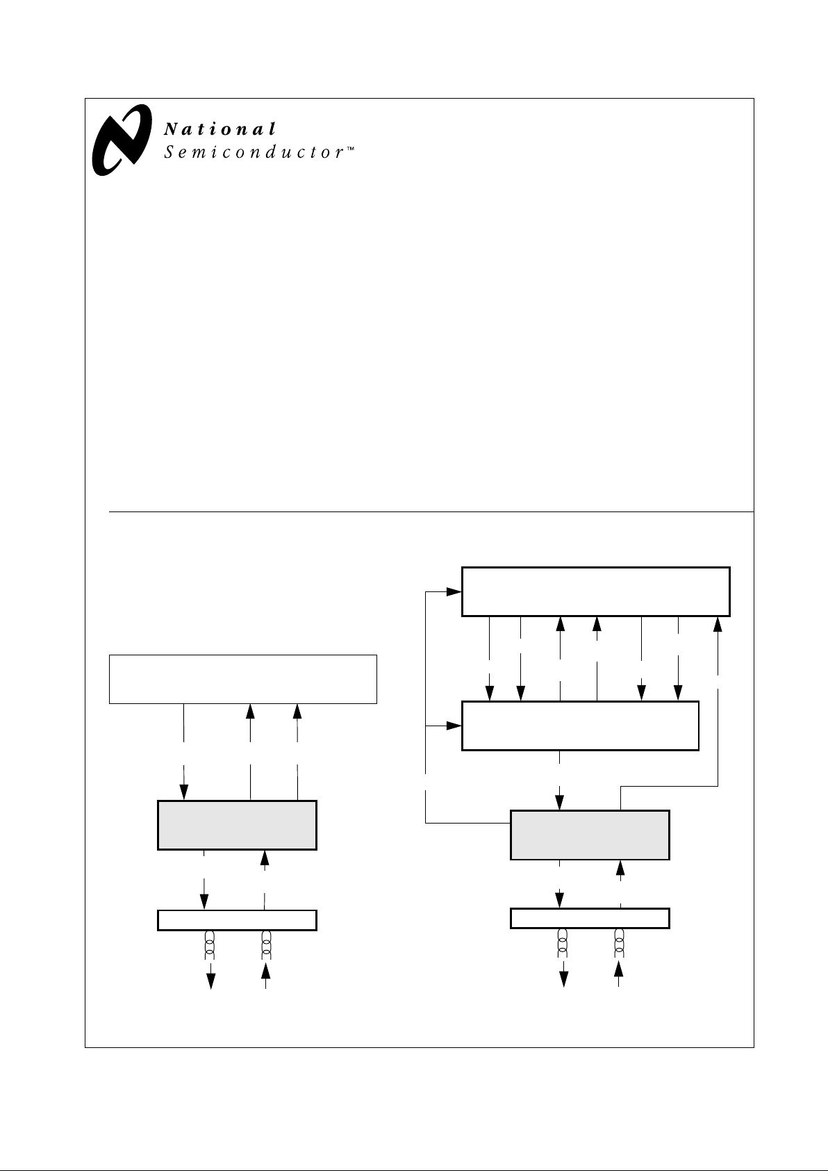
System Connection Diagrams
Features
■ Compatible with ANSI X3.263 TP-PMD draft standard
■ Allows use of Type 1 STP and Category 5 UTP cables
■ Requires a single +5V supply
■ Integrated transmitter and receiver with adaptive equal-
ization circuit
■ Isolated TX and RX power supplies for minimum noise
coupling
■ Loopback feature for board diagnostics
■ Digitally Synthesized transmit signal transition time con-
trol for reduced EMI
■ Programmable transmit voltage amplitude
■ Suitable for 100BASE-TX Fast Ethernet and Twisted
Pair FDDI applications
DP83223 TWISTER High Speed Networking Transceiver Device
April, 1997
DP83223
Transceiver
DP83840A
10/100 Ethernet PHY
Twisted Pair
Magnetics
Media
PMD
Encoded
RXDATA
PMD
Encoded
TXDATA
Scrambled
TX DATA
Signal
Scrambled
RX DATA Detect
100BASE-TX
DP83257VF or DP83256VF-AP
PLAYER+
DP83223
Transceiver
Twisted Pair
Magnetics
DP83222
Stream Cipher
Media
TXC
SIGDET
Phased
RX CLOCK
Recovered
RXCLOCK
TX DATA
Scrambled
TX DATA
PMD
Encoded
RXDATA
PMD
Encoded
TXDATA
Descrambled
RX DATA
Recovered
RX DATA
RXDATA
Twisted Pair FDDI
Page 2
2
Revision A
DP83223
Table of Contents
1.0 Connection Diagram
2.0 Pin Description
3.0 Functional Description
3.1 Overview
3.2 MLT-3 Encoding
3.3 Transition Time Control
3.4 Adaptive Equalization
3.5 Jitter Performance
4.0 DC and AC Specifications
4.1 TRANSMIT TIMING
4.2 RECEIVE PROPAGATION DELAY
4.3 LOOPBACK PROPAGATION DELAY
4.4 SIGNAL DETECT TIMING
4.5 ADAPTIVE EQUALIZER TIMING
General Description (Continued)
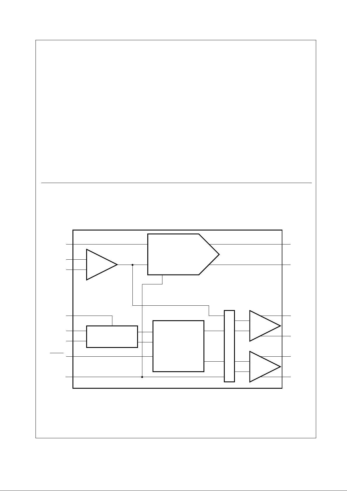
Block Diagram
PMRD+
PMRD-
TXREF
TXO+
TXO-
Comparators/
Control Logic
Equalizer Amp/
Signal Detect
RXI +
RXI -
CDET
EQSEL
MUX LOGIC
LBEN
PMID +
PMID -
SD+
SD-
DATA
SD
Programmable
Current Output
Driver
LB
Page 3
3
DP83223
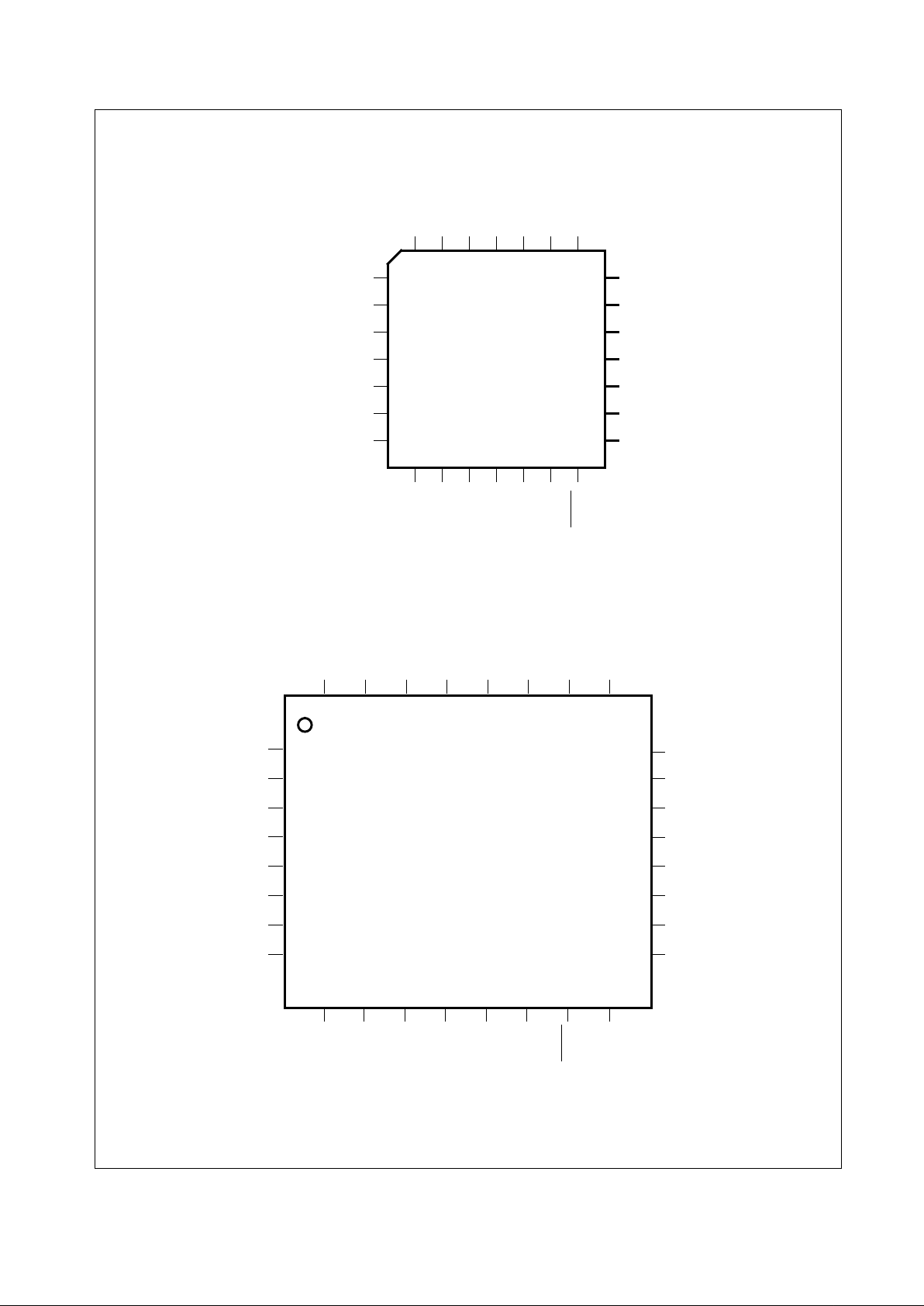
1.0 Connection Diagram
28 Pin PLCC
Order Number DP83223V
See NS Package Number V28A
32 Pin PQFP
Order Number DP83223VBE
See NS Package Number VBE32A
RXI-
RXI+
RXGND
TXREF
TXGND
TXO-
TXO+
TXGND
ENCSEL
GND
PMRD+
PMRD-
EQSEL
CDET
LBEN
SD+
SD-
GND
PMID-
PMID+
RXGND
321282726
4
25
24
23
22
21
20
19
5
6
7
8
9
10
11
12 13 14 15 16 17 18
DP83223V
EXTV
CC
V
CC
TXV
CC
TXV
CC
RXV
CC
RXVCCV
CC
RXI-
RXI+
RXGND
TXREF
TXGND
TXO-
TXO+
TXGND
N/C
ENCSEL
PMRD+
PMRD-
EQSEL
CDET
LBEN
SD+
SD-
GND
PMID-
RXGND
3
2
1
28 27 26425
24
23
22
21
20
19
5
6
7
8
910111213141516
17
18
DP83223VBE
EXTV
CC
V
CC
TXV
CC
TXV
CC
RXV
CC
RXVCCV
CC
GND
N/C
N/C
2932 3031
N/C
PMID+
Page 4

4
DP83223
2.0 Pin Description
DP83223 Pinout Summary
Symbol Pin No
PLCC(PQFP)
Type Description
V
CC
13,26 (10, 25) Supply Vcc: Positive power supply for the ECL compatible circuitry. The
Transceiver operates from a single +5VDC power supply.
GND 14, 22(11 ,20) Supply GND: Return path for the ECL compatible circuitry power supply.
RXVcc 4, 27(26, 31) Supply Receive Vcc: Positive power supply for the small signal receive circuitry.
This power supply is intentionally separated from others to eliminate
receive errors due to coupled supply noise.
RXGND 3, 28(27, 30) Supply Receive GND: Return path for the receive power supply circuitry. This
power supply return is intentionally separated from others to eliminate
receive errors due to coupled supply noise.
TXVcc 5, 11(1, 7) Supply Transmit Vcc: Positive power supply required b y the analog portion of the
transmit circuitry. This power supply is intentionally separated from the
others to prevent supply noise from coupling to the transmit outputs.
TXGND 7, 10(3, 6) Supply Transmit GND: Return path for the analog transmit po wer supply circuitry.
This supply return is intentionally separated from others to prevent supply
noise from being coupled to the transmit outputs.
EXTVcc 23(21) Supply External Vcc: Positive power supply for ECL output circuitry.
RXI+/- 2, 1(29, 28) Differential
Voltage In
Receive Data Inputs: Balanced differential line receiver inputs.
PMID+/- 25, 24(23, 22) ECL Out Physical Media Indicate Data: Differential ECL compatible outputs
source the recovered receive data back to the Physical Layer device or to
a separate clock recovery device.
PMRD+/- 15, 16(12,13) ECL In Physical Media Request Data: Differential ECL compatible inputs which
receive data from Physical Layer Device.
TXO+/- 9, 8(5,4) Differential
Current
Out
Transmit Data Outputs: Differential current driver outputs which drive
MLT-3 encoded data over twisted pair cable. These outputs provide
controlled rise and fall times designed to filter the transmitters output which
helps to reduce associated EMI.
SD+/- 20, 21(18, 19) ECL Out Signal Detect Outputs: Differential ECL compatible Signal Detect outputs
indicating that either a signal with the proper amplitude is present at the
RXI+/- inputs or that Loopback mode has been selected.
TXREF 6(2) Current
Out
Transmit Amplitude Reference: Reference current pin allowing
adjustment of TXO+/- transmit amplitude. By placing a resistor between
this pin and GND, a reference current is setup which results in a given
transmit amplitude for a given application. Refer to Functional Description
in Section 3.1 for reference current equations.
ENCSEL 12(9) CMOS In Encode Select Input: The TTL compatible CMOS Encode Select input
controls the encoded state of the signal at the TXO+/- outputs. A logic low
level at this input causes the TXO outputs to become MLT-3 encoded with
the receiver programmed to accept MLT-3 encoded data. This is the
recommended mode of operation. A logic high level causes the TXO pins
to output standard two-level binary code and the receiver is conditioned to
receive a two-level binary signal. The DP83223V does not guarantee this
mode(binary) of operation.
LBEN 19(17) CMOS In Loopback Enable: TTL compatible CMOS Loopback Enable input pin
selects the internal loopback path which routes the PMRD+/- data to the
PMID+/- differential outputs and forces Signal Detect true. During
loopback, data present at the RXI+/- inputs is ignored. However, binary
data is still transmitted by the TXO+/- outputs (regardless of the state of the
ENCSEL input). Loopback mode is selected when LBEN is forced high.
Normal operation occurs when LBEN is forced low.
Page 5

2.0 Pin Description (Continued)
5Revision A
DP83223
EQSEL 17(14) 3-Level Se-
lect
Equalization Select: This three level Equalization Select input controls the
mode of receiver equalization. Forcing a median voltage level,
accomplished by allowing EQSEL to float, selects the adaptive
equalization mode which automatically regulates the equalization effects
based on signal degradation caused by the media. The other two le vels are
intended as test modes and are not a guaranteed mode of operation.
Forcing a voltage less than 1.5V, selects full equalization which provides
fixed equalization for a maximum length of cab le. F orcing a v oltage greater
than 3.0V turns the receive equalizer off.
CDET 18(15) CMOS In Cable Detect Bar: The active low Cable Detect CMOS input is provided to
support the option of external Cable Detection circuitry (wire fault). With
CDET low, the tr ansceiver functions normally. With CDET high, the signal
detect output is forced low which inhibits data reception by the PHY and
the PMID outputs are forced to ECL static levels. The exception is in the
case of Loopback when the Signal Detect output is forced high regardless
of all other conditions. Please refer to the National Semiconductor Com-
mon Magnetics application note for further detail regarding the proper use
of the DP83223 in a 10/100 Ethernet application.
Symbol Pin No
PLCC(PQFP)
Type Description
Page 6

6
Revision A
DP83223
3.0 Functional Description
3.1 Overview
The DP83223 transceiver consists of the major functional
blocks shown in the “Block Diagram”. The Transmit section consists of an ECL input buffer for PMRD+/- and the
Programmable Current Output Driver. The Programmable
Current Output Driver can be configured to convert the
incoming binary datastream to a current sourced MLT-3
encoded datastream.
The transmit amplitude of the signal presented at the TXO
output pins can be controlled by varying the value of resistance between TXREF and GND. This TXREF resister,
R
REF
, sets up a reference current which determines the
final output current at TXO+/- as described by:
The following equation yields the differential peak-peak
transmit voltage for a given characteristic cable impedance:
The transition times at the TXO+/- outputs are of special
interest. These matched rise and fall times are digitally
synthesized to reduce EMI emissions at the media interface and on the media. The controlled transition times
also significantly reduce the design complexity and cost
by minimizing external filtering.
The Receive section consists of the following functional
blocks: a differential input Equalization Amplifier with Signal Detect circuitry, signal Comparators with Control
Logic, Loopback Multiplexer Logic, and differential ECL
output drivers for PMID and Signal Detect.
In adaptive or full equalization mode, as selected by the
EQSEL input pin, the receive data is first equalized and
then amplified for signal detection. If the receive equalizer
is turned off, the data is then only amplified for signal
detection.
The Comparator and Control Logic Block performs several functions. Primarily, the comparators quantize and
convert incoming MLT-3 into binary. The control logic
receives input from
CDET and ENCSEL enabling final signal detect indication and control of data conversion/regeneration.
The Loopback Mux logic performs the function of routing
the transmit data at the PMRD+/- inputs to either the
PMID+/- pins (loopback enabled) or directly to the TXO+/current outputs (normal operation).
Finally, ECL output drivers are used to drive both PMID+/receive data and SD+/- Signal Detect data to the appropriate Physical Layer device.
3.2 MLT-3 Encoding
The decision to incorporate MLT-3 (Multi-Level-Transmit /
3 levels) signal encoding into the ANSI X3.263 Twisted
Pair Standard is based solely on the issue of Electro-Magnetic Compatibility (EMC). Scrambling the datastream, via
the Stream Cipher function, reduces EMI emissions at key
frequencies by approximately 20dB. Although 20dB is significant, it may be insufficient to pass the FCC Class B
radiation limit (with margin) for NRZI signalling at the standard transmit amplitude of 2.0V. The inclusion of MLT-3
encoding theoretically provides an additional 3dB reduction in EMI emissions depending on the measurement
technique and system design/layout.
The effect of MLT-3 encoding is the reduction of energy on
the media in the critical frequency range of 20MHz to
100MHz. This is achieved by trading line frequency for
line voltage complexity. When a binary data stream is
MLT-3 encoded, the result is a shift, in part, of some frequency components of the signal.
See Figure 3-1, the second ‘high’ pulse in the binary
waveform is transformed by an inversion to the ‘-1’ lev el in
the MLT-3 waveform. This inversion corresponds to a certain decrease in energy from the original binary frequency
component. The decrease in energy at the critical frequency of 62.5MHz is appreciable (3dB to 6dB).
Figure 3-1. Example of Binary vs. MLT-3
The power spectrum plots in Figure 3-2 and Figure 3-3
provide a clear comparison between scrambled binary
and scrambled MLT-3 respectively. It should be noted that
FCC Class B limits relate to radiated emissions and not
the direct power spectrum. The plots in Figure 3-2 and
Figure 3-3 are intended strictly for use as a general comparison between Binary and MLT-3 and should not be
interpreted as absolute EMI performance indicators.
Figure 3-2. 1V Binary Power Spectrum
I
TXO
= 20.48
R
REF
V
OUTpk-pkdiff
= I
TXO * Zcable
2
01010 1 01
Binary
MLT-3
11
010-10 1 01-1-1
10 dB / div
0 MHz 125MHz 250MHz
Page 7

3.0 Functional Description (Continued)
7
Revision A
DP83223
Figure 3-3. 2V MLT-3 Power Spectrum
3.3 Transition Time Control
The DP83223 TWISTER incorporates a unique feature
which virtually eliminates the need for external filtering of
the transmitted signal. The transition times of the TXO
output signals are digitally synthesized resulting in closely
matched and controlled rise and fall times (Refer to Figure 3-4). These controlled transition times, in conjunction
with the associated magnetics, result in typical rise and
fall times of greater than 3ns. These transition times lie
within the range specified in the X3.263 Twisted Pair PMD
standard.
Figure 3-4. Controlled TXO Transitions
3.4 Adaptive Equalization
When transmitting data at high speeds over copper
twisted pair cable, frequency dependent attenuation
becomes a concern. In Twisted Pair Fast Ethernet or
FDDI signalling the frequency content of the transmitted
signal can vary greatly during normal operation based primarily on the randomness of the scrambled data stream.
This variation in signal attenuation caused by frequency
variations must be compensated for to ensure the integrity
of the transmission.
In order to ensure quality transmission when employing
MLT-3 encoding, the compensation must be able to adapt
to various cable lengths and cable types depending on the
installed environment. In a fixed equalization system, the
selection of long cable lengths for a given implementation,
requires significant compensation which will over-compensate for shorter, lower attenuation lengths . Con v ersely,
the selection of short or intermediate cable lengths requiring less compensation will cause serious under-compensation for longer length cables. Therefore, the
compensation (equalization) must be adaptive to ensure
proper conditioning of the received signal independent of
cable length.
The combination of choosing MLT-3 as the signal encoding scheme, in conjunction with a requirement for adaptive
equalization, demands that compensation occur at the
receive end of the transmission network. In order to implement receiver adaptive equalization, a known relationship
between transmit output amplitude and a receive input
reference must be specified and controlled. Nominal
transmit output amplitude, as specified by the ANSI
X3.263 TP-PMD document, is 2.0V peak to peak differential. The DP83223 TWISTER incorporates a fixed nominal
receive input reference. Given these two parameters, the
adaptive equalization can determine the approximate
cable length via signal attenuation at certain frequencies
and actively compensate for cable length variations.
Since the DP83223 TWISTER transceiver’s receive input
reference is fixed at approximately 1.45V and the transmit
amplitude is fixed at 2.0V, an attenuation factor is
required. This attenuation is accomplished by a simple
resistive voltage divider placed at the RXI+/- inputs, which
also serves as the forward termination for the transmission line (Refer to Figure 4-3). Because the voltage
divider attenuates any noise along with the received signal, the Signal-to-Noise ratio is not decreased. An additional benefit is gained by including the voltage divider,
where any insertion loss caused by the media coupling
magnetics can be compensated for by adjusting the voltage divider ratio. This will ensure appropriate signal transfer and optimal adaptive equalization.
For additional information regarding the interdependencies between the adaptive equalizer and the receive
attenuation/termination circuit, refer to the NSC application note entitled “DP83223 Adaptive Equalizer Considerations”.
3.5 Jitter Performance
This section briefly presents the typical jitter performance
exhibited by the DP83223 TWISTER transceiver. The
DP83223 TWISTER was subjected to the near worstcase condition of 110 Meters of Category 5 cable connected to two lengths of 10Meter cable via two 110
punchdown blocks (totalling 130 Meters). The DP83223
10 dB / div
0 MHz 125MHz 250MHz
Page 8

3.0 Functional Description (Continued)
8
Revision A
DP83223
TWISTER was loaded with pseudo random data (PRBS-
23) approximating actual packet data encrypted via the
stream cipher algorithm. The typical peak-peak total jitter
resulting from the combination of the transmitter, cable
plant, and receiver is only 1.9ns Pk-Pk (MLT-3, room
temp., nominal Vcc) as illustrated in Figure 3-5. Because
the maximum eye opening is 8ns, The DP83223 has little
impact on the total jitter budget.
Figure 3-5. MLT-3 Total Jitter=1.9ns Pk-Pk
2ns / div
Page 9

9
DP83223
4.0 DC and AC Specifications
Absolute Maximum Ratings
Supply Voltage (VCC) -0.5 V to 7.0 V
Recieved Power (RXV
CC
V) -0.5 V to 7.0 V
Transmitted Power (RXV
CC
V) -0.5 V to 7.0V
Storage Temperature Range (T
STG
)
-65
o
C to 150oC
Power Dissipation (P
D
) 1.575 W
I
ECl
-50 mA
Lead Temp. (T
L
) (Soldering, 10 sec)
260
o
C
Recommended Operating Conditions
Note:
Absolute maximum ratings are those values beyond
which the safety of the device cannot be guaranteed. They
are not meant to imply that the device should be operated
at these limits.
ESD Rating
(R
ZAP
= 1.5k, C
ZAP
= 120 pF)
2.0 KV
Supply voltage (VDD) 5 Volts + 5%
Ambient Temperature (T
A
)
0 to 70
o
C
DC Specifications TA = 0
o
C to 70oC, VCC = 5 V 5%, unless otherwise specified
Symbol Parameter Conditions Min Max Units
I
IHt
TTL High Level Input VIN= Vcc 10 uA
I
ILt
TTL Low Level Input VIN= GND -10 uA
I
IHcdet
CDET High Level Input VIN= Vcc 10 uA
I
ILcdet
CDET Low Level Input VIN= GND -10 uA
I
IHeqsel
EQSEL High Level Input VIN= Vcc 800 uA
I
ILeqsel
EQSEL Low Level Input VIN= GND -800 uA
I
IHe
ECL High Level Input VIN= Vcc - 830 mV 50 uA
I
ILe
ECL Low Level Input VIN= Vcc - 1570mV 1 uA
V
IHt
TTL High Level Input 2 V
V
ILt
TTL Low Level Input 0.8 V
V
IHcdet
CDET High Level Input note 2 Vcc-1 V
V
ILcdet
CDET Low Level Input note 2 1 V
V
IMeqsel
EQSEL Mid Level Input note 3 Vcc / 2 V
V
IHe
ECL High Level Input Vcc-
1165
Vcc-880 mV
V
ILe
ECL Low Level Input Vcc-
1810
Vcc-
1475
mV
V
OHe
ECL High Level Output Vcc-
1075
Vcc-830 mV
V
OLe
ECL Low Level Output Vcc-
1860
Vcc-
1570
mV
I
CC
Dynamic Supply Current notes 4 & 5, Figure 4-1 135 mA
I
TXO
Transmit Current note 6, Figure 4-1 38.2 40 41.8 mA
I
TX-
Omatch
Transmit Current Matching note 7, Figure 4-1 -2 2 %
SD
THon
Sig Det Assert Threshold note 8, Figure 4-2 700 mV
SD
THoff
Sig Det De-assert Threshold notes 1 & 9, Figure 4-2 200 mV
R
INdiff
RXI differential input resistance 7 9 KΩ
Page 10

4.0 DC and AC Specifications (Continued)
10
DP83223
Note 1:Guaranteed by characterization over process, temperature, and Vcc.
Note 2:It is recommended that the
CDET control input be tied directly to Vcc or GND to ensure proper operation. IfCDET is to be driven from a gate, it is
recommended that the gate be capable of true CMOS logic levels.
Note 3:The median voltage level for EQSEL is normally accomplished by floating that pin.
Note 4:ICC is a measure of total device current in normal MLT-3 mode with a 125Mb/s random data pattern applied to the PMRD+/- inputs to allow the
TXO+/- outputs to switch at a nominal 2V pk-pk differential amplitude into a standard 50Ω differential load. ICC is minus the current through the PECL inputs.
Device configuration: LBEN=0,
CDET=0, ENCSEL=0, EQSEL=float, PMRD+/-=125Mb/s data, RXI+/-=125Mb/s data.
Note 5:ICC does not include the current through the PECL outputs. Standard 50Ω Thevenin equivalent PECL terminations (figure 10) require approximately
14 mA per pin, or a total of 56 mA. 100Ω PECL terminations require approximately 7 mA per pin, or a total of 28 mA. These external PECL termination current
requirements should be considered when analyzing system power requirements.
Note 6:TXO output current is a measure of the total differential current present at the TXO+/- outputs into a standard 50Ω differential load. Device configu-
ration: R
REF
=510Ω, LBEN=0, CDET=0, ENCSEL=0, EQSEL=float, RXI+/-=static.
Note 7:I
TXOmatch
refers to the percentage of mismatch in current between TXO+ and TXO- referenced to the total output current as defined by:
Device configuration: R
REF
=510Ω, ENCSEL=0, PMRD+=0, PMRD-=1.
Note 8:Signal Detect Assert Threshold is a measure of the pk-pk differential signal amplitude at the RXI+/- inputs of the RJ45 required to cause the Signal
Detect differential output to assert. Device configuration: LBEN=0,
CDET=0, ENCSEL=0, EQSEL=float, PMRD+/-=static, RXI+/-=125Mb/s data with swept
amplitude.
Note 9:Signal Detect De-assert Threshold is a measure of the pk-pk differential signal amplitude at the RXI+/- inputs of the RJ45 required to cause the Signal
Detect differential output to de-assert. Device configuration: LBEN=0, CDET=0, ENCSEL=0, EQSEL=float, PMRD+/-=static, RXI+/-=125Mb/s data with
swept amplitude
Figure 4-1. ICC / Load Diagram
I
TXO+
- I
TXO-
I
TXO++ITXO-
x 100
I
TXOmatch
=
TXVCC
RXVCC
VCC
EXTVCC
SD+
SD-
PMID+
PMID-
TXO+ TXO-TXGND RXGND GND
VCC
+
-
DP83223
25Ω
25Ω
VCC - 2V
+
-
50Ω
TXREF
510Ω
50Ω 50Ω 50Ω
ICC
ICC
external
Page 11

4.0 DC and AC Specifications (Continued)
11
DP83223
Figure 4-2. Post Equalized Signal Detect Voltage
Figure 4-3.
Typical Schematic for 100BASE-TX signalling over Cat-5 UTP 100Ω cable
Active PMID
Inactive PMID
SD
THoff
SD
THon
Post Equalized Signal Detect Voltage
DP83223
TXO+
TXGND
TXO-
GND
TXREF
RXI-
RXI+
SD+
SD-
ENCSEL
PMRD+
PMRD-
RXGND
EQSEL
LBEN
PMID+
PMID-
R
REF
RJ-45
CDET
EXTVCC
VCC
TXVCC
RXVCC
V
CC
Contact National Semiconductor
for further information relating to
available magnetics modules
VCC
FB
GND
Data from
PHY
Device
SD To PHY
Device
Data to PHY or
Clock Recovery
The PMRD, SD and PMID 100K ECL differential signal must be
terminated into a standard ECL load of 50Ω to VCC-2.0V or equivalent:
i.e. Thevenin of 130Ω to GND accompanied by 82Ω to VCC
= Murata # BLM31A02PT (1206 package)
FB
*510Ω
1
2
3
4
5
6
7
8
Transmit
Magnetics
Receive
Magnetics
float
37.9Ω
All resistors are 1/10th Wt, 1% tolerance
Device
37.9Ω
12.1Ω 12.1Ω
0.01uF
0.01uF
50Ω
50Ω
0.01uF
The Receive Attenuation / Termination network
must be optimized to compensate for the insertion
loss of the receive magnetics.
Please refer to the National Semiconductor Application Note
entitled “DP83223 Adaptive Equalization Considerations”
for further detail. The values provided in this example
are targeted to match an insertion loss of approximately
0.4dB (approximately 90mV pk-pk differential of loss for
a typical scrambled IDLE line state) which will result in
All capacitors are 16V ceramic
Common Mode Noise Filter
*The Rref resistor value may need to be adjusted
to compensate for transmit magnetics insertion
loss in order to achieve the standard specific
2.0V pk-pk differential TXO+/- output amplitude
as measured across the RJ45 transmit pins.
a final amplitude of approximately 1.45V pk-pk differential
as seen across the RXI+/- inputs for zero Meters of cable.
Page 12

4.0 DC and AC Specifications (Continued)
12
DP83223
4.1 TRANSMIT TIMING
Note: TXO Output Rise and Fall time is a measure of the transition time for all MLT-3 transitions from 10% to 90%. This measurement is conducted directly
at the TXO+/- outputs and does not include the additional bandwidth limiting effects of an isolation transformer. Each of the four possible MLT-3 transitions
is measured (see figure 2 for MLT-3 waveform example). The TXO+/- outputs are configured to switch at a nominal 2V pk-pk differential amplitude into a
standard 50Ω differential load. Device configuration: LBEN=0,
CDET=0, ENCSEL=0, EQSEL=float, PMRD+/-=125Mb/s data, RXI+/-=static.
Note: : t
TXr/fsym
TXO Rise and Fall Symmetry is the difference between the maximum and minimum of all rise and fall times. Device configuration: LBEN=0,
CDET=0, ENCSEL=0, EQSEL=float, PMRD+/-=125Mb/s data, RXI+/-=static.
Note: : The Transmit channel propagation delay is a measure of the time delay imposed on the transmit data as it passes from the PMRD+/- inputs to the
TXO+/- outputs. Device configuration: LBEN=0,
CDET=0, ENCSEL=0, EQSEL=float, PMRD+/-=125Mb/s data, RXI+/-=static.
Note: Transmit Jitter is a measure of the total jitter as measured differentially across the TXO+/- outputs of the device. This includes the cumulative effect
of Duty Cycle Distortion (DCD), Data Dependent Jitter (DDJ), and Random Jitter (RJ). Device configuration: LBEN=0,
CDET=0, ENCSEL=0, EQSEL=float,
PMRD+/-=125Mb/s data (pseudo random ^15), RXI+/-=125Mb/s data in order to induce a worst case system level noise environment.
Note: T1.1, T1.2 and T1.4 are guaranteed by characterization over process, temperature, and Vcc.
4.2 RECEIVE PROPAGATION DELAY
Note: The Receive channel propagation delay is a measure of the time delay imposed on the receive data as it passes from the RXI+/- inputs to the PMID+/-
outputs. This measurement is taken after the device has had sufficient time for the receive adaptive equalizer to converge. Device configuration: LBEN=0,
CDET=0, ENCSEL=0, EQSEL=float, PMRD+/-=static, RXI+/-=125Mb/s data.
Number Parameter Min Typ Max Units
T1.1
TXO Output Rise and Fall 2.25 2.75 3.25 ns
T1.2
TXO Rise / Fall Symmetry 500 ps
T1.3
TX prop delay 7 ns
T1.4
Transmit Jitter 1.4 ns
Number Parameter Min Typ Max Units
T2.1 Receive Propagation Delay 7 ns
T2.1
RXI+
RXI-
PMID+
PMID-
PMRD+
PMRD-
TXO+
TXO-
T1.3
T1.1
10% - 90%
T1.1
1
0
-1
TXO-
TXO+
Page 13

Do Not Use
4.3 LOOPBACK PROPAGATION DELAY
4.4 SIGNAL DETECT TIMING
Note: The Signal Detect Assert Time is a measure of the time required for Signal Detect to assert after the RXI+/- inputs are provided with a receive signal
with sufficient amplitude to meet the Signal Detect Assert Threshold parameter. Device configuration: LBEN=0,
CDET=0, ENCSEL=0, EQSEL=float, PM-
RD+/-=static, RXI+/-=125Mb/s data with amplitude greater than 700mV pk-pk differential.
Note: The Signal Detect De-assert Time is a measure of the time required for Signal Detect to deassert after the RXI+/- inputs are provided with a receive
signal with sufficient amplitude to meet the Signal Detect Deassert Threshold parameter. Device configuration: LBEN=0, CDET=0, ENCSEL=0,
EQSEL=float, PMRD+/-=static, RXI+/-=125Mb/s data with amplitude less than 200mV pk-pk differential.
4.5 ADAPTIVE EQUALIZER TIMING
Note: Total Receive Jitter is a measure of the total accumulated jitter as measured differentially across the PMID+/- receive outputs of the device. This pa-
rameter is guaranteed by an ATE adaptive equalizer jitter measurement (done at worst case conditions) and a system level characterization over temperature
and Vcc. The ATE measurement has been empirically correlated with the system level jitter measurement, which includes all transmit jitter (as described in
T1.3) as well as all jitter induced by a worst case Cat-5 cable plant and the additional Jitter induced by the receive operation of the device. Device configuration: LBEN=0,
CDET=0, ENCSEL=0, EQSEL=float, PMRD+/-=125Mb/s data, RXI+/-=125Mb/s data.
Number Parameter Min Typ Max Units
T3.1 Loopback Propagation Delay 7 ns
Number Parameter Min Typ Max Units
T4.1 Signal Detect Turn-On Time
40 100 us
T4.2 Signal Detect Turn-Off Time
12 50 us
Number Parameter Min Typ Max Units
T5.1
Total Jitter (TX+RX) 2 3.5 ns
PMRD+
PMRD-
PMID+
PMID-
T3.1
SD+
RXI +/-
signal
static
static
T4.1
T4.2
Page 14

Do Not Use
LIFE SUPPORT POLICY
NATIONAL'S PRODUCTS ARE NOT AUTHORIZED FOR USE AS CRITICAL COMPONENTS IN LIFE SUPPOR
T
DEVICES OR SYSTEMS WITHOUT THE EXPRESS WRITTEN APPROVAL OF THE PRESIDENT OF NATIONA
L
SEMICONDUCTOR CORPORATION. As used herein:
2. A critical component is any component of a life support
device or system whose failure to perform can be
reasonably expected to cause the failure of the life support
device or system, or to affect its safety or effectiveness.
.Life support devices or systems we do or systems
which, (a) are intended for surgical implant into the
body , or (b) support or sustain life , and whose f ailure to
perform, when properly used in accordance with
instructions for use provided in the labeling, can be
reasonably expected to result in a significant injury to
the user.
National Semiconductor
Corporation
1111 West Bardin Road
Arlington, TX 76017
Tel: 1(800) 272-9959
Fax: 1(800) 737-7018
National Semiconductor
Corporation
Europe
Fax:(+49) 0-180-530 85 86
Email:cnjwge@tevm2.nsc.com
Duetsch Tel: (+49) 0-180-530 85 86
English Tel: (+49) 0-180-532 78 32
Francais Tel: (+49) 0-180-532 93 58
Italiano Tel: (+49) 0-180-534 16 80
National Semiconductor
Corporation
Japan Ltd.
Tel: 81-043-299-2308
Fax: 81-043-299-2408
National Semiconductor
Corporation
Hong Kong Ltd.
13th Floor, Straight Block,
Ocean Centre, 5 Canton Rd.
Tsimshatsui, Kowloon
Hong Kong
Tel: (852) 2737-1600
Fax: (852) 2736-9960
 Loading...