

Page 1
DP8310/DP8311
Octal Latched Peripheral Drivers
General Description
The DP8310 and DP8311 Octal Latched Peripheral Drivers
provide the function of latching eight bits of data with open
collector outputs, each driving up to 100 mA DC with an operating voltage range of 30V. Both devices are designed for
low input currents, high input/output voltages, and feature a
power up clear (outputs off) function.
The DP8310 is positive edge latching. Two active low write/
enable inputs are available forconvenientdatabussingwithout external gating.
The DP8311 is positive edge latching. The active low strobe
input latches data or allows fall through operation when held
at logic “0”. The latches are cleared (outputs off) with a logic
“0” on the clear pin.
Features
n High current, high voltage open collector outputs
n Low current, high voltage inputs
n All outputs simultaneously sink rated current “DC” with
no thermal derating at maximum rated temperature
n Parallel latching or buffering
n Separate active low enables for easy data bussing
n Internal “glitch free” power up clear
n 10%V
CC
tolerance
Applications
n High current high voltage drivers
n Relay drivers
n Lamp drivers
n LED drivers
n TRIAC drivers
n Solenoid drivers
n Stepper motor drivers
n Level translators
n Fiber-optic LED drivers
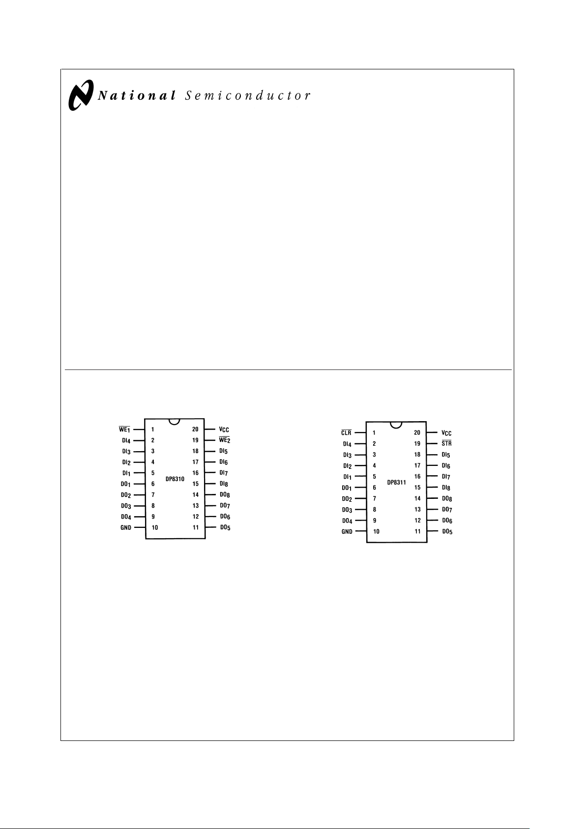
Connection Diagrams
Dual-In-Line Package
DS005246-1
Top View
Dual-In-Line Package
DS005246-2
Top View
Order Number DP8310N or DP8311N
See NS Package Number N20A
February 2000
DP8310/DP8311 Octal Latched Peripheral Drivers
© 2000 National Semiconductor Corporation DS005246 www.national.com
Page 2
Absolute Maximum Ratings (Note 1)
If Military/Aerospace specified devices are required,
please contact the National Semiconductor Sales Office/
Distributors for availability and specifications.
Supply Voltage 7.0V
Input Voltage 35V
Output Voltage 35V
Maximum Power Dissipation
*
at T
A
=
25˚C
DP8310/DP8311 2005 mW
Storage Temperature Range −65˚C to +150˚C
Lead Temperature (Soldering, 4 sec.) 260˚C
Note:*Derate N20A package 15.4 mW/˚C above T
A
=
25˚C, θJ
A
=
65˚C/W.
Operating Conditions
Min Max Units
Supply Voltage (V
CC
) 4.5 5.5 V
Temperature
DP8310/DP8311 0 +70 ˚C
Input Voltage 30 V
Output Voltage 30 V
DC Electrical Characteristics
DP8310 and DP8311 (Notes 2, 3)
Symbol Parameter Conditions Min Typ Max Units
V
IH
Logical “1” Input Voltage 2.0 V
V
IL
Logical “0” Input Voltage 0.8 V
V
OL
Logical “0” Output Voltage Data outputs latched to
logical “0”, V
CC
=
Min.
DP8310/DP8311 I
OL
=
100 mA 0.35 0.5 V
I
OH
Logical “1” Output Current Data outputs latched to
logical “1”, V
CC
=
Min.
DP8310/DP8311 V
OH
=
30V 2.5 250 µA
I
IH
Logical “1” Input Current V
IH
=
2.7V, V
CC
=
Max 0.1 25 µA
I
I
Input Current at Maximum Input
Voltage
V
IN
=
30V, V
CC
=
Max
1 250 µA
I
IL
Logical “0” Input Current V
IN
=
0.4V, V
CC
=
Max −215 −300 µA
V
clamp
Input Clamp Voltage I
IN
=
12 mA −0.8 −1.5 V
I
CC0
Supply Current, Outputs On Data outputs latched to a
logical “0”. All Inputs are
at logical “1”, V
CC
=
Max.
DP8310 100 152 mA
DP8311 88 125 mA
I
CC1
Supply Current, Outputs Off Data outputs latched to a
logic “1”. Other
conditions same as I
CC0
.
DP8310 40 57 mA
DP8311 25 36 mA
AC Electrical Characteristics
DP8310 only: V
CC
=
4.5V, T
A
=
25˚C
Symbol Parameter Conditions Min Typ Max Units
t
pd0
High to Low Propagation Delay
Write Enable Input to Output
(Figure 1 )
40 120 ns
t
pd1
Low to High Propagation Delay
Write Enable Input to Output
(Figure 1 )
70 150 ns
t
SETUP
Minimum Set-Up Time
Data in to Write Enable Input
t
HOLD
=
0ns
(Figure 1)
45 20 ns
t
pWH,tpWL
Minimum Write Enable Pulse Width
(Figure 1 )
60 25 ns
t
THL
High to Low Output Transition Time
(Figure 1 )
16 35 ns
t
TLH
Low to High Output Transition Time
(Figure 1 )
38 70 ns
C
IN
“N” Package (Note 4) 5 15 pF
DP8310/DP8311
www.national.com 2
Page 3
AC Electrical Characteristics
DP8311 only: V
CC
=
5V, T
A
=
25˚C
Symbol Parameter Conditions Min Typ Max Units
t
pd0
High to Low Propagation Delay
Data In to Output
(Figure 2 )
30 60 ns
t
pd1
Low to High Propagation Delay
Data to Output
(Figure 2)
70 100 ns
t
SETUP
Minimum Set-Up Time
Data in to Strobe Input
t
HOLD
=
0ns
(Figure 2 )
0 −25 ns
t
pWL
Minimum Strobe Enable Pulse Width
(Figure 2 )
60 35 ns
t
pdC
Propagation Delay Clear to Data Output
(Figure 2 )
70 135 ns
t
pWC
Minimum Clear Input Pulse Width
(Figure 2 )
60 25 ns
t
THL
High to Low Output Transition Time
(Figure 2 )
20 35 ns
t
TLH
Low to High Output Transition Time
(Figure 2 )
38 60 ns
C
IN
Input Capacitance — Any Input (Note 4) 5 15 pF
Note 1: “AbsoluteMaximum Ratings” are those values beyond which the safety of the device cannot be guaranteed. Except for “Operating TemperatureRange” they
are not meant to imply that the devices should be operated at these limits. The table of “Electrical Characteristics” provides conditions for actual device operation.
Note 2: Unless otherwise specified min/max limits apply across the 0˚C to +70˚C for the DP8310/DP8311. All typical values are for T
A
=
25˚C, V
CC
=
5V.
Note 3: All currents into device pins shown as positive, out of device pins as negative, all voltages referenced to ground unless otherwise noted.
Note 4: Input capacitance is guaranteed by periodic testing. f
TEST
=
10 kHz at 300 mV, T
A
=
25˚C.
DP8310/DP8311
www.national.com3
Page 4

Logic Table
DP8310
Write
Enable 1
WE
1
Write
Enable 2
WE
2
Data
Input
DI
1–8
Data
Output
DO
1–8
00XQ
0
O
01
0
O
10
O
001
O
010
01XQ
10XQ
11XQ
DP8311
Clear
CLR
Strobe
STR
Data
Input
DI
1–8
Data
Output
DO
1–8
11XQ
1001
1010
0XX1
X
=
Don’t Care
1=Outputs Off
0=Outputs On
Q=Pre-existing Output
O
=
Positive Edge Transition
Block Diagrams
DP8310
DS005246-3
DP8311
DS005246-4
DP8310/DP8311
www.national.com 4
Page 5

Switching Time Waveforms
Switching Time Test Circuits
DP8310
DS005246-5
DP8311
DS005246-6
DS005246-7
*
WE
1
=
0V When the Input=WE
2
FIGURE 1. DP8310
DS005246-8
Pulse Generator Characteristics:
Z
O
=
50Ω,t
r
=
t
f
=
5ns
FIGURE 2. DP8311
DP8310/DP8311
www.national.com5
Page 6

Typical Applications DP8310/11 Buffering High Current Device (Notes 5, 6)
PNP High Current Driver
DS005246-9
NPN High Current Driver
DS005246-10
VMOS High Current Driver
DS005246-11
Circuit Used to Reduce Peak
Transient Lamp Current
DS005246-12
DP8310/DP8311
www.national.com 6
Page 7

Typical Applications DP8310/11 Buffering High Current Device (Notes 5, 6) (Continued)
Eight Output/Four Output Fiber Optic LED Driver
DP8311 100 mA Drivers
DS005246-13
DP8311 Parallel Outputs (200 mA) Drivers
*
DS005246-14
*
Parallel only adjacent outputs
8-Bit Level Translator Driver
DS005246-15
Digital Controlled 256 Level
Power Supply from 1.2V to 30V
DS005246-16
DP8310/DP8311
www.national.com7
Page 8

Typical Applications DP8310/11 Buffering High Current Device (Notes 5, 6) (Continued)
200 mA Drive for a 4 Phase Bifilar Stepper Motor
DS005246-17
*
Parallel only adjacent outputs
Reading the State of the Latched Peripherals
DS005246-18
*
High Level Input
Voltage must not
Exceed V
CC
of the
DM81LS96
Note 5: Always use good V
CC
bypass and ground techniques to suppress transients caused by peripheral loads.
Note 6: Printed circuit board mounting is required if these devices are operated at maximum rated temperature and current (all outputs on DC).
DP8310/DP8311
www.national.com 8
Page 9

Physical Dimensions inches (millimeters) unless otherwise noted
LIFE SUPPORT POLICY
NATIONAL’S PRODUCTS ARE NOT AUTHORIZED FOR USE AS CRITICAL COMPONENTS IN LIFE SUPPORT
DEVICES OR SYSTEMS WITHOUT THE EXPRESS WRITTEN APPROVAL OF THE PRESIDENT AND GENERAL
COUNSEL OF NATIONAL SEMICONDUCTOR CORPORATION. As used herein:
1. Life support devices or systems are devices or
systems which, (a) are intended for surgical implant
into the body, or (b) support or sustain life, and
whose failure to perform when properly used in
accordance with instructions for use provided in the
labeling, can be reasonably expected to result in a
significant injury to the user.
2. A critical component is any component of a life
support device or system whose failure to perform
can be reasonably expected to cause the failure of
the life support device or system, or to affect its
safety or effectiveness.
National Semiconductor
Corporation
Americas
Tel: 1-800-272-9959
Fax: 1-800-737-7018
Email: support@nsc.com
National Semiconductor
Europe
Fax: +49 (0) 180-530 85 86
Email: europe.support@nsc.com
Deutsch Tel: +49 (0) 69 9508 6208
English Tel: +44 (0) 870 24 0 2171
Français Tel: +33 (0) 1 41 91 8790
National Semiconductor
Asia Pacific Customer
Response Group
Tel: 65-2544466
Fax: 65-2504466
Email: ap.support@nsc.com
National Semiconductor
Japan Ltd.
Tel: 81-3-5639-7560
Fax: 81-3-5639-7507
www.national.com
Molded Dual-In-Line Package (N)
Order Number DP8310N or DP8311N
NS Package Number N20A
DP8310/DP8311 Octal Latched Peripheral Drivers
National does not assume any responsibility for use of any circuitry described, no circuit patent licenses are implied and National reserves the right at any time without notice to change said circuitry and specifications.
 Loading...