

Page 1

February 1996
DP7304B/DP8304B 8-Bit TRI-STATE Bidirectional Transceiver (Non-Inverting)
DP7304B/DP8304B 8-Bit TRI-STATE
É
Bidirectional Transceiver (Non-Inverting)
General Description
The DP73048B/DP8304B are high speed Schottky 8-bit
TRI-STATE bidirectional transceivers designed to provide
bidirectional drive for bus oriented microprocessor and digital communications systems. They are all capable of sinking
16 mA on the A ports and 48 mA on the B ports (bus ports).
PNP inputs for low input current and an increased output
high (V
other technologies that have a higher threshold and less
drive capabilities. In addition, they all feature glitch-free
power up/down on the B port preventing erroneous glitches
on the system bus in power up or down.
DP7304B/DP8304B are featured with Transmit/Receive
(T/R) and Chip Disable (CD) inputs to simplify control logic.
) level allow compatibility with MOS, CMOS, and
OH
Logic and Connection Diagrams
Features
Y
8-bit bidirectional data flow reduces system package
count
Y
Bidirectional TRI-STATE inputs/outputs interface with
bus oriented systems
Y
PNP inputs reduce input loading
Y
Output high voltage interfaces with TTL, MOS, and
CMOS
Y
48 mA/300 pF bus drive capability
Y
Pinouts simplify system interconnections
Y
Transmit/Receive and chip disable simplify control logic
Y
Compact 20-pin dual-in-line package
Y
Bus port glitch free power up/down
Dual-In-Line Package
TL/F/8793– 1
Order Number DP7304BJ, DP8304BJ,
See NS Package Number J20A, N20A or M20B
Top View
DP8304BN or DP8304BWM
Logic Table
Inputs Resulting Conditions
Chip Disable Transmit/Receive A Port B Port
0 0 OUT IN
0 1 IN OUT
1 X TRI-STATE TRI-STATE
XeDon’t Care
TRI-STATEÉis a registered trademark of National Semiconductor Corp.
C
1996 National Semiconductor Corporation RRD-B30M36/Printed in U. S. A.
TL/F/8793
TL/F/8793– 2
http://www.national.com
Page 2
Absolute Maximum Ratings (Note 1)
If Military/Aerospace specified devices are required,
please contact the National Semiconductor Sales
Office/Distributors for availability and specifications.
Supply Voltage 7V
Input Voltage 5.5V
Output Voltage 5.5V
Storage Temperature
Maximum Power Dissipation* at 25§C
Cavity Package 1667 mW
b
65§Ctoa150§C
Recommended Operating
Conditions
Supply Voltage (V
DP7304B 4.5 5.5 V
CC
DP8304B 4.75 5.25 V
Temperature (T
DP7304B
)
A
DP8304B 0 70
Min Max Units
)
b
55 125
C
§
C
§
Molded Package 1832 mW
Lead Temperature (soldering, 4 sec.) 260
*Derate cavity package 11.1 mW/§C above 25§C; derate molded package
C above 25§C.
14.7 mW/
§
C
§
DC Electrical Characteristics (Notes 2 and 3)
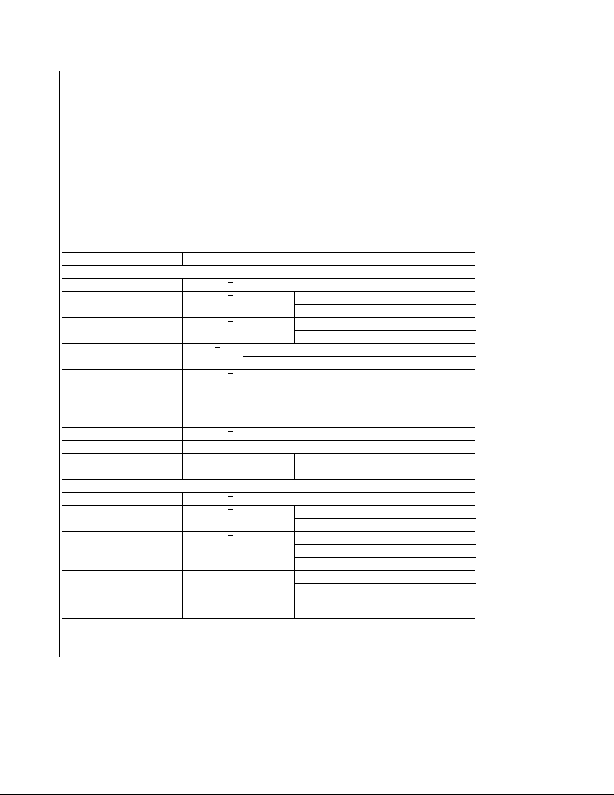
Symbol Parameter Conditions Min Typ Max Units
A PORT (A0–A7)
V
V
V
V
I
I
I
I
V
I
B PORT (B0–B7)
V
V
V
V
I
Logical ‘‘1’’ Input Voltage CDeVIL, T/Re2.0V 2.0 V
IH
Logical ‘‘0’’ Input Voltage CDeVIL, T/Re2.0V DP8304B 0.8 V
IL
DP7304B 0.7 V
Logical ‘‘1’’ Output Voltage CDeVIL, T/ReV
OH
Logical ‘‘0’’ Output Voltage CDeT/ReVILI
OL
Output Short Circuit CDeVIL, T/ReVIL,V
OS
Current V
Logical ‘‘1’’ Input Current CDeVIL, T/Re2.0V, V
IH
Input Current at Maximum CDe2.0V, V
I
Input Voltage
Logical ‘‘0’’ Input Current CDeVIL, T/Re2.0V, V
IL
Input Clamp Voltage CDe2.0V, I
CLAMP
Output/Input CDe2.0V V
OD
TRI-STATE Current
Logical ‘‘1’’ Input Voltage CDeVIL, T/ReV
IH
Logical ‘‘0’’ Input Voltage CDeVIL, T/ReV
IL
CC
e
Max (Note 4)
CC
eb
IN
eb
I
IL
e
16 mA (8304B) 0.35 0.5 V
OL
e
I
8 mA (both) 0.3 0.4 V
OL
e
0V,
O
e
2.7V 0.1 80 mA
IH
e
Max, V
e
5.25V
IH
e
0.4V
IN
0.4 mA V
OH
eb
I
3 mA 2.7 3.95 V
OH
12 mA
e
0.4V
IN
e
V
4.0V 80 mA
IN
IL
IL
DP8304B 0.8 V
b
1.15 V
CC
b
CC
10
2.0 V
DP7304B 0.7 V
Logical ‘‘1’’ Output Voltage CDeVIL, T/Re2.0V I
OH
Logical ‘‘0’’ Output Voltage CDeVIL, T/Re2.0V I
OL
Output Short Circuit CDeVIL, T/Re2.0V, V
OS
Current V
CC
e
Max (Note 4)
eb
0.4 mA V
OH
eb
I
5 mA 2.7 3.9 V
OH
eb
I
10 mA 2.4 3.6 V
OH
e
20 mA 0.3 0.4 V
OL
e
I
48 mA 0.4 0.5 V
OL
e
0V,
O
CC
b
b
1.15 V
25
CC
b
0.7 V
b
38
b
b
70
b
b
0.7
b
b
0.8 V
b
b
50
b
75 mA
1mA
200 mA
1.5 V
200 mA
150 mA
http://www.national.com 2
Page 3

DC Electrical Characteristics (Notes 2 and 3) (Continued)
Symbol Parameter Conditions Min Typ Max Units
B PORT (B0–B7) (Continued)
I
IH
I
I
I
IL
V
CLAMP
I
OD
Logical ‘‘1’’ Input Current CDeVIL, T/ReVIL,V
Input Current at Maximum CDe2.0V, V
Input Voltage
Logical ‘‘0’’ Input Current CDeVIL, T/ReVIL,V
Input Clamp Voltage CDe2.0V, I
Output/Input CDe2.0V V
TRI-STATE Current
CONTROL INPUTS CD, T/R
V
IH
V
IL
I
IH
I
I
I
IL
V
CLAMP
Logical ‘‘1’’ Input Voltage 2.0 V
Logical ‘‘0’’ Input Voltage DP8304B 0.8 V
Logical ‘‘1’’ Input Current V
Maximum Input Current V
Logical ‘‘0’’ Input Current V
Input Clamp Voltage I
POWER SUPPLY CURRENT
I
CC
Power Supply Current CDe2.0V, V
CC
eb
IN
e
2.7V 0.5 20 mA
IH
e
Max, V
CC
e
IL
eb
IN
CDeV
IH
0.4V T/R
12 mA
e
IN
e
0.4V, T/Re2V, V
INA
e
2.7V 0.1 80 mA
IH
e
Max, V
IN
12 mA
e
5.25V
IH
e
0.4V
e
0.4V
IN
e
V
4.0V
IN
b
70
b
0.7
1mA
b
200 mA
b
1.5 V
b
200 mA
a
200 mA
DP7304B 0.7 V
e
5.25V 1.0 mA
0.4V, V
b
CD
e
Max 70 100 mA
CC
e
Max 90 140 mA
CC
b
b
0.1
0.25
0.8
b
0.25 mA
b
0.5 mA
b
1.5 V
AC Electrical Characteristics V
CC
e
5V, T
e
25§C
A
Symbol Parameter Conditions Min Typ Max Units
A PORT DATA/MODE SPECIFICATIONS
t
PDHLA
t
PDLHA
t
PLZA
t
PHZA
t
PZLA
t
PZHA
Propagation Delay to a Logical ‘‘0’’ from CDe0.4V, T/Re0.4V
e
B Port to A Port R1
1k, R2e5k, C1e30 pF
Propagation Delay to a Logical ‘‘1’’ from CDe0.4V, T/Re0.4V
e
B Port to A Port R1
1k, R2e5k, C1e30 pF
(Figure A)
(Figure A)
Propagation Delay from a Logical ‘‘0’’ to B0 to B7e0.4V, T/Re0.4V
e
TRI-STATE from CD to A Port S3
1, R5e1k, C4e15 pF
Propagation Delay from a Logical ‘‘1’’ to B0 to B7e2.4V, T/Re0.4V
e
TRI-STATE from CD to A Port S3
0, R5e1k, CRe15 pF
Propagation Delay from TRI-STATE to B0 to B7e0.4V, T/Re0.4V
e
a Logical ‘‘0’’ from CD to A Port S3
1, R5e1k, C4e30 pF
Propagation Delay from TRI-STATE to B0 to B7e2.4V, T/Re0.4V
e
a Logical ‘‘1’’ from CD to A Port S3
0, R5e5k, C4e30 pF
(Figure C)
(Figure C)
(Figure C)
(Figure C)
14 18 ns
13 18 ns
11 15 ns
815ns
27 35 ns
19 25 ns
B PORT DATA/MODE SPECIFICATIONS
t
PDHLB
t
PDLHB
Propagation Delay to a Logical ‘‘0’’ from CDe0.4V, T/Re2.4V
(Figure A)
A Port to B Port R1e100X,R2e1k, C1e300 pF 18 23 ns
e
R1
667X,R2e5k, C1e45 pF 11 18 ns
Propagation Delay to a Logical ‘‘1’’ from CDe0.4V, T/Re2.4V
(Figure A)
A Port to B Port R1e100X,R2e1k, C1e300 pF 16 23 ns
e
R1
667X,R2e5k, C1e45 pF 11 18 ns
http://www.national.com3
Page 4

AC Electrical Characteristics V
CC
e
5V, T
e
25§C (Continued)
A
Symbol Parameter Conditions Min Typ Max Units
B PORT DATA/MODE SPECIFICATIONS (Continued)
t
PLZB
t
PHZB
t
PZLB
Propagation Delay from a Logical ‘‘0’’ to A0 to A7e0.4V, T/Re2.4V
e
TRI-STATE from CD to B Port S3
1, R5e1k, C4e15 pF
Propagation Delay from a Logical ‘‘1’’ to A0 to A7e2.4V, T/Re2.4V
e
TRI-STATE from CD to B Port S3
0, R5e1k, C4e15 pF
Propagation Delay from TRI-STATE to A0 to A7e0.4V, T/Re2.4V
(Figure C)
(Figure C)
(Figure C)
13 18 ns
815 ns
a Logical ‘‘0’’ from CD to B Port S3e1, R5e100X,C4e300 pF 32 40 ns
S3e1, R5e667X,C4e45 pF 16 22 ns
t
PZHB
Propagation Delay from TRI-STATE to A0 to A7e2.4V, T/Re2.4V
(Figure C)
a Logical ‘‘1’’ from CD to B Port S3e0, R5e1k, C4e300 pF 26 35 ns
e
S3
0, R5e5k, C4e45 pF 14 22 ns
TRANSMIT/RECEIVE MODE SPECIFICATIONS
t
TRL
t
TRH
t
RTH
Note 1: ‘‘Absolute Maximum Ratings’’ are those values beyond which the safety of the device cannot be guaranteed. They are not meant to imply that the devices
should be operated at these limits. The tables of ‘‘Electrical Characteristics’’ provide conditions for actual device operation.
Note 2: Unless otherwise specified, min/max limits apply across the supply and temperature range listed in the table of Recommended Operating Conditions. All
typical values given are for V
Note 3: All currents into device pins are positive; all currents out of device pins are negative. All voltages are referenced to ground unless otherwise specified.
Note 4: Only one output at a time should be shorted.
Propagation Delay from Transmit Mode to CDe0.4V
(Figure B)
Receive a Logical ‘‘0’’, T/R to A Port S1e0, R4e100X,C3e5pF 30 40 ns
e
S2
1, R3e1k, C2e30 pF
Propagation Delay from Transmit Mode to CDe0.4V,
(Figure B)
Receive a Logical ‘‘1’’, T/R to A Port S1e1, R4e100X,C3e5pF 28 40 ns
e
S2
0, R3e5k, C2e30 pF
Propagation Delay from Receive Mode to CDe0.4V
(Figure B)
Transmit a Logical ‘’1’’, T/R to B Port S1e0, R4e1k, C3e300 pF 28 40 ns
e
S2
1, R3e300X,C2e5pF
e
CC
5V and T
e
25§C.
A
Switching Time Waveforms and AC Test Circuits
Note: C1 includes test fixture capacitance.
FIGURE A. Propagation Delay from A Port to B Port or from B Port to A Port
http://www.national.com 4
TL/F/8793– 3
TL/F/8793– 4
Page 5

Switching Time Waveforms and AC Test Circuits (Continued)
TL/F/8793– 5
Note: C2 and C3 include test fixture capacitance.
FIGURE B. Propagation Delay from T/R to A Port or B Port
Note: C4 includes test fixture capacitance.
Port input is in a fixed logical
condition. See AC table.
FIGURE C. Propagation Delay to/from TRI-STATE from CD to A Port or B Port
TL/F/8793– 6
TL/F/8793– 7
TL/F/8793– 8
http://www.national.com5
Page 6

http://www.national.com 6
Page 7

Physical Dimensions inches (millimeters)
Ceramic Dual-In-Line Package (J)
Order Number DP7304BJ or DP8304BJ
NS Package Number J20A
SO Package (M)
Order Number DP8304BWM
NS Package Number M20B
http://www.national.com7
Page 8

Physical Dimensions inches (millimeters) (Continued)
Molded Dual-In-Line Package (N)
Order Number DP8304BN
NS Package Number N20A
LIFE SUPPORT POLICY
NATIONAL’S PRODUCTS ARE NOT AUTHORIZED FOR USE AS CRITICAL COMPONENTS IN LIFE SUPPORT
DEVICES OR SYSTEMS WITHOUT THE EXPRESS WRITTEN APPROVAL OF THE PRESIDENT OF NATIONAL
SEMICONDUCTOR CORPORATION. As used herein:
1. Life support devices or systems are devices or 2. A critical component is any component of a life
DP7304B/DP8304B 8-Bit TRI-STATE Bidirectional Transceiver (Non-Inverting)
systems which, (a) are intended for surgical implant support device or system whose failure to perform can
into the body, or (b) support or sustain life, and whose be reasonably expected to cause the failure of the life
failure to perform, when properly used in accordance support device or system, or to affect its safety or
with instructions for use provided in the labeling, can effectiveness.
be reasonably expected to result in a significant injury
to the user.
National Semiconductor National Semiconductor National Semiconductor National Semiconductor
Corporation Europe Hong Kong Ltd. Japan Ltd.
1111 West Bardin Road Fax:
Arlington, TX 76017 Email: europe.support@nsc.com Ocean Centre, 5 Canton Rd. Fax: 81-043-299-2408
Tel: 1(800) 272-9959 Deutsch Tel:
Fax: 1(800) 737-7018 English Tel:
http://www.national.com
National does not assume any responsibility for use of any circuitry described, no circuit patent licenses are implied and National reserves the right at any time without notice to change said circuitry and specifications.
Fran3ais Tel:
Italiano Tel:a49 (0) 180-534 16 80 Fax: (852) 2736-9960
a
49 (0) 180-530 85 86 13th Floor, Straight Block, Tel: 81-043-299-2308
a
49 (0) 180-530 85 85 Tsimshatsui, Kowloon
a
49 (0) 180-532 78 32 Hong Kong
a
49 (0) 180-532 93 58 Tel: (852) 2737-1600
 Loading...