

Page 1
TL/F/6825
DP8228/DP8228M/DP8238/DP8238M System Controller and Bus Driver
December 1988
DP8228/DP8228M/DP8238/DP8238M
System Controller and Bus Driver
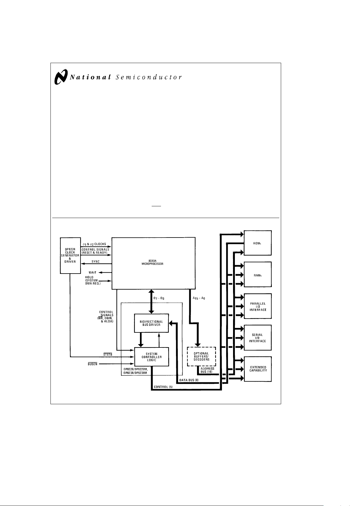
General Description
The DP8228/DP8228M, DP8238/DP8238M are system
controller/bus drivers contained in a standard, 28-pin dualin-line package. The chip, which is fabricated using Schottky
Bipolar technology, generates all the read and write control
signals required to directly interface the memory and input/
output components of the 8080A microcomputer family. The
chip also provides drive and isolation for the bidirectional
data bus of the 8080A microprocessor. Data bus isolation
enables the use of slower memory and input/output components in a system, and provides for enhanced system noise
immunity.
A user-selected signal-level interrupt vector (RST 7) is provided by the device for use in the interrupt structure of small
systems that need only one basic vector. No additional
components (such as an interrupt instruction port) are required to use the single interrupt vector in these systems.
The devices also generate an Interrupt Acknowledge (INTA
)
control signal for each byte of a multibyte CALL instruction
when an interrupt is acknowledged by the 8080A. This feature permits the use of a multilevel priority interrupt structure
in large, interrupt-driven systems.
Features
Y
Single chip system controller and bus driver for 8080A
Microcomputer Systems
Y
Allows use of multibyte CALL instructions for Interrupt
Acknowledge
Y
Provides user-selected single-level interrupt vector
(RST 7)
Y
Provides isolation of data bus
Y
Supports a wide variety of system bus structures
Y
Reduces system component count
Y
DP8238/DP8238M provides advanced Input/Output
Write and Memory Write control signals for large system timing control
8080A Microcomputer Family Block Diagram
TL/F/6825– 1
TRI-STATEÉis a registered trademark of National Semiconductor Corporation.
C
1995 National Semiconductor Corporation RRD-B30M105/Printed in U. S. A.
Page 2
Absolute Maximum Ratings
If Military/Aerospace specified devices are required,
please contact the National Semiconductor Sales
Office/Distributors for availability and specifications.
Storage Temperature
b
65§Ctoa150§C
Supply Voltage, V
CC
b
0.5 toa7V
Input Voltage
b
1.5V toa7V
Output Current 100 mA
Maximum Power Dissipation* at 25§C
Cavity Package 2179 mW
Molded Package 2361 mW
*Derate cavity package 14.5 mW/§C above 25§C; derate molded package
18.9 mW/
§
C above 25§C.
Operating Conditions
Min Max Units
Supply Voltage (V
CC
)
DP8228M, DP8238M 4.50 5.50 V
DC
DP8228, DP8238 4.75 5.25 V
DC
Operating Temperature (TA)
DP8228M, DP8238M
b
55
a
125
§
C
DP8228, DP8238 0
a
70
§
C
Note:
Maximum ratings indicate limits beyond which permanent damage may occur. Continuous operation at these limits is not intended and should be limited to those conditions
specified under DC electrical characteristics.
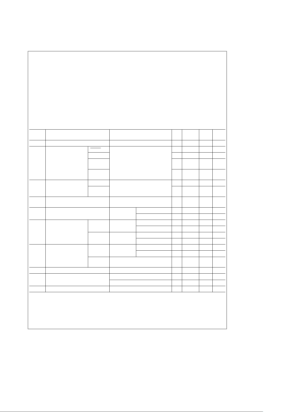
Electrical Characteristics Min
s
T
A
s
Max, MinsV
CC
s
Max, unless otherwise noted
Symbol Parameter Conditions Min
Typ
Max Units
(Note 1)
V
C
Input Clamp Voltage, All Inputs V
CC
e
Min, I
C
eb
5 mA 0.6
b
1.0 V
I
F
Input Load STSTB V
CC
e
Max 500 mA
Current
D2 and D6
V
F
e
0.45V for DP8228, DP8238
750 mA
D0, D1, D4,
V
F
e
0.40V for DP8228M, DP8238M
250 mA
D5 and D7
All Other
250 mA
Inputs
I
R
Input Leakage DB0–DB7 V
CC
e
Max, V
R
e
V
CC
20 mA
Current
All Other
100 mA
Inputs
V
TH
Input Threshold Voltage, V
CC
e
5V
0.8 2.0 V
All Inputs
I
CC
Power Supply Current V
CC
e
Max DP8228, DP8238 185 230 mA
DP8228M, DP8238M 160 230 mA
V
OL
Output Low D0–D7 V
CC
e
Min, DP8228M, DP8238M 0.50 V
Voltage I
OL
e
2mA
DP8228, DP8238 0.45 V
All Other V
CC
e
Min, DP8228M, DP8238M 0.50 V
Outputs I
OL
e
10 mA
DP8228, DP8238 0.45 V
V
OH
Output High D0– D7 V
C
e
Min, DP8228M, DP8238M 3.3 3.8 V
I
OL
eb
10 mA
DP8228, DP8238 3.6 3.8 V
All Other V
CC
e
Min, I
OH
eb
1mA
2.4 3.8 V
Outputs
I
OS
Short Circuit Current, All Outputs V
CC
e
5V, V
O
e
0V 15 90 mA
I
O (OFF)
OFF State Output Current V
CC
e
Max, V
O
e
V
CC
100 mA
All Control Outputs
V
CC
e
Max, V
O
e
0.45V
b
100 mA
I
INT
INTA Current (See Test Conditions,
Figure 3
)5mA
Note 1: Typical values are for T
A
e
25§C and typical supply voltages.
2
Page 3

Capacitance* V
BIAS
e
2.5V, V
CC
e
5.0V, T
A
e
25§C, fe1 MHz
Symbol Parameter Min
Typ
Max Units
(Note 1)
C
IN
Input Capacitance 8 12 pF
C
OUT
Output Capacitance Control Signals 7 15 pF
I/O I/O Capacitance (D or DB) 8 15 pF
*This parameter is periodically sampled and not 100% tested.
Switching Characteristics Min
s
V
CC
s
Max, MinsT
A
s
Max
DP8228M, DP8228,
Symbol Parameter Conditions DP8238M DP8238 Units
Min Max Min Max
t
PW
Width of Status Strobe 25 22 ns
t
SS
Set-Up Time, Status Inputs D0–D7 8 8 ns
t
SH
Hold Time, Status Inuts D0–D7 5 5 ns
t
DC
Delay from STSTB to Any Control Signal
(Figure 2)
20 75 20 60 ns
t
RR
Delay from DBIN to Control Outputs
(Figure 2)
30 30 ns
t
RE
Delay from DBIN to Enable/
(Figure 1)
45 45 ns
Disable 8080 Bus
t
RD
Delay from System Bus to 8080
(Figure 1)
45 30 ns
Bus During Read
t
WR
Delay from WR to Control Outputs
(Figure 2)
560545 ns
tWEDelay to Enable System Bus
(Figure 2)
30 30 ns
DB0–DB7 after STSTB
t
WD
Delay from 8080 Bus D0–D7 to
(Figure 2)
540540 ns
System Bus DB0–DB7 During Write
t
E
Delay from System Bus Enable to
(Figure 2)
30 30 ns
System Bus DB0–DB7
t
HD
HLDA to Read Status Outputs
(Figure 2)
25 25 ns
t
DS
Set-Up Time, System Bus Inputs to HLDA 10 10 ns
t
DH
Hold Time, System Bus Inputs to HLDA 20 20 ns
Test Conditions
TL/F/6825– 2
TL/F/6825– 3
TL/F/6825– 4
FIGURE 1. Test Load FIGURE 2. Test Load FIGURE 3. INTA Test Circuit
(For RST 7)
3
Page 4

Timing Diagram
TL/F/6825– 5
VOLTAGE MEASUREMENT POINTS: D0–D7(when outputs) Logic ‘‘0’’e0.8V, Logic ‘‘0’’e0.8V, Logic ‘‘1’’e3.0V. All other signals measured at 1.5V.
*Advanced I/OW
MEMW for 8238 only.
Functional Pin Definitions
The following describes the function of all of the DP8228/
DP8228M, DP8238/DP8238M pinouts. Some of these descriptions reference internal circuits.
INPUT SIGNALS
Status Strobe (STSTB
): Activated (low) at the start of each
new machine cycle. The STSTB
input is used to store a
status word (refer to chart) from the 8080A microprocessor
into the internal status latch of the DP8228, DP8238. The
status word is latched when the STSTB
returns to the high
state. The 8080A outputs this status word onto its data bus
during the first state (SYNC interval) of each machine cycle.
Data Bus In (DBIN): When high, indicates that the 8080A
data bus is in the input mode. The DBIN signal is used to
gate data from memory or an input/output device onto the
data bus.
Write (WR
): When low, indicates that the data on the
8080A data bus are stable for WRITE memory or output
operation.
Hold Acknowledge (HLDA): When high, indicates that the
8080A data and address buses will go to their high impedance state. When in the data bus read mode, DBIN input in
the high state, a high HLDA input will latch the data bus
information into the driver circuits and gate off the applicable control signal I/OR
, MEMR, or INTA (return to the out-
put high state).
Bus Enable (BUSEN
): Asynchronous DMA input to the in-
ternal gating array. When low, normal operation of the internal bidirectional bus driver and gating array occurs. When
high, the bus driver and gating array are driven to their high
impedance state.
V
CC
Supply:a5V.
Ground: 0V reference.
OUTPUT SIGNALS
Memory Read (MEMR
): When low, signals data to be load-
ed in from memory. The MEMR
signal is generated by strob-
ing in status word 1, 2, or 4. (Refer to status word chart.)
Memory Write (MEMW
): When low, signals data to be
stored in memory. The MEMW
signal is generated for the
DP8238 by strobing in status word 3 or 5. (Refer to status
word chart.) For the DP8228, the MEMW
signal is generated
by gating a low-level WR
input with the strobed in status
word3or5.
Input/Output Read (I/OR
): When low, signals data to be
loaded in from an addressed input/output device. The I/OR
signal is generated by strobing in status word 6.
Input/Output Write (I/OW
): When low, signals data to be
transferred to an addressed input/output device. The I/OW
signal for the DP8238 is generated by strobing in status
word 7. For the DP8238 the I/OW
signal is generated by
gating in a low-level WR
input with the strobed in status
word 7.
Interrupt Acknowledge (INTA
): When low, indicates that
an interrupt has been acknowledged by the 8080A microprocessor. The INTA
signal is generated by strobing in
staus word 8 or 10.
Signal Level Interrupt (RST 7): When the INTA
output is
tied to 12V througha1kXresistor, strobing in status word 8
or 10 will cause the CPU data bus outputs, when active, to
go to the high state.
INPUT/OUTPUT SIGNALS
CPU Data (D
7–D0
) Bus: This bus comprises eight
TRI-STATE
É
input/output lines that connect to the 8080A
microprocessor. The bus provides bidirectional communica-
4
Page 5

Functional Pin Definitions (Continued)
tion between the CPU, memory, and input/output devices
for instructions and data transfers. A status word (which describes the current machine cycle) is also outputted on this
data bus during the first microcycle of each machine cycle
(SYNC
e
logic 1).
System Data (DB
7
–DB0) Bus: This bus comprises eight
TRI-STATE input/output lines that connect to the memory
and input/output components of the system. The internal
bidirectional bus driver isolates the DB
7
–DB0Data Bus from
the D
7–D0
Data Bus.
Status Word Chart
Machine Cycle
Status Data Bus Bit Control
Word
D7D6D5D4D3D2D1D
0
Signal
Instruction Fetch 1 1 0 1 0 0 0 1 0 MEMR
Memory Read 2 1 0 0 0 0 0 1 0 MEMR
Memory Write 3 0 0 0 0 0 0 0 0 MEMW
Stack Read 4 1 0 0 0 0 1 1 0 MEMR
Stack Write 5 0 0 0 0 0 1 0 0 MEMW
Input Read 6 0 1 0 0 0 0 1 0 I/OR
Output Write 7 0 0 0 1 0 0 0 0 I/OW
Interrupt Acknowledge 8 0 0 1 0 0 0 1 1 INTA
Halt Acknowledge 9 1 0 0 0 1 0 1 0 (none)
Interrupt Acknowledge While Halt 10 0 0 1 0 1 0 1 1 INTA
Block and Connection Diagrams
TL/F/6825– 6
Dual-In-Line Package
TL/F/6825– 7
Order Number DP8228J, DP8228MJ,
DP8228N, DP8238J, DP8238MJ or
DP8238N
See NS Package Number J28A or N28B
5
Page 6

DP8228/DP8228M/DP8238/DP8238M System Controller and Bus Driver
Physical Dimensions inches (millimeters)
Ceramic Dual-In-Line Package (J)
Order Number DP8228J, DP8228MJ, DP8238J or DP8238MJ
NS Package Number J28A
Molded Dual-In-Line Package (N)
Order Number DP8228N or DP8238N
NS Package Number N28B
LIFE SUPPORT POLICY
NATIONAL’S PRODUCTS ARE NOT AUTHORIZED FOR USE AS CRITICAL COMPONENTS IN LIFE SUPPORT
DEVICES OR SYSTEMS WITHOUT THE EXPRESS WRITTEN APPROVAL OF THE PRESIDENT OF NATIONAL
SEMICONDUCTOR CORPORATION. As used herein:
1. Life support devices or systems are devices or 2. A critical component is any component of a life
systems which, (a) are intended for surgical implant support device or system whose failure to perform can
into the body, or (b) support or sustain life, and whose be reasonably expected to cause the failure of the life
failure to perform, when properly used in accordance support device or system, or to affect its safety or
with instructions for use provided in the labeling, can effectiveness.
be reasonably expected to result in a significant injury
to the user.
National Semiconductor National Semiconductor National Semiconductor National Semiconductor
Corporation Europe Hong Kong Ltd. Japan Ltd.
1111 West Bardin Road Fax: (
a
49) 0-180-530 85 86 13th Floor, Straight Block, Tel: 81-043-299-2309
Arlington, TX 76017 Email: cnjwge@tevm2.nsc.com Ocean Centre, 5 Canton Rd. Fax: 81-043-299-2408
Tel: 1(800) 272-9959 Deutsch Tel: (
a
49) 0-180-530 85 85 Tsimshatsui, Kowloon
Fax: 1(800) 737-7018 English Tel: (
a
49) 0-180-532 78 32 Hong Kong
Fran3ais Tel: (
a
49) 0-180-532 93 58 Tel: (852) 2737-1600
Italiano Tel: (
a
49) 0-180-534 16 80 Fax: (852) 2736-9960
National does not assume any responsibility for use of any circuitry described, no circuit patent licenses are implied and National reserves the right at any time without notice to change said circuitry and specifications.
 Loading...