

Page 1
DP8224 Clock Generator and Driver
DP8224 Clock Generator and Driver
June 1986
General Description
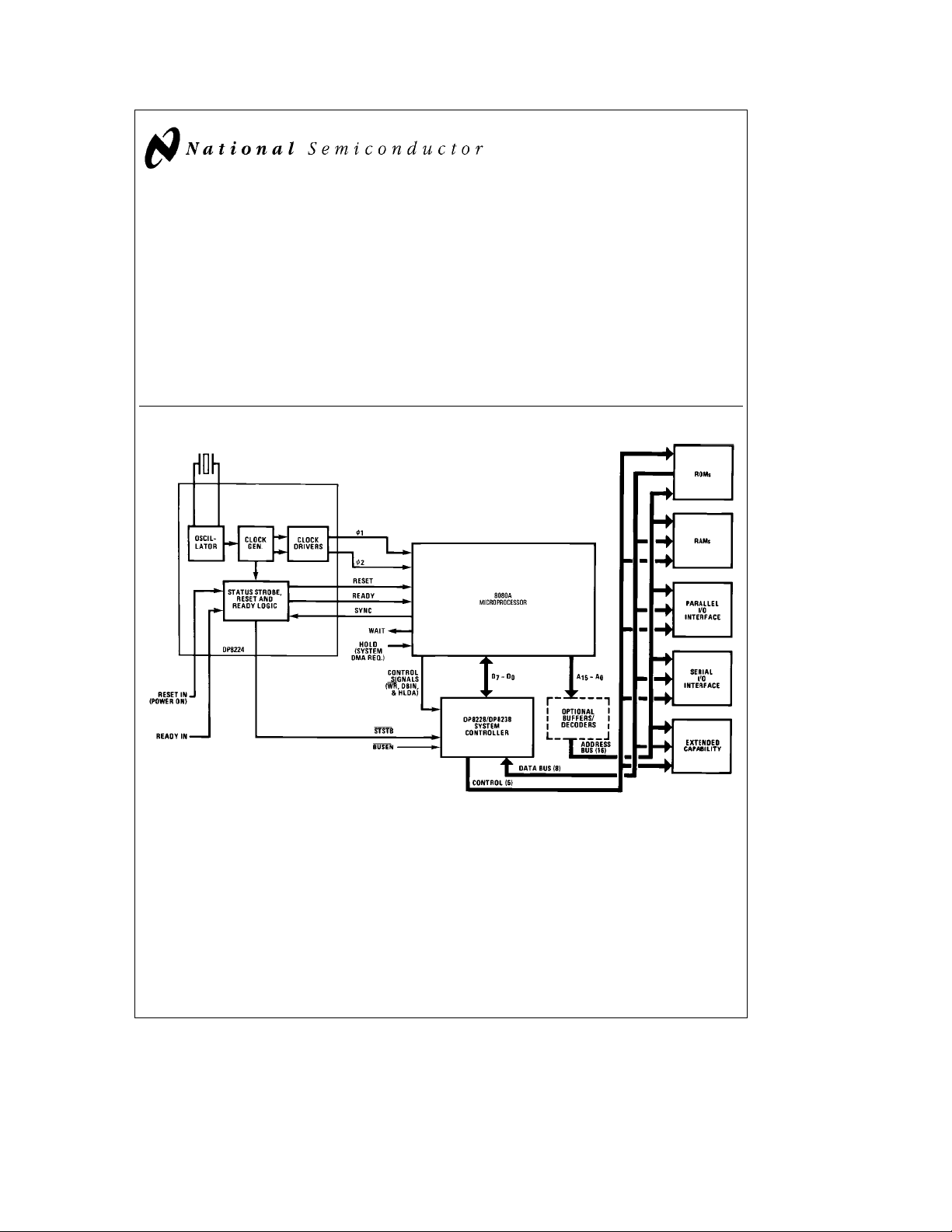
The DP8224 is a clock generator/driver contained in a standard, 16-pin dual-in-line package. The chip, which is fabricated using Schottky Bipolar technology, generates clocks
and timing for the 8080A microcomputer family.
Included in the DP8224 is an oscillator circuit that is controlled by an external crystal, which is selected by the designer to meet a variety of system speed requirements. Also
included in the chip are circuits that provide: a status strobe
for the DP8228 or DP8238 system controllers, power-on reset for the 8080A microprocessor, and synchronization of
the READY input to the 8080A.
Features
Y
Crystal-controlled oscillator for stable system operation
Y
Single chip clock generator and driver for 8080A microprocessor
Y
Provides status strobe for DP8228 or DP8238 system
controllers
Y
Provides power-on reset for 8080A microprocessor
Y
Synchronizes READY input to 8080A microprocessor
Y
Provides oscillator output for synchronization of external circuits
Y
Reduces system component count
8080A Microcomputer Family Block Diagram
TL/F/8752– 1
C
1995 National Semiconductor Corporation RRD-B30M105/Printed in U. S. A.
TL/F/8752
Page 2
Absolute Maximum Ratings (Note 2)
If Military/Aerospace specified devices are required,
please contact the National Semiconductor Sales
Office/Distributors for availability and specifications.
Supply Voltage
V
CC
V
DD
Input Voltage
Storage Temperature Range
b
1V toa5.5V
b
65§Ctoa150§C
7V
15V
Operating Conditions
Supply Voltage
V
CC
V
DD
Temperature (T
)0
A
Min Max Units
4.75 5.25 V
11.4 12.6 V
a
70
C
§
Maximum Power Dissipation* at 25§C
Cavity Package 1509 mW
Molded Package 1476 mW
Lead Temperature (Soldering, 4 seconds) 260
* Derate cavity package 10.1 mW/§C above 25§C; derate molded package
11.8 mW/
C above 25§C.
§
C
§
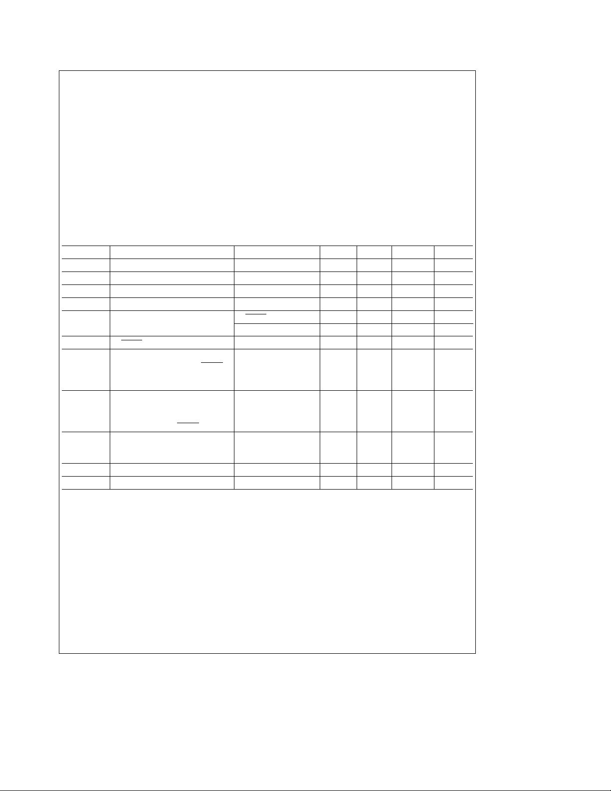
Electrical Characteristics (Note 3)
Symbol Parameter Conditions Min Typ Max Units
I
F
I
R
V
C
V
IL
V
IH
Input Current Loading V
Input Leakage Current V
Input Forward Clamp Voltage I
Input ‘‘Low’’ Voltage V
Input ‘‘High’’ Voltage RESIN Input 2.6 V
e
0.45V
F
e
5.25V 10 mA
R
eb
5mA
C
e
5V 0.8 V
CC
All Other Inputs 2.0 V
b
V
V
IH
V
OL
RESIN Input Hysteresis V
IL
Output ‘‘Low’’ Voltage
(w1, w2), Ready, Reset STSTB
Osc., w2 (TTL) I
Osc., w2 (TTL) I
V
OH
Output ‘‘High’’ Voltage
w1, w2I
Ready, Reset I
Osc., w2 (TTL), STSTB
I
SC
Output Short-Circuit Current V
(All Low Voltage Outputs Only),
e
5V 0.25 V
CC
e
I
2.5 mA 0.45 V
OL
e
10 mA 0.45 V
OL
e
15 mA 0.45 V
OL
eb
100 mA 9.4 V
OH
eb
100 mA 3.6 V
OH
eb
I
1 mA 2.4 V
OH
e
O
0V, V
CC
e
5V
b
10
(Note 1)
I
CC
I
DD
Note 1: Cautionbw1 and w2 output drivers do not have short circuit protection.
Note 2: ‘‘Absolute Maximum Ratings’’ are those values beyond which the safety of the device cannot be guaranteed. Except for ‘‘Operating Temperature Range’’
they are not meant to imply that the devices should be operated at these limits. The table of ‘‘Electrical Characteristics’’ provides conditions for actual device
operation.
Note 3: Unless otherwise specified min/max limits apply across the 0
e
12V.
V
DD
Power Supply Current 115 mA
Power Supply Current 12 mA
Ctoa70§C range for the DP8224. All typical values are for T
§
b
0.25 mA
b
1.0 V
b
60 mA
e
25§C, V
A
e
5V, and
CC
Crystal Requirements*
Tolerance 0.005% at 0§Ctoa70§C
Resonance Fundamental
Load Capacitance 20 pF to 30 pF
*It is good design practice to ground the case of the crystal
**With tank circuit, use 3rd overtone mode
Equivalent Resistance 75X to 20X
Power Dissipation (Min) 4 mW
2
Page 3
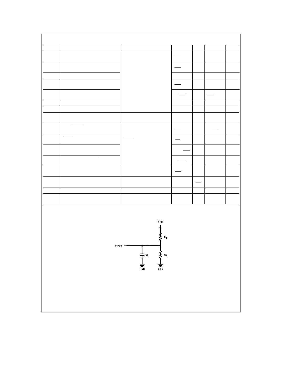
Switching Characteristics (Note 3)
Symbol Parameter Conditions Min Typ Max Units
t
w1
t
w2
t
D1
t
D2
t
D3
t
r
t
f
t
Dw2
t
DSS
t
PW
t
DRS
t
DRH
t
DR
t
CLK
f
MAX
C
IN
w1 Pulse Width
w2 Pulse Width
w1tow2 Delay
w2tow1 Delay
w1tow2 Delay
w1 and w2 Rise Time 20 ns
w1 and w2 Fall Time 20 ns
w2tow2 (TTL) Delay w2 TTL, C
w2 to STSTB Delay
STSTB Pulse Width
RDYIN Set-Up Time to Status Strobe
RDYIN Hold Time After STSTB
READY or RESET to w2 Delay Ready and Reset, C
CLK Period
Maximum Oscillating Frequency 27 MHz
Input Capacitance V
e
C
20 pF to 50 pF
L
e
30 pF,
L
e
300X,R2e600X
R1
,C
e
15 pF
L
STSTB
R1e2kX,R2e4kX
DD
L
e
12V,
e
2kX,R2e4kX
R1
e
5V, V
CC
e
V
BIAS
2.5V, fe1 MHz
e
10 pF,
2t
CY
b
20 ns
9
5t
CY
b
35 ns
9
0ns
2t
CY
b
14 ns
9
2t
CY
9
b
515ns
6t
CY
b
30
9
t
CY
b
15 ns
9
4t
CY
b
50
9
4t
CY
9
4t
CY
b
25 ns
9
2t
CY
a
20 ns
9
6t
CY
9
ns
ns
ns
t
CY
9
ns
8pF
Test Circuit
TL/F/8752– 2
3
Page 4

Waveforms
Voltage Measurement Points: w1, w 2 Logic ‘‘0’’e1.0V, Logic ‘‘1’’e8.0V. All other signals measured at 1.5V.
Switching Characteristics (For t
CY
e
488.28 ns)
TL/F/8752– 3
Symbol Parameter Conditions Min Typ Max Units
t
w1
t
w2
t
D1
t
D2
t
D3
t
r
t
f
t
DSS
t
Dw2
w1 Pulse Width 89 ns
w2 Pulse Width 236 ns
Delay w1tow20ns
Delay w2tow195ns
Delay w1tow2 Leading Edges 109 129 ns
Output Rise Time
Output Fall Time
w2 to STSTB Delay
w2tow2 (TTL) Delay
w1 and w2 Loaded to C
Ready and Reset Loaded to 2 mA/10 pF
e
L
20 to 50 pF
All Measurements Referenced to 1.5V
unless Specified Otherwise
296 326 ns
b
515ns
20 ns
20 ns
tPWStatus Strobe Pulse Width 40 ns
t
DRS
t
DRH
t
DR
f
MAX
RDYIN Set-Up Time to STSTB
RDYIN Hold Time after STSTB 217 ns
READY or RESET to w2 Delay 192 ns
Oscillator Frequency 18.432 MHz
b
167 ns
4
Page 5

Functional Pin Definitions
The following describes the function of all of the DP8224
input/output pins. Some of these descriptions reference internal circuits.
INPUT SIGNALS
Crystal Connections (XTAL 1 and XTAL 2): Two inputs
that connect an external crystal to the oscillator circuit of
the DP8224. Normally, a fundamental mode crystal is used
to determine the basic operating frequency of the oscillator.
However, overtone mode crystals may also be used. The
crystal frequency is 9 times the desired microprocessor
speed (that is, crystal frequency equals 1/t
the crystal frequency is above 10 MHz, a selected capacitor
(3 to 10 pF) may have to be connected in series with the
crystal to produce the exact desired frequency.
Tank: Allows the use of overtone mode crystals with the
oscillator circuit. When an overtone mode crystal is used,
the tank input connects to a parallel LC network that is ac
coupled to ground. The formula for determining the resonant frequency of this LC network is as follows:
1
e
F
2q0LC
Synchronizing (SYNC) Signal: When high, indicates the
beginning of a new machine cycle. The 8080A microprocessor outputs a status word (which describes the current machine cycle) onto its data bus during the first state (SYNC
interval) of each machine cycle.
Reset In (RESIN
): Provides an automatic system reset and
start-up upon application of power as follows. The RESIN
input, which is obtained from the junction of an external RC
network that is connected between V
ed to an internal Schmitt Trigger circuit. This circuit converts
CC
the slow transition of the power supply rise into a sharp,
clean edge when its input reaches a predetermined value.
When this occurs, an internal D-type flip-flop is synchronously reset, thereby providing the RESET output signal discussed below.
c
9). When
CY
Figure A
.
and ground, is rout-
For manual system reset, a momentary contact switch that
provides a low (ground) when closed is also connected to
the RESIN
input.
Ready In (RDYIN): An asynchronous READY signal that is
re-clocked by a D-type flip-flop of the DP8224 to provide the
synchronous READY output discussed below.
a
5 Volts: VCCsupply.
a
12 Volts: VDDsupply.
Ground: 0 volt reference.
OUTPUT SIGNALS
Oscillator (OSC): A buffered oscillator signal that can be
used for external timing purposes.
w
and w2Clocks: Two non-TTL compatible clock phases
1
that provide nonoverlapping timing references for internal
storage elements and logic circuits of the 8080A microprocessor. The two clock phases are produced by an internal
clock generator that consists of a divide-by-nine counter
and the associated decode gating logic.
Figure B
.
w2(TTL) Clock: A TTL w2clock phase that can be used for
external timing purposes.
Status Strobe (STSTB
new machine cycle. The STSTB
ing a high-level SYNC input with the w
the internal clock generator of the DP8224. The STSTB
): Activated (low) at the start of each
signal is generated by gat-
timing signal from
1A
signal is used to clock status information into the status latch
of the DP8228 system controller and bus driver.
Reset: When the RESET signal is activated, the content of
the program counter of the 8080A is cleared. After
RESET, the program will start at location 0 in memory.
Ready: The READY signal indicates to the 8080A that valid
memory or input data is available. This signal is used to
synchronize the 8080A with slower memory or input/output
devices.
Logic and Connection Diagrams
Dual-In-Line Package
TL/F/8752– 5
Top View
Order Number DP8224J or DP8224N
See NS Package Number
J16A or N16A
TL/F/8752– 4
5
Page 6

Applications Information
FIGURE A. DP8224 Connection Diagram
TL/F/8752– 6
EXAMPLE: (8080 t
CY
e
OSC
18 MHz/55 ns
e
w
110 ns (2c55 ns)
1
e
w
275 ns (5c55 ns)
2
e
w
2–w1
e
500 ns)
110 ns (2c55 ns)
FIGURE B. DP8224 Clock Generator Waveforms
TL/F/8752– 7
6
Page 7

Physical Dimensions inches (millimeters)
Ceramic Dual-In-Line Package (J)
Order Number DP8224J
NS Package Number J16A
7
Page 8

Physical Dimensions inches (millimeters) (Continued)
DP8224 Clock Generator and Driver
Molded Dual-In-Line Package (N)
Order Number DP8224N
NS Package Number N16A
LIFE SUPPORT POLICY
NATIONAL’S PRODUCTS ARE NOT AUTHORIZED FOR USE AS CRITICAL COMPONENTS IN LIFE SUPPORT
DEVICES OR SYSTEMS WITHOUT THE EXPRESS WRITTEN APPROVAL OF THE PRESIDENT OF NATIONAL
SEMICONDUCTOR CORPORATION. As used herein:
1. Life support devices or systems are devices or 2. A critical component is any component of a life
systems which, (a) are intended for surgical implant support device or system whose failure to perform can
into the body, or (b) support or sustain life, and whose be reasonably expected to cause the failure of the life
failure to perform, when properly used in accordance support device or system, or to affect its safety or
with instructions for use provided in the labeling, can effectiveness.
be reasonably expected to result in a significant injury
to the user.
National Semiconductor National Semiconductor National Semiconductor National Semiconductor
Corporation Europe Hong Kong Ltd. Japan Ltd.
1111 West Bardin Road Fax: (
Arlington, TX 76017 Email: cnjwge@tevm2.nsc.com Ocean Centre, 5 Canton Rd. Fax: 81-043-299-2408
Tel: 1(800) 272-9959 Deutsch Tel: (
Fax: 1(800) 737-7018 English Tel: (
National does not assume any responsibility for use of any circuitry described, no circuit patent licenses are implied and National reserves the right at any time without notice to change said circuitry and specifications.
Fran3ais Tel: (
Italiano Tel: (
a
49) 0-180-530 85 86 13th Floor, Straight Block, Tel: 81-043-299-2309
a
49) 0-180-530 85 85 Tsimshatsui, Kowloon
a
49) 0-180-532 78 32 Hong Kong
a
49) 0-180-532 93 58 Tel: (852) 2737-1600
a
49) 0-180-534 16 80 Fax: (852) 2736-9960
 Loading...