

Page 1
Hall ICs
DN6849UBS
Hall IC for alternative magnetic field
■ Overview
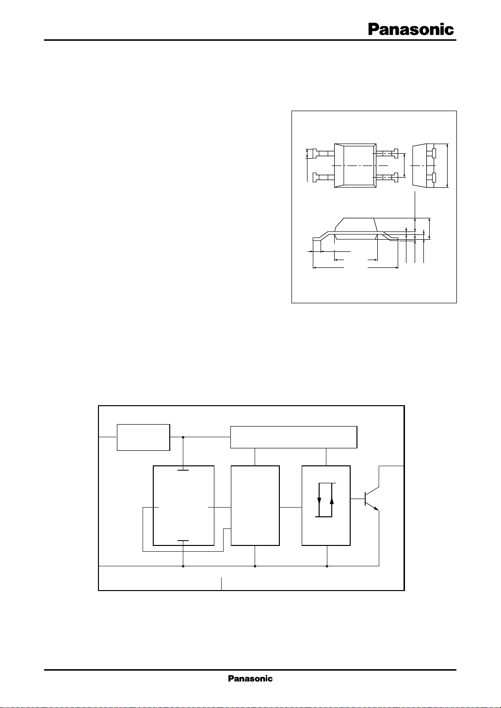
The DN6849UBS is a Hall IC in which a Hall element,
an amplifier circuit, Schmidt circuit, stabilized power supply and temperature compensation circuit are integrated
onto a single chip using IC technology. It amplifies Hall
element output in the amplifier, converts it into a digital
signal through the Schmidt circuit so as to drive the TTL
or MOS IC directly.
■ Features
• High sensitivity and low drift
• Stable temperature characteristics due to the built-in tem-
perature compensation circuit
• Wide operating supply voltage range
(V
= 4.5 V to 16 V)
CC
• Operating in alternative magnetic field
• Open collector output
■ Applications
• Speed sensor, position sensor, rotation sensor and key board switch
■ Block Diagram
0.6±0.2
1
2
0.4±0.15
4
3
3.0±0.3
5.4±0.4
ESOP004-P-0200
Unit: mm
1.6
0.95±0.2
+0.15
–0.05
0.2
0.1±0.1
3.0±0.3
1.5±0.3
0.4±0.2
V
CC
GND
1
Stabilized
power supply
4
Temperature compensation circuit
Hall element Amplifier
2
N.C.
Schmidt circuit
Output
stage
3
Out
1
Page 2
DN6849UBS Hall ICs
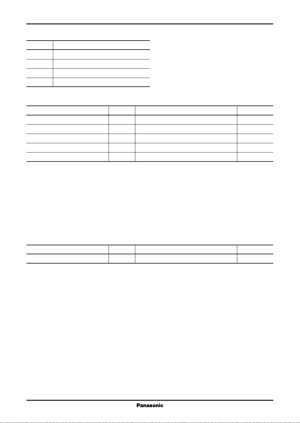
■ Pin Descriptions
Pin No. Description
1 Supply voltage pin
2N.C.
3 Output pin
4 Ground pin
■ Absolute Maximum Ratings
Parameter Symbol Rating Unit
Supply voltage V
Supply current I
2
Power dissipation
Operating ambient temperature
Storage temperature
Note) 1. The reverse insertion of this IC will cause its breakdown.
2. It will operate normally in several tens of ms after power on.
3. Use it within 100 mT of magnetic flux density, because if 100 mT or more is applied, the output of Hall IC is likely to be
inverted.
4. Since this IC requires a special assembly, its anti-moisture characteristic is poor compared with other ordinary ICs.
If high reliability is required, you should dry PCB well after mounting and mold them with resin over the PCB.
5.*1: Except for the operating ambient temperature and storage temperature, all ratings are for Ta = 25°C.
2: Shows the allowable power consumption at Ta = 100°C.
*
*
1
*
1
*
If the operation condition exceeds 62.5 mW, take measure in mounting and etc.
CC
CC
P
D
T
opr
T
stg
− 0.3 to +18 V
8mA
62.5 mW
−40 to +100 °C
−55 to +125 °C
■ Recommended Operating Range
Parameter Symbol Range Unit
Supply voltage V
2
CC
4.5 to 16 V
Page 3
Hall ICs DN6849UBS
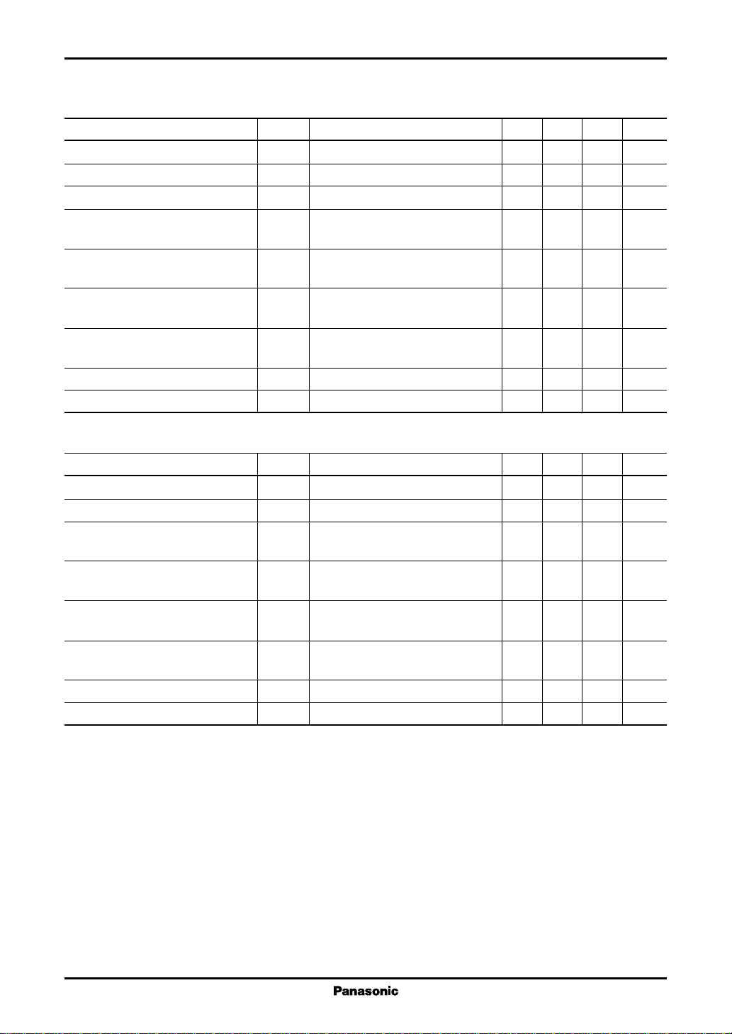
■ Electrical Characteristics
1. Electrical Characteristics at Ta = 25°C
Parameter Symbol Conditions Min Typ Max Unit
Operating magnetic flux density 1 BH-L1 VCC = 12 V −9616mT
Operating magnetic flux density 2 BL-H1 VCC = 12 V −16 −69mT
Hysteresis width BW VCC = 12 V 7 12 21 mT
Output voltage 1 V
Output voltage 2 V
Output current 1 I
Output current 2 I
Supply current 1 I
Supply current 2 I
2. Electrical Characteristics at Ta = 100°C ± 10°C
Parameter Symbol Conditions Min Typ Max Unit
Operating magnetic flux density 3 BH-L2 VCC = 12 V −15 20 mT
Operating magnetic flux density 4 BL-H2 VCC = 12 V −20 15 mT
Output voltage 3 V
Output voltage 4 V
Output current 3 I
Output current 4 I
Supply current 3 I
Supply current 4 I
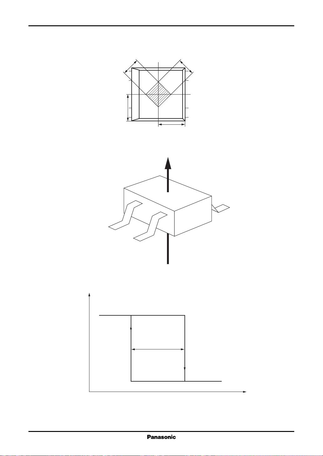
Note) 1. Symbol BH-L stands for the operating magnetic flux density where its output level varies from high to low.
2. Symbol BL-H stands for the operating magnetic flux density where its output level varies from low to high.
3. The variation of operating magnetic flux density does not depend on supply voltage due to its built-in stabilized power
source. (VCC should be confined to the range of 4.5 V to 16 V.)
VCC = 4.5 V, IO = 15 mA 0.4 V
OL1
B = 16 mT
VCC = 16 V, IO = 15 mA 0.4 V
OL2
B = 16 mT
VCC = 4.5 V, VO = 16 V 10 µA
OH1
B = −16 mT
VCC =16 V, VO = 16 V 10 µA
OH2
B = −16 mT
VCC = 4.5 V, B = 16 mT 6.5 mA
CC1
VCC = 16 V, B = 16 mT 7.0 mA
CC2
VCC = 4.5 V, IO = 15 mA 0.4 V
OL3
B = 20 mT
VCC = 16 V, IO = 15 mA 0.4 V
OL4
B = 20 mT
VCC = 4.5 V, VO = 16 V 10 µA
OH3
B = −20 mT
VCC =16 V, VO = 16 V 10 µA
OH4
B = −20 mT
VCC = 4.5 V, B = 20 mT 6.5 mA
CC3
VCC = 16 V, B = 20 mT 7.0 mA
CC4
3
Page 4
DN6849UBS Hall ICs
■ Electrical Characteristics (continued)
3. Design reference data at Ta = 25°C
Note) The characteristics listed below are not guaranteed values for design.
Parameter Symbol Conditions Min Typ Max Unit
Operating magnetic flux density ∆BH-L Difference of operating magnetic flux 0 mT
supply voltage dependency 1
Operating magnetic flux density ∆BL-H Difference of operating magnetic flux 0.6 mT
supply voltage dependency 2
Hysteresis width supply voltage ∆BW Difference of hysteresis width (BW) − 0.6 mT
1
dependency
*
Operating magnetic flux density ∆B 35mT
time lapse variation quantity
Note)*1: A test circuit shall be identical with test condition 1 in "4. Test circuit and test method".
2: At Ta = 25°C BH-L max. 16 + 5 = 21 mT
*
At Ta = 100°C BH-L max. 20 + 5 = 25 mT
Therefore, the magnetic flux density to be applied to Hall IC must be ±25 mT or more at Ta = 100°C.
Be cautious on use of a permanent magnet as it has its own temperature characteristic and time lapse variation.
1
*
1
*
density (BH-L) at VCC = 4.5 V, 16 V
density (BL-H) at VCC = 4.5 V, 16 V
at VCC = 4.5 V, 16 V
2
*
BL-H min. −16 − 5 = −21 mT
BL-H min. −20 − 5 = −25 mT
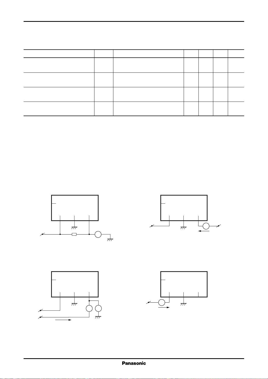
4. Test circuit and test method
Test circuit 1 Test circuit 3
BH-L, BL-H
*
2
N.C.
V
= 12 V
1
B = −16 mT to +16 mT
(at high temperature:
−20 mT to +20 mT)
3
4
1
27 kΩ
V
*
I
OH
2B = −16 mT
N.C.
4
1
V
= 16 V
CC
4.5 V
(at high temperature:
−20 mT)
3
A
V
O
I
OH
= 16 V
Test circuit 2 Test circuit 4
V
, V
*
OL1
OL2
2B = 16 mT
N.C.
4
1
VCC = 16 V
4.5 V
= 15 mA
I
O
Note) *: Measure the magnetic flux density when its output level is changed from high to low or low to high by varying the applied
magnetic flux density.
(at high temperature:
20 mT)
3
A
V
V
CC
4.5 V
I
*
CC1
N.C.
= 16 V
, I
CC2
2B = 16 mT
4
1
A
I
CC
(at high temperature:
20 mT)
3
Open
4
Page 5
Hall ICs DN6849UBS
■ Caution on use of Hall ICs
As the Hall IC is often used to detect movement, the position of a Hall IC may be changed, and there is the risk of
a change in detection level, if exposed to shock or vibration over a long period of time. Secure the IC by applying
adhesive to the package or placing in a dedicated case.
1. On mounting of the surface mount type (ESO004-P-0200 package)
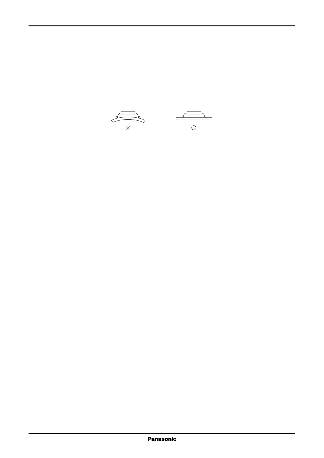
Set pin 2 to open or connect to GND. It will be damaged if it is connected to V
circuit board, the Hall IC may be highly stressed by the warp that may occur from the soldering. This may also cause
a change in the operating magnetic flux density and a deterioration of its resistance to moisture.
Be cautious to keep the device from being stressed thermally or mechanically up to the 2 mm distance from the
package.
2. On using flux in soldering
Choose a flux which does not include ingredients from halogen group, such as chlorine, fluorine, etc. The
ingredients of halogen group may enter where the lead frame and package resin joint, causing corrosion and the
disconnection of the aluminum wiring on the surface of an IC chip.
3. On fixing a Hall IC with the holder
When a Hall IC is mounted on the printed circuit board with a holder and the coefficient of expansion of the holder
is large, the lead wire of the Hall IC will be stretched and it may give a stress to the Hall IC.
If the lead wire is stressed intensely due to the distortion of holder or board, the adhesives between the package
and the lead wire may be weakened and cause a minute gap resulting in the deterioration of its resistance to moisture.
Sensitivity may also be changed by this stress.
4. Power supply line/power transmission line
If a power supply line/power transmission line becomes longer, noise and/or oscillation may be found on the line.
In this case, set the capacitor of 0.1 µF to 10 µF near a Hall IC to prevent it.
If a voltage of 18 V or more is thought to be applied to the power supply line (flyback voltage from coil or the
ignition pulse, etc.), avoid it with external components (capacitor, resistor, Zener diode, diode, surge absorbing elements, etc.).
5. V
and GND
CC
Do not reverse V
and GND. If the VCC and GND pins are reversely connected, this IC will be destroyed. If the
CC
IC GND-pin voltage is set higher than other pin voltage, the IC configuration will become same as a forward biased
diode. Therefore, it will turn on at the diode forward voltage (approximately 0.7 V), and a large current will flow
through the IC, ending up in its destruction. (This is common to Monolithic IC.)
6. Cautions on power ON of Hall IC
When a Hall IC is turned ON, the position of the magnet or looseness may change the output of a Hall IC, and a
pulse may be generated. Therefore, care should be given whenever the output state of a Hall IC is critical when the
supply power is ON.
7. When magnetic force of magnet is too strong
Output may be inverted when applying a magnetic flux density of 100 mT or more. Accordingly, magnetic flux
density should be used within the range of 100 mT.
. When mounted on the printed
CC
5
Page 6
DN6849UBS Hall ICs
■ Technical Data
• Position of a Hall element (unit in mm)
1.0
1.5
• Magneto-electro conversion characteristics
1.0
1.5
S
N
Direction of applied magnetic field
BL-H
BW
Output voltage
BH-L
Applied magnetic flux density B
6
 Loading...