

Page 1
■ Overview
The DN6848/SE/TE/S is a combination of a Hall element,
amplifier, Schmitt circuit, and stabilized power supply/temperature compensator integrated on an identical chip by using the
IC technology. It amplifies Hall element output at the amplifier, converts into a digital signal through the Schmitt circuit,
and drives the TTL or MOS IC directly.
■ Features
•
High sensitivity and low drift
•
Stable temperature characteristics due to the additional temperature compensator
•
Wide operating supply voltage range (VCC=4.5 to 16V)
•
Operating in one way magnetic field
•
TTL and MOS ICs directly drivable by output
•
Output open collector
■ Applications
•
Speed sensors
•
Position sensors
•
Rotation sensors
•
Keyboard switches
•
Microswitches
Note) This IC is not suitable for car electrical equipments.
DN6848/SE/TE/S
Hall IC (Operating Temperature Range
Topr = –
40 to +100˚C, Operating in One
Way Magnetic Field)
Unit : mm
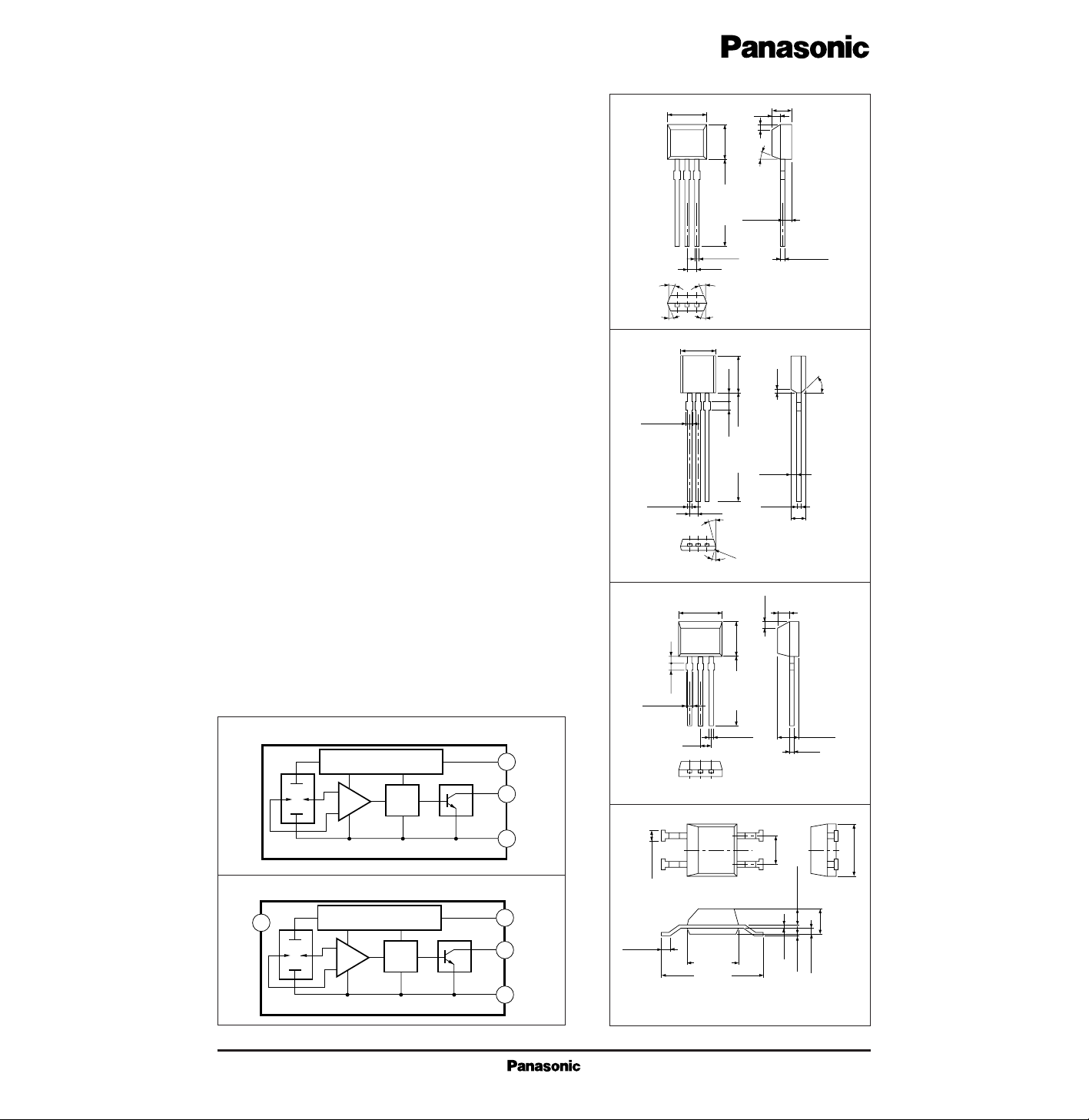
DN6848
SSIP003-P-0000A (E-3S)
1 : V
CC
2 : GND
3 : Output
0.5±0.1
5˚
123
2˚
5˚
5˚
2˚
1.27
4.0±0.3
0.7
4.5±0.3
0.43
+0.1
– 0.05
2.0±0.3
0.8±0.1
1.0
10.5±0.5
■ Block Diagram
1
Hall Element
· DN6848S
Amp. Schmitt Trigger Output Stage
3
4
2
NC
or
GND
V
CC
Output
GND
Stabilized Power Supply
Temperature Correction Circuit
DN6848SE
4.52±0.3
Unit : mm
· DN6848/SE/TE
Stabilized Power Supply
Temperature Correction Circuit
Hall Element
Amp. Schmitt Trigger Output Stage
1
3
2
V
CC
Output
GND
0.55±0.15
0.4±0.1
123
SSIP003-P-0000 (SE-3S)
DN6848TE
DN6848S
0.3 to 0.5
ESOP004-P-0200 (SOH-4D)
4.0±0.3
(1.0)(1.0)
0.6±0.15
1.27
123
SSIP003-P-0000B (TE-3S)
1
2
0.6±0.2
(1.0)(1.0)
4.52±0.3
12.5±06.5
(0.72)
1.27
2 to 5˚
2˚
R0.25
(0.6)
3.3±0.3
10.0±0.6
0.5±0.1 1.2±0.1
4
3
3.0±0.3
5.4±0.4
2˚
(0.4)
1.54±0.1
1 : V
2 : GND
3 : Output
(0.7)
1 : V
2 : GND
3 : Output
1.6
0.95±0.2
0.15
0 to 0.1
1 : V
CC
2 : NC or GND
3 : Output
4 : GND
45˚
CC
Unit : mm
(0.2)
CC
Unit : mm
3.0±0.3
1.5±0.3
0.4±0.2
Page 2
V
CC
I
CC
I
O
P
D
T
opr
T
stg
Supply voltage
Supply current
Circuit current
Power dissipation
Operating ambient temperature
Storage temperature
V
mA
mA
mW
˚C
˚C
18
8
20
150
–40 to +100
–55 to +125
Parameter Symbol Rating Unit
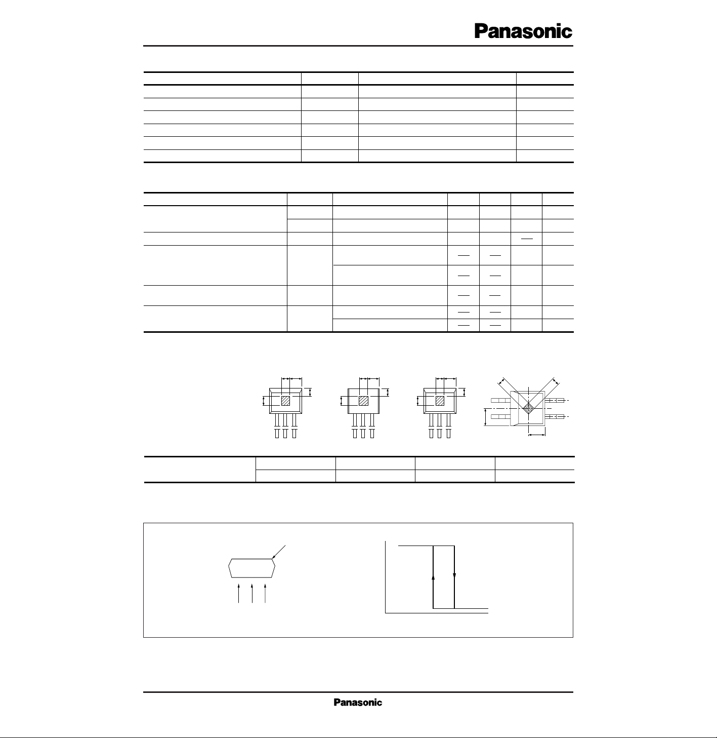
■ Absolute Maximum Ratings (Ta=25˚C)
Operating flux density
0.5B
1 (L to H)
mT9
V
CC
=12V
B
2 (H to L)
22 mT11
V
CC
=12V
Hysteresis width
1BW mT2
VCC=12V
Low output voltage V
OL
0.4 V
V
CC
=4.5 to 16V
VO=16V, B=0mT
High output current
I
OH
10 µA
Supply current
mA
V
CC
=16V
I
CC
5.5 mA
V
CC
=4.5V
6
21
0.4
1.5
V
VCC=4.5V, IO=12mA,
B=22mT
V
CC
=16V, IO=12mA,
B=22mT
Parameter Symbol Condition min typ max Unit
■ Electrical Characteristics (Ta=25˚C)
1.5
1.5
1.0
1.3
1.0 1.75
1.0
1.0
1.0
1.25
1.0 1.63
1.0
1.15
1.0 1.5
Distance from package
surface to sensor (mm)
DN6848
0.7
DN6848SE
0.42
DN6848TE
0.4
DN6848S
0.65
Unit : mm
The center of the Hall
element is in the hatched
area in the right figure.
■ Hall Element Position
Marking surface
Applied flux direction
Flux density (B)
Output voltage (V
O
)
B
1
B
2
■ Flux-Voltage Conversion Characteristics
Page 3
■ Precaution on Use
1.
Change of the operation magnetic flux density does not depend on the supply voltage, because the stabilization
power supply is built-in. (only for the range
; VCC= 4.5 to 16V)
2.
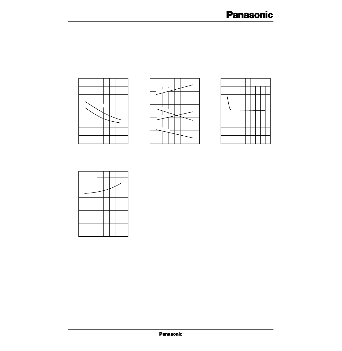
Change from “H” to “L” level increases the supply current by approx. 1mA.
V
CC
= 4.5V
Ambient temperature (˚C)
Supply current (mA)
Supply voltage – Ambient temperature
8
7
6
5
4
3
2
1
0
–50 –25 0 25 50 75 100
V
CC
= 16V
Ambient temperature (˚C)
Operating flux density (mT)
Operating flux density – Ambient temperature
25.0
22.5
20.0
17.5
15.0
12.5
10.0
7.5
5.0
2.5
–50 –25 0 25 50
V
CC
= 4.5 to 16V
B
H→L
75 100
Sam
ple 1
Sample 2
Sample 3
Sample 4
Ambient temperature (˚C)
Output “L” level voltage (mV)
Output low level voltage – Ambient temperature
100
90
80
70
60
50
40
30
20
10
0
–50 –25 0 25 50
V
CC
=12V
I
O
=12mA
75 100 125
Supply voltage (V)
Operating flux density (mT)
Operating flux density – Supply voltage
20.0
17.5
15.0
12.5
10.0
7.5
5.0
2.5
0
02468101214161820
Ta =25˚C
■ Characteristics Curve
 Loading...