

Page 1

0RGHO1R '0;7
&217(176
SERVICE MANUAL
3UHFDXWLRQV
%ORFN'LDJUDP
7URXEOHVKRRWLQJ
6FKHPDWLF'LDJUDPV
([SORGHG9LHZV
.H\3DUWV
3URGXFW6SHFLILFDWLRQV
Page 2
1.PRECAUTIONS
Prior to shipment from the factory,the products are strictly inspected to conform with recognized product safety and
Electrical codes of the countries in which they are to be sold.However, in order to maintain such compliance,it is
equally important to implement the following precautions when a set is being serviced.
1-1.Safety Precautions
1) Before returning an instrument to the customer, always
make a safety check of the entire instrument, including, but
not limited to, the following items:
(1) Be sure that no built-in protective devices are defective
or have been defeated during servicing.
(1) Protective shields are provided to protect both the
technician and the customer. Correctly replace all
missing protective shields, including any remove for
servicing convenience.
(2) When reinstalling the chassis and/or other
assembly in the cabinet, be sure to put back in place
all protective devices, including, but not limited to,
nonmetallic control knobs, insulating fish papers,
adjustment and compartment covers/shields, and
isolation resistor/capacitor networks. Do not operate
this instrument or permit it to be operated without all
protective devices correctly installed and functioning.
(2) Be sure that there are no cabinet opening through which
adults or children might be able to insert their fingers
and contact a hazardous voltage. Such openings
include, but are not limited to, excessively wide
cabinet ventilation slots, and an improperly fitted
and/or incorrectly secured cabinet back cover.
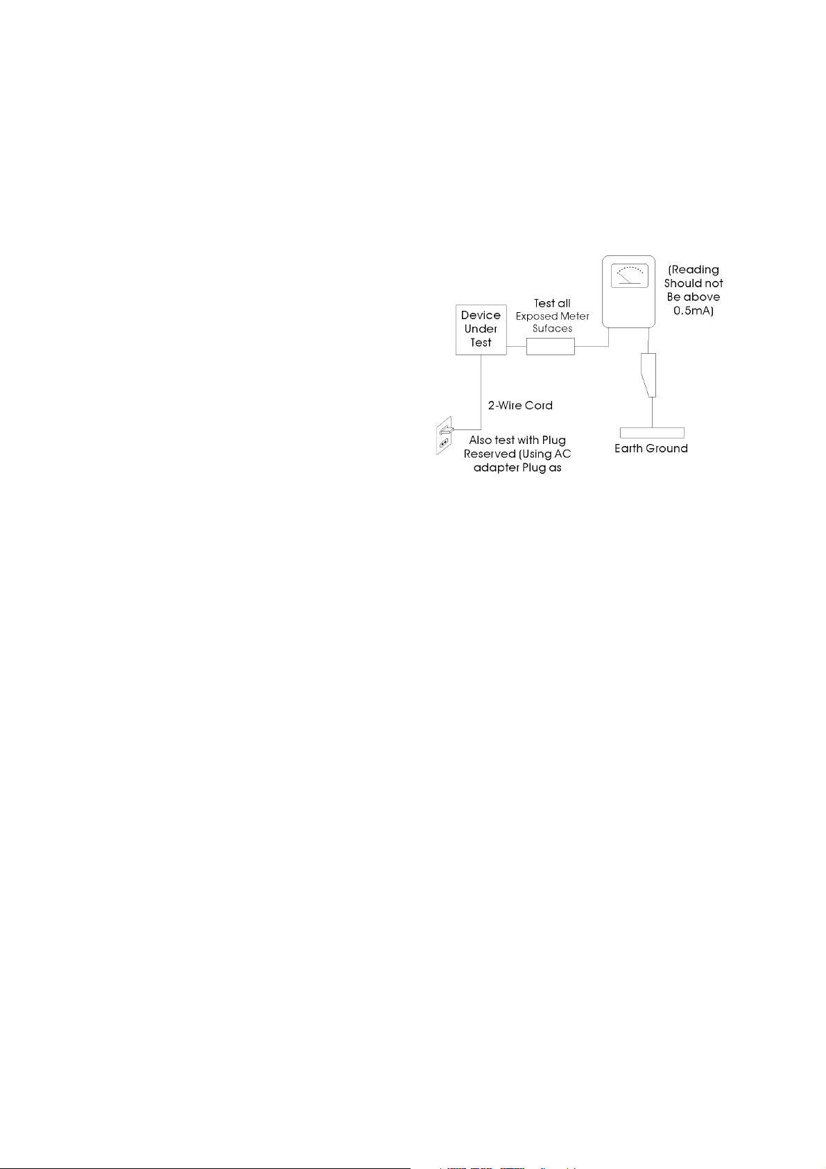
(3) Leakage Current Hot Check-With the instrument
completely reassembled, plug the AC line cord
directly into a 120V AC outlet. (Do not use an
isolation transformer during this test.) Use a leakage
current tester or a metering system that complies with
American National Standards institute (ANSI) C101.1
Leakage.
Current for Appliances and underwriters Laboratories
(UL) 1270 (40.7). With the instrument’s AC switch
first in the ON position and then in the OFF position,
measure from a known earth ground (metal water pipe,
conduit, etc.) to all exposed metal parts of the
instrument (antennas, handle brackets, metal cabinets,
screwheads, metallic overlays, control shafts, etc.),
especially and exposed metal parts that offer an
electrical return path to the chassis.
Any current measured must not exceed 0.5mA.
Reverse the instrument power cord plug in the outlet
and repeat the test.
AC Leakage Test
Any measurements not within the limits specified
herein indicate a potential shock hazard that must be
eliminated before returning the instrument to the
customer.
(4) Insulation Resistance Test Cold Check-(1) Unplug the
power supply cord and connect a jumper wore
between the two prongs of the plug. (2) Turn on the
power switch of the instrument. (3) Measure the
resistance with an ohmmeter between the jumpered
AC plug and all exposed metallic cabinet parts on the
instrument, such as screwheads, antenna, control
shafts, handle brackets, etc. When an exposed
metallic part has a return path to the chassis, the
reading should be between 1 and 5.2 megohm. When
there is no return path to the chassis, the reading must
be infinite. If the reading is not within the limits
specified, there is the possibility of a shock hazard,
and the instrument must be re-pared and rechecked
before it is returned to the customer.
Page 3
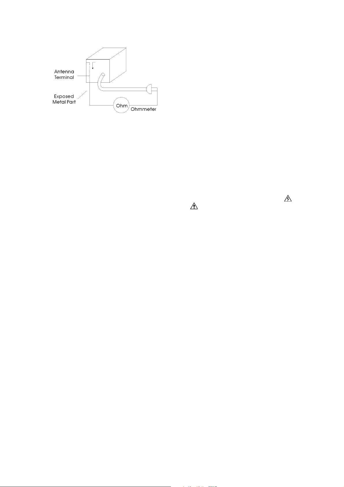
Insulation Resistance Test
2) Read and comply with all caution and safety related
notes non or inside the cabinet, or on the chassis.
voltage, and (5) antenna wiring. Always inspect in all
areas for pinched, out-of-place, or frayed wiring. Do
not change spacing between a component and the
printed-circuit board, Check the AC power cord for
damage.
5) Components, parts, and/or wiring that appear to have
overheated or that are otherwise damaged should be
replaced with components, parts and/or wiring that
meet original specifications. Additionally determine
the cause of overheating and/or damage and, if
necessary, take corrective action to remove and
potential safety hazard.
3) Design Alteration Warning-Do not alter of add to the
mechanical or electrical design of this instrument.
Design alterations and additions, including but not
limited to, circuit modifications and the addition of
items such as auxiliary audio output connections,
might alter the safety characteristics of this instrument
and create a hazard to the user. Any design alterations
or additions will make you, the service, responsible
for personal injury or property damage resulting there
from.
4) Observe original lead dress. Take extra care to assure
correct lead dress in the following areas:
(1) near sharp edges, (2) near thermally hot parts (be
sure that leads and components do not touch
thermally hot parts), (3) the AC supply, (4) high
1-2 Servicing Precautions
CAUTION: Before servicing Instruments covered by this
service manual and its supplements, read and follow the
Safety Precautions section of this manual.
Note: If unforeseen circument create conflict between the
following servicing precautions and any of the safety
precautions, always follow the safety precautions.
Remember; Safety First
1-2-1 General Serving Precautions
(1) a. Always unplug the instrument’s AC power cord from
the AC power source before (1) removing or
reinstalling any component, circuit board, module or
any other instrument assembly. (2) disconnecting
any instrument electrical plug or other electrical
connection. (3) connecting a test substitute in
parallel with an electrolytic capacitor in the
instrument.
6) Product Safety Notice-Some electrical and mechanical
parts have special safety-related characteristics which
are often not evident from visual inspection, nor can
the protection they give necessarily be obtained by
replacing them with components rated for higher
voltage, wattage, etc. Parts that have special safety
characteristics are identified by shading, an (
(
) on schematics and parts lists. Use of a substitute
replacement that does not have the same safety
characteristics as the recommended replacement part
might created shock, fire and/or other hazards.
Product safety is under review continuously and new
instructions are issued whenever appropriate.
b. Do not defeat any plug/socket B+ voltage interlocks
with which instruments covered by this service
manual might be equipped.
c. Do not apply AC power to this instrument and/or any
of its electrical assemblies unless all solid-state
device heat sinks are correctly installed.
d. Always connect a test instrument’s ground lead to
the instrument chassis ground before connecting the
test instrument positive lead. Always remove the test
instrument ground lead last.
Note: Refer to the Safety Precautions section ground
lead last.
(2) The service precautions are indicated or printed on the
cabinet, chassis or components. When servicing,
follow the printed or indicated service precautions
and service materials.
(3) The components used in the unit have a specified flame
resistance and dielectric strength.
When replacing components, use components which
) or a
Page 4

have the same ratings, by ( ) or by ( ) in the
circuit diagram are important for safety or for the
characteristics of the unit. Always replace them with
the exact replacement components.
(4) An insulation tube or tape is sometimes used and some
components are raised above the printed wiring board
for safety. The internal wiring is sometimes clamped
to prevent contact with heating components. Install
such elements as they were.
(5) After servicing, always check that the removed screws,
components, and wiring have been installed correctly
and that the portion around the serviced part has not
been damaged and so on. Further, check the insulation
between the blades of the attachment plus and
1-3 ESD Precautions
Electrostatically Sensitive Devices (ESD)
Some semiconductor (solid static electricity) devices can
be damaged easily by static electricity.
Such compo9nents commonly are called Electrostatically
Sensitive Devices (ESD). Examples of typical ESD devices
are integrated circuits and some field-effect transistors and
semiconductor chip components. The following techniques
of component damage caused by static electricity.
(1) immediately before handling any semiconductor
components or semiconductor-equipped assembly,
drain off any electrostatic charge on your body by
touching a known earth ground. Alternatively, obtain
and wear a commercially available discharging wrist
strap device, which should be removed for potential
shock reasons prior to applying power to the unit
under test.
(2) after removing an electrical assembly equipped with
ESD devices, place the assembly on a conductive
surface such as aluminum foil, to prevent electrostatic
charge buildup or exposure of the assembly.
accessible conductive parts.
1-2-2 Insulation Checking Procedure
Disconnect the attachment plug from the AC outlet and
turn the power ON. Connect the insulation resistance meter
(500V) to the blades of the attachment plug. The insulation
resistance between each blade of the attachment plug and
accessible conductive parts (see note) should be more than
1 Megohm.
Note: Accessible conductive parts include metal panels,
input terminals, earphone jacks, etc.
devices.
(6) Do not remove a replacement ESD device from its
protective package until immediately before you are
ready to install it. (Most replacement ES devices are
packaged with leads electrically shorted together by
conductive foam, aluminum foil or comparable
conductive materials).
(7) Immediately before removing the protective materials
from the leads of a replacement ES device touch the
protective material to the chassis or circuit assembly
into which the device will be installed.
CAUTION: Be sure no power is applied to the chassis or
circuit, and observe all other safety precautions.
(8) Minimize bodily motions when handling unpackaged
replacement ESD devices. (Otherwise harmless
motion such as the brushing together of your clothes
fabric or the lifting of your foot from a carpeted floor
can generate static electricity sufficient to damage an
ESD device).
(3) Use only a grounded-tip soldering iron to solder or
unsolder ESD device.
(4) Use only an anti-static solder removal devices. Some
solder removal devices not classified as “anti-static”
can generate electrical charges sufficient to damage
ESD devices.
(5) Do not use freon-propelled chemicals. These can
generate electrical charges sufficient to damage ESD
Page 5
1-4. Handling the LCD Module
In case the screen is damaged and the internal liquid
leaks,do not suck or drink the internal fuid. Nor do you
touch it either ,otherwise you might be poisoned or get a
rash with your skin,If the internal fluid enters your
mouth,rinse with water.If itadheres to your skin or
clothes,wipe it away with alcohol and then wash with water.
If it enters your eyes,wash with running water immediately.
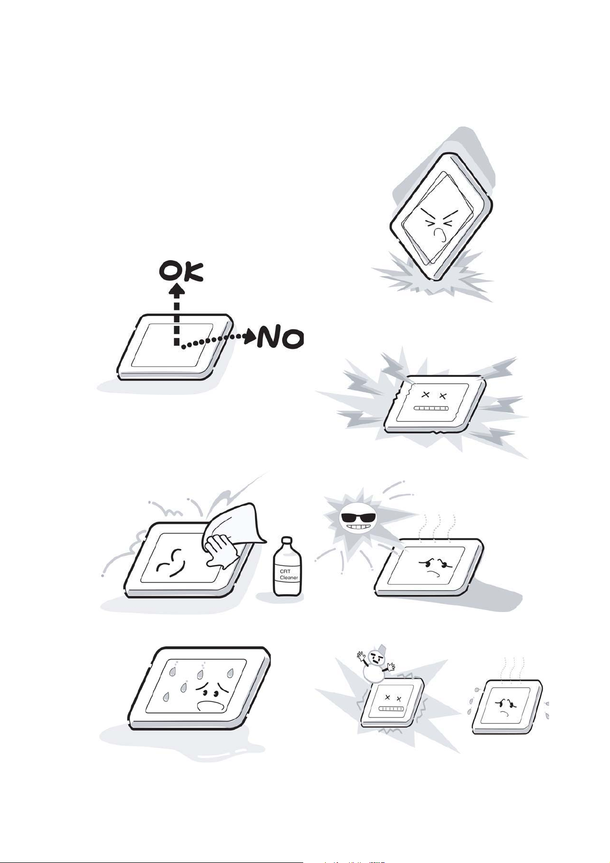
Precautions for handling the LCD module
The LCD module can be easily damaged during assembly
or disassembly.Observe the following precautions when
handling the LCD module:
1. When installing the LCD module in the LCD cover,be
sure to seat it so that it is properly aligned and
maximum visibility of the display is maintained.
4. Glass is used in the panel ,so be careful not to drop it
or let it strike a hard object ,which could cause
breakage or cracks.
5. CMOS-LSI circuits are used in the module,so guard
against damage from electrostatic discharge.Be sure to
wear aa wrist or ankle ground when handling the
module.
2. If the panel’s surface gets dirty,wipe it with cotton or a
soft cloth.If it is still dirty,try breathing on the surface
to create a light condensate and wipe it again.If the
surface is very dirty,we recommend a CRT cleaning
agent.Apply the agent to a cloth and then wipe the
panel’s surface .Do not apply cleanser directly to the
panel .Also,neverscratch the suface.
3. If water or other liquid is left on the panel’s surface for
a long period,it can change the screen’s tint or stain it.
Be sure to quickly wipe off any liquid.
6. Do not expose the module to direct sunlight or strong
ultraviolet rays for long periods.
7. Do not store the module a temperatures below
specifications.Cold can cause the liquid crystals to
freeze,lose their elasticity or otherwise suffer damage.
Page 6
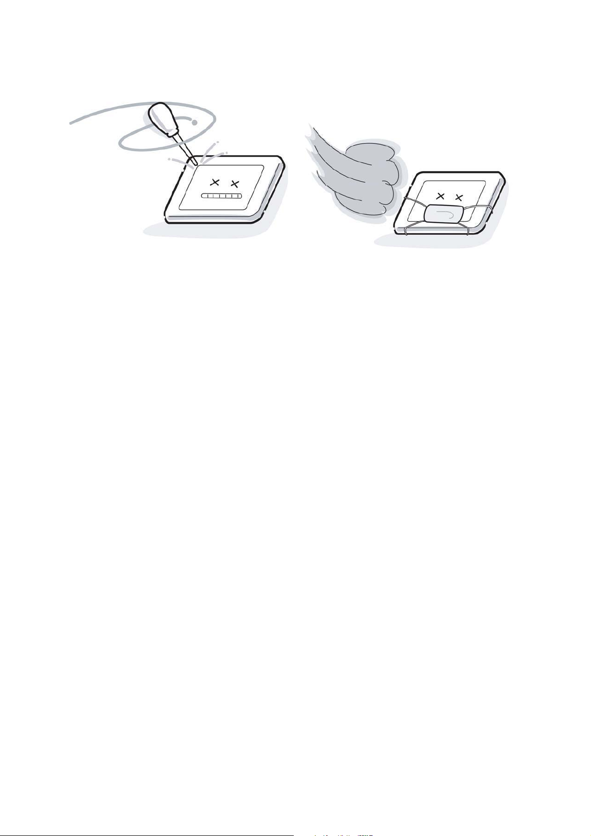
8. Do not disassemble the LCD module.Disassembly can
cause malfunctions.
9. If you transport the module,do not use packing
material that contains epoxy resin(amine)or silicom
glue(alcohol or oxime).These materials can release gas
that can damage the panel’s polarization.
Page 7
TR901E-1(EURO+DVB-T+DVD) SPECIFICATION
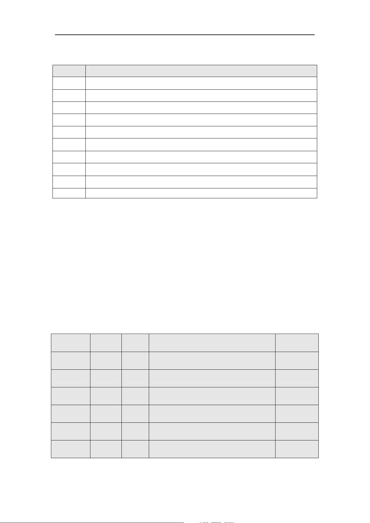
CONTENT
PAGE ITEM
1 CONTENT
1 REVISION HISTORY
2 GENERAL DISCRIPTION
2 FEATURES
3 FUNCTION LAYOUT
5 PCB DIMENSIONS
5 IR CONTROL SCHEMATICS
6 KEY BOARD SCHEMATICS
6 INTERFACE DEFINITION
10 CONFIGURATION & GENERAL PRECAUTIONS
REVISION HISTORY
VERSION DATE PAGE DISCRIPTION AUTHOR
1.0 08.09.10 All First issued Liu Lili
1.1 08.11.13 P8 Correct the description of CN28 JinhuaHuang
- 1 -
Page 8
TR901E-1(EURO+DVB-T+DVD) SPECIFICATION
1. GENERAL DESCRIPTION
TR901E-1 is a multi-purpose LCD&PDP control board. It is suitable for UK market. It supports
26~47 inch LCD panel with dual/single LVDS interface and its resolution is up to 1920x1080.
TR901E-1 supports DVB-TˈTeletext, Nicam, PIP, dual HDMI, dual SCART , YPbPr/YCbCr, PC and
other functions.
TR901E-1 provides expansible functions such as DVD and Card reader.
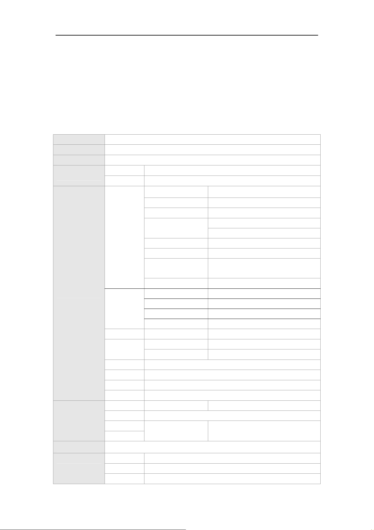
2. FEATURES
CHIPSET AX68+ZRA39162
MARKET AREA
OSD LANGUAGE English, French, Spanish, Italian, Portuguese, German.(Option)
PANEL
VIDEO INPUT
AUDIO INPUT
Europe, UK
Interface Dual/Single LVDS interface
Resolution Up to 1920x1080(It does not support 10Bit Panel.)
Tuner receiving range 49MHz – 863MHz
Input impedance 75ƻ
Video System PAL, SECAM
Sound System
ATV
DTV
PC-RGB Format Up to 1280x1024@60Hz
CVBS
S-VIDEO S-Y:0.7Vp-p+/-5% S-C:0.3Vp-p+/-5%
YPbPr/YCbCr 480i, 480p, 576i, 576p, 720p, 1080i, 1080p
HDMI 480i, 480p, 576i, 576p, 720p, 1080i, 1080p
SCART SCART1: RGB/CVBS; SCART2: CVBS/YC
PC-RGB Earphone input 0.2 – 2.0 Vrms
YUV Left and Right audio input terminal
CVBS
S-VIDEO
Max.Storage Channels 199CH
Colour Killer level
Teletext Error
Sensitivity
NICAM sensitivity
Modulation COFDM2k/8k,QPSK,16QAM,64QAM
Video System MPEG-2 MP@ML
Audio System MPEG-1/2 Layer 1,2,3
Basic Functions EPG,Subtitle,Teletext(EURO),MHEG-5(UK)
Video System PAL,SECAM
Video level 1.0 Vp-p +/-5%
L/R RCA input 0.2 – 2.0 Vrms
BG, DK, I, L/L’
NICAM/A2
30dBuV
50dBuV
45dBuV
AUDIO OUTPUT 2X9W(8ohm 24V power supply)
Requirement 24V, 12V, 5V
POWER
To Panel 5V, 12V( Also can support 18V by select suitable power supply.)
Management Low power consumption mode; standby< 1W
- 2 -
Page 9
TR901E-1(EURO+DVB-T+DVD) SPECIFICATION
COMB FILTER 3D
DEINTERLACE 3D
WEAK SIGNAL
ENHANCEMENT
NOICE
REDUCTION
NICAM/A2 YES
TELETEXT 3000Pages
PIP YES
KEY FUNCTION INPUT/EXIT, MENU, VOL+/-, CH+/-, STANDBY.(Control by remote control)
MODULES
TERMINALS INPUT
YES
YES
CARD READER,USB EXPANSIBLE
Build In DVD
TV INPUT 1 IEC 75ƻ
PC-RGB 1 D-SUB 15Pin terminal(blue)
S-VIDEO 1 S-Video terminal(black)
CVBS 1 RCA terminal(yellow)
YPbPr Input 3 RCA terminals( Green, Blue, Red)
HDMI 2 HDMI terminal
SCART 2 SCART terminal
CVBS AUDIO 2 RCA terminals(white, red)
YPbPr Audio Input 2 RCA terminals(white, red)
PC-RGB AUDIO 1 Earphone terminal(black)
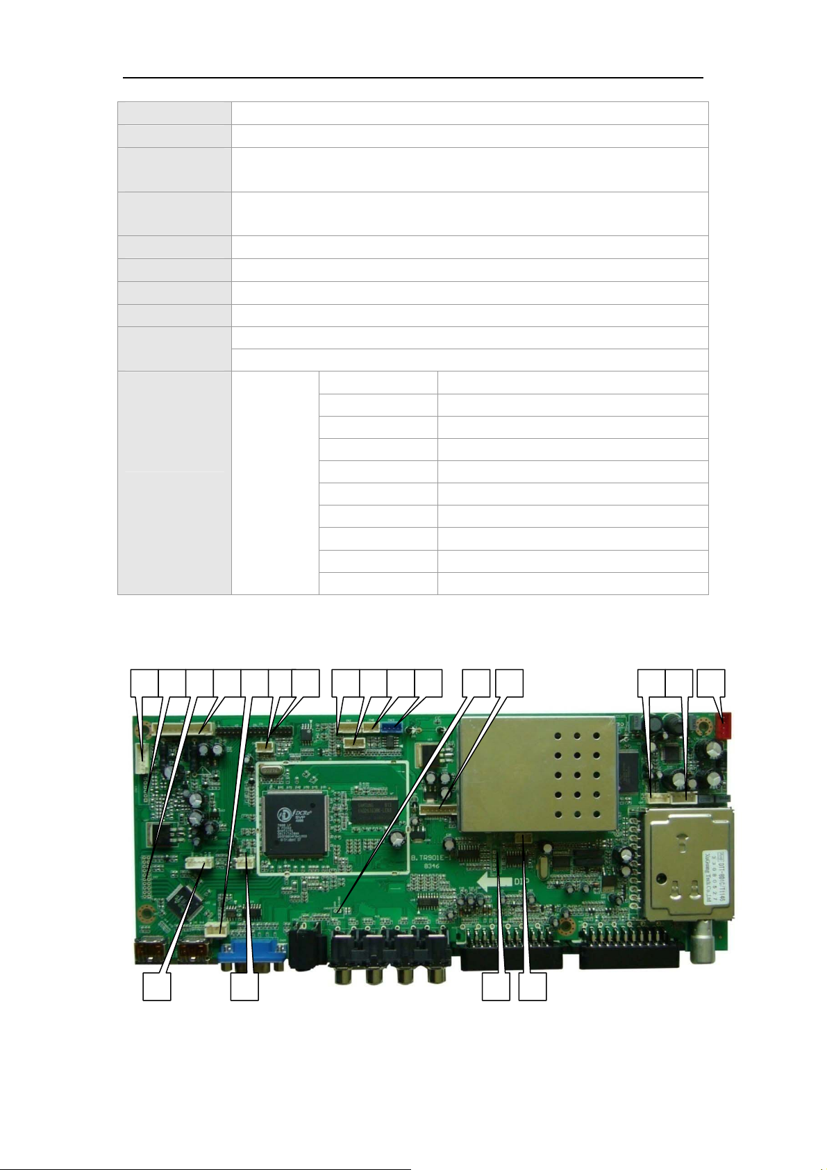
3. FUNCTION LAYOUT
TOP VIEW OF LCD CONTROL BOARD
1 2 3 4 5 6 7 8 9 10 11 12 14 15
17 18
19 36
1613
- 3 -
Page 10
TR901E-1(EURO+DVB-T+DVD) SPECIFICATION
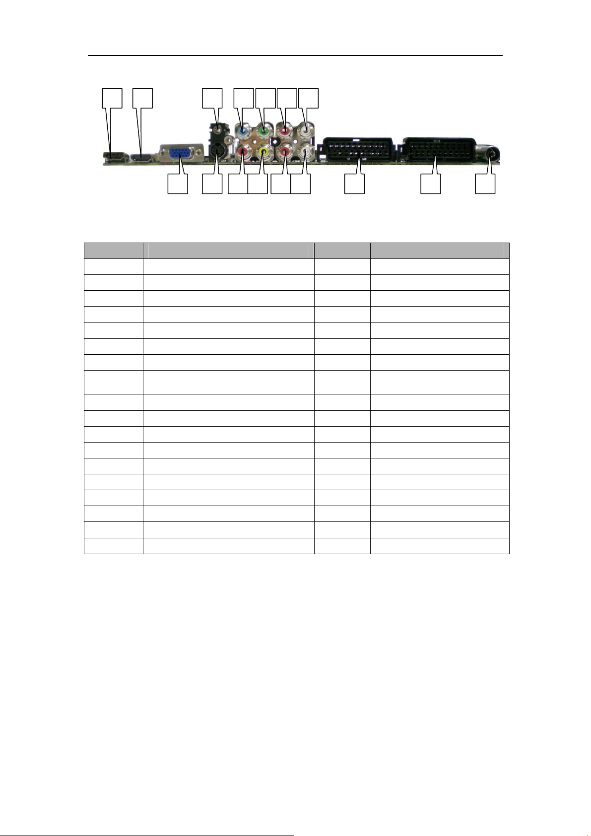
20 21 22 23 24 25 26
27 28 29 30 31 32 33 34 35
INTERFACE FUNCTION DESCRIPTION
NO. DESCRIPTION NO. DESCRIPTION
1(CN29) Inverter Connector 19(CN17)
2(CN14) DVD Power Supply Connector 20 HDMI1 In
3(CN3) External HDMI Connector 21 HDMI2 In
4(CN28) Main Power Supply In Connector 22 PC-Audio In
5(CN4) Debugging Interface 1 23 YPbPr-Pb In
6(CN5) Key Board Connector 24 YPbPr-Y In
7(CN1) LVDS Panel Connector 25 YPbPr-Right Audio In
DVD IR and Audio Input Connector
8(CN2) IR Receiver and LED Indicator Connector 26 YPbPr-Left Audio In
9(CN6) Debugging Interface 2 27 PC-RGB In
10(CN8) Extended GPIO 28 S-Video In
11(CN13) Debugging Interface 3 29 YPbPr-Pr In
12(CN10) CVBS Video Input For DVD Connector 30 CVBS In
13(CN16) Extended YPbPr (without DVB) 31 CVBS &S-Video Right Audio In
14(CN7) Debugging Interface4 32 CVBS &S-Video Left Audio In
15(CN18) Speaker Connector 33 SCART1
16(CN19) Power Supply for Amplifier Connector 34 SCART2
17(CN11) PDP Panel Connector 35 TV signal In
18(CN12) Extended GPIO 36 DVB Audio In
- 4 -
Page 11
TR901E-1(EURO+DVB-T+DVD) SPECIFICATION
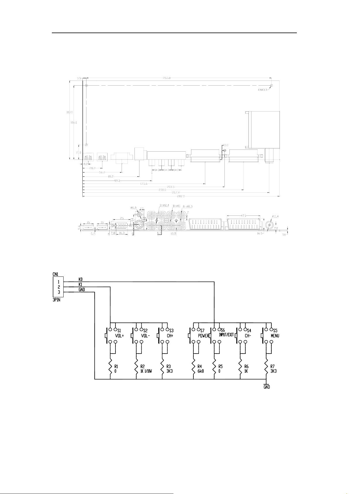
4. PCB DIMENSION
The height of the whole control board is: 32mm
5. KEY BOARD SCHEMATICS
- 5 -
Page 12
TR901E-1(EURO+DVB-T+DVD) SPECIFICATION
n
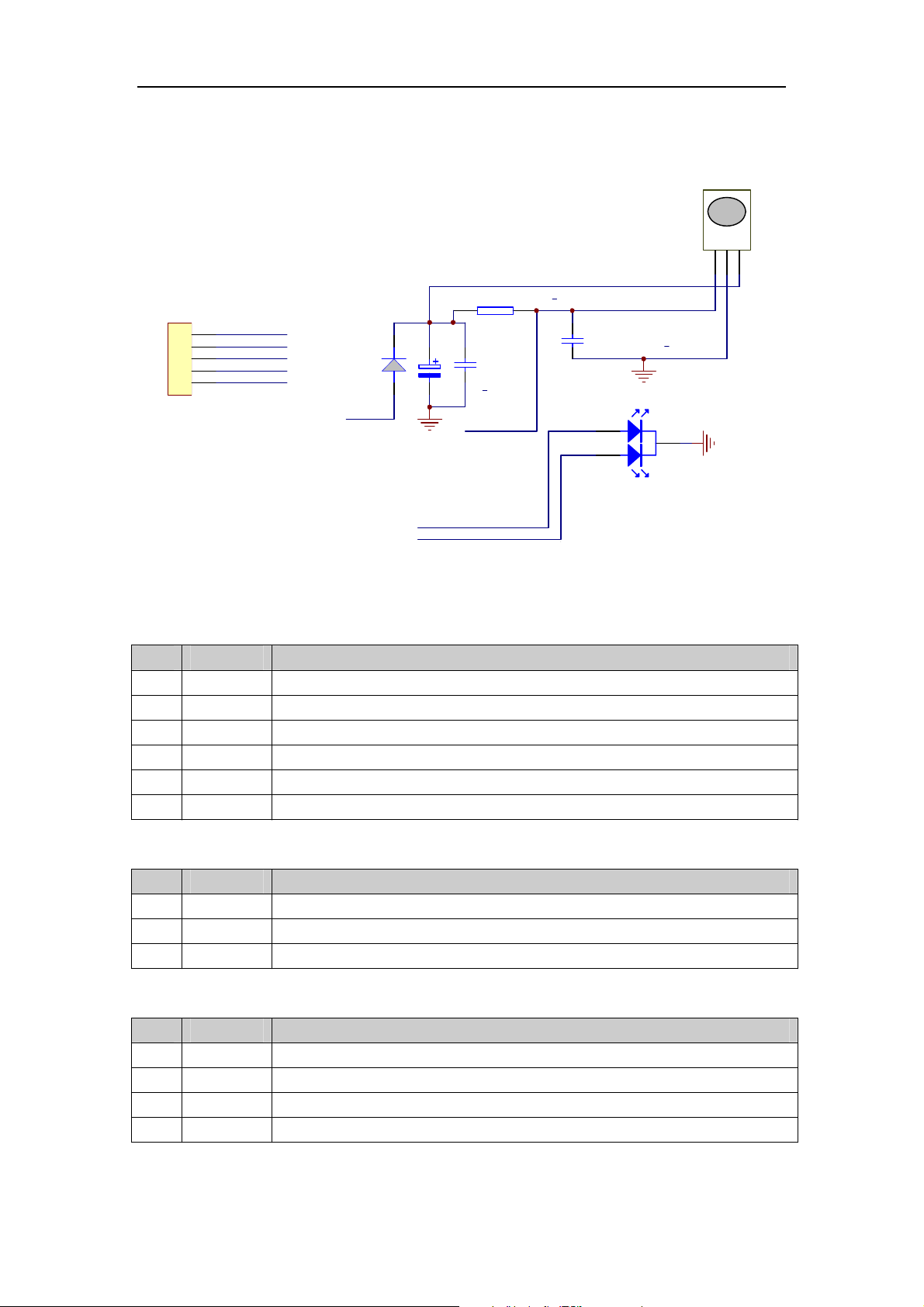
6. IR BOARD SCHEMATICS
&1
3,1
*1'
,5
*51B(1
5('B(1
9
,1
9
'
(
X)9
.RKP:
5
&
X)<99
°
&
,5
Red green diameter m and commo
cathode figure of fog general luminance
5('B(1
*51B(1
&
S)1329
'
5.0m
5(
9
7. INTERFACE DEFINITION
ƹ CN29(6PIN/2.0): INVERTER CONNECTOR
NO. SYMBOL DESCRIPTION
1 +12V +12V DC Power Supply
2 +12V +12V DC Power Supply
3 BL_ON Back-light ON/OFF control
4 ADJ Brightness Adjustment
5 GND Ground
6 GND Ground
ƹ CN5(3PIN/2.0): KEY BOARD CONNECTOR
NO. SYMBOL DESCRIPTION
1 GND Ground
2 K1 Key1
3 K0 Key0
ƹ CN18(4PIN/2.54): SPEAKER CONNECTOR
NO. SYMBOL DESCRIPTION
1 LOUT Left Audio Channel Out
2 GND Ground
3 GND Ground
4 ROUT Right Audio Channel Out
- 6 -
Page 13
TR901E-1(EURO+DVB-T+DVD) SPECIFICATION
ƹ CN14(6PIN/2.0): DVD POWER SUPPLY CONNECTOR
NO. SYMBOL DESCRIPTION
1 DVD5V +5V DC Power Supply
2 DVD5V +5V DC Power Supply
3 GND Ground
4 GND Ground
5 DVD12V +12V DC Power Supply
6 DVD12V +12V DC Power Supply
ƹ CN4(3PIN/2.54): DEBUGGING INTERFACE 1
NO. SYMBOL DESCRIPTION
1 SCL Clock
2 SDA Data
3 GND Ground
ƹ CN10(2IN/2.0): CVBS VIDEO INPUT FOR DVD CONNECTOR
NO. SYMBOL DESCRIPTION
1 D-DVBS DVD-CVBS Input
2 GND Ground
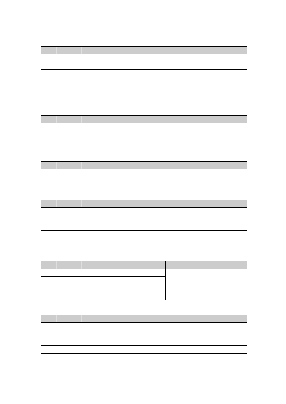
ƹ CN2(5PIN/2.0): IR RECEIVER AND LED INDICATOR CONNECTOR
NO. SYMBOL DESCRIPTION
1 5V +5V DC Power Supply
2 LED-R Red Indicator
3 LED-G Green Indicator
4 IR Remote Receiver
5 GND Ground
ƹ CN19(4PIN/2.54): POWER SUPPLY FOR AMPLIFIER CONNECTOR
NO. SYMBOL DESCRIPTION ELECTRIC CURRENT
1 24V +24V DC Power Supply
2 24V +24V DC Power Supply
3 GND Ground
4 GND Ground
800mA
ƹ CN17(5PIN/2.0): DVD IR AND AUDIO INPUT CONNECTOR
NO. SYMBOL DESCRIPTION
1 DVD-R DVD Right-Channel Audio Input
2 GND Ground
3 DVD-L DVD Left-Channel Audio Input
4 GND Ground
5 DVD-IR DVD IR Receiver
- 7 -
Page 14
TR901E-1(EURO+DVB-T+DVD) SPECIFICATION
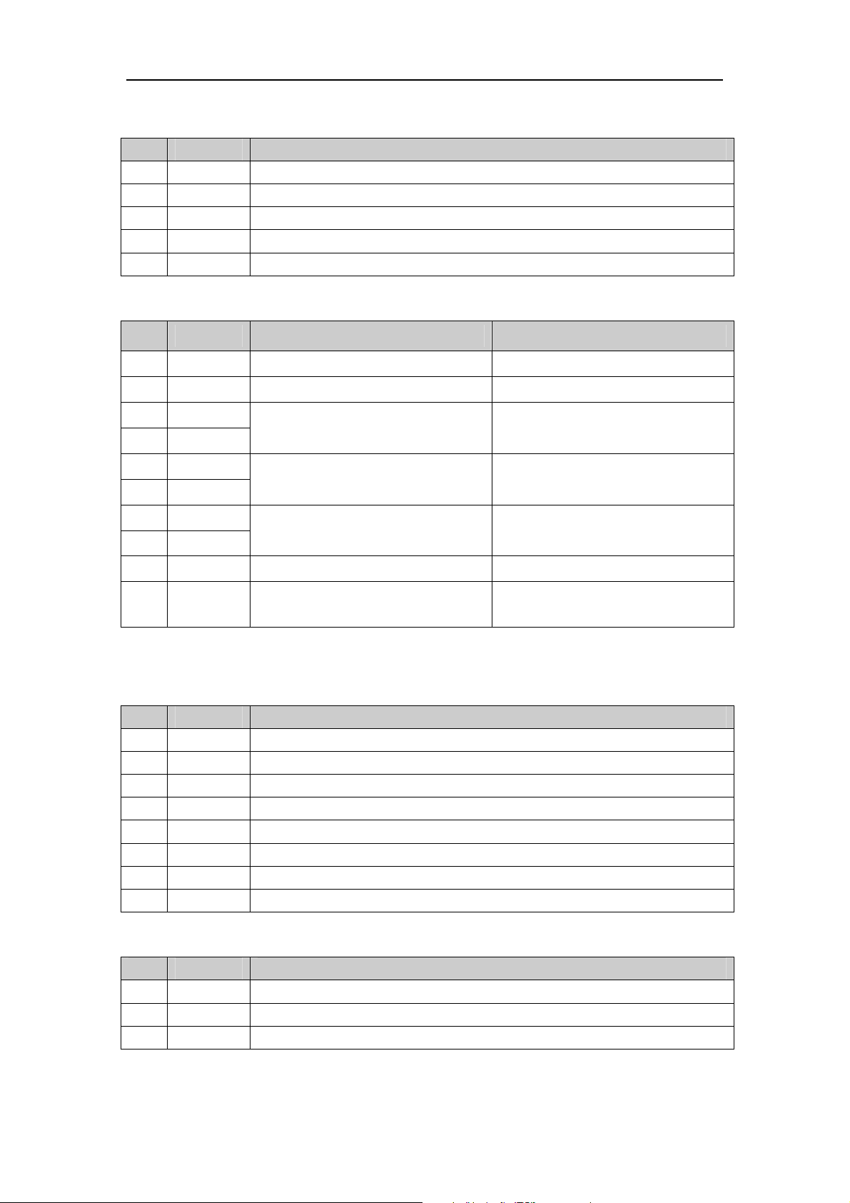
ƹ CN11(5PIN/2.0): PDP PANEL CONNECTOR
NO. SYMBOL DESCRIPTION
1 DIS PDP Display Enable
2 RLY Relay On for LG PDP
3 LG VS-ON Control for LG-PDP
4 S VS-ON Control for Samsung-PDP
5 GND Ground
ƹ CN28(10PIN/2.54): MAIN POWER SUPPLY CONNECTOR
NO. SYMBOL DESCRIPTION ELECTRIC CURRENT
1 5VSB Power Supply Standby 80mA
2 PWD Power Supply Switch Control ---
3 GND
4 GND
5 P5V
+5V Panel Power Supply
6 P5V
7 5V
8 5V
9 GND Ground
10 12V +12V DC Power Supply
Ground ---
Panel Electric Current
˄Refer to the Connected Panel˅
+5V Power Supply
+electric Current of extended module
100mA+Panel Electric Current
+electric Current of extended module
ƹ CN16(8PIN/2.0): DVB VIDEO INPUT CONNECTOR
NO. SYMBOL DESCRIPTION
1 BLU Blue/YPbPr-Pb
2 GND Ground
3 RED Red/YPbPr-Pr
4 GND Ground
5 GRN Green/YPbPr-Y
6 GND Ground
7 CVBS CVBS Input
8 GND Ground
1200mA
---
ƹ CN12(3PIN/2.0): GPIO
NO. SYMBOL DESCRIPTION
1 SW1 Switch 1
2 SW2 Switch 2
3 GND Ground
ƹ CN1(2x18PIN/2.0): LVDS PANEL CONNECTOR
- 8 -
Page 15
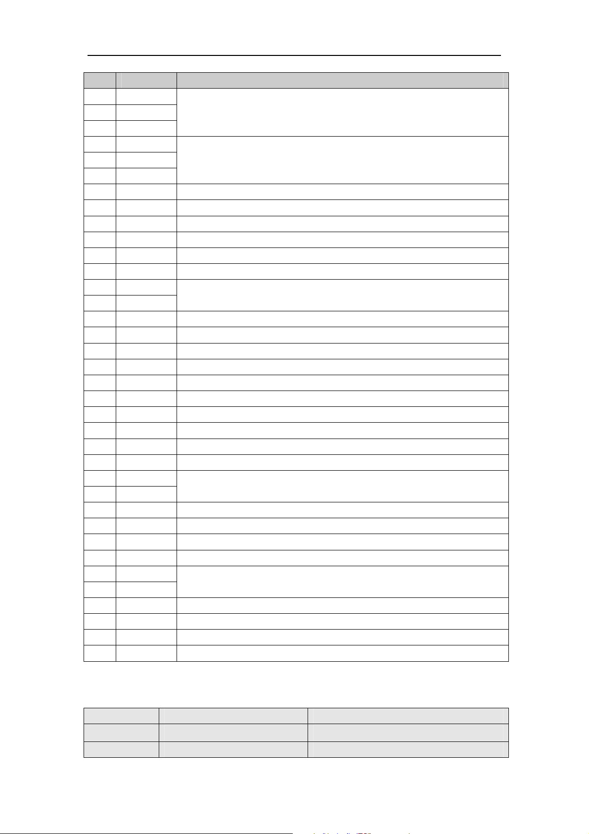
TR901E-1(EURO+DVB-T+DVD) SPECIFICATION
NO. SYMBOL DESCRIPTION
1 VSEL
2 VSEL
3 VSEL
4 GND
5 GND
6 GND
7 RXO0- LVDS ODD 0- Signal
8 RXO0+ LVDS ODD 0+ Signal
9 RXO1- LVDS ODD 1- Signal
10 RXO1+ LVDS ODD 1+ Signal
11 RXO2- LVDS ODD 2- Signal
12 RXO2+ LVDS ODD 2+ Signal
13 GND
14 GND
15 RXOC- LVDS ODD Clock- Signal
16 RXOC+ LVDS ODD Clock+ Signal
17 RXO3- LVDS ODD 3- Signal
18 RXO3+ LVDS ODD 3+ Signal
19 RXE0- LVDS EVEN 0- Signal
20 RXE0+ LVDS EVEN 0+ Signal
21 RXE1- LVDS EVEN 1- Signal
22 RXE1+ LVDS EVEN 1+ Signal
23 RXE2- LVDS EVEN 2- Signal
24 RXE2+ LVDS EVEN 2+ Signal
25 GND
26 GND
27 RXEC- LVDS EVEN Clock- Signal
28 RXEC+ LVDS EVEN Clock+ Signal
29 RXE3- LVDS EVEN 3- Signal
30 RXE3+ LVDS EVEN 3+ Signal
31 GND
32 GND
33 CON1 CON1
34 DISPLAY Display
35 POWER/SCL Power/IIC Clock
36 POWER/SDA Power/IIC Data
Note1: This specification aims at LCD ÿ s interface definition. TR901E-1 also supports PDP panel,
Normally, pin 31~36 are not used for LCD panel application. For detailed information please refer to
the table.
Thirty-fifth pin of CN1 Thirty-sixth pin of CN1
LCD Panel Power Power
PDP Panel SCL SDA
Power for Panel
Ground
Ground
Ground
Ground
- 9 -
Page 16
Page 17
Page 18
Page 19
Page 20
Page 21
Page 22
Page 23
Page 24
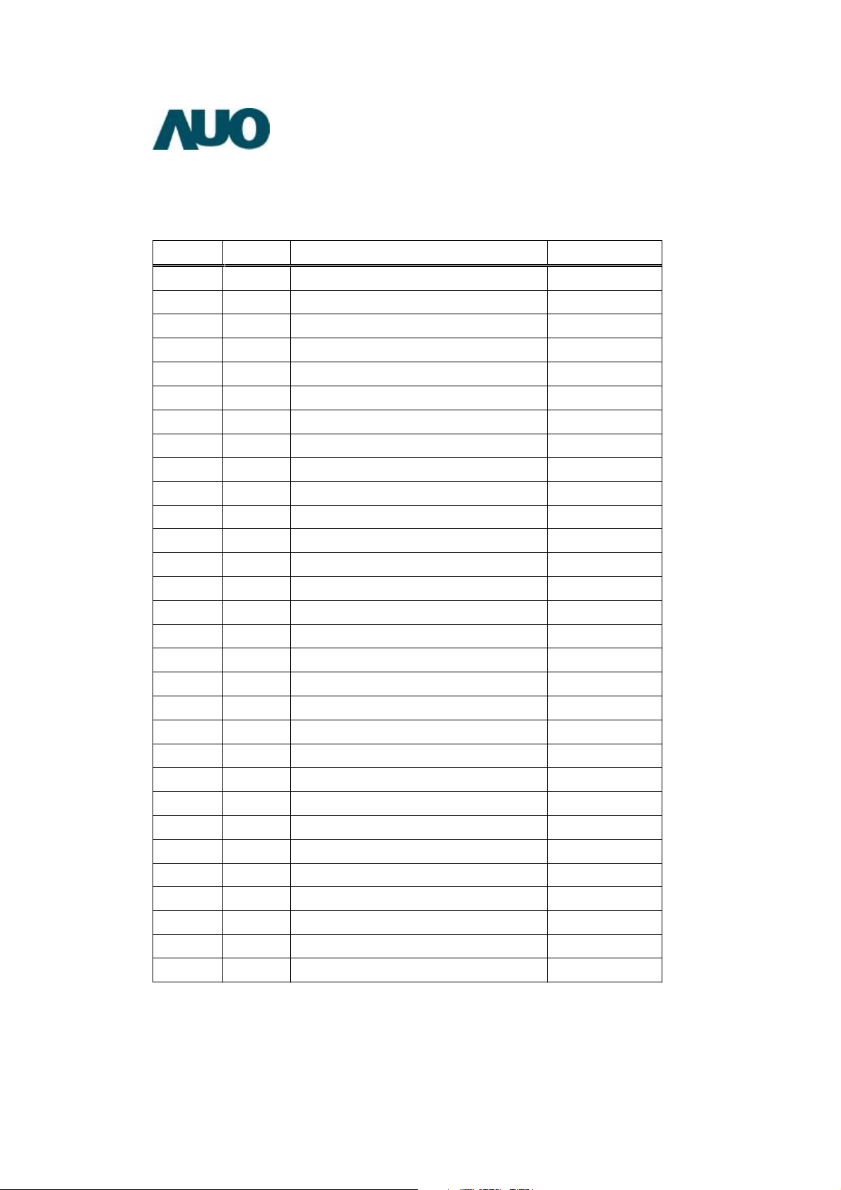
3-2 Interface Connections
- LCD connector (CN3): JAE FI-E30S or equivalent.
- LVDS Transmitter: DS90C385 (NS) or equivalent
Pin No Symbol Description note
1 Re served Open or High Auo int ernal test pin
2 Re served Open or High Auo int ernal test pin
3 Re served Open or High Auo int ernal test pin
4 GND Ground and Signal Return
5 RIN0- LVDS Channel 0 negative
6 RIN0+ LVDS Cha nnel 0 posi tive
7 GND Ground and Signal Return for LVDS
8 RIN1- LVDS Channel 1 negative
9 RIN1+ LVDS Cha nnel 1 posi tive
10 GND Ground and Signal Return for LVDS
11 RIN2- LVDS Channel 2 negative
12 RIN2+ LVDS Cha nnel 2 positi ve
13 GND Ground and Signal Return for LVDS
14 RCLK- LVDS Clock negative
15 RCLK+ LVDS Clock positive
16 GND Ground and Signal Return for LVDS
17 RIN3- LVDS Channel 3 negative
18 RIN3+ LVDS Cha nnel 3 positi ve
19 GND Ground and Signal Return
20 Reserved Open or High Auo internal test pin
21 LVDS Option Low for JEIDA, High/Open for NS
22 Reserved Open
23 GND Ground and Signal Return
24 GND Ground and Signal Return
25 GND Ground and Signal Return
26 Vcc 5V, DC, Regulated
27 Vcc 5V, DC, Regulated
28 Vcc 5V, DC, Regulated
29 Vcc 5V, DC, Regulated
30 Vcc 5V, DC, Regulated
Note:
1. All GND (ground) pins should be connected together and should also be connected to the LCD’s metal
frame. All Vcc (power input) pins should be connected together.
©Copyright AU Optronics, Inc.
January, 2003 All Rights Reserved. T315XW02 VC - Specs. ver 1 9/28
No Reproduction and Redistribution Allowed
Page 25
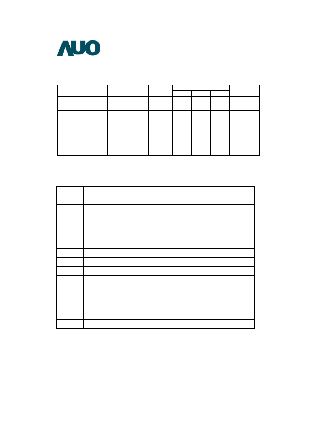
BACKLIGHT CONNECTOR PIN CONFIGURATION -
1. Electrical specification
Spec
Min Typ Max
Input Voltage --- 21.6 24.0 26 .4 VDC
Input Current (Stable Condition )
Input Power (Stable Condition)
Inrush Current
On/Off Control Voltage VBLON VDC
On/Off Control Current IBLON VDDB=24 V 0.0 --- 1.5 mADC
Dimming Control Current VDIM VDC
Note1 : VDIM= 3.3V (MAX) Ta =25 ±5 , Turn on for 45minute s
Note 2 : Measurement condition Rising time = 20 ms (VDDB : 10 %~90%) ;
VDDB
IDDB
PDDB
IRUSH
VDDB=24V
VDDB=24V
VDDB=24V
ON VDDB=24V 2.0 --- 5.0
OFF VDDB=24V 0.0 --- 0.8
MAX VDDB=24V --- 3.3 ---
MIN VDDB= 24V --- 0.0 ---
4.35 4.60 4.85 ADC
109 115 121 W
--- --- 6.0 ADC
UnitConditionItem Symb.
2. Input specification
CN1: JST PHR-14 or equivalent
No Symbol Description
1 VDDB (Main Power) DC input 24.0 VDC
2 VDDB (Main Power) DC input 24.0 VDC
3 VDDB (Main Power) DC input 24.0 VDC
4 VDDB (Main Power) DC input 24.0 VDC
Note
1
1
1,2
5 VDDB (Main Power) DC input 24.0 VDC
6 GND Ground
7 GND Ground
8 GND Ground
9 GND Ground
10 GND Ground
11 Reserved Please leave it Open.
12 VBLON (Enable Pin) On/Off control Signal; High: On; Low: Off
13 VDIM (LC D Bright) Internal PWM Dimming control signal input (DC 0~3.3V)
(3.3V : Maximum brightness, 0V min brightness)
14
Reserved Pl ease leave it Open.
©Copyright AU Optronics, Inc.
January, 2003 All Rights Reserved. T315XW02 VC - Specs. Ver 1 11/28
No Reproduction and Redistribution Allowed
Page 26
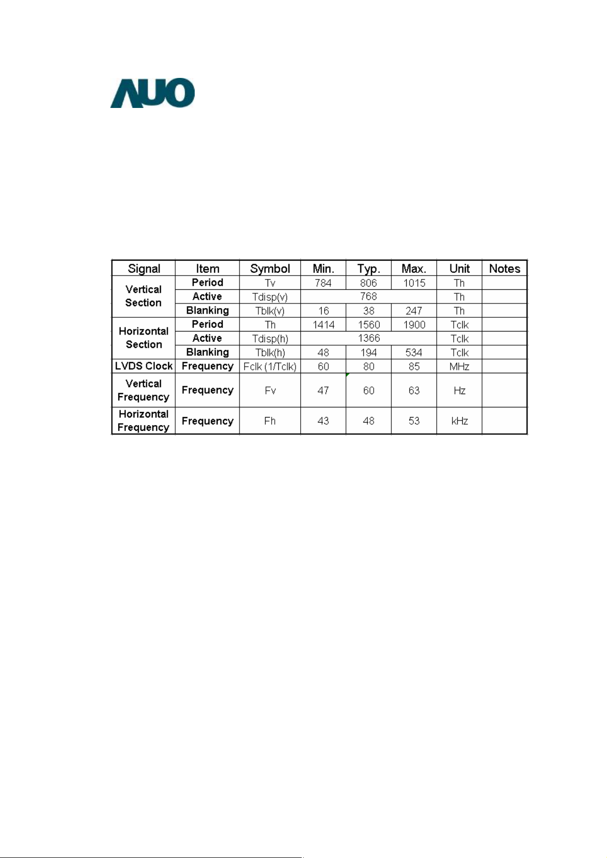
3-3 Signal Timing Specifications
This is the signal timing required at the input of the User connector. All of the interface signal timing should be
satisfied with the following specifications for it’s proper operation.
* Timing Table
DE only Mode
Vertical Frequency:
Notes:
1.) Display position is specific by the rise of DE signal only.
Horizontal display position is specified by the rising edge of 1
st
DCLK after the rise of 1stDE, is displayed on
the left edge of the screen.
Vertical display position is specified by the rise of DE after a “Low” level period equivalent to eight times of
horizontal period. The 1
st
data corresponding to one horizontal line after the rise the of 1stDE is displayed at the
top line of screen.
3.) If a period of DE “High” is less than 1366 DCLK or less than 768 lines, the rest of the screen displays black.
4.) The display position does not fit to the screen if a period of DE “High” and the effective data period do not
synchronize with each other.
©Copyright AU Optronics, Inc.
January, 2003 All Rights Reserved. T315XW02 VC - Specs. ver 1 12/28
No Reproduction and Redistribution Allowed
Page 27
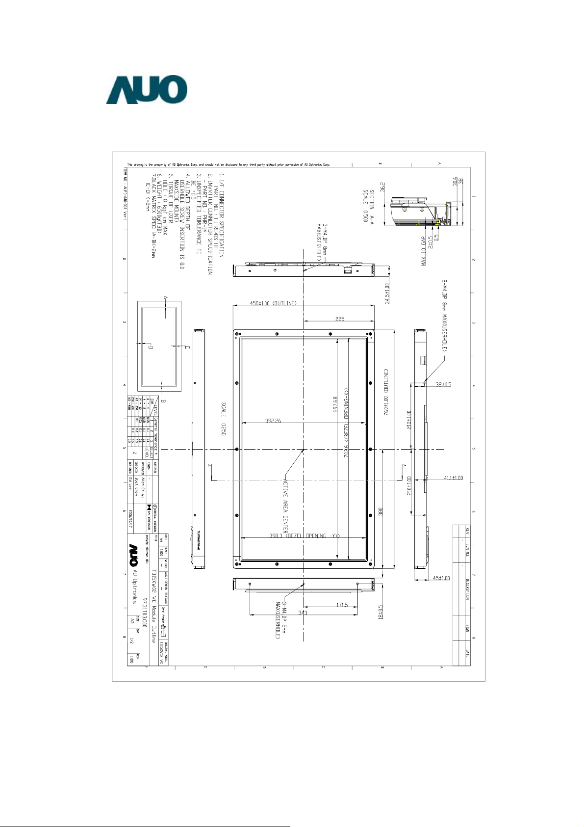
Front:
©Copyright AU Optronics, Inc.
January, 2003 All Rights Reserved. T315XW02 VC - Specs. Ver 0 21/28
No Reproduction and Redistribution Allowed
Page 28
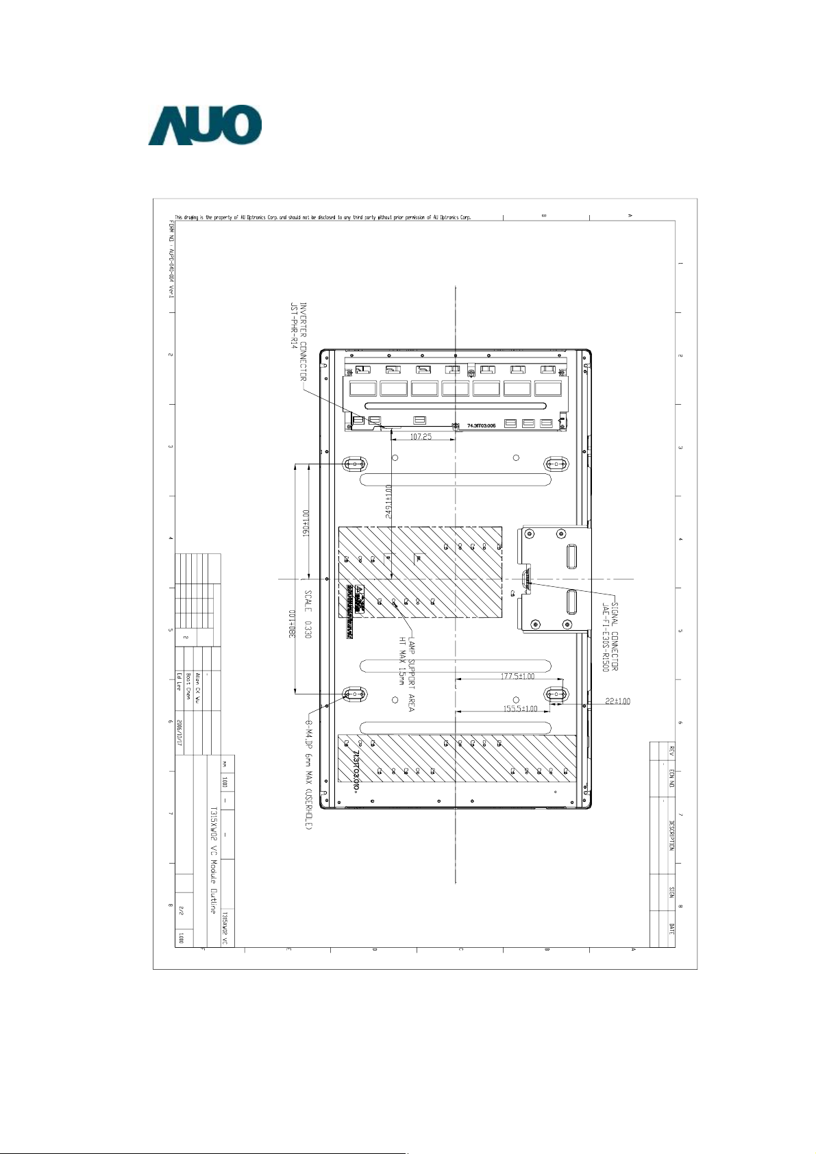
Back:
©Copyright AU Optronics, Inc.
January, 2003 All Rights Reserved. T315XW02 VC - Specs. Ver 1 22/28
No Reproduction and Redistribution Allowed
Page 29
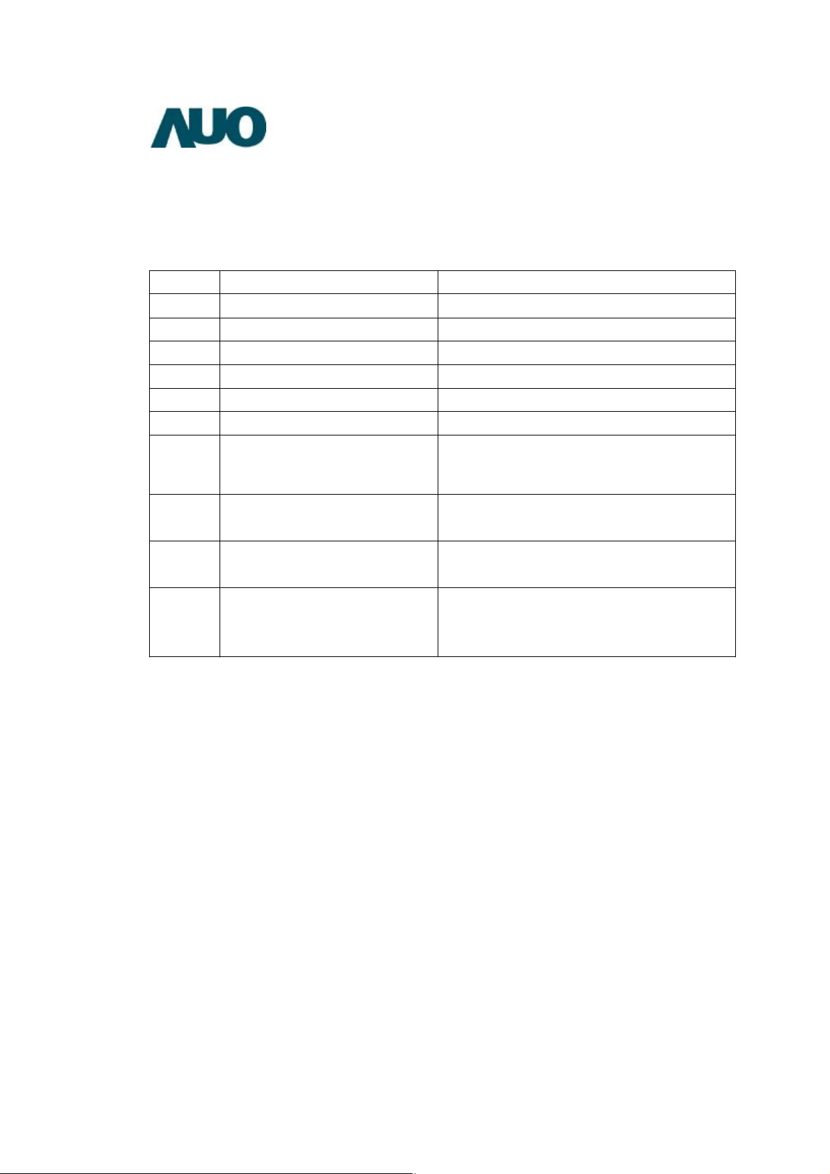
6. Reliability:
Environment test condition
No Test Item Condition
1 High temperature storage test
2 Low temperature storage test
3 High temperature operation test
4 Low temperature operation test
5 Thermal Humidity Bias Test
6 Thermal Shock Test
7 Vibration test
(non-operating)
8 Shock test
(non-operating)
9 Vibration test
(with carton)
10 Drop test
(with carton)
Ta=60 Determination:300h
Ta =- 2 0 Determination:300h
Ta=50 Determination:300h
Ta=-5 Determination:300h
Ta=50 80%RH Determination:300h
Ta =- 2 0/0.5h~60/0.5h Determination:500cycles
Wave form: random
Vibration level : 1.0G RMS
Bandwidth : 10-500Hz
Duration: X, Y, Z 20min, one time each direction
Shock level: 50G
Waveform: half since wave, 11ms
Direction: X, Y, Z, one time each direction
Random wave Vibration:10~200Hz,1.5Grms,30minutes
Direction: X, Y, Z, one time each direction
Height: 53.3cm
1 corner, 3 edges, 6 surfaces
(ASTMD4169-I)
©Copyright AU Optronics, Inc.
January, 2003 All Rights Reserved. T315XW02 VC - Specs. Ver 1 23/28
No Reproduction and Redistribution Allowed
Page 30
Page 31

7. International Standard
7-1. Safety
(1) UL1950 Third Edition, Underwriters Laboratories, Inc. Jan. 28, 1995
Standard for Safety of Information Technology Equipment Including electrical Business Equipment.
(2) CAN/CSA C22.2 No. 950-95/60950 Third Edition, Canadian Standards Association,
Standard for Safety of Information Technology Equipment Including Electrical Business Equipment.
(3) EN60950 : 1992+A2: 1993+A2: 1993+C3: 1995+A4: 1997+A11: 1997
IEC 950: 1991+A1: 1992+A2: 1993+C3: 1995+A4:1996
European Committee for Electrotechnical Standardization (CENELEC)
EUROPEAN STANDARD for Safety of Information Technology Equipment Including Electrical
Business Equipment.
7-2. EMC
a) ANSI C63.4 “Methods of Measurement of Radio-Noise Emissions from Low-Voltage Electrical and
Electrical Equipment in the Range of 9kHz to 40GHz. “American National standards Institute(ANSI),
1992
b) C.I.S.P.R “Limits and Methods of Measurement of Radio Interface Characteristics of Information
Technology Equipment.” International Special committee on Radio Interference.
c) EN 55022 “Limits and Methods of Measurement of Radio Interface Characteristics of Information
Technology Equipment.” European Committee for Electrotechnical Standardization. (CENELEC),
1998
©Copyright AU Optronics, Inc.
January, 2003 All Rights Reserved. T315XW02 VC - Specs. Ver 0 24/28
No Reproduction and Redistribution Allowed
Page 32
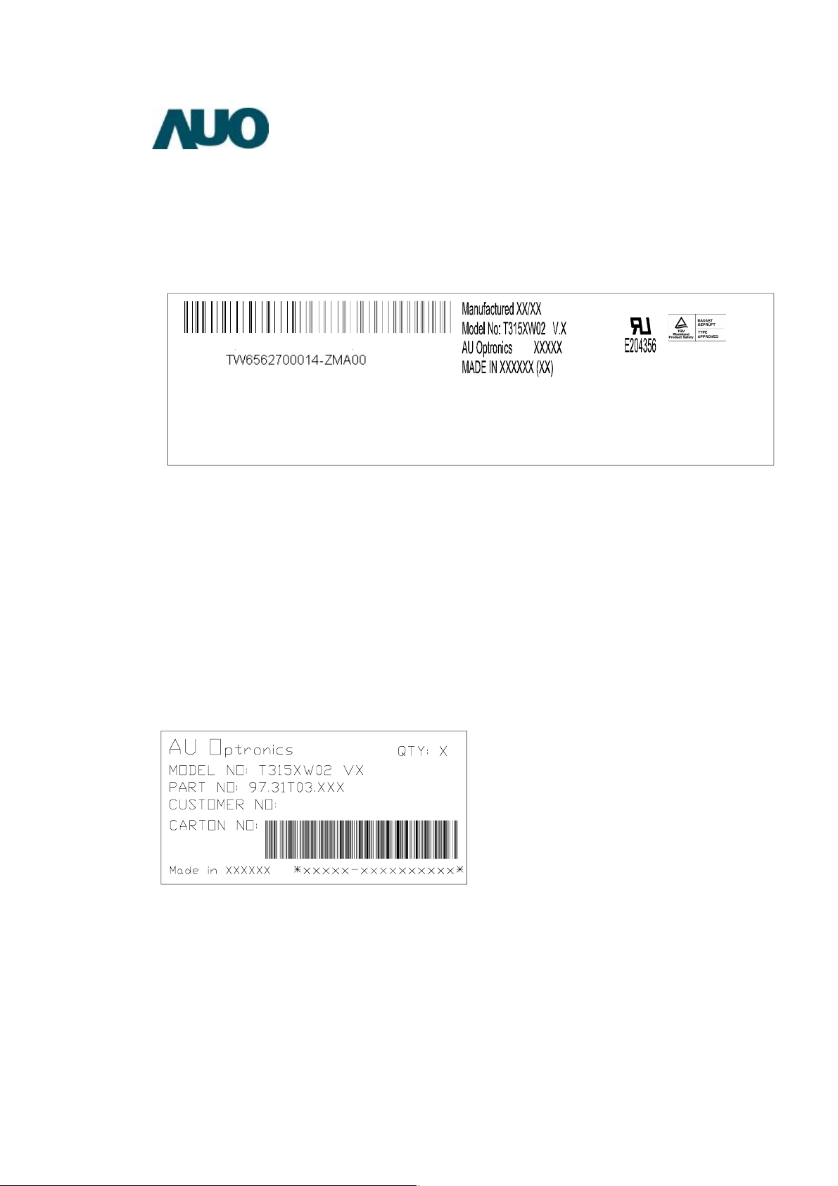
8. Packing
Panel label:
TW6562700014
TW65627: Production Lot
00014: Panel Serial Number
ZMA: AUO internal code
Manufactured 06/21: 2006 week 21
Made In Taiwan: Taiwan made
CUS
Carton Label :
©Copyright AU Optronics, Inc.
January, 2003 All Rights Reserved. T315XW02 VC - Specs. Ver 0 25/28
No Reproduction and Redistribution Allowed
 Loading...