

Page 1
DMF6104NF-FW (AE) No.97-0106 OPTREX CORPORATION Page 1/17
OPTREX
Type No.
*******
April 25, 1997
First Edition
Final Revision
Quality Assurance Div.
Production Div.
Checked by
Checked by
Approved by
Production Div.
Design Engineering Div.
Prepared by
LCD Module Specification
DMF6104NF-FW
DMF6104NF-FWDMF6104NF-FW
DMF6104NF-FW
Table of Contents
1. General Specifications.............................................................................2
2. Electrical Specifications...........................................................................3
3. Optical Specifications..............................................................................8
4. I/O Terminal...........................................................................................10
5. Test..........................................................................................................12
6. Appearance Standards............................................................................13
7. Code System of Production Lot..........................................................16
8. Type Number .........................................................................................16
9. Applying Precautions.............................................................................16
10. Handling Precautions.............................................................................17
Revision History
Rev. Date Page Comment
Page 2
DMF6104NF-FW (AE) No.97-0106 OPTREX CORPORATION Page 2/17
OPTREX
1.General Specifications
Operating Temp.
:
min. 10℃ ~ max. 40℃
Storage Temp.
:
min. -20℃ ~ max. 60℃
Dot Pixels
:
256 (W) × 128 (H) dots
Dot Size
:
0.43 (W) × 0.43 (H) mm
Dot Pitch
:
0.47 (W) × 0.47 (H) mm
Viewing Area
:
127.0 (W) × 70.0 (H) mm
Outline Dimensions
:
167.0 (W) × 116.0 (H) × 24.0 (D) mm
W eight
:
250g max.
LCD Type
:
NTD-7451
( F-STN / Black
&White-mode / Transmissive )
Viewing Angle
:
6:00
Data Transfer
:
4-bit parallel data transfer
Backlight
:
Cold Cathode Fluorescent Lamp (CFL) × 1
Drawings
:
Dimensional Outline UE-32050B
Page 3
DMF6104NF-FW (AE) No.97-0106 OPTREX CORPORATION Page 3/17
OPTREX
2.Electrical Specifications
2.1.Absolute Maximum Ratings
V
SS
=0V
Parameter Symbol Conditions Min. Max. Units
Supply Voltage
(Logic)
VCC-VSS
-
-0.3 6.0 V
Supply Voltage
(LCD Drive)
VCC-VEE
-
0 30.0 V
Input Voltage VI
-
-0.3 VCC+0.3 V
2.2.DC Characteristics
Ta=25℃, V
SS
=0V
Parameter Symbol Conditions Min. Typ. Max. Units
Supply Voltage
(Logic)
VCC-VSS
-
4.5 - 5.5 V
Supply Voltage
(LCD Drive)
VCC-VEE Shown in 3.1 V
High Level
Input Voltage
VIH VCC=5.0V±10% 0.8×VCC
-
V
CC
V
Low Level
Input Voltage
VIL VCC=5.0V±10% 0 - 0.2×VCC V
High Level
Output Voltage
VOH IOH=-0.2mA VCC-0.4
-
V
CC
V
Low Level
Output Voltage
VOL IOL=0.2mA 0 - 0.4 V
Supply Current
ICC VCC-VSS=5.0V
-
5.0 20.0 mA
I
EE
VCC-VEE=13.3V
-
4.7 15.0 mA
Page 4
DMF6104NF-FW (AE) No.97-0106 OPTREX CORPORATION Page 4/17
OPTREX
2.3.AC Characteristics
V
CC
=5.0V±10%
Parameter Symbol Min. Max. Units
Clock Pulse Width
t
WC
100 - ns
Latch Pulse High Level Width
t
WL
125 - ns
Clock Pulse Rise/Fall Time
t
r, tf
-
50 ns
CP→LP Rise Time
t
CL
63 - ns
CP→LP Fall Time
t
LSU2
90 - ns
LP→CP Rise Time
t
LSU1
90 - ns
LP→CP Fall Time
t
LC
63 - ns
Data Setup Time
t
DSU
50 - ns
Data Hold Time
t
DHD
80 - ns
FLM Data Setup Time
t
SETUP
100 - ns
FLM Data Hold Time
t
HOLD
100 - ns
t
HOLD
t
SETUP
t
r
t
f
t
DHD
t
DSU
t
WC
t
LC
t
LSU2
CP
t
CL
t
LSU1
LP
FLM
D0~D3
t
WL
t
WC
Page 5
DMF6104NF-FW (AE) No.97-0106 OPTREX CORPORATION Page 5/17
OPTREX
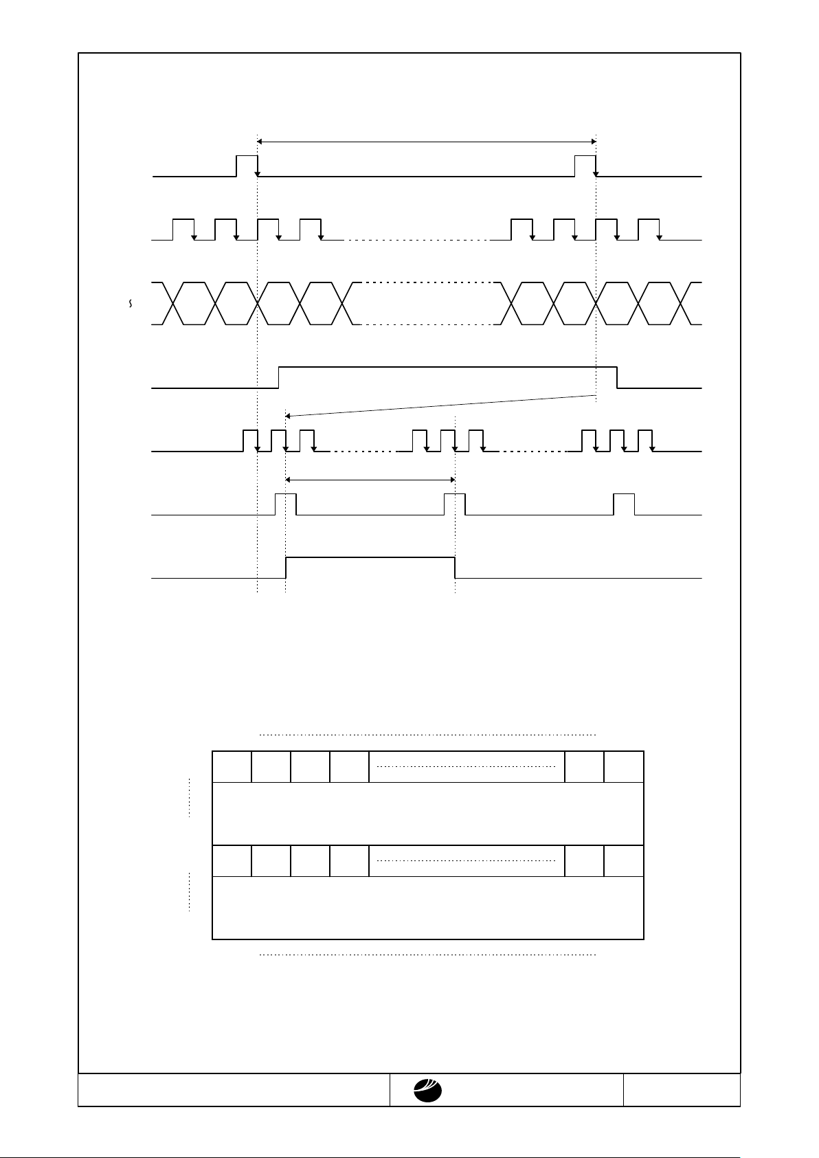
2.4.Timing Chart
2.5.Comparison of Display and Data
T=0.223ms typ.
64×T
FLM
(Reduction)
(Reduction)
LP
FLM
M
D3
D0
CP
LP
~
#1 + #65 DATA
SEGSEG SEGSEG SEGSEG SEGSEG
512508 84512508 84
509
~
505
~
5
~
1
~
509
~
505
~
5
~
1
~
SEG1 SEG256
#65
#1
#64
#128
D2D3
D0~D3
D0~D3
SEG257 SEG512
D0D1 D0D1
D2D3 D0D1 D0D1
Page 6
DMF6104NF-FW (AE) No.97-0106 OPTREX CORPORATION Page 6/17
OPTREX
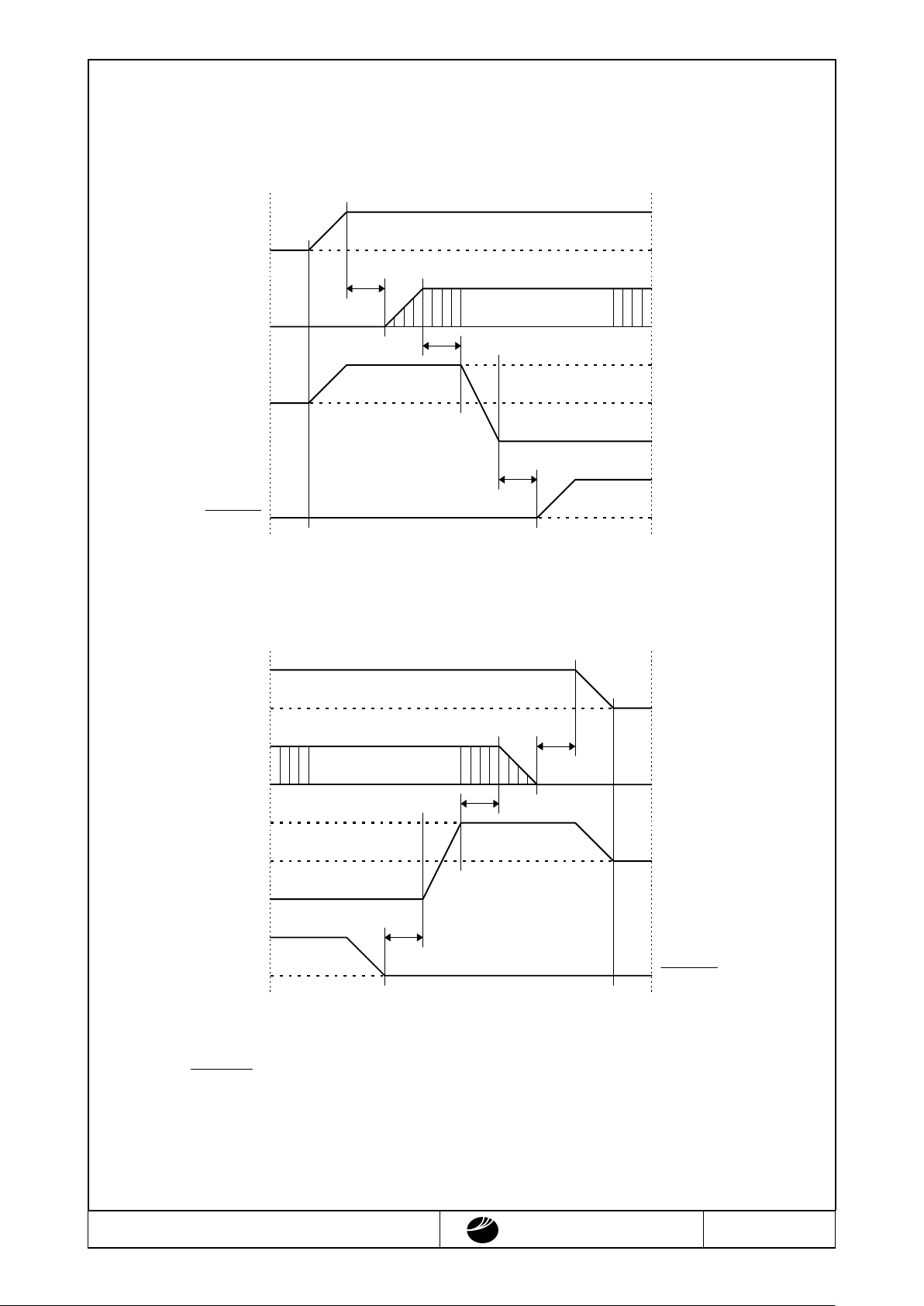
2.6.Power Supply ON/OFF Sequence
2.6.1.ON Sequence
2.6.2.OFF Sequence
Please maintain the above sequence when turning on and off the power supply of the module.
If DISPOFF is supplied to the module
w
hile alternate signal for LCD driving (M) is unstable,
DC component will be supplied to the LCD panel. This may cause damage the LCD module.
VCC
VSS
VEE
VSS
VSS
VCC
VSS
VCC
DISPOFF
VEE
VCC
0≦t
0≦t
SIGNAL
SIGNAL
LEVEL
VCC
0≦t
VCC
VSS
VEE
VSS
VSS
VCC
VSS
VCC
DISPOFF
VEE
VCC
0≦t
0≦t
SIGNAL
SIGNAL
LEVEL
VCC
0≦t
Page 7

DMF6104NF-FW (AE) No.97-0106 OPTREX CORPORATION Page 7/17
OPTREX
2.7.Lighting Specifications
Ta=25℃
Parameter Symbol Conditions Min. Typ. Max. Units Notes
Lamp Voltage VL
-
-
250 - Vrms 1
Lamp Current IL
-
4.0 5.0 6.0 mArms 2
Starting Voltage VS
-
600 -
-
Vrms 3
Surface Luminance L IL=5.0mA 50 -
-
cd/㎡ 4
Average Life TAL I
L
=5.0mA
-
20000 - hrs 5
Note 1 : The voltage ( r.m.s. ) to maintain the electric discharge of the lamp. It is measured after lighting for
3 minutes .
Note 2 : The current ( r.m.s. ) to flow through the lamp with the electric discharge. It i s mea s ured after
lighting for 3 minutes .
Note 3 : The voltage at starting the electric discharge when the voltage is increased gradually from 0V.
Note 4 : Surface Luminance is specified by the initial data of luminance measured at the center of display
surface after 20 minutes power on. ( All ON pattern )
Note 5 : CFL life is defined as the time for which the initial luminance is attenuated by 50% of the
luminance value. Average Life representes the time elapsed at the point of time when the residual
ratio becomes below 50% when plural lamps are lighted in comparison with the definition of life
mentioned above.
V
N
I
CFL Testing Circuit
L
F
C
VS VL
IL
Page 8

DMF6104NF-FW (AE) No.97-0106 OPTREX CORPORATION Page 8/17
OPTREX
3.Optical Specifications
3.1.LCD Driving Voltage
Parameter Symbol Conditions Min. Typ. Max. Units
Recommended Ta=10℃
-
-
15.1 V
LCD Driving Voltage VCC-VEE Ta=25℃ 12.4 13.3 14.2 V
Note 1 Ta=40℃ 11.7 -
-
V
Note 1 : Voltage (Applied actual waveform to LCD Module) for the best contrast. The range of
minimum and maximum shows tolerance of the operating voltage. The specified contrast ratio and
response time are not guaranteed over the entire range.
3.2.Optical Characteristics
Ta=25℃, 1/64 Duty, 1/9 Bias, V
D
=13.3V (Note 4), θ= 0゚, φ=-゚
Parameter Symbol Conditions Min. Typ. Max. Units
Contrast Ratio Note 1 CR
θ
= 0゚, φ=-゚
-
15 -
Viewing Angle Shown in 3.3
Response Rise Note 2
τ
r
-
-
110 200 ms
Time Decay Note 3
τ
d
-
-
160 240 ms
Note 1 : Contrast ratio is definded as follows.
CR = L
ON
/ L
OFF
L
ON
: Luminance of the ON segments
L
OFF
: Luminance of the OFF segments
Note 2 : The time that the luminance level reaches 90% of the saturation level from 0% when ON
signal is applied.
Note 3 : The time that the luminance level reaches 10% of the saturation level from 100% when OFF
signal is applied.
Note 4 : Definition of Driving Voltage V
D
Assuming that the typical driving waveforms shown below are applied to the LCD Panel at
1/A Duty - 1/B Bias ( A : Duty Number, B : Bias Number ). Driving voltage V
D
is definded
as the voltage V
O-P
when the contrast ratio (CR=LON / L
OFF
) is at its maximum.
V
O-P
1 /
f
F
(
B-2
)
×
V
O-P
/ B
1 /
(
f
F
×
A
)
〈
OFF SIGNAL
〉
〈
ON SIGNAL
〉
Page 9

DMF6104NF-FW (AE) No.97-0106 OPTREX CORPORATION Page 9/17
OPTREX
3.3.Definition of Viewing Angle and Optimum Viewing Area
・
Point ● shows the point where contrast ratio is measured. : θ= 0゚, φ=-゚
・
Driving condition : 1/64 Duty, 1/9 Bias, V
D
=13.3V,
f
F
=70Hz
・
Area shows typ. CR≧2
3.4.System Block Diagram
0
゚
90
゚
180
゚
270
゚
θ
φ
270
゚
135
゚
315
゚
225
゚
45
゚
180
゚
90
゚
θ
(φ= 0
゚)
φ
10 20 30 40 50
φ
Halogen bulb
Computer
Rotation Table (θ,φ)
Temperature Chamber
LCD
Optical Fiber
Waveform Generator
Control Unit &
#1980A WB
Photometer
θ
Page 10

DMF6104NF-FW (AE) No.97-0106 OPTREX CORPORATION Page 10/17
OPTREX
4.I/O Terminal
4.1.Pin Assignment
No. Symbol Level Function
1
V
CC
―
Power Supply for Logic
2
V
SS
―
Power Supply (0V, GND)
3
V
EE
―
Power Supply for LCD Drive
4
LP H→L Data Latch Signal
5
M H / L Alternate Signal for LCD Drive
6
DISPOFF H / L Display Control Signal H : Display on L : Display off
7
NC - Non-connection
8
FLM H / L First Line Marker
9
CP H→L Clock Signal for Shifting Data
10
NC - Non-connection
11
D0 H / L Display Data
12
D1 H / L Display Data
13
D2 H / L Display Data
14
D3 H / L Display Data
15
FL - Power Supply for CFL (HOT)
16
FL (GND) - Power Supply for CFL (GND)
4.2.Example of Power Supply
It is recommended to apply a potentiometer for the contrast adjust due to the tolerance
of the driving voltage and its temperature dependence.
VSS
MODULE
VEE
VCC
VEE (-Voltage)
VCC (+Voltage)
Tr=2SA1202 or equivalent
R1+R2+VR=10~20K
Ω
VSS (0V)
R2
R1
VR
Tr
Page 11

DMF6104NF-FW (AE) No.97-0106 OPTREX CORPORATION Page 11/17
OPTREX
4.3.Block Diagram
FL (GND)
FL
VEE
VSS
VCC
D0~D3
M
FLM
LP
DISPOFF
CP
or equivalent
MSM5298 × 1
Row Driver
or equivalent
MSM5299 × 4
Column Driver
L C D P
256
64
4
256 × 128 dots
To LSIBias Circuit
CFL Backlight
or equivalent
MSM5299 × 3
Column Driver
240
64
4
16
Page 12

DMF6104NF-FW (AE) No.97-0106 OPTREX CORPORATION Page 12/17
OPTREX
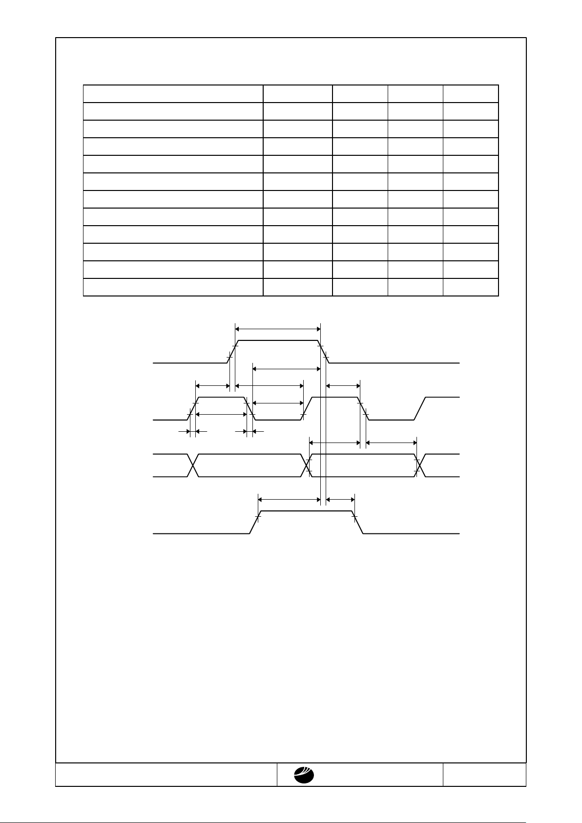
5.Test
No change on display and in operation under the following test condition.
No. Parameter Conditions Notes
1 High Temperature Operating 40
℃±2℃
, 96hrs (operation state)
2 Low Temperature Operating 10
℃±2℃
, 96hrs (operation state) 3
3 High Temperature Storage 60
℃±2℃
, 96hrs 4
4 Low Temperature Storage -20
℃±2℃
, 96hrs 3, 4
5 Damp Proof Test 40
℃±2℃
, 90~95%RH, 96hrs 3, 4
6 Vibration Test Total fixed amplitude : 1.5mm 5
Vibration Frequency : 10~55Hz
One cycle 60 seconds to 3 directions of X, Y, Z for
each 15 minutes
7 Shock Test To be measured after dropping from 60cm high on
the concrete surface in packing state.
Note 1 : Unless otherwise specified, tests will be conducted under the following condition.
Temperature : 20±5℃
Humidity : 65±5%
Note 2 : Unless otherwise specified, tests will be not conducted under functioning state.
Note 3 : No dew condensation to be observed.
Note 4 : The function test shall be conducted after 4 hours storage at the normal temperature and humidity
after removed from the test chamber.
Note 5 : Vibration test will be conducted to the product itself without putting it in a container.
E
A
G
D
C
F
60cm
Con crete Surface
Dropping method corner dropping
E,F,G face : once
B,C,D edge : once
A corner : once
Face dropping
Edge dropping
B
Page 13

DMF6104NF-FW (AE) No.97-0106 OPTREX CORPORATION Page 13/17
OPTREX
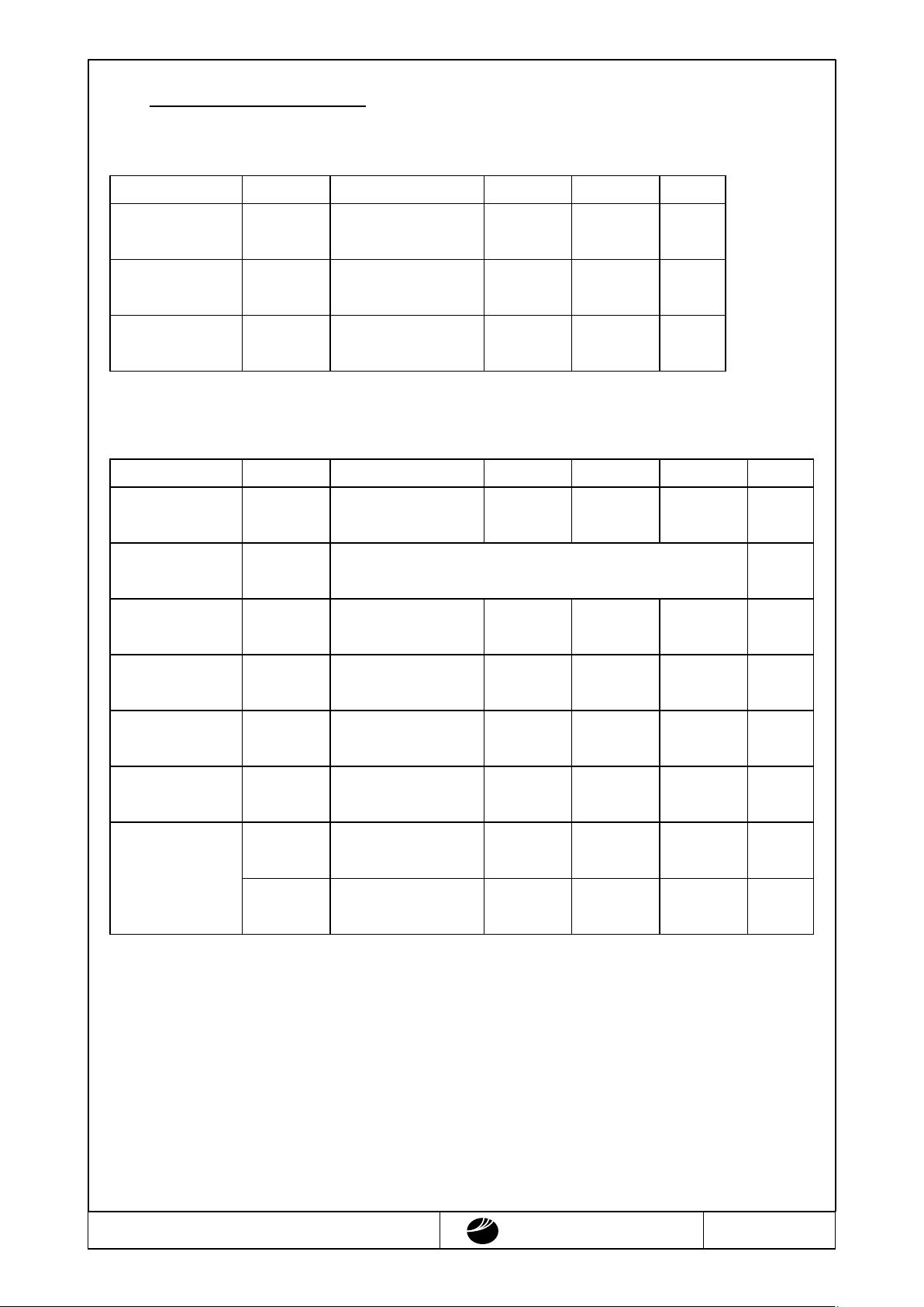
6.Appearance Standards
6.1.Inspection conditions
The LCD shall be inspected under 40W white fluorescent light.
The distance between the eyes and the sample shall be more than 30cm.
All directions for inspecting the sample should be within 45゚against perpendicular line.
6.2.Definition of applicable Zones
A Zone : Active display area
B Zone : Area from outside of "A Zone" to validity viewing area
C Zone : Rest parts
A Zone + B Zone = Validity viewing area
A Zone
B Zone
C Zone
Bezel Flame
45
゚
Page 14

DMF6104NF-FW (AE) No.97-0106 OPTREX CORPORATION Page 14/17
OPTREX
6.3.Standards
No. Parameter Criteria
1 Black and (1) Round Shape
White Spots, Zone Acceptable Number
Foreign Substances Dimension (mm) A B C
D ≦0.1 * * *
0.1
<
D ≦0.2 3 5 *
0.2
<
D ≦0.25 2 3 *
0.25< D ≦0.3 0 1 *
0.3
<
D 0 0 *
D = ( Long + Short ) / 2 * : Disregard
(2) Line Shape
Zone Acceptable Number
X (mm) Y (mm) A B C
- 0.03≧W * * *
2.0≧L 0.05≧W 3 3 *
1.0≧L 0.1 ≧W 3 3 *
- 0.1 <W In the same way (1)
X : Length Y : Width * : Disregard
Total defects shall not exceed 5.
2 Air Bubbles
(between glass Zone Acceptable Number
& polari zer) Dimension (mm) A B C
D ≦ 0.3 * * *
0.3
<
D ≦ 0.4 3 * *
0.4
<
D ≦ 0.6 2 3 *
0.6
<
D 0 0 *
* : Disregard
Total defects shall not exceed 3.
Page 15

DMF6104NF-FW (AE) No.97-0106 OPTREX CORPORATION Page 15/17
OPTREX
No. Parameter Criteria
3 The Shape of Dot (1) Dot Shape (with Dent)
As per the sketch of left hand.
(2) Dot Shape (with Projection)
Should not be connected to next dot.
(3) Pin Hole
(X+Y) / 2≦0.2mm
(Less than 0.1mm is no counted.)
(4) Deformation
(X+Y) / 2≦0.2mm
Total acceptable number : 1/dot, 5/cell
(Defect number of (4) : 1pc.)
4 Polarizer Scratches Refer to the sample.
5
Polarizer Dirts If the stains are removed easily from LCDP surface, the module is not
defective.
6
Complex Foreign Black spots, line shaped foreign substances or air bubbles between
Substance Defects glass & polarizer should be 5pcs maximum in total.
7
Distance between D≦0.2 : 20mm or more
Different Foreign 0.2<D : 40mm or more
Substance Defects
0.15
≧
Y
X
X
Y
Page 16

DMF6104NF-FW (AE) No.97-0106 OPTREX CORPORATION Page 16/17
OPTREX
7.Code System of Production Lot
The production lot of module is specified as follows :
□
□
□ □ □ □
Factory Number
Factory Code (Alphabet)
Production Week (1~5)
Producti on Month (1~9, X, Y, Z)
Production Year (Lower 2 digits)
8.Type Number
The type number of module is specified on the back of module as follows :
DMF6104N
F-FW
Stamp
Etching or Printing
9.Applying Precautions
Please contact us when questions and/or new problems not specified in this specifications arise.
Page 17

DMF6104NF-FW (AE) No.97-0106 OPTREX CORPORATION Page 17/17
OPTREX
10.Handling Precautions
Operex Products are designed for use in ordinary electronic devices such as business machines,
telecommunications equipment, measurement devices and etc..
Optrex Products are not designed, intended, or authorized for use in any application in which the failure of
the product could result in a situation where personal injury or death may occur. These applications
include, but are not limited to, life-sustaining equipment, nuclear control devices, aerospace equipment,
devices related to hazardous or flammable materials, etc. (If Buyer intends to purchase or use the Optrex
Products for such unintended or unauthorized applications, Buyer must secure prior written consent to
such use by a responsible officer of Optrex Corporation.) Should Buyer purchase or use Optrex Products
for any such unintended or unauthorized application (without such consent), Buyer shall indemnify and
hold Optrex and its officers, employees, subsidiaries, affiliates and distributors harmless against all claims,
costs, damages and expenses, and reasonable attorney's fees, arising out of, directly or indirectly, any
claim of personal injury or death associated with such unintended or unauthorized use, even if such claim
alleges that Optrex was negligent regar ding the design or manufacture of the part.
1) LCD may be broken because it is made of glass.
2) Polarizer is a soft material and can easily be scratched.
3) Please avoid static electricity.
①
Please be sure to ground human body and electric appliances during work.
②
It is preferable to use conductive mat on table and wear cotton clothes or conduction processed fiber.
Synthetic fiber is no t recommended.
③
Please slowly peel off protective film, because static electricity may be charged.
4) If it is necessary to store LCD modules for a long time, please comply with the following procedures.
If storage condition is not satisfactory, display (especially polarizer) may be deteriorated or soldering
I/O terminals may become difficult (some oxide is generated at I/O terminals plating).
①
Store as delivered by Optrex
②
If you store as unpacked, put in anti-static bag, seal its opening and store where it is not subjected to
direct sunshine nor fluorescent l amp.
③
Store at temperature 0 to +35℃ and at low humidity. Please refer to our specification sheets for
storage temperature range and humidity condition.
5) The module does not contain excess current limiter.
Please design the limiter to cut excess current in your power supply circuit.
6) Liquid crystal may be leaked when display is broken. Never taste it. If your hands or clothes touch it,
please immediately wash using soap.
7) The connection between the bezel and V
SS
(GND) is not specified in the module.
(Some module do not maintain connection between them.)
Please consult OPTREX to specify the connection.
8) A high voltage over 1000V is applied at the connector of CFL cable when the CFL inverter is
connected and energized. Please do not touch there incidentally or accidentally to avoid a skin burn.
And please set the cable properly in the housing to avoid a worn-out of isolated cover of cable wire.
Optrex shall not be responsible for any infringement of industrial property rights of third parties in any
country arising out of the application or use of Optrex Products, except which directly concern the
structure or production of such products.
 Loading...