

Page 1

1
8Bit Single Chip Microcontroller DMC73C167
1. Introduction
1.1 Description
2
1.2 Pin Configurations
2
1.3 Features
3
2. Device Functions
2.1 Block Diagram
5
2.2 Pin Description
6
3. Electrical Specifications
3.1 Absolute Maximum Ratings
8
3.2 Recommended operating conditions
9
3.3 Electrical characteristics
10
3.4 AC Charcteristics
11
3.5 I/O Circuits
14
4. Architecture
4.1 Overview
16
4.2 Register File
16
4.3 Peripheral File (PF)
17
4.4 Stack Pointer (SP)
18
4.5 Status Register (ST)
18
4.6 Program Counter (PC)
19
4.7 Peripheral File Map
19
4.8 Interrupt and Reset Priorities
22
5. Function
5.1 Input/Output Ports
24
5.2 Device Initialization 28
5.3 I/O Control Register 28
5.4 Interrupt Logic and External Interrupt 34
5.5 Programmable Timer / Event Counter
37
5.6 A/D Converter
45
5.7 I2C
49
5.8 6-bit PWM (PWM1_0, PWM1_8)
63
5.9 14-bit PWM (PWM0)
68
5.10 On Screen Display
73
6. OTP Deivce Specifications
6.1 Pin Assignment of OTP programming Adapter Board
83
6.2 Package Descriptions (Mechanical Data)
88
* Appendix : OSD Font Design Guide
89
Table of Contents
£Ä£Á£Å£×£Ï£Ï
DAEWOO ELECTRONICS CO., LTD.
Page 2
2
8Bit Single Chip Microcontroller
DMC73C167
1. INTRODUCTION
1.1 Description
The DMC73C167 is an 8-bit CMOS microcontroller with 16K bytes of on-chip ROM, 256
bytes of on-chip RAM, OSD (On Screen Display), A/D converter, 10 PWM output ports,
three timers, multi-master I2C communications port, 8 output only pins, and 20 normal I/O
pins. The high-performance CPU internal peripherals allow flexible design in industrial
equipment, televisions, camcorders, VCRs, and other home appliances.
1.2 Pin Configurations
PWM0 (14bit) 1 54 VCC
PWM1_0 (6bit) 2 53 A7
PWM1_1 (6bit) 3 52 SCL
PWM1_2 (6bit) 4 51 SDA
PWM1_3 (6bit) 5 50 A6
PWM1_4 (6bit) 6 49 A5/INT5_0
PWM1_5 (6bit) 7 48 A4/INT3_0
PWM1_6 (6bit) 8 47 A3/INT1
PWM1_7 (6bit) 9 46 A1/ECI1
PWM1_8 (6bit) 10 45 /RESET
B0/T1OUT(OPEN D) 11
DMC73C167
44 OSC OUT(CPU)
B1/T3OUT(OPEN D) 12 43 OSC IN(CPU)
B2(OEPN DRAIN) 13 42 TEST
B3(OEPN DRAIN) 14 41 A2/ECI2
B4(OEPN DRAIN) 15 40 OSC OUT(OSD)
B5(OEPN DRAIN) 16 39 OSC IN(OSD)
B6(OEPN DRAIN) 17 38 /Vsync
B7(OEPN DRAIN) 18 37 /Hsync
A0/4BIT ADC 19 36 Yout or /Yout
C0 20 35 BLUE
C1 21 34 GREEN
C2 22 33 RED
C3 23 32 D3
C4 24 31 D2
C5 25 30 D1
C6 26 29 D0
VSS 27 28 C7
£Ä£Á£Å£×£Ï£Ï
DAEWOO ELECTRONICS CO., LTD.
Page 3

3
8Bit Single Chip Microcontroller
DMC73C167
1.3 Features
8-bit architecture with CMOS technology
Flexible memory configurations
- 16K-bytes on-chip ROM
- 256-byte on-chip RAM register file
- Memory-mapped I/O ports for easy addressing
Three on-chip timers
- One 16-bit timer with 5-bit prescaler, 16-bit capture latch, and timer outputs
- Two 8-bit timers with 2-bit prescaler, 8-bit capture latch, and timer outputs
- Direct connection of timer clock through I/O ports for event counting
- Generate Internal interrupts and automatic timer reload
One On-chip A/D converter
- 4-bit resolution with successive approximation conversion
- Conversion speed of 40 machine cycles
On-chip OSD generator
- Display pattern : 20 columns x 2 lines (hardware)
20 columns x 12 lines (software)
- Character font : 12 dots x 18 dots
- Number of characters : 128 fonts
- Color : 8 colors per character
Ten PWM D/A converters
- One 14-bit PWM output port with polarity control
- Nine 6-bit PWM output ports with polarity control
On-chip I2C bus interface hardware
- Master mode operation
- Slave mode operation
- Multi-master mode operation
£Ä£Á£Å£×£Ï£Ï
DAEWOO ELECTRONICS CO., LTD.
Page 4

4
8Bit Single Chip Microcontroller
DMC73C167
Flexible interrupt handling and powerful instruction set
- Three external interrupts with schmitt trigger input
- No limitation on sub-routine calls (dependent on stack size only)
- Software calls through vector table (maximum 24 vectors)
- Software monitoring of interrupt status
- Precise interrupt timing through capture latch
- Global and individual interrupt masking
- Bit, nibble, word manipulation, and multiply / divide instructions
General purpose input/output ports
- Eight output only pins
- 20 input/output pins
Operating range
- CPU clock : 2MHz to 6MHz
- OSD clock : 3MHz to 8MHz
- Temperature :
0 ¡É to 70 ¡É
Package
- Primary : 54-pin Shrink dual in line package
- OTP : 54-pin Shrink dual in line package
Development support
- System evaluation and piggyback prototyping device : SE73CP87B
- Low-cost evaluation module : EVM73C00A and ADP73C167
- OTP : TMS73CE167
- Assembler/linker cross-support for popular hosts
£Ä£Á£Å£×£Ï£Ï
DAEWOO ELECTRONICS CO., LTD.
Page 5
5
8Bit Single Chip Microcontroller
DMC73C167
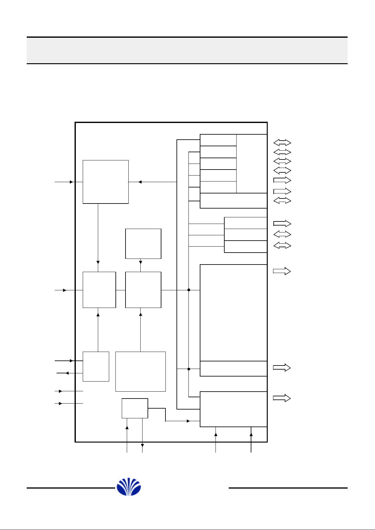
2. DEVICE FUNCTIONS
2.1 Block Diagram
Ext Int
A/D Con
TIMER 1
TIMER 2
TIMER 3
I2C
B PORT
C PORT
D PORT
6-Bit PWM
14-Bit PWM
/RESET
TEST
IN
OUT
VCC
VSS
A PORT
B PORT
Interrupt
Control
On-Screen
Display
RAM
256 Bytes
Peripheral
& Memory
Control
8-Bit
CPU
ROM
16K Bytes
CPU
OSD
OSD
OSC
IN OUT /Hsync /Vsync
A0(ADC)
PWM1_0
PWM1_1
PWM1_2
PWM1_3
PWM1_4
PWM1_5
PWM1_6
PWM1_7
PWM1_8
PWM0
RED
GREEN
BLUE
Yout or /Yout
B0-B7
C0-C7
D0-D3
A1-A2(ECI)
A3-A5(INT)
A6-A7
B0(T1OUT)
B1(T3OUT)
SDA, SCL
£Ä£Á£Å£×£Ï£Ï
DAEWOO ELECTRONICS CO., LTD.
Page 6
6
8Bit Single Chip Microcontroller
DMC73C167
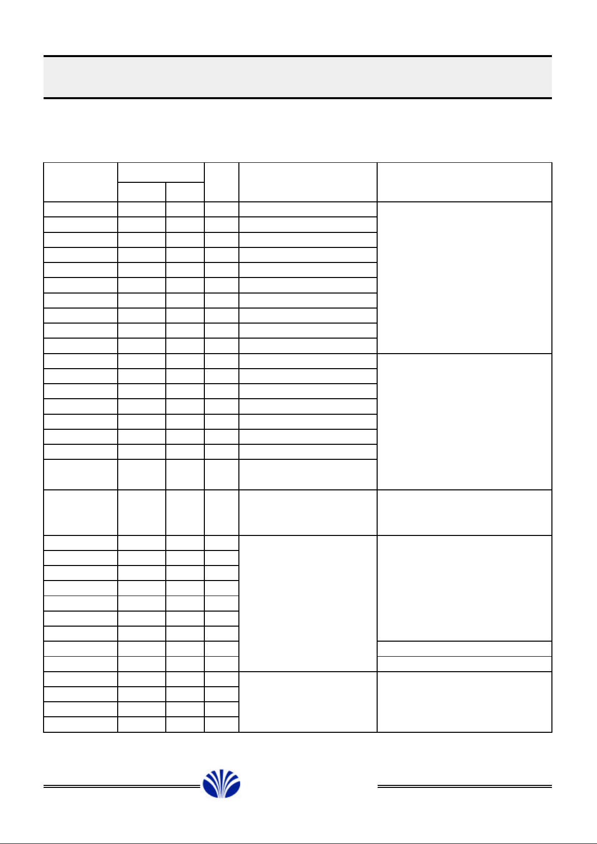
2.2 Pin Description
Pin Pin Number
Symbol Primary SE
PWM0 1 1 O 14-bit PWM output CMOS output
PWM1_0 2 2 O 6-bit PWM output 0 PWM1_0 to PWM1_8
PWM1_1 3 3 O 6-bit PWM output 1 are output pins with
PWM1_2 4 4 O 6-bit PWM output 2 +12V open drain
PWM1_3 5 5 O 6-bit PWM output 3
PWM1_4 6 6 O 6-bit PWM output 4
PWM1_5 7 7 O 6-bit PWM output 5
PWM1_6 8 8 O 6-bit PWM output 6
PWM1_7 9 9 O 6-bit PWM output 7
PWM1_8 10 10 O 6-bit PWM output 8
B0/T1OUT 11 11 O Output, Timer 1 clock out B0 to B3 are optional use
B1/T3OUT 12 12 O Output, Timer 3 clock out for open-drain output
B2 13 13 O Output with +12V buffer
B3 14 14 O Output
B4 15 15 O Output B4 to B7 are optional use
B5 16 16 O Output for open-drain output with
B6 17 17 O Output 12mA drive(+5V) or internal
B7 18 18 O Output pull up(+5V) resistor by mask
option
A0 19 19 I/O ADC input or normal I/O 4-bit A/D converter or normal
I/O internal pull up(+5V)
resistor (mask option)
C0 20 20 I/O Digital I/O C0 to C7 are normal I/O pins
C1 21 21 I/O and internal resistors can be
C2 22 22 I/O optionally pulled up(+5V )
C3 23 23 I/O during masking process
C4 24 24 I/O
C5 25 25 I/O
C6 26 26 I/O
VSS 27 27 I Ground reference
C7 28 38 I/O
D0 29 39 I/O Digital I/O D0 to D3 are normal I/O pins
D1 30 40 I/O and internal resistors can be
D2 31 41 I/O optionally pulled up(+5V)
D3 32 42 I/O during masking process
Function
Description
I/O
£Ä£Á£Å£×£Ï£Ï
DAEWOO ELECTRONICS CO., LTD.
Page 7
7
8Bit Single Chip Microcontroller
DMC73C167
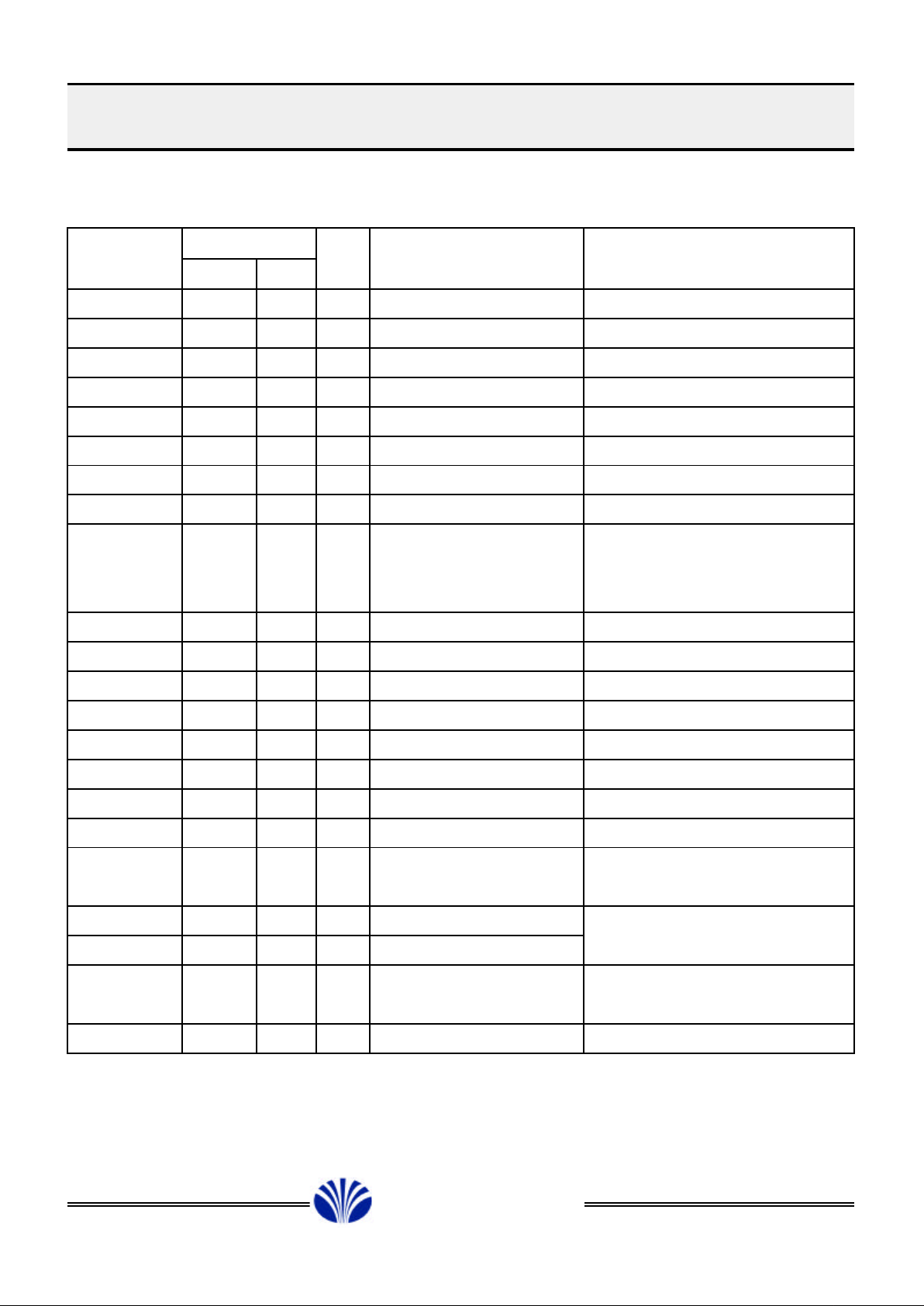
2.2 Pin Description (Continued)
Pin Pin Number
Symbol Primary SE
RED 33 43 O OSD red color output CMOS output
GREEN 34 44 O OSD green color output CMOS output
BLUE 35 45 O OSD blue color output CMOS output
Yout 36 46 O OSD blanking signal Active high or low(mask option)
/HYSNC 37 47 I H SYNC input OSD H position reference
/VSYNC 38 48 I V SYNC input OSD V position reference
OSCI_OSD 39 49 I Clock input for OSD
OSCO_OSD 40 50 O Clock output for OSD
A2(ECI2) 41 51 I/O I/O, Timer 2 clock input Internal pull-up(+5V) resistor
(mask option). Event counter
or normal I/O
TEST 42 52 I Should be fixed to 0 For device test
OSCI_CPU 43 53 I Clock input for CPU
OSCO_CPU 44 54 O Clock output for CPU
/RESET 45 55 I For CPU reset
A1(ECI1) 46 56 I/O I/O, Timer 1 clock input Event counter or normal I/O
A3(INT1) 47 57 I/O External interrupt 1 With Schmitt trigger
A4(INT3_0) 48 58 I/O External interrupt 3_0 With Schmitt trigger
A5(INT5_0) 49 59 I/O External interrupt 5_0 With Schmitt trigger
A6 50 60 I/O Digital I/O A0 to A6 can be optionally pulled
up(+5V) during masking process
SDA 51 61 I/O Data pin for I2C Open drain(+5V) with
SCL 52 62 I/O Clock pin for I2C Schmitt input
A7 53 63 I/O Digital I/O Internal pull-up(+5V) resistor
(mask option)
VCC 54 64 I 4.5V-5.5V
Function
Description
I/O
£Ä£Á£Å£×£Ï£Ï
DAEWOO ELECTRONICS CO., LTD.
Page 8
8
8Bit Single Chip Microcontroller
DMC73C167
3. ELECTRICAL SPECIFICATIONS
3.1 Absolute Maximum Ratings
Parameter Symbol Rating Unit
Supply voltage range* VCC -0.3 through 7.0 V
Input voltage range VI -0.3 through VCC +0.3 V
Output Port B0-B3, PWM1_n -0.3 through 15.0 V
voltage range Except B0-B3, PWM1_n -0.3 through VCC +0.3
Input current II ±10 mA
Output Port B4-B7 IO Max 20 mA
current Except B4-B7 Max 10
Total low-level output current IOL Max 120 mA
Power dissipation PD 0.5 W
Storage temperature range TSTG -55 through +125
¡É
*Unless otherwise noted, all voltages are with respect to VSS.
Test pin must connect to VSS.
Pull-up resistor option is not counted in the electrical specifications.
Stresses beyond those listed under "Absolute Maximum Ratings" may cause permanent
damage to the device. This is a stress rating only and functional operation of the device
at these or any other conditions beyond those indicated in Section " Recommended
Operating Conditions" of this specification is not implied.
Exposure to absolute-maximum-rated conditions for extended periods may affect
device reliability.
£Ä£Á£Å£×£Ï£Ï
DAEWOO ELECTRONICS CO., LTD.
Page 9
9
8Bit Single Chip Microcontroller
DMC73C167
3.2 Recommended Operating Conditions
Parameter Symbol Port Min Typ Max Unit
Supply voltage* VCC 4.5 5.5 V
Operating free-air TOPR
-10¡É 70¡É
Deg
temperature range**
High-level input voltage VIH OSC IN*** VCC-0.7 VCC V
Except OSC IN**** VCC-1.0 VCC V
Low-level input voltage VIL OSC IN*** VSS 0.4 V
Except OSC IN**** VSS 1.1 V
Positive-going threshold VT+ # A3-A5, /RESET 2.5 4.0 V
Negative-going threshold VT- # A3-A5, /RESET 1.0 2.0 V
Hysteresis VH # A3-A5, /RESET, /Hsync, 1.0 V
/Vsync, SCL, SDA
Oepn-drain port supply PORT B0-B3, PWM1_n 4.5 12 14.0 V
voltage PORT B4-B7, SCL, SDA 4.5 5 5.5 V
Analog input voltage A0 VSS VCC V
* Ripple must not exceed 50mVp-p
** See A/D Converter Characteristics
*** OSCIN means both CPU and OSD OSCIN
**** Except Schmitt-trigger inputs
££ VCC = 5.0V
£Ä£Á£Å£×£Ï£Ï
DAEWOO ELECTRONICS CO., LTD.
Page 10
10
8Bit Single Chip Microcontroller
DMC73C167
3.3 Electrical Characteristics
Parameter Symbol Port Min Typ Max Unit
Input current II VI=VSS-VCC ±10.0 mA
High-level output current IOH VOH=VCC-0.5V -0.3 mA
Low-level output current IOL SCL, SDA VOL=0.4V 3 mA
B4-B7 VOL=1.0V 12 16
Except SCL, SDA, B4-B7 1.7
VOL=0.4V
High-level output voltage VOH IOH= -0.3mA VCC-0.5 VCC V
Low-level output voltage VOL IOL=1.7mA 0.4 V
Low-level output B0-B3, PWM1_n VO=12V ±10
leakage current ILEAK Excpet B0-B3, PWM1_n ±10 uA
VO=VCC
Internal pull-up resister II VDD=5.0V VI=VSS -60 -90 -120 uA
option
Clock frequency FOSC CPU clock 3.0 6.0 MHz
OSDCLK OSD clock 4.0 8.0
Input capacitance CI 15.0 pF
Supply current* ICC Operation mode 12.0 20.0 mA
Halt mode 5 20 uA
*All I/O terminals which except CLKIN are open and VCC=5V.
£Ä£Á£Å£×£Ï£Ï
DAEWOO ELECTRONICS CO., LTD.
Page 11
11
8Bit Single Chip Microcontroller
DMC73C167
3.4 AC Characteristics
I/O Port
Parameter Port Conditions Min Typ Max Unit
SCL SDA B0-B7 CL=50pF 1 us
I/O Port output PWM1_n*
rise time Except SCL, SDA, CL=15pF 30 60 ns
B0-B7, PWM1_n CL=50pF 150
SCL SDA B0-B7 CL=50pF 1 us
I/O Port output PWM1_n*
fall time Except SCL, SDA, CL=15pF 10 40 ns
B0-B7, PWM1_n CL=50pF 70
* External pull-up registers are needed in PWM1_n, B0-B3.
External pull-up registers are also needed in SCL, SDA. The values would be recommendable
to fit rise and falling time of I2C spec.
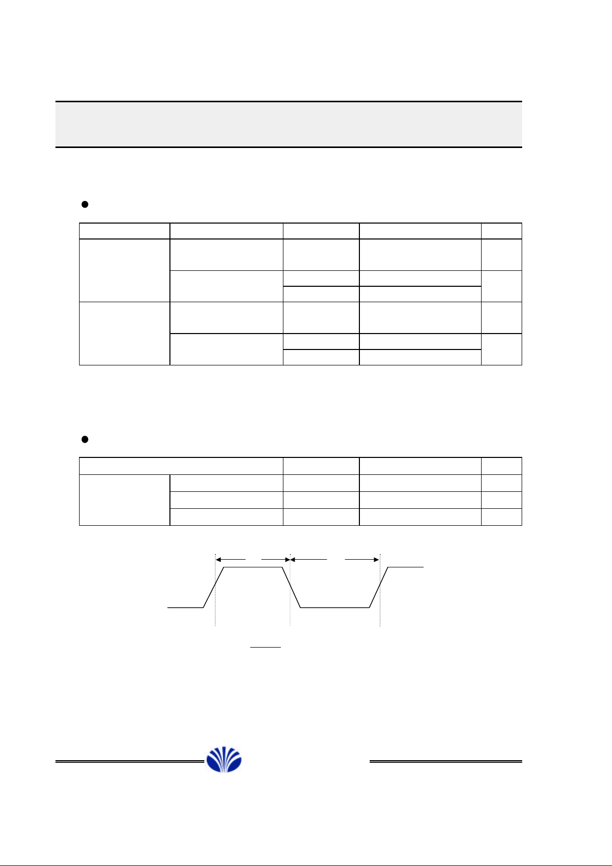
Clock I/O
Parameter Symbol Min Typ Max Unit
Rise time tr(c) 20 ns
Clock pulse Fall time tf(c) 10 ns
Duty cycle dty(c) 45 50 55 %
Note : Timing points are 90%(high) and 10%(low).
- Externally Driven Clock Input Waveform -
£Ä£Á£Å£×£Ï£Ï
DAEWOO ELECTRONICS CO., LTD.
XY
DUTY(%) = Tc(c) = X + Y
Tc(c)
X or Y
x 100
Page 12
12
8Bit Single Chip Microcontroller DMC73C167
3.4 AC Characteristics (Continued)
A/D Converter
Parameter Test Conditions Min Typ Max Unit
Resolution 4 bit
Non-linearity TOPR = -10°through +70°
Zero error VCC = 5V±10% ±1/2 ±1 LSB
Full-scale error VSS = 0V, FOSC = 6MHz
Conversion time* 13.3 uS
* External sample hold circuit is required during 40 machine cycle times. Resolution is dependent
on ripple supply voltage(VCC<VREF). Ripple must not exceed 5mVp-p.
I2C
Parameter Symbol Min Max Unit
SCL clock frequency fSCL 0 100 kHz
Time the bus must be free before
a new transmission can start*
Hold time start condition* tHD;STA 4 us
Low period of the clock* tLOW 4.7 us
High period of the clock* tHIGH 4 us
Setup time for start condition* tSU;STA 4.7** us
Hold time data tHD;DAT 0 us
Setup time data tSU;DAT 250 ns
Rise time of both SDA and SCL lines tR 1 us
Fall time of both SDA and SCL lines tF 300 ns
Setup time for stop condition* tSU;STO 4.7 us
* The value is like above when the digital filter is off. Add 4/Fosc to this value when the
digital filter is on.
** This time must be satisfied by the software delay.
tBUF
4.7
us
£Ä£Á£Å£×£Ï£Ï
DAEWOO ELECTRONICS CO., LTD.
Page 13
13
8Bit Single Chip Microcontroller DMC73C167
3.4 AC Characteristics (Continued)
I2C (Continued)
SDA
SCL
SDA
SCL
- Timing for I2C Bus -
tBUF
tR tF
tHD;STA
tHD;DAT
tHIGH
tSU;DAT
tHD;STA
tSU;STA
tSU;STO
£Ä£Á£Å£×£Ï£Ï
DAEWOO ELECTRONICS CO., LTD.
tLOW
Page 14
14
8Bit Single Chip Microcontroller
DMC73C167
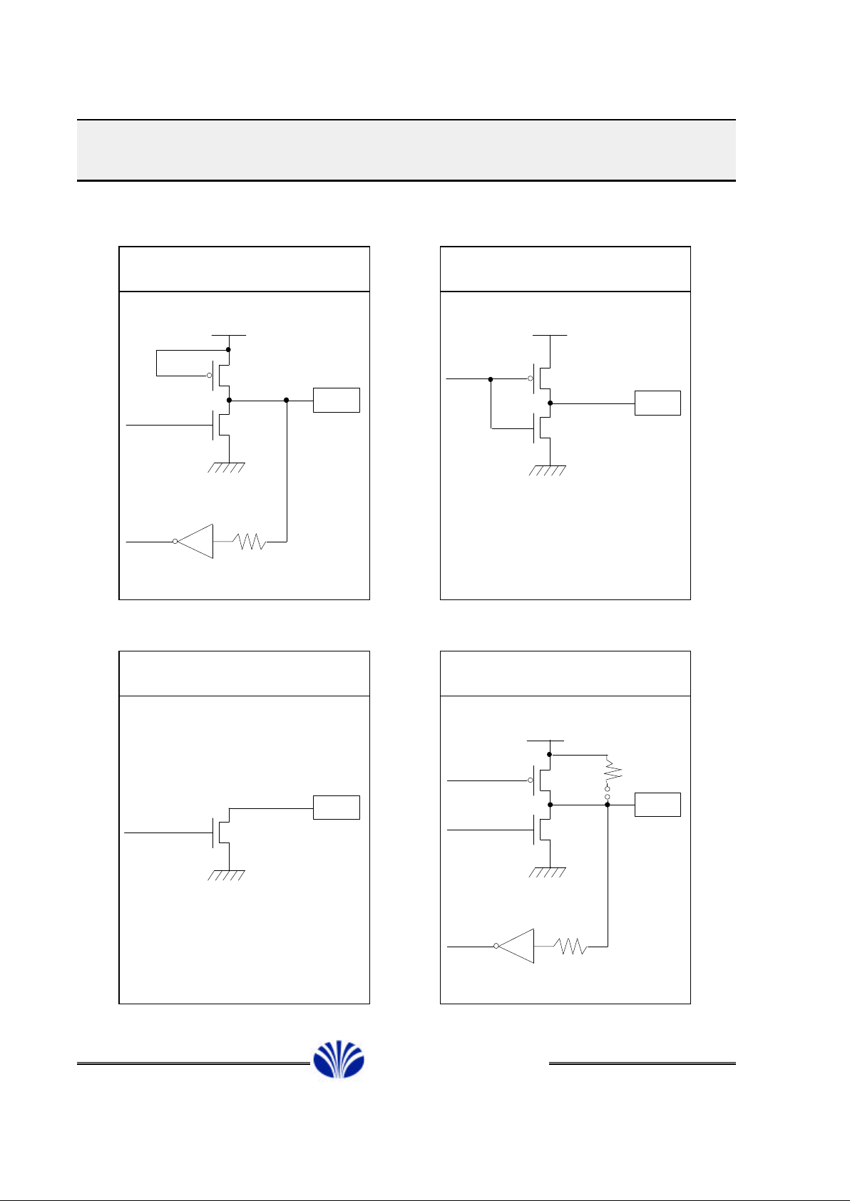
3.5 I / O Circuits
SCL, SDA PWM0, R, G, B, Y
N-CH OPEN DRAIN : 5V CMOS Output
Schmitt Inverter
Port B0-B3, PWM1_0 -PWM1_8 Port A0-A2, A6-A7, C0-C7, D0-D3
N-CH OPEN DRAIN : 12V TEST(SE DEVICE)
(No Inverter on A0 Port)
Vcc
Data Out
Port
Data In
S
Data Out
Port
Data In
Vcc
Data Out
Mask
Option
Vcc
Port
Data Out
Port
Data
Out
£Ä£Á£Å£×£Ï£Ï
DAEWOO ELECTRONICS CO., LTD.
Page 15
15
8Bit Single Chip Microcontroller
DMC73C167
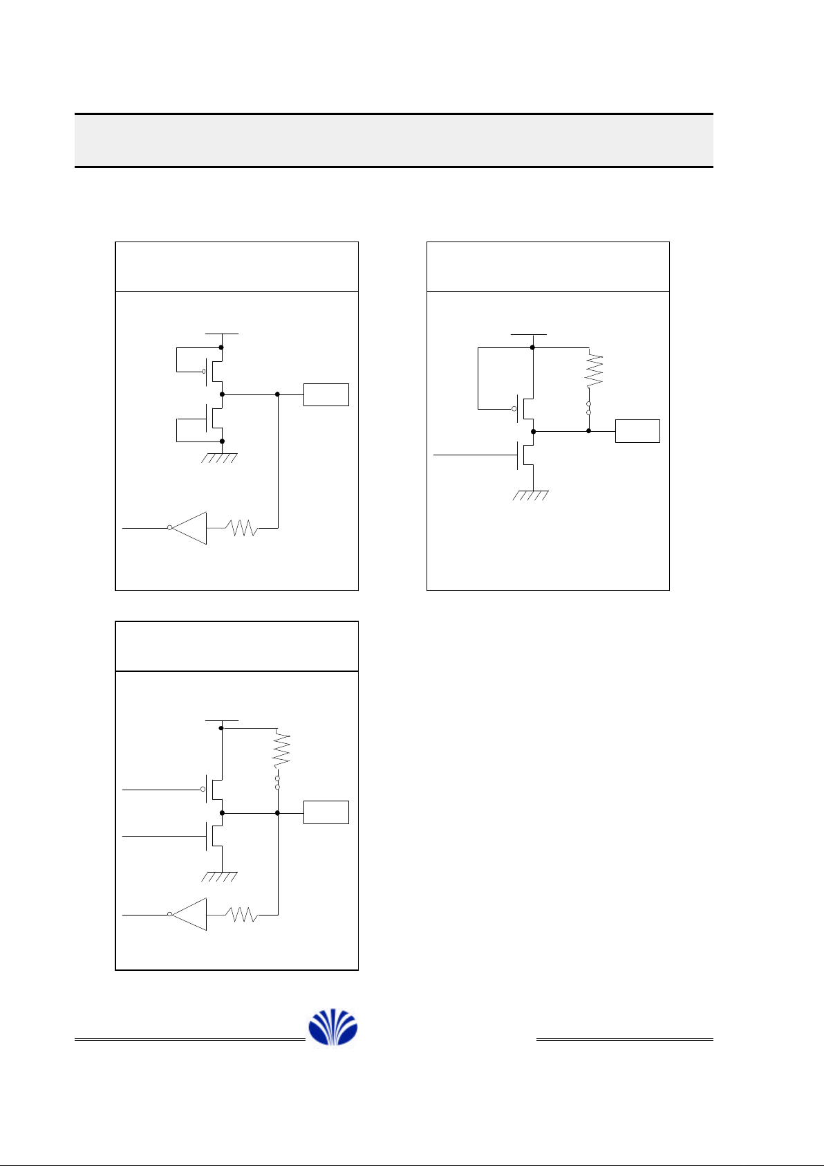
3.5 I / O Circuits (Continued)
/RESET, /Vsync, /Hsync Port B4-B7
TEST(Primary) Input Only OPEN DRAIN : 5V, 12mA
Mask Option
NO : 12mA Current Drive Port
Schmitt Inverter (Except TEST) YES : Internal Pull up
A3, A4, A5
I/O Port
Schmitt Inverter
Vcc
Port
Data In
S
Port
Vcc
Mask
Option
Vcc
Data Out
Port
Data In
S
Mask
Option
Data Out
£Ä£Á£Å£×£Ï£Ï
DAEWOO ELECTRONICS CO., LTD.
Page 16

16
8Bit Single Chip Microcontroller DMC73C167
4. ARCHITECTURE
4.1 Overview
The DMC73C167 has a maximum memory address space of 16 kbytes on-chip ROM and
only a single-chip mode. On-chip memory spaces are configured as shown if Figure 4-1
below. In the section that follow, the register file(RF) and the peripheral file(PF) are described
along with three important registers in the CPU : the stack pointer(SP), the status register
(ST), and the program counter(PC).
Figure 4-1. DMC73C167 Memory Maps
Memory address
0000h
Register File (RF)
00FFh
0100h
Peripheral File (PF)
01FFh
0200h
Not Available
C005h
C006h
16Kbytes ROM
FFFFh
4.2 Register File (RF)
The 256-byte on-chip RAM resides in locations 0000h to 00FFh of the DMC73C167's
address space and is called the register file (RF). The RAM is treated as a register by much
of the instruction set and is numbered R0-R255. The first two registers, R0 and R1, are also
called the A and B registers, respectively. Several instructions specify A or B as either the
source or destination register. For example, STSP stores the contents of the stack pointer
(SP) in the B register. Except where stated otherwise, any register in the register file can be
addressed as an 8-bit source or destination register. The stack is also located in the register
file. Refer to Section 4.4 for information regarding the initialization of the stack pointer and
stack definition in the register file.
£Ä£Á£Å£×£Ï£Ï
DAEWOO ELECTRONICS CO., LTD.
Page 17

17
8Bit Single Chip Microcontroller DMC73C167
4.3 Peripheral File (PF)
The peripheral file (PF) resides in location 0100h to 01FFh of the DMC73C167's
address space. Some of the instructions are optimized for efficient access to and from
the registers that reside in the peripheral file. Peripheral file locations are number P0-P255.
The PF registers are used for interrupt control, parallel I/O, timer control, 14-bit
PWM, OSD, 6-bit PWM, I2C and A/D converter control. On screen Display RAM (video
RAM) is also mapped in the peripheral file.
Figure 4-2. DMC73C167 Peripheral File Map
Memory address
100h
P0
: Peripheral Registers
P75
14Bh
14Ch
P76
: Reserved
P95
15Fh
160h
P96
: Line A Video RAM
P115
173h
174h
P116
: Reserved
P127
17Fh
180h
P128
: Line B Video RAM
P147
193h
194h
P148 Not Available
:
P255
1FFh
£Ä£Á£Å£×£Ï£Ï
DAEWOO ELECTRONICS CO., LTD.
Page 18
18
8Bit Single Chip Microcontroller DMC73C167
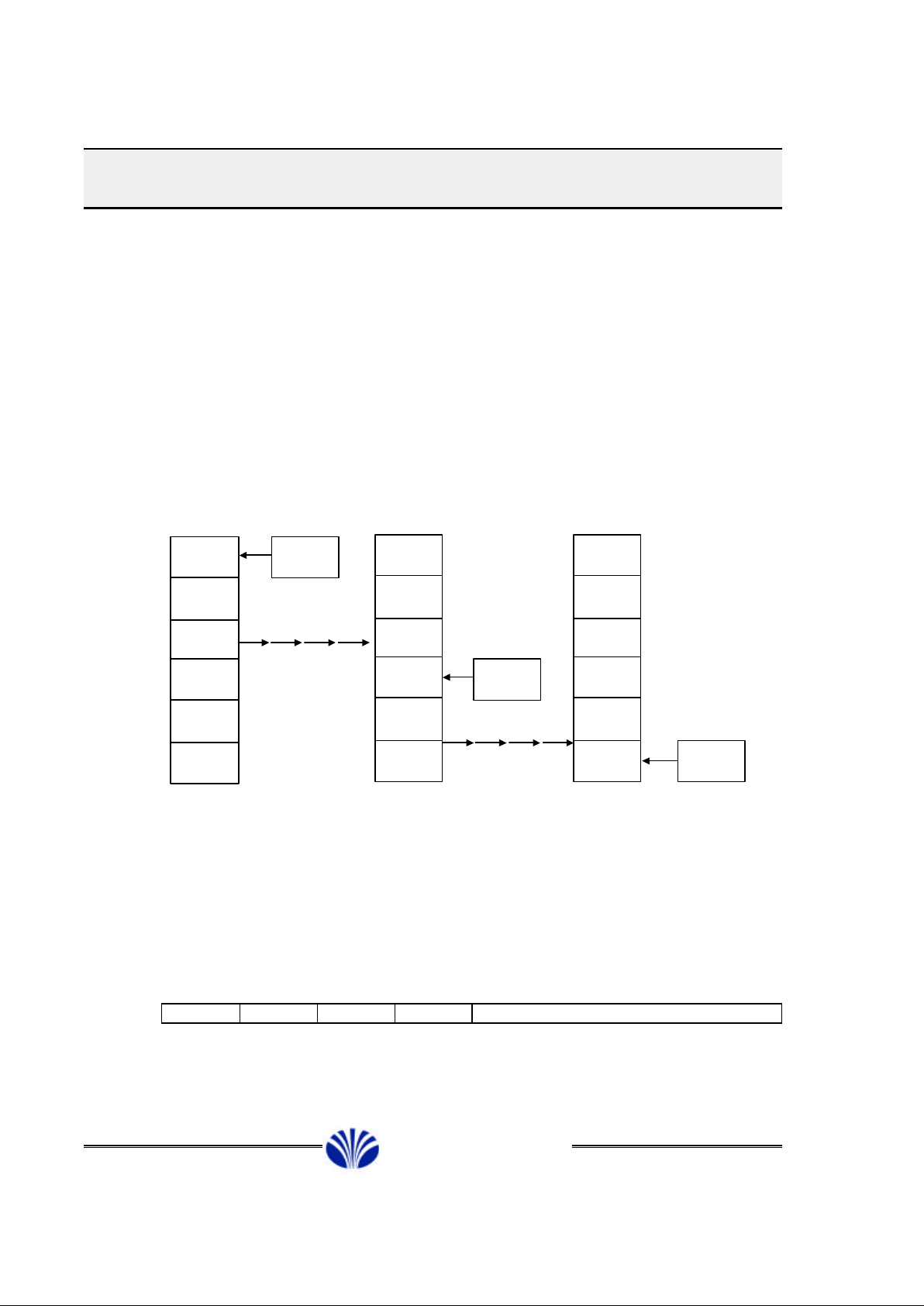
4.4 Stack Pointer (SP)
The stack pointer(SP) is an 8-bit register in the CPU which is typically used to hold a pointer
in RAM (the register file). However, the SP can also be used as temporary data storage if a
stack is not implemented, or if the SP contents are not needed.
When a stack is implemented, the SP points to the last or top entry on the stack. The SP
is automatically incremented just before data is pushed onto the stack and automatically
decremented immediately after data is popped from the stack. Upon assertion of the
RESET function (see Section 4.8) 01h is loaded into the SP. The size of the stack can be
changed from the 255-level stack at RESET to a smaller stack by execuiting a stack
initialization program as illustrated in Figure 4-3. This feature allows the stack to be located
anywhere in the register file. The SP is initialized through the B register (R1).
Figure 4-3. Example of Stack Initialization in the Register File
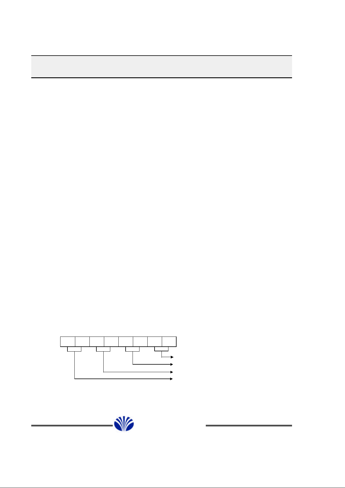
4.5 Status Register (ST)
The status register(ST) is an 8-bit register in the CPU that contains three conditional status
bits : carry(C), sign(N), and zero(Z). It also contains a global interrupt enable bit(I) as shown
in Figure 4-4 below.
Figure 4-4. Status Register (ST)
Bit 7 6 5 4 3 2 1 0
Con C N Z I Future use
C = carry out, N=sign, Z = zero, I = Interrupt enable
0001h
0002h
0003h
0004h
0005h
0006h
01h
ST
PCH
PCL
04h
PCH
PCL 06h
RFSPRF
RFSPCall
£Ä£Á£Å£×£Ï£Ï
DAEWOO ELECTRONICS CO., LTD.
Page 19
19
8Bit Single Chip Microcontroller DMC73C167
The C, N and Z bits are used mostly for arithmetic operations, bit rotating, and conditional
branching. The carry (C) bit is used as the carry-in and the carry-out for most of the rotate
and arithmetic instructions. The sign(N) bit contains the most significant bit of the
desitination operand contents after instruction execution. The zero(Z) bit contains a 1 when
all bits of the destination operand are equal to zero after instruction execution.
The C, N, and Z status bits also have jump-on-condition instructions associated with them.
The global interrupt enable(I) bit must be set to 1 by the EINT instruction in order for any of
the individual interrupts (INTn) to be recognized by the CPU. The interrupt enable(I) bit can
be cleared by the DINT instruction or by execuiting a device RESET (see Section 4.8).
4.6 Program Counter (PC)
The DMC73C167's 16-bit program counter (PC) consists of two 8-bit registers in the
CPU which contain the MSB and the LSB, respectively, of a 16-bit address , the program
counter high (PCH) and program counter low (PCL). The PC acts as the 16-bit address
pointer of the opcodes and operands in the memory of the currently executing instruction.
Upon assertion of the RESET function, the MSB and the LSB of the PC are loaded into the
A and B registers of the register file (see Section 4.8).
4.7 Peripheral File Map
The peripheral file(PF) resides in location 0100h through 01FFh of the DMC73C167's
address space, as shown in Tables 4-2.
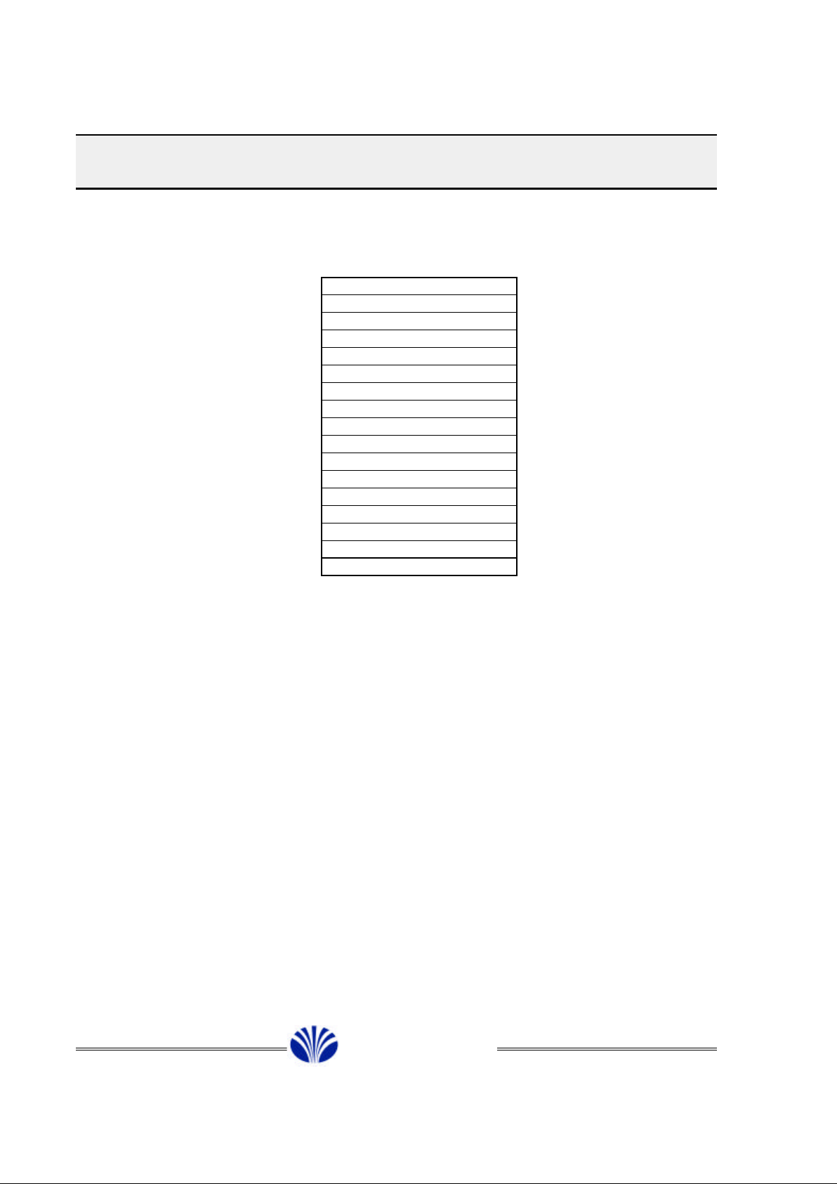
Note : The right-end column, headed "Value After Reset", indicates a reset initial value as
shown in Table 4-1.
Table 4-1. Description of "Value After Reset"
MSB LSB
7 6 5 4 3 2 1 0
- - X X O O 1 1
Becomes value "1" after RESET
Becomes value "0" after RESET
Unkown value after RESET
Not Used
£Ä£Á£Å£×£Ï£Ï
DAEWOO ELECTRONICS CO., LTD.
Page 20

20
8Bit Single Chip Microcontroller DMC73C167
Table 4-2. Peripheral File Map
Value after Reset
MSB LSB
Number Address Label R/W Contents 5
P0 0100h IOCTL0 R/W Interrupt control 0
P1 0101h IOCTL1 R/W Interrupt control 1 - - - P2 0102h IOCTL2 R/W Interrupt control 2 - - - - P3 0103h IOCTL3 R/W Interrupt control 3 0
P4 0104h IOCTL4 R/W Interrupt control 4 - - 0
P5 0105h - - Reserved
P6 0106h ADATA R A Port data X X X XXXXX
P7 0107h ADIR R/W A Port direction register 0
P8 0108h BDATA R/W B Port data 1
P9 0109h - - Reserved
P10 010Ah CDATA R/W C Port data XX X XX X XX
P11 010Bh CDIR R/W C Port direction 0
P12 010Ch DDATA R/W D Port data - - - - XXX X
P13 010Dh DDIR R/W D Port direction - - - P14 010Eh - - Reserved
P15 010Fh - - Reserved
P16 0110h ADCTL R/W A/D control - 0
P17 0111h ADDATA R A/D data - - - P18 0112h - - Reserved
P19 0113h - - Reserved
P20 0114h T1MSD R/W Timer 1 MS data XX X X XX X X
P21 0115h T1LSD R/W Timer 1 LS data X X X X XX X X
P22 0116h T1CTL0 R/W Timer 1 control X XX X XX
P23 0116h T1CTL1 R Timer 1 control 1 X X XX X XX
P24 0117h T2DATA R/W Timer 2 data XX X X XX X X
P25 0119h T2CTL R/W Timer 2 control X X X XX X
P26 011Ah T3DATA R/W Timer 3 data XX X X XX X X
P27 011Bh T3CTL R/W Timer 3 control - - - - XX
P28 011Ch - - Reserved
P29 011Dh - - Reserved
P30 011Eh - - Reserved
P31 011Fh - - Reserved
P32 0120h PWM0CTL R/W 14-bit PWM control - - - - P33 0121h WAKEMS R/W Wake up MS counter - - 0
P34 0122h WAKELS R/W Wake up LS counter 0
P35 0123h PWM0AT W 14-bit PWM add time - - 0
P36 0124h PWM0BT W 14-bit PWM base time 0
P37 0125h PWM1CTL R/W 6-bit PWM control - - - - - - P38 0126h PWM1_0T W PWM1_0 polarity and time - 0
P39 0127h PWM1_1T W PWM1_1 polarity and time - 0
P40 0128h PWM1_2T W PWM1_2 polarity and time - 0
£Ä£Á£Å£×£Ï£Ï
DAEWOO ELECTRONICS CO., LTD.
Page 21

21
8Bit Single Chip Microcontroller DMC73C167
Table 4-2. Peripheral File Map (Continued)
Value after Reset
MSB LSB
Number Address Label R/W Contents 5
P41 0129h PWM1_3T W PWM1_3 polarity and time - 0
P42 012Ah PWM1_4T W PWM1_4 polarity and time - 0
P43 012Bh PWM1_5T W PWM1_5 polarity and time - 0
P44 012Ch PWM1_6T W PWM1_6 polarity and time - 0
P45 012Dh PWM1_7T W PWM1_7 polarity and time - 0
P46 012Eh PWM1_8T W PWM1_8 polarity and time - 0
P47 012Fh - - Reserved
P48 0130h MCTL0 R/W I2C master control 0 - 0
P49 0131h MCTL1 R/W I2C master control 1 - - - P50 0132h MSTS R/W I2C master status 0 - - - P51 0133h MDATA R/W I2C master data X X X XX X XX
P52 0134h HDC R/W I2C master high duration X X X X XX X X
P53 0135h LDC R/W I2C master low duration XX X XX X XX
P54 0136h SADDR W I2C slave address XX X X X XX X
P55 0137h SDATA R/W I2C slave data X X X XX X XX
P56 0138h SCTL R/W I2C slave control - - P57 0139h DFCTL R/W I2C digital filter control - - - - - P58-P67 013Ah-0143h - - Reserved for on-chip PF
P68 0144h OSDCTL R/W OSD control register - - P69 0145h OSDHP W OSD horizontal position - 1
P70 0146h OSDVPA W LINE A vertical position 1
P71 0147h OSDVPB W LINE B vertical position 1
P72 0148h VPCNTR R Vertical display counter - - - P73-P75 0149h-014Bh - - Reserved
P77-P95 0150h-015Fh - - Reserved for on-chip PF
P96-P115 0160h-0173h - W OSD LINE A video RAM XX X X XX X X
P128-P147
0180h-0193h - W OSD LINE B video RAM XX X X X XX X
P148-P255
0194h-01FFh - - Not available
£Ä£Á£Å£×£Ï£Ï
DAEWOO ELECTRONICS CO., LTD.
Page 22

22
8Bit Single Chip Microcontroller DMC73C167
4.8 Interrupt and Reset Priorities
The DMC73C167 has priority servicing of five interrupt levels and RESET. These levels
are defined as shown in Table 4-3. The TRAP instructions branch to two-byte location in a
reserved section of memory called the TRAP vector table. As shown in Figure 4-5. each trap
location stores a 16-bit address that references either the reset function (TRAP0), one of the
five interrupt service routines (TRAP1-INT1, TRAP2-INT2, TRAP3-INT3, TRAP4-INT4, TRAP5INT5), or a subroutine (TRAP6-23). Once the interrupt has been acknowledged, the CPU then
pushes the contents of the status register and the program counter (MSB and LSB) onto the
stack and zeros the status register, including the global interrupt Enable (I) bit.
The CPU reads an interrupt code from the interrupt logic and branches to the address
contained in the corresponding interrupt vector location in memory. The interrupt service routine
can explicitly enable nested interrupts by executing the EINT instruction to directly set the I bit
in the status register to 1, thus permitting routine is completed, it returns to the previous interrupt
service routine by executing the RETI instruction.
Table 4-3. Interrupt and Reset Priorities
Level Name Source Trigger Factor Vector
MSB LSB
0 /Reset External Active Low FFFEh FFFFh
1 INT1 External Falling/Rising FFFCh FFFDh
2 INT2_0 Timer 1 Timer 1 underflow FFFAh FFFBh
INT2_1 Timer 2 Timer 2 underflow
3 INT3_0 External Falling/Rising FFF8h FFF9h
INT3_1 Timer 3 Timer3 underflow
4 INT4 OSD OSD enable FFF6h FFF7h
5 INT5_0 External Falling/Rising FFF4h FFF5h
INT5_1 12C master Data ready from slave
INT5_2 12C slave Slace address selected
£Ä£Á£Å£×£Ï£Ï
DAEWOO ELECTRONICS CO., LTD.
Page 23
23
8Bit Single Chip Microcontroller DMC73C167
Figure 4-5. TRAP Vector Table
Address
FFD0h TRAP23 (MSB) *
FFD1h TRAP23 (LSB) **
/ ////////
FFEFh TRAP8 (A0-A7)
FFF0h TRAP7 (MSB)
FFF1h TRAP7 (LSB)
FFF2h TRAP6 (MSB)
FFF5h INT5 or TRAP5 (LSB)
FFF7h INT4 or TRAP4 (LSB)
FFF8h INT3 or TRAP3 (MSB)
FFF9h INT3 or TRAP3 (LSB)
FFFAh INT2 or TRAP2 (MSB)
FFFBh INT2 or TRAP2 (LSB)
FFFCh INT1 or TRAP1 (MSB)
FFFDh INT1 or TRAP1 (LSB)
FFFEh RESET or TRAP0 (MSB)
FFFFh RESET or TRAP0 (LSB)
* MSB = A8-A15
** LSB = A0-A7
£Ä£Á£Å£×£Ï£Ï
DAEWOO ELECTRONICS CO., LTD.
Page 24

24
8Bit Single Chip Microcontroller DMC73C167
5. FUNCTION
5.1 Input/Output Ports
The DMC73C167 has 28 I/O pins organized as four parallel ports labeled
A, B, C and D. Each port is mapped into 4- to 8-bit data value resiters in the peripheral file (PF).
The data value registers are usually called APORT, BPORT, CPORT and DPORT in a program.
Ports A, C and D are implemented as bidirectional I/O ports.
Port B is an open-drain output only port with a 12 V buffer (B0-B3)and 12mA current drive
capability (B4-B7).
Each bidirectional port (that is, Port A, C and D) has a corresponding data direction register
(DDR) that programs each I/O pin as an input or output pin. A bit set to 1 in the DDR will
cause the corresponding pin to be an output pin, while a 0 in the DDR will turn the pin into
a high-impedance input pin. Upon RESET, the DDR filp-flop registers are set to 0 by the
on-chip circuitry, forcing them to become inputs. Also upon RESET, the output data registers
of the output only port (that is, Port B) are set to 1 by the on-chip circuitry. And, other output
data registers are indeterminated data set.
After RESET, if 1s are writtern to the DDR register sometime before the output data register
is changed, then the corresponding I/O pins will output a 1. For this reason, it is good
practice to load the output data registers of Ports A, C and D with the desired value before
any bits are configured as outputs. In addition, DMC73C167 has several mask options
related to the I/O pins such as pull-up resistors. Those I/O pins are individually configurable
at the masking stage. For a detailed description of the I/O pins in the DMC73C167,
see table 3-2.
5.1.1 A Port
Pins A0 to A7 of A port are bidirectional I/O ports and several hardware-related functions are
interfaced with the CPU through this port. Pin A0 can be used as an analog input for the onchip A/D converter. Pin A1 and A2 can be used for the event counter input of Timer 1 and
Timer 2, respectively. Pin A3, A4 and A5 can be used for the Schmitt-buffered external interrupt
input for INT1, INT3_0, and INT5_0, respectively.
Reading the port - A data register (P6) returns each value at the A0 - A7 pins if the
corresponding DDR bit is set to 0 and returns each output buffer register value if the DDR
bit is 1. The user can specify internal pull-up (5V) resistor insertion or not selectively for port
A pins (mask option).
Table 5-1. P7 0107h ADDR A Port Direction
Bit 7 6 5 4 3 2 1 0
R
W
ADDR7 ADDR6 ADDR5 ADDR4 ADDR3 ADDR2 ADDR1 ADDR0
£Ä£Á£Å£×£Ï£Ï
DAEWOO ELECTRONICS CO., LTD.
Page 25
25
8Bit Single Chip Microcontroller DMC73C167
Table 5-2. P6 0106h ADATA A Port Data
Bit 7 6 5 4 3 2 1 0
R
W
ADATA7 ADATA6 ADATA5 ADATA4 ADATA3 ADATA2 ADATA1 ADATA0
Special - - INT5_0 INT3_0 INT1 ECI2 ECI1 ADIN
Table 5-3. A Port Control Register Operation
ADDRn Driection ADATAn(Read) ADATAn(Write)
0 Input Port 0 ; Input 'Low' Invalid
1 : Input 'High'
1 Output Port Written Data 0 ; Output 'Low'
1 : Output 'High'
Note :
Special usage for Pin A0 to A5 is as follows.
ADIN : Analog signal for 4-bit ADC is acceptable through Pin A0. Bit 0 for the A/D
control register (ADCTL, P16) controls digital input or analog input.
To use analog input, pin A0 must be in input mode (ADDR0-0).
ECI1 : Event counter input for Timer 1
The external clock from Pin A1 can be directly connected to the clock source of
Timer 1. T1SRC (bit 5 of P22) selects the source of Timer 1.
See Timer 1 operation for more details.
ECI2 : Event counter input for Timer 2.
The external clock from Pin A2 can be directly connected to the clock source of
Timer 2. T2SRC (bit 5 of P25) selects the source of Timer 2.
See Timer 2 operation for more details.
INT1 : External interrupt 1 is triggered by the falling and rising transition of Pin A3,
which must be in input mode to be used as an interrupt source. This pin
can also be used as a normal input port while the interrupt is activated.
INT3_0 : External interrupt 3_0 is triggered by the falling and rising transition of
Pin A4, which must be in input mode to be used as an interrupt source.
This pin can also be used as a normal input port while the interrupt is
activated.
£Ä£Á£Å£×£Ï£Ï
DAEWOO ELECTRONICS CO., LTD.
Page 26
26
8Bit Single Chip Microcontroller DMC73C167
INT5_0 : External interrupt 5_0 is triggered by the falling and rising transition of
Pin A5, which must be the input mode to be used as an interrupt source.
This pin can also be used as a normal input port while the interrupt is
activated.
5.1.2 B Port
Pins B0 to B7 of B Port are output only pins. Pins B0 to B3 contain a high-voltage buffer (12V
nominal) with open-drain output and Pins B4 to B7 contain a high-current output buffer (12mA
nominal). Pins B0 and B1 can be used as the clock output of Timer 1 and Timer 3,
respectively. in the DMC73C167, the user can specify the internal pull-up (5V) resistor
for the B4 to B7 ports selectively (mask option).
Table 5-4. P8 0108h BDATA B Port Data
Bit 7 6 5 4 3 2 1 0
R
W
BDATA7 BDATA6 BDATA5 BDATA4 BDATA3 BDATA2 BDATA1 BDATA0
Special - - - - - - T3OUT T1OUT
The B Port control register operation is as follows.
WRITE : Setting the BDATAn bit to 1 outputs logic high status to the same pin
number and setting BDATAn bit to 0 outputs logic low status to the
same pin number.
READ : External pins are not accessed through the read operation. The CPU
can read data from B Port but it is the contents of the output buffer
register written by the CPU previously.
Note : Special usage for Pins B0 and B1 is as follows.
T1OUT : Clock output for Timer 1
Underflow of Timer 1 MSB decrement register toggles the logic level of Pin B0
When bit 6 of T1CTL0 (P22) is set to 1.
T3OUT : Clock output for Timer 3
Underflow of Timer 3 decrement register toggles the logic level of Pin B1 when
bit 6 of T2CTL (P25) is set to 1.
£Ä£Á£Å£×£Ï£Ï
DAEWOO ELECTRONICS CO., LTD.
Page 27
27
8Bit Single Chip Microcontroller DMC73C167
5.1.3 C Port
The C Port is an 8-bit bidirectional I/O port any of those eight pins can be individually
programmed as input and output lines under software control. In the DMC73C167,
the user can specify internal pull-up (5V) resistor insertion or not selectively for port C
pins (mask option)
Table 5-5. P11 0108h CDDR C Port Direction
Bit 7 6 5 4 3 2 1 0
R
W
CDDR7 CDDR6 CDDR5 CDDR4 CDDR3 CDDR2 CDDR1 CDDR0
Table 5-6. P10 010Ah CDATA C Port Data
Bit 7 6 5 4 3 2 1 0
R
W
CDATA7 CDATA6 CDATA5 CDATA4 CDATA3 CDATA2 CDATA1 CDATA0
Table 5-7. C Port Control Register Operation
CDDRn Driection CDATAn(Read) CDATAn(Write)
0 Input Port 0 ; Input 'Low' Invalid
1 : Input 'High'
1 Output Port Written Data 0 ; Output 'Low'
1 : Output 'High'
5.1.4 D Port
The D Port is a 4-bit bidirectional I/O port any of those four pins can be individually
programmed as input and output lines under software control. In the DMC73C167, the
user can specify internal pull-up (5V) resistor insertion or not selectively for port D pins
(mask option).
Table 5-8. P13 010Dh DDDR D Port Direction
Bit 7 6 5 4 3 2 1 0
R
W
- - - - DDDR3 DDDR2 DDDR1 DDDR0
£Ä£Á£Å£×£Ï£Ï
DAEWOO ELECTRONICS CO., LTD.
Page 28

28
8Bit Single Chip Microcontroller DMC73C167
Table 5-9. P12 010Ch DDATA D Port Data
Bit 7 6 5 4 3 2 1 0
R
W
- - - - DDATA3 DDATA2 DDATA1 DDATA0
Table 5-10. D Port Control Register Operation
DDDRn Driection DDATAn(Read) DDATAn(Write)
0 Input Port 0 ; Input 'Low' Invalid
1 : Input 'High'
1 Output Port Written Data 0 ; Output 'Low'
1 : Output 'High'
5.2 Device Initialization
Interrupt level 0 (RESET) cannot be masked and will be recognized immediately, even in the
middle of an instruction. To execute the level-0 interrupt, the RESET pin must be held low
for a minimum of five internal clock cycles to guarantee recognition by the device. During
assertion of the RESET pin, the following operations are performed prior to the first
instruction acquisition.
1) All zeros are written to the status register. This disables all interrupts and clears all interrupt
flags.
2) The initialized data is written to the peripheral register.
3) The MSB and LSB values of the program counter just before RESET are stored in the R0
and R1 (A and B) registers, respectively.
4) The stack pointer is initialized to 01h.
5) The MSB and LSB of the reset vector are fetched from locations FFFEh and FFFFh,
respectively (see Table 4-5), and located into the program counter.
5.3 I/O Control Registers
The I/O control registers are lcated in the peripheral file and are responsible for interrupt
control. The DMC73C167 contains the I/O Control 0 (IOCTL0), I/O Control 1 (IOCTL1),
I/O Control 2 (IOCTL2), I/O Control 3 (IOCTL3), and I/O Control 4 (IOCTL4) registers, the
I/O Control registers are mapped into lcations P0 (IOCTL0), P1 (IOCTL1), P2 (IOCTL2), P3
£Ä£Á£Å£×£Ï£Ï
DAEWOO ELECTRONICS CO., LTD.
Page 29

29
8Bit Single Chip Microcontroller DMC73C167
(IOCTL3), and P4 (IOCTL4) of the peripheral file. The individual interrupt mask and resets
are controlled through these registers. The interrupt sources may also be individually
tested by reading the interrupt flags or corresponding input ports. The INTn FLAG values
are independent of the INTn ENABLE values. Writing a 1 to the INTn CLEAR bit will clear
the corresponding INTn FLAG, but writing 0 to the INTn CLEAR bit has no effect on the bit.
For INTn to be recognized by the CPU, three conditions must be met.
1) A 1 must be written to the INTn ENABLE bit in the IOCTL0, IOCTL1, IOCTL3, or IOCTL4
register.
2) The global INTERRUPT ENABLE bit, that is bit 4 in the status register, must be set to 1
by the EINT instruction.
3) INTn must be the highest priority interrupt asserted within an instruction boundary.
Table 5-11. Interrupt Control Registers
P0 0100h IOCTL0 Interrupt Control 0
Bit 7 6 5 4 3 2 1 0
R 0 0 INT3F INT3E INT2F INT2E INT1F INT1E
W INT1CLR
P0 0101h IOCTL1 Interrupt Control 1
Bit 7 6 5 4 3 2 1 0
R Not used INT5F INT5E INT4F INT4E
W INT4CLR
P0 0102h IOCTL2 Interrupt Control 2
Bit 7 6 5 4 3 2 1 0
R Not used INT3_0 INT1 INT5_0
W EDGE EDGE EDGE
P0 0103h IOCTL3 Interrupt Control 3
Bit 7 6 5 4 3 2 1 0
R INT3_1F INT3_1E INT3_0F INT3_0E INT2_1F INT2_1E INT2_0F INT2_0E
W INT3_1C INT3_0C INT2_1C INT2_0C
£Ä£Á£Å£×£Ï£Ï
DAEWOO ELECTRONICS CO., LTD.
Page 30

30
8Bit Single Chip Microcontroller DMC73C167
P0 0104h IOCTL4 Interrupt Control 4
Bit 7 6 5 4 3 2 1 0
R Not used INT5_2F INT5_2E INT5_1F INT5_1E INT5_0F INT5_0E
W - - INT5_0C
Notes :
Different names are labeled for those bits which have a different read/write operation
at the same bit position in the peripheral registers.
Table 5-12. P0 0100h IOCTL0 Interrupt control 0
Bit 7 6 5 4 3 2 1 0
R 0 0 INT3F INT3E INT2F INT2E INT1F INT1E
W INT1CLR
INT3 GLOBAL INT2 GLOBAL EXTERNAL INT1
Bit 0 INT1E. External Interrupt 1 Enable.
0 = INT1 disabled
1 = INT1 enabled
Bit 1 INT1F. External Interrupt 1 Flag.
0 = INT1 not requested.
1 = INT1 pending
Bit 2 INT2E. Interrupt 2 Enable
Enables and disables INT2_0 (Timer 1) and INT2_1 (Timer 2)
0 = Disables INT2.
1 = Enables INT2.
Bit 3 INT2F Interrupt 2 Flag
Any INT2_0 or INT2_1 interrupt request sets this bit to 1. To clear this bit,
write 1 to INT2_0C or INT2_1C of IOCTL3 register, the corresponding bit
of interrupt requested.
0 = INT2_0 and INT2_1 are not requested.
1 = INT2_0 or INT2_1 is pending
Bit 4 INT3E. Interrupt 3 Enable
Enables and disables INT3_0 (External) and INT3_1 (Timer 3)
0 = Disables INT3.
1 = Enables INT3.
Bit 5 INT3F. Interrupt 3 Flag
Any INT3_0 or INT3_1 interrupt request sets this bit to 1. To clear this bit,
write 1 to INT3_0C or INT3_1C of IOCTL3 register, the corresponding bit
£Ä£Á£Å£×£Ï£Ï
DAEWOO ELECTRONICS CO., LTD.
Page 31

31
8Bit Single Chip Microcontroller DMC73C167
of interrupt requested.
0 = INT3_0 and INT3_1 are not requested.
1 = INT3_0 or INT3_1 is pending
Bit 6 Should always be 0.
Bit 7 Should always be 0.
Table 5-13. P1 0101h IOCTL1 Interrupt Control 1
Bit 7 6 5 4 3 2 1 0
R Not used INT5F INT5E INT4F INT4E
W INT4CLR
INT5 GLOBAL OSD
Bit 0 INT4E. OSD Interrupt (INT4) Enable.
0 = Disables OSD interrupt
1 = Enables OSD interrupt
Bit 1 INT4F. OSD Interrupt (INT4) Flag
0 = INT4 is not requested.
1 = INT4 is pending
INT4CLR. Clear OSD Interrupt (INT4) Flag
0= No effect
1 = Clears OSD interrupt INT4 flag
Bit 2 INT5E. Interrupt 5 Enable
This bit enables INT5_0, INT5_1, and INT5_2 interrupt requests.
0 = Disables Interrupt 5
1 = Enables Interrupt 5
Bit 3 INT5F. Interrupt5 Flag
Any interrupt request of INT5_0, INT5_1, or INT5_2 sets this bit to 1.
0 = INT5_0 and INT5_1 are not requested
1 = INT5_0 or INT5_1 is pending
Bit 4-7 Not used in this device.
Table 5-14. P2 0102h IOCTL2 Interrupt Control 2
Bit 7 6 5 4 3 2 1 0
R Not used INT3_0 INT1 INT5_0
W EDGE EDGE EDGE
Bit 0 INT5_0 EDGE. External Interrupt INT5_0 Edge Selection.
0 = INT5_0 interrupt is triggered at falling edge.
1 = INT5_0 interrupt is triggered at rising edge.
£Ä£Á£Å£×£Ï£Ï
DAEWOO ELECTRONICS CO., LTD.
Page 32

32
8Bit Single Chip Microcontroller DMC73C167
Bit 1 INT1 EDGE. External Interrupt INT1 Edge Selection.
0 = INT1 interrupt is triggered at falling edge.
1 = INT1 interrupt is triggered at rising edge.
Bit 2 INT3_0 EDGE. External Interrupt INT3_0 Edge Selection.
0 = INT3_0 interrupt is triggered at falling edge.
1 = INT3_0 interrupt is triggered at rising edge.
Bit 3-7 Not used in this device
Table 5-15. P3 0103h IOCTL3 Interrupt Control 3
Bit 7 6 5 4 3 2 1 0
R INT3_1F INT3_1E INT3_0F INT3_0E INT2_1F INT2_1E INT2_0F INT2_0E
W INT3_1C INT3_0C INT2_1C INT2_0C
TIMER 3 EXTERNAL INT3_0 TIMER 2 TIMER 1
Bit 0 INT2_0E. Timer 1 (INT2_0) Interrupt Enable
0 = Disables Timer 1 (INT2_0) interrupt
1 = Enable Timer 1 (INT2_0) interrupt
Bit 1 INT2_0F. Timer (INT2_0) Interrupt Flag
This flag sets the INT2F bit of IOCTL0 register and requests to jump to the
INT2 interrupt service routine.
0 = Timer (INT2_0) interrupt is not requested.
1 = Timer (INT2_0) interrupt is pending
INT2_0C. Clear Timer 1 (INT2_0) Interrupt Flag.
0 = No effect.
1 = Clear Timer 1 (INT2_0) interrupt flag
Bit 2 INT2_1E. Timer 2( INT2_0) Interrupt Enable
0 = Disables Timer 2 (INT2_1) interrupt
1 = Enable Timer 2 (INT2_1) interrupt
Bit 3 INT2_1F. Timer 2 (INT2-1) Interrupt Flag
This flag sets the INT2F bit of IOCTL0 register and requests to jump to the
INT2 interrupt service routine.
0 = Timer (INT2_1) interrupt is not requested.
1 = Timer (INT2_1) interrupt is pending
INT2_1C. Clear Timer 2 (INT2_1) Interrupt Flag.
0 = No effect.
1 = Clear Timer 2 (INT2_1) interrupt flag
Bit 4 INT3_0E. External Interrupt INT3_0 Enable
0 = Disables INT3_0 interrupt
1 = Enable INT3_0 interrupt
£Ä£Á£Å£×£Ï£Ï
DAEWOO ELECTRONICS CO., LTD.
Page 33

33
8Bit Single Chip Microcontroller DMC73C167
Bit 5 INT3_0F. External Interrupt INT3_0 Flag.
This flag sets the INT3F bit of IOCTL0 register and requests to jump to the
INT3 interrupt service routine.
0 = INT3_0 interrupt is not requested.
1 = INT3_0 interrupt is pending
INT3_0C. Clear INT3_0 Interrupt Flag.
0 = No effect.
1 = Clear INT3_0 interrupt flag
Bit 6 INT3_1F Timer 3 (INT3-1) Interrupt Enable.
0 = Disables Timer 3 (INT3_1) interrupt
1 = Enable Timer 3 (INT3_1) interrupt
Bit 7 INT3_1F. External Interrupt INT3_1 Flag.
This flag sets the INT3F bit of IOCTL0 register and requests to jump to the
INT3 interrupt service routine.
0 = Timer 3 (INT3_1) interrupt is not requested.
1 = Timer 3 (INT3_1) interrupt is pending
INT3_1C. Clear Timer 3 (INT3_1) Interrupt Flag.
0 = No effect.
1 = Clear Timer 3 (INT3_1) interrupt flag
Table 5-16. P4 0104h Interrupt Control 4
Bit 7 6 5 4 3 2 1 0
R Not used INT5_2F INT5_2E INT5_1F INT5_1E INT5_0F INT5_0E
W - - INT5_0C
I2C SLAVE I2C MASTER EXTERNAL INT
Bit 0 INT5_0E. External Interrupt 5_0 Enable
0 = Disables INT5_0 interrupt
1 = Enable INT5_0 interrupt
Bit 1 INT5_0F. External Interrupt 5_0 Flag
This flag sets the INT5F bit of IOCTL1 register and requests to jump to the
INT5 interrupt service routine.
0 = INT5_0 interrupt is not requested.
1 = INT5_0 interrupt is pending
INT5_0C. Clear Interrupt 5_0 Flag
0 = No effect.
1 = Clear INT5_0 interrupt flag
Bit 2 INT5_1E. I2C MASTER Interrupt 5_1 Flag
0 = Disables I2C MASTER INT5_1 interrupt
1 = Enable I2C MASTER INT5_1 interrupt
£Ä£Á£Å£×£Ï£Ï
DAEWOO ELECTRONICS CO., LTD.
Page 34

34
8Bit Single Chip Microcontroller DMC73C167
Bit 3 INT5_1F. I2C MASTER Interrupt 5_1 Flag.
This flag sets the INT5F bit of IOCTL1 register and requests to jump to the
INT5 interrupt service routine. INT5_1F is cleared when 1 is written to the
INT5_1C bit of the I2C MSTS register (P50.7).
0 = I2C MASTER interrupt (INT5_1) is not requested.
1 = I2C MASTER interrupt (INT5_1) is pending.
Note : See I2C master status register MSTS for details.
Bit 4 INT5_2E. I2C SLAVE Interrupt 5_2 Enable
0 = Disables I2C SLAVE Interrupt (INT5_2).
1 = Enable I2C MASTER Interrupt (INT5_2)
Bit 5 INT5_2F. I2C SLAVE Interrupt 5_2 Flag
This flag sets the INT5F bit of IOCTL1 register and requests to jump to the
INT5 interrupt service routine. INT5_2F is cleared when 1 is written to the
INT5_2C bit of the SCTL register (P56.0).
0 = I2C SLAVE Interrupt (INT5_2) is not requested.
1 = I2C SLAVE Interrupt (INT5_2) is pending
Bit 6, 7 Not used in this device.
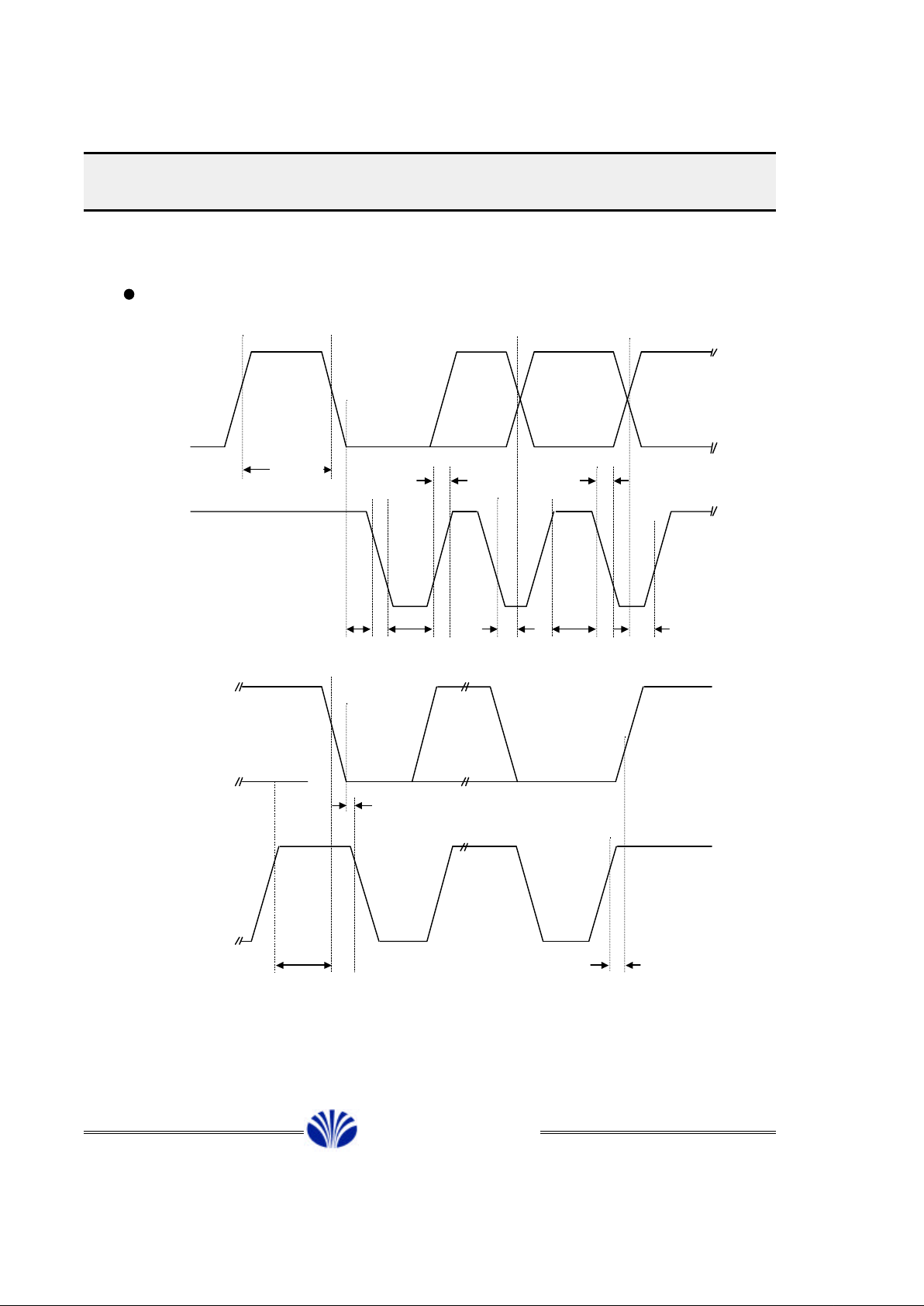
5.4 Interrupt Logic and External Interrupt
The internal interrupt logic for each of the five maskable interrupts for the DMC73C167
is shown in Figures 5-1 and 5-2 below. This interrupt logic will detect the output of each
corresponding interrupt.
Figure 5-1. Interrupt Logic (n = 2 or 4 ; m = 0 or 1)
£Ä£Á£Å£×£Ï£Ï
DAEWOO ELECTRONICS CO., LTD.
R
S
Q
INTn_mC
INTn_m
Input
INTn_mE
INTnF
Read
Interrupt Enable
(ST : Status Register)
INTn
Happen
Write
Read
Enable Latch
INTn Enable
INTnE
QD
InmFLG
Read
Page 35

35
8Bit Single Chip Microcontroller DMC73C167
The interrupt flag (INTn-mF) is set to 1 by the INTn_m input. The INTnF flag becomes active
when INTnE is 1, then INTn occurs if the interrupt enable bit (I bit) of the status register is
set to 1.
Figure 5-2. External Interrupt Logic (n = 1, 3 or 5 ; m = 0)
To conserve the low power requirement, one low-power mode - the HALT MODE - is provided.
It is invoked by executing an IDLE instruction. An external interrupt will release the device from
the low-power mode depending on whether it is in the HALTmode. When an external interrupt
is first asserted, its level is gated into an interrupt flag. In order for an interrupt signal to be
detected, the pulse duration must be a minimum of five internal clock cycles.
The INTn Enable bit is used separately to individually mask interrupt levels, and must be set 1
for the interrupt to be recognized.
As Previously stated, all interrupt control bits are implemented in the IOCTL0, IOCTL1, IOCTL2,
IOCTL3, and IOCTL4 registers in the peripheral file. I/O instructions may simply read from and
write to each INTn Enable bit. By the INTn input, the interrupt flag is set to 1 at the falling or
rising edge and becomes active when an interrupt is enabled.The interrupt service routine is
executed after the currently executing instruction is completed. Once the interrupt has been
acknowledged by the CPU, the CPU then pushes the contents of the status register and the
program counter (MSB and LSB), respectively, onto the stack and makes zero the status
register (see Section 4.4). The corresponding vector address is loaded into the program
counter, and the interrupt service routine is executed. The external interrupts, INT1, INT3_0,
and INT5_0, have Schmitt-trigger inputs and can be used as zero-cross detectors.
Because the pins can be used as both external interrupt pins and general-purpose I/O pins,
the following points should be noted :
D Q
Write
Read
Enable Latch
D Q
Write
Read
Enable Latch
CL
S
Q
InmCLR
EXTINTn
(SCHIMITT)
SENSnm
InmFLG
Read
InmENA
INTnE
INTn
Happen
Interrupt Enable
(ST : Status Register)
Read
INTnF
INTn Enable
£Ä£Á£Å£×£Ï£Ï
DAEWOO ELECTRONICS CO., LTD.
Page 36

36
8Bit Single Chip Microcontroller DMC73C167
1) The port using as the interrupt input should be in the input mode. The output mode may
cause damage to the device. If the contents of the corresponding output port are changed
from 1 to 0, the interrupt flag will also set to 1.
2) If not used as the interrupt input, the corresponding interrupt enable should be disabled.
But even with the disabling of this interrupt enable, the interrupt flag will be changed.
The external interrupt timing is shown in Figure 5-6. The device needs additional circuitry
when INT1, INT3_0, and IN 5_0 are used as zero-cross detectors as shown in Figure 5-7.
The following conditions are needed :
1) The external interrupt level should be in the range from VCC +0.3V to VSS. The input
current must not exceed the specification.
2) Noise on the interrupt signal should be minimized because the noise debounce logic is not
implemented on chip. The function may fail due to continuous interrupts.
Caution :
It is possible that the INTn flag bits in the IOCNT registers could be unintentionally cleared by
using bit manipulation instructions (ANDP/ORP & XORP). To avoid these occurences, use
the MOVP and STA instructions when writing Data to IOCNT registers.
Figure 5-3. External Interrupt Timing
VCC
VSS
External
Input
VT+
VT-
Interrupt
Happen
Last
Happen
1
0
Interrupt
Execution
£Ä£Á£Å£×£Ï£Ï
DAEWOO ELECTRONICS CO., LTD.
Page 37

37
8Bit Single Chip Microcontroller DMC73C167
Figure 5-4. Additional Circuit for External Input
5.5 Programmable Timer / Event Counter
The DMC73C167 has three on-chip programmable timers with individual start/stop
control bits. Timer 1 (shown in Figure 5-5) is a 16-bit timer. It has a 16-bit capture latch and
a 5-bit nonreadable prescaler with a 5-bit reload register. Timer 2 and Timer 3 (shown in
Figures 5-6 and 5-7) are 8-bit timers. They have an 8-bit capture latch and a 2-bit nonreadable
prescaler with a 2-bit reload register.
Table 5-17. Timer Mode and Clock Sources
Timer Mode Clock Source Capture Latch
Interrupt
Control
Trigger Register
RTC mode Internal Fosc/4 Port A3 (INT1) INT2_0 T1MSD (P20)
1 T1LSD (P21)
Event counter External port A1 active edge † T1CTL0 (P22)
mode T1CTL1 (P23)
2 RTC mode Internal Fosc/4 Port A4 (INT3_0) INT2_1 T2DATA (P24)
Event counter mode
External port A2 active edge† T2CTL (P25)
3 RTC mode Internal Fosc/4 Port A5 (INT5_0) INT3_1 T3DATA (P26)
Cascade Timer 2 underflow active edge† T3CTL (P27)
† Note : This active edge is determined by the INT1, INT3_0, and INT5_0 EDGE bit of
the IOCTL2 (P2) register.
VCC
VSS
Register
Input
Diode
Diode
DMC73C167
INT1
INT3_0
INT5_0
£Ä£Á£Å£×£Ï£Ï
DAEWOO ELECTRONICS CO., LTD.
Page 38

38
8Bit Single Chip Microcontroller DMC73C167
5.5.1 Timer 1
Figure 5-5. Timer 1 Schematic Diagram
Timer 1 is a 16-bit timer that contains a 5-bit prescaler and a 16-bit decrementer. The clock
source of Timer 1 is determined by bit 5 of T1CTL0 (T1SRC, P22.5).
Writing 0 to the T1SRC bit selects the internally generated Fosc/4 clock and places the timer/
event counter in real-timer clock mode. A T1SRC bit of 1 selects the external clock source
and places the timer/event counter in event counter mode.
Bit 7 of the T1CTL0 register is the START bit for Timer 1. When 0 is written to the START
bit, the timer chain is disabled or frozen at the current count value. When 1 is written to the
START bit, regardless of whether it was previously a 0 or a 1, the prescaler and counter
decrementers are loaded with the corresponding latch values and the timer/event counter
operation begins.
When the prescaler and counter decrement through zero together, an interrupt flag is set,
and the prescaler and counter decrementers are immediately and automatically reloaded
with the corresponding latch values of the reload registers.
The interrupt level generated by Timer 1 is INT2_0. Timer 1 has a 16-bit capture latch
associated with INT1(A3) that captures the current value of the counter whenever INT1 (port
A3) is activated.
5.5.1.1 Timer 1 Control Registers
Table 5-18. P20 0114h T1MSD Timer 1 MSB Data
Bit 7 6 5 4 3 2 1 0
R 16-bit Timer 1 MSB Decrementer Value
W 16-bit Timer 1 MSB Reload Register
£Ä£Á£Å£×£Ï£Ï
DAEWOO ELECTRONICS CO., LTD.
Pin A1
(I/O Port A1)
Prescaler
Reload
Register
16-bit
Reload
Register
5-bit
Prescaler
Fosc/4
T1SRC START
Capture Latch
A3 (External INT1)
Timer 1
Interrupt
(INT2_0)
Toggle Out
Normal
Port Out
Pin B0
T1OUT
16-bit
Decrementer
Page 39

39
8Bit Single Chip Microcontroller DMC73C167
Table 5-19. P21 0115h T1LSD Timer 1 LSB Data
Bit 7 6 5 4 3 2 1 0
R 16-bit Timer 1 LSB Decrementer Value
W 16-bit Timer 1 LSB Reload Register
Table 5-20. P23 0117h T1CTL1 Timer 1 Control 1
Bit 7 6 5 4 3 2 1 0
R MSB Capture Latch Value
W Invaild
Table 5-21. P22 0116h T1CTL0 Timer 1 Control 0
Bit 7 6 5 4 3 2 1 0
R Timer 1 LSB Capture Latch Value
W START T1OUT T1SRC Prescaler Reload Register
Read : Provides the LSB value of the capture register which contains the
decrementer register value when INT1 was last activated.
Write : Timer 1 control as below.
Bits 0-4 Reload the 5-bit Prescaler Reload Register
Bit 5 T1SRC. Select Timer 1 Clock Source.
0 = Internal clock (Fosc/4).
1 = External clock from Port A1.
Bit 6 T1OUT. Timer 1 Toggle Output
0 = Normal output on Port B0.
1 = Toggle output on Port B0 when the Timer 1 MSB decrementer
passes through zero.
Bit 7 START. Timer 1 Start/Stop Control
0 = Stops Timer 1
1 = Starts Timer 1
5.5.1.2 Real-Time Clock Mode (RTC)
In real-time clock mode, the internal Fosc/4 is the prescaler clock source. Each positive
pulse transition of the Fosc/4 period signal decrements the count chain.
£Ä£Á£Å£×£Ï£Ï
DAEWOO ELECTRONICS CO., LTD.
Page 40

40
8Bit Single Chip Microcontroller DMC73C167
5.5.1.3 Event Counter Mode (EC)
When Timer 1 is in event counter mode, port A1 is the clock source for Timer 1.
The maximum clock frequency on A1 at the event counter mode must not be greater than
Fosc/4. The minimum pulse width must not be less than 2/Fosc. Each positive pulse
Transition decrements the counter chain.
5.5.1.4 Timer 1 Interrupt Period
The period of the timer INT2_0 interrupt can be calculated as follows.
tINT = tCLK x (PL + 1) x (TL +1)
where :
tINT = period of timer interrupt
tCLK = 4/Fosc. for the internal real-time clock mode or the period of the input
clock source at the external EC mode
PL = Prescaler latch value (00h-1Fh : 5-bit)
TL = Decrementer reload value (0000h-FFFFh : 16-bit)
Example min : 1us
(Fosc : 4MHz) max : 2.097 sec
5.5.1.5 Capture Latch
The current value of the decrementer is stored in the capture latch register at the active
edge of Port A3. The active edge is determined by the INT-1 EDGE bit of the IOCTL2 (P2.1)
register. The capture latch is desabled during the IDLE instruction.
5.5.1.6 Timer Output Function
A timer output function exists on Timer 1 that allows the B0 output to be toggled every timer
decrements through zero. This function is enabled by the T1OUT bit of the timer control
register (T1CTL0.6). When operating in the timer output mode, the B0 output cannot be
changed by writing to the B port data register. Writing to the timer's START bit will reload
and start the timer but will not toggle the output. The output will toggle only when the timer
decrements through zero. The timer output feature is independent INT2_0 and therefore
will operate whether or not INT2_0 is enabled.
Whenever the T1OUT bit is returned to 0, B0 will become the normal output port. The value in
the B0 data register will be the last value output by the timer output function, and the CPU
can control the B0 data.
£Ä£Á£Å£×£Ï£Ï
DAEWOO ELECTRONICS CO., LTD.
Page 41

41
8Bit Single Chip Microcontroller DMC73C167
5.5.1.7 Notes on Timer Usage
In Timer 1, the most significant byte (MSB) read-out latch is shared between the MSB of the
decrementer and the MSB of the capture latch to be sampled at one moment. The Timer 1
MSB read-out latch can be read from both P20 and P23. Reading the LSB of the decrementer
or capture latch will always update the contents of the read-out latch. In order to read correctly
the entire 16-bit value of the decrementer or capture latch, the LSB must be read first, which
will load the MSB read-out latch. The MSB read-out latch must be read and stored after
reading the LSB of either the decrementer or capture latch.
5.5.2 Timer 2 / Timer 3
Timer 2 and Timer 3 are 8-bit timers that contain a 2-bit prescaler and an 8-bit decrementer.
The clock source of Timer 2 is determined by the T2SRC bit of the T2CTL register (P25.5),
and the clock source of Timer 3 determined by the T3SRC bit of the T3CTL register (P27.6).
Setting the T2SRC or T3SRC bits to 0 selects the internally generated Fosc/4 clock and
places the timer in real-time clock mode. Setting the T2SRC bit to 1 selects the external clock
source and places Timer 2 in event counter mode. Setting the T3SRC bit to 1 selects the
Timer 2 underflow for the Timer 3 clock source, and makes Timer 2 and Timer 3 cascadable.
When 0 is written to the START bit, the timer chain is disabled or frozen at the current count
value. When 1 is written to the START bit, regardless of whether it was previously a 0 or a 1,
the prescaler and counter decrementers are loaded with the corresponding latch values,
and the timer/event counter operation begins.
When the prescaler and counter decrement through zero thogether, an interrupt flag is set,
and the prescaler and counter decrementers are immediately and automatically reloaded
with the corresponding latch values.
The interrupt levels generated by the timers are INT2_1 for Timer 2 and INT3_1 for Timer 3
Timer 2 and Timer 3 each have a respective associated 8-bit capture latch that captures
the current value of the counter whenever 8-bit capture latch that captures the current value
of the counter whenever Port A4 (INT3_0) for Timer 2 or Port A5 (INT5_0) for Timer 3 are
activated.
Figure 5-6. Timer 2 Block Diagram
£Ä£Á£Å£×£Ï£Ï
DAEWOO ELECTRONICS CO., LTD.
Pin A2
I/O Port A2/Event
Counter Clock Input
2-bit
Prescaler
Fosc/4
T2SRC
START(P25.7)
Capture Latch
External A4 Pin
INT3_0
Timer 2
Interrupt
(INT2_1)
Timer 3
Clock
8-bit
Decrementer
Page 42

42
8Bit Single Chip Microcontroller DMC73C167
Figure 5-7. Timer 3 Block Diagram
5.5.2.1 Timer 2 and Timer 3 Control Registers
Table 5-22. P24 0118h T2DATA Timer 2 Data
Bit 7 6 5 4 3 2 1 0
R 8-bit Timer Decrementer Value
W 8-bit Timer Reload Register
Table 5-23. P25 0119h T2CTL Timer 2 Control
Bit 7 6 5 4 3 2 1 0
R Capture Latch Value
W START T3OUT T2SRC Not Used Prescaler Reload
Read : Provides the value of the capture register which contains the latched value of
the decrementer register when INT3_0 was first activated.
Write : Timer 2 control as below.
Bits 0, 1 Reload the 2-bit Prescaler Reload Register.
Bits 2-4 Not used.
Bit 5 T2SRC. Select Timer 2 Clock Source.
0 = Internal clock (Fosc/4).
1 = External clock from Port A2.
Bit 6 TOUT. Timer 3 Toggle Output.
0 = Normal output on Port B1.
1 = Toggled output on Port B1 when the Timer 3 MSB decrementer
passes through zero
£Ä£Á£Å£×£Ï£Ï
DAEWOO ELECTRONICS CO., LTD.
Timer 2
Underflow
2-bit
Prescaler
Fosc/4
T3SRC
START(P27.7)
Capture Latch
External A5 Pin
INT5_0
Timer 3
Interrupt
(INT3_1)
T3OUT
Normal Out
Toggle Out
Pin B1
8-bit
Decrementer
Page 43

43
8Bit Single Chip Microcontroller DMC73C167
Bit 7 START. Timer 2 Start/stop Control
0 = Stops Timer 2.
1 = Starts Timer 2.
Table 5-24. P26 011Ah T3DATA Timer 3 Data
Bit 7 6 5 4 3 2 1 0
R 8-bit Timer Decrementer Value
W 8-bit Timer Reload Register
Table 5-25. P27 011Bh T3CTL1 Timer 3 Control
Bit 7 6 5 4 3 2 1 0
R Capture Latch Value
W START T3SRC Not Used Prescaler Reload
Read : Provides the value of the capture register which contains the latched value
of the decrementer register when INT3_0 was most recently activated.
Write : Timer 3 control as below.
Bits 0, 1 Rescaler Road. Reload the 2-bit Prescaler Reload Register.
Bits 2-5 Not used.
Bit 6 T3SRC. Select Timer 3 Clock Source.
0 = Internal clock (Fosc/4).
1 = Timer 2 underflow (Cascade mode)
Bit 7 START. Timer 3 Start/stop Control
0 = Stops Timer 3.
1 = Starts Timer 3.
5.5.2.2 Real-Time Clock (RTC)
In real-time clock mode, the internal Fosc/4 is the decrementer clock source. Each positive
pulse transition of the Fosc/4 period signal decrements the counter chain.
5.5.2.3 Event Counter (EC)
When Timer 2 is in event counter mode, port A2 (ECI2) is the decrementer clock source for
Timer 2. The maximum clock frequency on A2 in event counter mode must not be greater
than Fosc/4. The minimum pulse duration must not be less than 2/Fosc. Each positive pulse
transition decrements the counter chain. It is not possible for Timer 3 to be in event counter
mode.
£Ä£Á£Å£×£Ï£Ï
DAEWOO ELECTRONICS CO., LTD.
Page 44

44
8Bit Single Chip Microcontroller DMC73C167
5.5.2.4 Timer 2 and Timer 3 Interrupt Period
The Period of the timer interrupts INT2_1 and INT3_1 can be calculated as follows.
tINT = tCLK x (PL + 1) x (TL +1)
where :
tINT = period of timer interrupt
tCLK = 4/Fosc. for the internal real-time clock mode or the period of the input
clock source at the external EC mode
PL = Prescaler latch value (0h-3h : 2bit)
TL = Decrementer reload value (00h-FFh : 8bit)
- In case of not cascade (INT2_1 and INT3_1)
Example : min : 1us
(CPUCLK : 4MHz) max : 1.024ms
- In case of Timer 2 and Timer 3 cascade (INT3_1)
Example : min : 1us
(CPUCLK : 4MHz) max : 1.048sec.
5.5.2.5 Capture Latch
The current value of the decrementer is stored in the capture latch register at the active edge
of port A4 (INT3_0) for Timer 2 and port A5 (INT5_0) for Timer 3. The active edge is determined
by the INT3_0 EDGE and INT5_0 EDGE bits of the IOCTL2 register (P2). The capture latch
register is disabled during the IDLE instruction.
5.5.2.6 Timer Output Function
A timer output function exists on Timer 3 that allows the B1 output to be toggled every time
the timer decrements through zero. This function is enabled by the T3OUT bit of the T2CTL
register (P25.6). When operating in the timer output mode, the B1 output cannot be changed
by writing to the B port data register. Writing to the timer's START bit will reload and start the
timer but will not toggle the output. The output will toggle only when the timer decrements
through zero. The timer output feature is independent of INT3_1 and therefore will operate
whether INT3_1 enabled or not.
Whenever the T3OUT bit is returned to 0, B1 will become the normal output port. The value
in the B1 data register will be the last value output by the timer output function, and the CPU
can control the B1 data.
£Ä£Á£Å£×£Ï£Ï
DAEWOO ELECTRONICS CO., LTD.
Page 45

45
8Bit Single Chip Microcontroller DMC73C167
5.5.3 Warming-up Timer
A 14-bit counter (P33, P34) is used as a warming-up delay timer which supplies a stable
oscillation condition from the system halt mode. The system clock cannot be active before
the warming-up counter's underflow. Fosc/2 (system clock frequency) is the decrementer
clock source of the 14-bit warm-up counter. The delay time is programmable by changing
P33 (the 6-bit MS value) and P34 (the 8-bit LS value).
Caution :
Set P35 to 0 before executing the IDLE instruction to avoid the unreliable setting of the
warming-up timer value.
5.6 A/D Converter
The key features of the A/D converter are as follows.
Analog input : 1 channel (A0)
Analog input range : VCC to VSS
Conversion : Successive approximation conversion
Resolution : 4 bit
Conversion time :40 machine cycle
Figure 5-8. A/D Converter Function Diagram
5.6.1 Reference Values of A/D Conversion
The reference values of ADDATA are listed below. VSS and VCC are assumed to be 0 and
+5V, respectively.
£Ä£Á£Å£×£Ï£Ï
DAEWOO ELECTRONICS CO., LTD.
Pin A0
Analog
Comparator
4-bit D/A
Converter
4-bit
Data Register
VSS
VCC
A/D START (P16.Bit7)
Enable Analog Input
(P16.Bit0)
0
1
General Input A0
ADDATA (P17)
Page 46

46
8Bit Single Chip Microcontroller DMC73C167
ADDATA Voltage Ranges (V) ADDATA Voltage Ranges (V)
0 0.0000-0.1562 8 2.3437-2.6562
1 0.1562-0.4687 9 2.6562-2.9687
2 0.4687-0.7812 10 2.9687-3.2812
3 0.7812-1.0937 11 3.2812-3.5937
4 1.0937-1.4062 12 3.5937-3.9062
5 1.4062-1.7187 13 3.9062-4.2187
6 1.7187-2.0312 14 4.2187-4.5312
7 2.0312-2.3437 15 4.5312-5.0
5.6.2. A/D Converter Control / Data Registers
The specifications of the A/D converter control and data registers are shown as follows.
Table 5-26. P16 011h ADCTL A/D Control
Bit 7 6 5 4 3 2 1 0
R
W
START 0 0 0 0 0 0 ADENA
Bit 0 ADENA. Enable Analog Input
The ADENA control bit configures port A0 as either an analog input
channel or a logic input channel. When the bit is set to 1, port A0 can
be enabled for analog signal input. When the bit is set to 0, port A0 can
be enabled for logic level input.
0 = Pin A0 is a digital input port
1 = Pin A0 is an analog input port.
Note : Before the A/D converter operation starts, the ADENA bit should
be set to 1.
Bit 1-6 Should be set to 0.
Bit 7 START. A/D Converter Start/Stop Control Bit.
0 = Stops A/D Converter
1 = Starts A/D Converter
£Ä£Á£Å£×£Ï£Ï
DAEWOO ELECTRONICS CO., LTD.
Page 47

47
8Bit Single Chip Microcontroller DMC73C167
Table 5-27. P17 0111h ADDATA A/D Conversion Data
Bit 7 6 5 4 3 2 1 0
R Not used A/D Conversion Data
W Invalid
Bit 0-3 A/D Conversion Data
4-bit A/D conversion data is retrieved by the read operation.
The write operation is not available through this register.
Bit 4-7 Not used.
5.6.3 A/D Converter Operation
The A/D converter operation procedure is as follows.
1) Turn on the 14-bit PWM.
2) Set the ADENA bit (ADCTL register bit 0) to 1.
3) Set the START (ADCTL register bit 7) to 1. Then A/D conversion starts.
4) The conversion data is transferred to the ADDATA register after A/D conversion is
completed. It takes 40 machine cycles.
5) The ADDATA register can be read. If the START bit is set to 0 during A/D conversion, the
A/D converter operation is terminated after A/D conversion is completed. This timing is
shown in Figure 5-9 for single conversion and Figure 5-10 for continuous conversion.
There is no status flag, so user should wait 40 machine cycles.
Attention :
The 14-bit PWM should be runing before turning on the A/D conversion.
£Ä£Á£Å£×£Ï£Ï
DAEWOO ELECTRONICS CO., LTD.
Page 48

48
8Bit Single Chip Microcontroller DMC73C167
Figure 5-9. Single A/D Conversion.
Figure 5-10. Continuous A/D Conversion.
Stop
Start
Clear
START
(P16.Bit7)
Select
Data (1)
ADIN
(A0)
A/D Converter
Operation
ADDATA
(P17)
Conversion (1)
Transfer Data ADDATA
Conversion Data (1)Previous Conversion Data
40 Machine Cycle
Stop
Start
Clear
START
(P16.Bit7)
Select
Data (1)
ADIN
(A0)
A/D Converter
Operation
ADDATA
(P17)
Analog Data (2)
Transfer Data
Conversion Data (1)
Previous Conversion Data
40 Machine Cycle 40 Machine Cycle
Analog Data (3) Analog Data (4)
Conversion (1) Conversion (2)
Conversion (3)
Transfer Data
Conversion
Data (2)
£Ä£Á£Å£×£Ï£Ï
DAEWOO ELECTRONICS CO., LTD.
Page 49

49
8Bit Single Chip Microcontroller DMC73C167
5.7 I2C
The DMC73C167 contains a I2C master/slave transceiver hardware interface. The I2C bus
is a serial communication system, and requires serial data SDA and an associated data clock
SCL. As the chip is fully programmable by software, it can be used for master mode, slave
mode, and/or multi-master mode operations. Both the SCL and SDA pins are input and
open-drain output pins.
For the DMC73C167, the slave address is as follows.
A6 A5 A4 A3 A2 A1 A0 R/W
0 1 1 0
1
A1 A0
The hardware (pin) programmable address bits are A1 and A0.
Figure 5-11 I2C Block Datagram
Note : SDA, SCL = Open drain output, Schmitt input
I2C Clock=Min 1952Hz-Max 71.86KHz
(CPU CLK : 4MHz)
Master
Duty High
Counter
Duty Low
Counter
SCL
I2C Clock
I2C Clock for Slave
Master
Transmit Data
Receive Data
SDA
I2C Data
Digital Filter
Digital Filter
Slave
Transmit Data
Receive Data
Slave Address
£Ä£Á£Å£×£Ï£Ï
DAEWOO ELECTRONICS CO., LTD.
Page 50

50
8Bit Single Chip Microcontroller DMC73C167
5.7.1 Master Mode
5.7.1.1 Master Control Register
Table 5-28. P48 013h MCTL0 I2C Master Control 0
Bit 7 6 5 4 3 2 1 0
RW ACT - RSRT LODUTY MDIR NACK BCM1 BCM0
Bit 7 ACT. Activation of Start Condition (R/W)
On hardware reset, this bit will be 0. But just after this bit is set to 1, actual
transfer will start. Therefore, before writing 1 to this bit, MSTS, MDATA, HDC,
and LDC should be initialized first. As soon as the start condition is generated,
the ACT bit will be cleared automatically.
Bit 5 RSRT. Restart (R/W)
A data transfer is always terminated by a stop condition generated by the
master. However, if a master still wants to communicate on the bus or
change the data transfer direction, it can generate another start condition
and address the new slave without first generating a stop condition.
To do this, the bit can be set after keeping the following settings for more
than 4usec: ACT=0, BCM1=0, and BCM0=0. This bit will be reset
automatically just after the restart action is triggered.
Bit 4 LODUTY. Low-Duty Output (R/W)
0 = SCL (Serial clock) duty is dependent on the contents of the HDC and
LDC values.
1 = Enlarges the low duration time by three times the LDC value.
For example, if HDC:LDC=1:1, the SCL duty will be 1:3 if the LODUTY
bit is set.
Bit 3 MDIR. Master Data Direction (R/W)
0 = Transmits data to the slave device. The contents of MDATA will be
loaded onto the SDA line.
1 = Receiveds data from the slave device. The data from the SDA line will
be stored in the MDATA register. Regardless of the MDIR bit, the address
data is always transmitted to the SDA line by internal hardware.
Bit 2 NACK. No Generation of Acknowledgement (R/W)
A master receiver must signal the last data transfer cycle or the end of the
data transfer to the slave transmitter by not generating an acknowledgement
on the last byte clocked from the slave. Then the slave transmitter will release
the data line to allow the master to generate the stop condition.
0 = Generates an acknowledgement after one byte has been received.
1 = Does not generate and acknlowledgement after one byte has been received.
£Ä£Á£Å£×£Ï£Ï
DAEWOO ELECTRONICS CO., LTD.
Page 51

51
8Bit Single Chip Microcontroller DMC73C167
Bit 1, 0 BCM 1,0 . Bus Mode 1 and Mode 0 (R/W)
When ACT = 1, these bit will be decoded as follows.
BCM1 BCM0
0 0 1 byte data transfer with every ACT = 1
1 0 Address output with start condition to salve.
0 1 Stop condition will be generated (no data transfer).
1 1 Prohibited for any case.
Table 5-29. P49 0131th MCTL1 I2C Master Control 1
Bit 7 6 5 4 3 2 1 0
R ENABLE X X X X SCLP SCLSDA X
W 0 0 0 0 0 0 0
Bit 7 ENABLE. Enables I2C Master Hardware (R/W)
0 = Stops I2C master hardware. This is same as H/W reset for I2C master module.
1 = Starts I2C master hardware.
Bit 2 SCLP (READ). SCL Port Input Data of I2C Bus.
0 = Logic low (0) level of SCL port.
1 = Logic high (1) level of SCL port.
Bit 1 SCLSDA (READ).
NAND gate buffered data of SCL, SDA port.
0 = Both SCL and SDA ports at high levels.
1 = At least one of SCL or SDA is at low level.
Bit 6-0 (WRITE). These bits should always be zero.
Note : In the multi-master mode, the ENABLE bit should be set to 1 before the
start condition comes up from another master device.
Table 5-30. P57 0139h DFCTL I2C Digital Filter Control
Bit 7 6 5 4 3 2 1 0
R DFON 0 Not Used
Bit 7 DFON. Digital Filter Control ON (R/W)
Narrow pulses on the SDA and SCL lines are rejected when the DFON bit is set to 1.
This bit is commonly used for master and slave operations.
0 = Digital Filtering Off.
1 = Digital Filtering On.
Note : Do not set the DFON bit to 1 if the higher period of the SCL is less than 8us
(Spec: min 4us + Filter; max 4us). Please set to "0" for normal usage.
£Ä£Á£Å£×£Ï£Ï
DAEWOO ELECTRONICS CO., LTD.
Page 52

52
8Bit Single Chip Microcontroller DMC73C167
Bit 6-0 Reserved. These bit should always be zero.
Table 5-31. P50 0132h MSTS I2C Master Status
Bit 7 6 5 4 3 2 1 0
R INT5_1F ALOST BERR BBUSY Not Used
W INT5_1C CLOST CBERR - Not Used
Bit 7 INT5_1F. I2C Master Interrupt (INT5_1) Flag. (READ)
After every action is completed, this bit will be set and INT5_1 interrupt is requested
if it is enabled. This bit is set on the following condition and reset by writing 1 to
INT5_1C. In order to proceed to the next sequence, this bit must be cleared first by
writing 1 to the INT5_1C bit.
- When completed to output address data on I2C.
- 1 byte of data is transferred.
After generation of stop condition.
- When there is a I2C bus error or arbitration is lost.
INT5_1C. Clear I2C Master Interrupt (INT5_1) Flag. (WRITE)
0 = No effect.
1 = Clears I2C master interrupt (INT5_1) flag.
Bit 6 ALOST. Bus Arbitration Lost. (READ)
When a transfer is initiated while the I2C bus is busy, ALOST will be set, and the
transfer will be canceled. If the master loses arbitration during the addressing or
data transfer stages, it will stop the SDA line drive and set the ALOST bit.
0 = Normal operation.
1 = Bus arbitration is lost.
CLOST. Clear Arbitration lOst Flag. (WRITE)
0 = No effect.
1 = Clears arbitration lost flag.
Bit 5 BERR. Bus Error. (READ)
During a data transmission or address cycle, a no acknowledgement response will
set this bit.
0 = Normal operation.
1 = A bus error has occurred.
CBERR. Clear Bus Error Flag. (WRITE)
During a data transmission or address cycle, a no acknowledgement response will
0 = No effected.
1 = Clears bus error flag.
Bit 4 BBUSY. Bus Busy. (READ)
A start condition will set this bit, and a stop condition or master reset will clear it.
0 = I2C bus is idle.
1 = I2C bus is either busy internally or being used by another master device.
£Ä£Á£Å£×£Ï£Ï
DAEWOO ELECTRONICS CO., LTD.
Page 53

53
8Bit Single Chip Microcontroller DMC73C167
Table 5-32. P51 0133h MDATA I2C Master Data
Bit 7 6 5 4 3 2 1 0
R Master Receive Data
W Master Receive Data
Bit 7-0 MDATA. 8-Bit Parallel Read/Write Shift Register.
The receiving data will be read every time INT5_IF=1. Afterwards, the INT5_1F flag
should be cleared. The transmitting data will be written every time INT5_1F=1.
Afterwards, the INT5_1F flag should be cleared.
Table 5-33. P52 0134h HDC I2C Master High Duration
Bit 7 6 5 4 3 2 1 0
R SCL High Duration Value
W SCL High Duration Value
Table 5-34. P53 0135h LDC I2C Master Low Duration
Bit 7 6 5 4 3 2 1 0
R SCL Low Duration Value
W SCL Low
Duration Value
HDC and LDC. SCL High and Low Duration Counters.
These are 8-bit registers for SCL frequency control By changing the contents of
these registers, the serial clock frequency (SCL) can be changed. High or low
duration can be calculated by the following equations.
High Duration = 4 x (FFh - Value of HDC) + 8
Fosc (OSC frequency of CPU)
Low Duration = 4 x (FFh - Value of LDC) + 8
(LODUTY = 0) Fosc (OSC frequency of CPU)
Low Duration = 3 x 4 (FFh - Value of LDC) + 8
(LODUTY = 1) Fosc (OSC frequency of CPU)
US
US
US
£Ä£Á£Å£×£Ï£Ï
DAEWOO ELECTRONICS CO., LTD.
Page 54

54
8Bit Single Chip Microcontroller DMC73C167
SCLK
Calculation example of SCL clock speed (Fosc:4MHz)
(1) MOVP %F9h, HDC
FFh-F9h = 6
(4x6+8)/ 4 = 8 so high duration
will be 8us
(2) MOVP %F9h, LDC
FFh - F9h = 6
(4x6+8) / 4 = 8 so low duration will
be 8us; but if DTY = 1,
low duration will be 20us
Notes:
1) By calcuration, any value can be selected except the following two values:
FFh, FEh (by design specifications).
2) The I2C bus minimum timing specification must be kept. The minimum
high/low duration is 4.0/4.7us, respectively.
3) The digital filter is contained for special user. Please set "0" for normal usage.
4) The HDC (P52) and LDC (P53) registers are not able to be read from and
written to if the ENABLE bit (P49, bit 7) is not set to 1.
5.7.1.2 Master Mode Operation
Any transfer will begin with a start condition and terminate with a stop condition.
After the start condition is generated, a slave address (the contents of MDATA) is
sent. This address is 8 bits long. Bit 0 indicates the data direction: 0 = write to slave
and 1 = read from slave. Following the address, 8-bit data is transferred as required
and then terminated by a stop condition generated by the master. However, if the
master still wants to communicate on the bus, it can generate another start condition
and address another slave without generating a stop condition (restart condition).
Various combinations of read/write formats are then possible within such a transfer.
On the DMC73C167, a hardware reset clears all bits of the master control and
status registers. To start data transfer, HDC and LDC must be set with the desired
value, and the ENABLE bit must be set to 1. The following are I2C master mode
control examples of data transfer operations.
Objective:
Send immediate hex data to Slave A: 88h, AAh
HD LD
£Ä£Á£Å£×£Ï£Ï
DAEWOO ELECTRONICS CO., LTD.
Page 55

55
8Bit Single Chip Microcontroller DMC73C167
Read two byte data from Slave B
Slave A address (0010001)
Slave B address (1010000)
a) Initialization of HDC/LDC, MCTL, and MDATA (Fosc.-4MHz)
MOVP %>80, MCTL1 Master I2C hardware on;
power-on reset routine
MOVP %>F9, HDC High duration will be 8us
MOVP %>F9, LDC Low duration will be 8us
MOVP %E0, MSTS Clear MSTS register
MOVP %?00100010, MDATA
Address out to Slave A
(write data to Slave A)
MOVP %?10100001, MDATA
Address out to Slave B
(read data from Slave B)
b) Start condition generation and address transfer
For start condition, set BCM1 (=1), BCM0 (=0) of MCTL0. The next data transfer
cycle is for write, so clear bit 3 (MDIR). To enable the start action, set ACT bit
(bit 7 of MCTL0).
MOVP %?10000010, MCTL0
After this instruction is executed, the I2C bus module will generate the start condition
and transfer 7 bits of address and 1 bit of direction information. After the address
cycle is completed, the I2C bus module will interrrupt the CPU. But if the CPU masks
the interrupt, the CPU must poll bit 7 (INT5_1F) of MSTS to check the address
transfer status.
c) Check status register (MSTS)
If the address transfer is completed successfully, the contents of MSTS will be 1001 ---(INT5_1F/ALOST/BERR/BBUSY/-). Then the INT5_1F bit should be cleared
before the next transfer.
(ACT/- /RSRT
/LODUTY /MDIR /NACK /BCM1 /BCM0)
1 0
0 0 0 1 0
£Ä£Á£Å£×£Ï£Ï
DAEWOO ELECTRONICS CO., LTD.
Page 56

56
8Bit Single Chip Microcontroller DMC73C167
MOVP %?10000000, MSTS
(BBUSY bit has not been touched)
d) Write transfer (two byte data)
MOVP %>88, MDATA Frist byte of data to be sent
MOVP %?10000000, MCTL0
After the interrupt or polling check of the INT5_1F bit, clear it by writing 1 to the
INT5_1C bit.
MOVP %?10000000, MSTS Clear INT5_1F bit
MOVP %>AA, MDATA Second byte of data to be sent
MOVP %?10000000, MCTL0
After the interrupt or polling check of the INT5_1F bit, clear the INT5_1F bit.
MOVP %?10000000, MSTS
(Clears INT5_1F bit)
e) Start condition generation and address transfer
To change the transfer direction or slave, a new cycle must be executed after the
current cycle is completed by generating a stop condition or invoking another start
condition. To generate another start condition, the RSRT and BCM1 bits of MCTL0
should be set after a 4us delay to keep the set up time of the start condition.
The next data transfer cycle is for read, so reset bit 3 (MDIR). To enable the start
action, set bit 7 (ACT) of MCTL0.
MOVP %?10100001, MDATA Reads data from Slave B
MOVP %?00100000, MCTL0 Second byte of data to be sent
WAITP BTJOP %?00000010,
MCTL1, WAITP
Waits until I2C bus if free
NOP One NOP will produce a 2.0 us delay
NOP
MOVP %>10100010, MCTL0
After this instruction is executed, the I2C bus module will generate a start condition
and transfer 7 bit of address and 1 bit of direction information. After the address
(ACT/- /RSRT
/LODUTY /MDIR /NACK /BCM1 /BCM0)
1 0
0 0 0 0 0
(ACT/- /RSRT /LODUTY /MDIR /NACK /BCM1 /BCM0)
1 0 0 0 0 0 0
(ACT/- /RSRT
/LODUTY /MDIR /NACK /BCM1 /BCM0)
0 1
0 0 0 0 0
(ACT/- /RSRT
/LODUTY /MDIR /NACK /BCM1 /BCM0)
1 1
0 0 0 1 0
£Ä£Á£Å£×£Ï£Ï
DAEWOO ELECTRONICS CO., LTD.
Page 57

57
8Bit Single Chip Microcontroller DMC73C167
cycle is completed, the I2C bus module will interrupt the CPU. But if the CPU masks
the interrupt, the following instruction can be used instead of the interrupt.
LOOP BTJZP %>80, MSTS, LOOP Repeats LOOP until INT5_1F is set
f) Clear INT5_1F bit and one byte read
MOVP %?10000000, MSTS Clear bit 7 of MSTS
MOVP %?10001000, MCTL0
When the two instruction above are executed, the I2C bus will receive one byte of
data from the slave. After the interrupt or checking the INT5_1F flag, the valid
one byte of data can be taken by reading MDR.
MOVP MDATA, A Stores read data into the A register
MOVP %?10000000, MSTS Clear bit 7 (INT5_1F) of MSTS
g) Last one byte read
MOVP %?10001100, MCTL0
After reading this byte, the I2C bus master should generate a stop condition. To do
this, it must send the message the "this is the last byte" by not generating the ACK
(nowledge) signal. This module does not generate the ACK signal by setting bit 2
(NACK) of MCTL0 to 1. After the interrupt or checking the INT5_1F flag, the
last one byte of data can be taken by reading MDATA.
MOVP MDATA, B Stores read data into the B register
MOVP %?10000000, MSTS Clear bit 7 (INT5_1F) of MSTS
h) Terminate transfer action (stop condition generation)
MOVP %?10000001, MCTL0
After generating the stop condition, the INT5_1F will be set. If needed, the interrupt
can be masked or this bit may not be checked. However, to begin another transfer
on the I2C bus, this bit should be cleared first.
(ACT/- /RSRT
/LODUTY /MDIR /NACK /BCM1 /BCM0)
1 0
0 1 0 0 0
(ACT/- /RSRT
/LODUTY /MDIR /NACK /BCM1 /BCM0)
1 0
0 0 0 0 1
£Ä£Á£Å£×£Ï£Ï
DAEWOO ELECTRONICS CO., LTD.
/BCM0)
(ACT/- /RSRT
/LODUTY /MDIR /NACK /BCM1
1 0
0 1 1 0 0
Page 58

58
8Bit Single Chip Microcontroller DMC73C167
5.7.2 Slave Mode
The DMC73C167 can be used as an I2C slave receiver and/or transmitter. The
slave address is not set by hardware but is programmable by software. There are
three peripheral registers for I2C slave operations: SCTL, SADDR, and SDATA.
5.7.2.1 Slave Control Registers
Table 5-35. P56 0138h SCTL I2C Slave Control
Bit 7 6 5 4 3 2 1 0
R ENABLE Not Used SEL SDIR GCALL INT5_2F
W Not Used INT5_2C
Bit 7 ENABLE. Enables I2C Slave Hardware (R/W).
Upon a hardware reset, this bit will be zero. After initialization of SADDR, this bit
can be set to enable the slave module. ENABLE is to be read from and written to
by software.
Bit 3 SEL. Device Selected (READ).
The general call address or address match will set this bit.
Bit 2 SDIR. Slave Data Direction (READ).
0 = Slave receiver (data read from I2C bus)
1 = Slave transmitter (data written to I2C bus)
Bit 1 GCALL. General Call.
0 = Normal
1 = Detects general call address.
Bit 0 INT5_2F. I2C Slave Interrupt Flag (READ).
This flag is identical to bit 5 of IOCTL4. The following cases will set INT5_2F and
generate an interrupt if enabled.
1) Slave transmitter mode (SDIR=1): Just after the slave address is selected (SEL=1)
2) Slave receiver mode (SDIR=0): The slave address is selected after receiving one byte.
3) After each byte of data is received or transmitted. But the interrupt will not be
generated after the last byte is transmitted because there will be no acknowledge
signal from the master.
INT5_2C. Clear I2C Slave Interrupt Flag (WRITE).
0 = No effected.
1 = Clears INT5_2 flag.
Notes:
1) Before clearing the INT5_2F bit, data must be read from or written to the
SDATA register.
2) The SCL will be pulled down when INT5_2F is set to high. But when it is cleared,
the SCL line will be released and can be controlled by the master device.
£Ä£Á£Å£×£Ï£Ï
DAEWOO ELECTRONICS CO., LTD.
Page 59

59
8Bit Single Chip Microcontroller DMC73C167
Table 5-36. P54 0136h SADDR I2C Slave Address
Bit 7 6 5 4 3 2 1 0
R - Not Used
W - 7-bit Slave Address
Bit 7 Not used.
Bit 6-0 7-bit Slave Address Register (READ/WRITE).
The Slave address register is programmable. This register must be set
with the appropriate value before the slave hardware logic is enabled,
that is before setting the ENABLE bit of SCTL.
Table 5-37. P55 0137h SDATA I2C Slave Data
Bit 7 6 5 4 3 2 1 0
R Slave Receive Data
W Slave Transmit Data
Bit 7-0 Slave Receive/Transmit Data (READ/WRITE).
The CPU can read or write parallel 8-bit data. During data transfer from/
to the I2C, data is shifted bit by bit. The receiving data will be read when
INT5_2F=1, after which the INT5_2F flag should be cleared. The transmitting
data will be written when INT5_2F=1, after which the INT5_2F flag should
be cleared.
5.7.2.2 Timing of Slave Mode Operations
5.7.2.2.1 Slave Receiver Mode
If the slave receives its slave address from the master, the contents of the P56 register
will be set to SEL=1/SDIR=0/GCALL=0/INT5_2F=0. If one byte of data is received,
the INT5_2F flag will be set, and the interrupt will occur. At that time the contents of
the P56 register will be set to SEL=1/SDIR=0/GCALL=0/INT5_2F=1. After that,
the INT5_2F flag will be set every time one byte of data is received.
This waveform shows the address cycle and the transfer of one byte of data during the
master transmitter mode (slave receiver mode). At the seventh SCL high, if the slave
address matches, the SEL bit will be set. At the eighth SCL high, the SDIR bit will be
set to zero, and after the eighth SCL falling, the slave will generate ACK on the SDA
line. On receipt of each byte of data from the master, the slave interrupt (INT5_2F)
is generated.
£Ä£Á£Å£×£Ï£Ï
DAEWOO ELECTRONICS CO., LTD.
Page 60

60
8Bit Single Chip Microcontroller DMC73C167
Figure 5-12. Data Transfer in Slave Receiver Mode
SCL
*Note
SDA
ACK by Slave
Start Condition SDIR(0) Set
SEL(1) Set
*Note
INT5_2F(1) Set
ACK by Slave
*Note : At this point INT5_1F is set when used as the master device.
5.7.2.2.2 Slave Transmitter Mode
If the slave receives its slave address from the master, the contents of the P56 register
will be set to SEL=1/SDIR=1/GCALL=0/INT5_2F=1. If the salve sends one byte of
data, one byte of data should be written to SDATA (P55) before the INT5_2F flag is
cleared. If the master returns ACK every time one byte of data is received from the
slave, the interrupt of the slave will occur. But if the master returns NACK to the slave,
the interrupt of the slave will not occur.
The accompanying waveform shows the address cycle and the transfer of one byte of
data during the master receiver mode (slave transmitter mode). At the seventh SCL
7-Bit Addr. & 1-Bit Dir.
12345678910101000
1 Byte Data from Master
12345678900101011
£Ä£Á£Å£×£Ï£Ï
DAEWOO ELECTRONICS CO., LTD.
Page 61

61
8Bit Single Chip Microcontroller DMC73C167
high, the SDIR bit will be set to 1, and after the eighth SCL falling, the slave will
generate ACK on the SDA line. After every address and data cycle, INT5_2F is set,
and the INT5_2 interrupt is generated when it is enabled.
Notes:
1) If ACK is not generated by the master (NACK) when one byte of data is transferred,
the slave interrupt will not occur. At that point the master should initiate a stop cycle
or a restart cycle.
2) The slave flags (SEL/SDIR/GCALL) except INT5_2F will be cleared after the
slave receives the stop condition or restart condition.
3) INT5_1F is set when this device is used as the master.
Figure 5-13. Data Transfer in Slave Transmitter Mode
SCLK
*See Note 3
SDA
INT5_2F(1)
Start Condition ACK by Slave
SDIR(1) Set
SEL(1) Set
*See Note 3
INT5_2F(1)
ACK by Master
7-Bit Addr. & 1-Bit Dir.
12345678910101001
1 Byte Data by Slave
12345678900101011
£Ä£Á£Å£×£Ï£Ï
DAEWOO ELECTRONICS CO., LTD.
Page 62

62
8Bit Single Chip Microcontroller DMC73C167
5.7.2.3 Slave Mode Operations
First the slave address must be set by writing the address value to SADDR. Then bit
7 (SMON) of SCTL must be set to turn on the slave module. When the slave module
is selected (via an address match or general call address), an interrupt will occur.
When this happens, the status bit (SDIR and GCALL) must be checked. If the master
wants to receive data from the slave module (SDIR=1), SDATA should be written
with the proper data, and then INT5_2F must be cleared.
The following instructions are an example of slave mode operations.
MOVP %21h, SADDR Slave address = 21h
MOVP %?10000001, SCTL (ENABLE/-----/INT5_2C)
1 1
LOOP BTJZP %01h, SCTL, LOOP Waits for INT5_2F = 1
BTJOP %02h, SCTL, ADD0 If GCALL = 1 does
special operation
BTJOP %04h, SCTL, SEND If SDIR = 1 sends data
to master
MOVP SDATA, A If SDIR = 0 receives
data from master
MOVP %?100000001, SCTL Clears INT5_2F flag
: (ENABLE/-----/INT5_2C)
: 1 1
:
SEND MOVP %AAh, SDATA If SDIR = 1 sends data
AAh to master
MOVP %?10000001, SCTL Clears INT5_2F flag
: (ENABLE/-----/INT5_2C)
: 1 1
:
ADD0 MOVP SDATA, B If GCALL = 1 reads data
from master
MOVP %?10000001, SCTL Clears INT5_2F flag
: (ENABLE/-----/INT5_2C)
: 1 1
:
Decodes contents of the B register
£Ä£Á£Å£×£Ï£Ï
DAEWOO ELECTRONICS CO., LTD.
Page 63

63
8Bit Single Chip Microcontroller DMC73C167
5.8 6-bit PWM (PWM1_0-PWM1_8)
5.8.1 Description of PWM1
The DMC73C167 microcontrollers feature nine PWM output ports.
Each port contains 6-bit resolution.
The ports are provided for the application of analog circuit control when combined
with an external low pass filter circuit. As shown in Figure 5-14, the 6-bit PWM is
composed of a 6-bit timer, two 6-bit latches, and two 6-bit comparators. When
started the 6-bit timer is filled up with 3Fh and increments during every period of
Fosc/16. The 6-bit timer is used for all 6-bit PWMs in common. For any of the nine
PWMs to start, the 6-bit timer must already be started. If the value of the 6-bit timer
is greater than a value of the latched 6-bit data, the comparator output is logic high
status.
Each PWM output port contains its own polarity control bit, which enables the port to
be selected as inverted or non-inverted output. If the PWM function is not required,
the port to be selected as inverted or non-inverted output. If the PWM function is not
required, the port could easily be used as a normal digital output port through polarity
control.
Notes:
PWM1_0-PWM1_8 ports are +12 V open-drain output.
£Ä£Á£Å£×£Ï£Ï
DAEWOO ELECTRONICS CO., LTD.
Page 64

64
8Bit Single Chip Microcontroller DMC73C167
Figure 5-14. 6-bit PWM Block Diagram
Polarity
Polarity
Fosc/16
The pulse width can be modulated by the minimum pulse with T0 depending on the
latched 6-bit data. The 6-bit data determines the duty of the PWM signal.
On-time = n (value of 6-bit data) x T0
One Cycle Time = 64 x T0 (256us at Fosc = 4MHz)
where: T0 = 16/Fosc (T0 = 4us at Fosc = 4MHz)
£Ä£Á£Å£×£Ï£Ï
DAEWOO ELECTRONICS CO., LTD.
6-Bit
On Time 0
6-Bit
Comparator 0
6-Bit
On Time 8
6-Bit
Comparator 8
6-Bit
Timer
PWM Output
PWM1_0 (Pin2)
1
PWM1_8
1
0
0
PWM1_1 (Pin3)
PWM1_2 (Pin4)
PWM1_3 (Pin5)
PWM1_4 (Pin6)
PWM1_5 (Pin7)
PWM1_6 (Pin8)
PWM1_7 (Pin9)
Page 65

65
8Bit Single Chip Microcontroller DMC73C167
Figure 5-15. 6-bit PWM Output Waveform
£Ä£Á£Å£×£Ï£Ï
DAEWOO ELECTRONICS CO., LTD.
On Time (n x T0)
Polarity : 1
: 0
One Cycle Time
(64 x T0)
Page 66

66
8Bit Single Chip Microcontroller DMC73C167
5.8.2 6-bit PWM Control Registers
Table 5-38. P37 0125h PWM1CTL 6-bit PWM Control
Bit 7 6 5 4 3 2 1 0
RW START 0 0 0 0 0 0 0
Bit 7 START. 6-bit PWM START (R/W).
0 = Stops 6-bit PWM counter.
1 = Starts 6-bit PWM counter.
Bit 6-0 Should be zero.
Table 5-39. P38 0126h PWM1_0T 6-bit PWM1_0 Time
Bit 7 6 5 4 3 2 1 0
R PWM1_0 Not Used
W POLE PWM1_0 OCR Value
Table 5-40. P39 0127h PWM1_1T 6-bit PWM1_1 Time
Bit 7 6 5 4 3 2 1 0
R PWM1_1 Not Used
W POLE PWM1_1 OCR Value
Table 5-41. P40 0128h PWM1_2T 6-bit PWM1_2 Time
Bit 7 6 5 4 3 2 1 0
R PWM1_2 Not Used
W POLE PWM1_2 OCR Value
Table 5-42. P41 0129h PWM1_3T 6-bit PWM1_3 Time
Bit 7 6 5 4 3 2 1 0
R PWM1_3 Not Used
W POLE PWM1_3 OCR Value
Table 5-43. P42 012Ah PWM1_4T 6-bit PWM1_4 Time
Bit 7 6 5 4 3 2 1 0
R PWM1_4 Not Used
W POLE PWM1_4 OCR Value
£Ä£Á£Å£×£Ï£Ï
DAEWOO ELECTRONICS CO., LTD.
Page 67

67
8Bit Single Chip Microcontroller DMC73C167
Table 5-44. P43 012Bh PWM1_5T 6-bit PWM1_5 Time
Bit 7 6 5 4 3 2 1 0
R PWM1_5 Not Used
W POLE PWM1_5 OCR Value
Table 5-45. P44 012Ch PWM1_6T 6-bit PWM1_6 Time
Bit 7 6 5 4 3 2 1 0
R PWM1_6 Not Used
W POLE PWM1_6 OCR Value
Table 5-46. P45 012Dh PWM1_7T 6-bit PWM1_7 Time
Bit 7 6 5 4 3 2 1 0
R PWM1_7 Not Used
W POLE PWM1_7 OCR Value
Table 5-47. P46 012Eh PWM1_8T 6-bit PWM1_8 Time
Bit 7 6 5 4 3 2 1 0
R PWM1_8 Not Used
W POLE PWM1_8 OCR Value
Bit 0-5 PWM1_n OCR. Output Compare Register.
This is a write-only register that defines the high or low output pulse width.
Bit 6 PWM1_n POLE. Polarity of PWM Output.
0 = Active low (port output is high when the OCR value is 0.)
1 = Active high (port output is low when the OCR value is 0.)
When PWM is stopped at each timing, the PWM output depends on the
polarity value (the value of bit 6).
Bit 7 Not used.
£Ä£Á£Å£×£Ï£Ï
DAEWOO ELECTRONICS CO., LTD.
Page 68

68
8Bit Single Chip Microcontroller DMC73C167
Figure 5-16. Timing and Polarity of 6-bit PWM1_0-PWM1_8 Output
Write BIT6 of P38 - P46
Start PWM Stop PWM
5.9 14-bit PWM (PWM0)
5.9.1 Description of PWM0
The periodic interval T = 5.4ms (FOSC = 6MHz) can be divided into 16k minimum
pulse width T0 = 333ns (FOSC = 6MHz), and the pulse width can be modulated by
the T0 unit depending on the 14-bit data. Also, by generating a small periodic interval
Ts = 85us (FOSC = 6MHz), which is 256 x T0, pulses of almost equal width can be
output with a period of Ts. Tm (m = 1 - 64), defined as the signal duration in 64 small
intervals, is calculated as follows. First, the 14-bit data is split into two parts: the most
significant 6 bits and the least significant 8 bits. The value of the LS 8 bits determines
the interval of basic time. Hence, Tm (1 - 64) = (number indicated by 8 bits) x T0 in
the 64 small intervals. Furthermore, the 6-bit data decides how many T0s are added
one by one in the 64 intervals. The relationship between the 6-bit data and Tm is
illustrated in Figure 5-24, and the basic 14-bit PWM waveform is shown in Figure 5-25.
On Time
0
1
BIT6
Value
On Time
1
0 : Low
0
After Reset
BIT6=0
PWM
£Ä£Á£Å£×£Ï£Ï
DAEWOO ELECTRONICS CO., LTD.
Page 69

69
8Bit Single Chip Microcontroller DMC73C167
Figure 5-17. 14-bit PWM Block Diagram
OR
£Ä£Á£Å£×£Ï£Ï
DAEWOO ELECTRONICS CO., LTD.
8 bit Comparater
PWM Output
14 bit PWM
Base Time (8 bit)
Polarity
14 bit PWM
Additional Time
(6 bit)
14 bit Timer
Additional
Pulse Generater
Fosc/2
Page 70

70
8Bit Single Chip Microcontroller DMC73C167
Figure 5-18. 14-bit PWM 1 Cycle and On Time
Small periodic interval Ts = 256 x T0 (128us:Fosc = 4MHz)
Base Time Tm = (value of 8-bit data) x T0
Additional time = T0
Where: T0 = 2/Fosc (T0 = 500ns at Fosc = 4MHz)
Table 5-48. 6-bit Data and Tm
6-bit Data (P36) Interval (T0) Adding Position
LSB
0 0 0 0 0 0 None
0 0 0 0 0 1 m = 32
0 0 0 0 1 0 m = 16, 48
0 0 0 1 0 0 m = 8, 24, 40, 56
0 0 1 0 0 0 m = 4, 12, 20, 28, 36, 44, 52, 60
0 1 0 0 0 0 m = 2, 6, 10, .........54, 58, 62
1 0 0 0 0 0 m = 1, 3, 5, .......... 59, 61, 63
Base Time
(Tm = Value of 8-bit Data x T0)
Polarity : 1
: 0
Small Periodic Interval
(Ts = 256 x T0)
Additional Time
(T0)
£Ä£Á£Å£×£Ï£Ï
DAEWOO ELECTRONICS CO., LTD.
Page 71

71
8Bit Single Chip Microcontroller DMC73C167
Figure 5-19. 14-bit PWM Output Waveform
256 x T0 = 128us
256 x T0 = 128us
5.9.2 PWM0 Control Registers
Table 5-49. P32 0120h PWM0CTL 14-bit PWM Control
Bit 7 6 5 4 3 2 1 0
RW START TEST Not Used POLE Not Used
Bits 0-2 Not Used
Bit 3 PWM0 POLE. PWM0 Polarity Control.
0 = Active low.
1 = Active high.
Bits 4, 5 Not Used
Bit 6 PWM0 TEST. For Test Mode Only.
Should always be 0.
Bit 7 PWM0 START.
0 = Stop PWM0.
1 = Run PWM0.
T1 T2 T64
6T0
6T0
6T0
6T0
T
Data 8 Bits (00000110) P36
Data 6 Bits (- -000000) P35
T1 T2 T32
6T0
7T0
6T0
6T0
Data 8 Bits (00000110) P36
Data 6 Bits (- -000001) P35
T64
£Ä£Á£Å£×£Ï£Ï
DAEWOO ELECTRONICS CO., LTD.
Page 72

72
8Bit Single Chip Microcontroller DMC73C167
Figure 5-20.
Write BIT3 of P32
Start PWM Stop PWM
Table 5-50. P35 0123h PWM0AT 14-bit PWM Add Time
Bit 7 6 5 4 3 2 1 0
R Not Used
W 14-bit PWM OCR Additional Value
Table 5-51. P36 0124h PWM0BT 14-bit PWM Base Time
Bit 7 6 5 4 3 2 1 0
R Not Used
W 14-bit PWM OCR Base Value
Note:
Smoothly any additional bit divides equally by 32 cycles when the bit is integrated.
Not Used
0
1
BIT3
Value
On Time
On Time
1
0 : Low
0
After Reset
BIT3=0
PWM Output
£Ä£Á£Å£×£Ï£Ï
DAEWOO ELECTRONICS CO., LTD.
Page 73

73
8Bit Single Chip Microcontroller DMC73C167
5.10 On Screen Display
The DMC73C167 on screen display (OSD) hardware has two separate video
RAM blocks called Line A and Line B. Both Line A and Line B can be accessed
by the CPU separately. Thus, it is possible to modify video RAM data while one
line is being accessed by the video display controller. So multiple lines are easily
displayed with the help of the display line counter which is supported by on-chip
hardware.
5.10.1. Major Features of the OSD Module
Number of display patterns 2 independent lines x 20 columns
(max of 12 lines by software control)
Number of character fonts 128
Character font structure 12 x 18
Character color 8 colors for each character
Character size x1 (20 columns), x4 (10 columns)
Horizontal position 2 dots/1 bit, 7 bits (max 256 dots move)
Vertical position 2H/1 bit, 8 bit
OSD interrupt counters 4bits, cleared by VSYNC
OSD interrupt sources INT4
£Ä£Á£Å£×£Ï£Ï
DAEWOO ELECTRONICS CO., LTD.
Page 74

74
8Bit Single Chip Microcontroller DMC73C167
Figure 5-21. OSD Functional block
5.10.2 OSD Control Registers
Table 5-52. P68 0144h OSDCTL OSD Control Register
Bit 7 6 5 4 3 2 1 0
RW START Not Used SIZE R G B
CHARACTER COLOR
Bit 7 START. OSD On/Off. (R/W)
0 = Stop.
1 = Start, Restart.
Bit 3 SIZE. Select Size. (R/W)
0 = Normal (1 x 1)
1 = Double (2 x 2)
£Ä£Á£Å£×£Ï£Ï
DAEWOO ELECTRONICS CO., LTD.
/Hsync
OSD
Clock
/Hsync
/Vsync
OSDHP(P69) OSDCTL(P68)
VRAM A
VRAM B
Horizontal Timing Generation
7
Hori
Posi
CNTR
7
Size On/Off
R,G,B
LINCNT(P72)
INT4
Vertical Timing Generation
CHAR ROM
Vert
Posi
CNTR
8
7
3
R,G,B
OSDVPA(P70) OSDVPB(P76)
8 8
Output
Control
R
G
B
Y
OSDBGCTL(P76)
12
3
R,G,
BG On/Off
3
(OTP Device only)
Page 75

75
8Bit Single Chip Microcontroller DMC73C167
Bits 2-0 Character Color. (R/W)
000 = Black
001 = Blue
010 = Green
011 = Cyan
100 = Red
101 = Magenta
110 = Yellow
111 = White
Table 5-53. P72 0148h LINCNT Current Display Line Designator
Bit 7 6 5 4 3 2 1 0
R Display Line Counter Value
W (User Write Not Allowed)
Note:
This is cleared at the falling edge of VSYNC or a hardware reset. It is incremented
by one after displaying one line, which occurs simultaneously with the OSD interrupt.
Table 5-54. P69 0145h OSDHP OSD Horizontal Position
Bit 7 6 5 4 3 2 1 0
RW Not Used Horizontal (X) Position
Horizontal (X) = Adjust position right or left 01h-7Fh
(2 dots/1 bit)
Table 5-55. P70 0146h OSDVPA OSD Vertical Position for Video RAM A
Bit 7 6 5 4 3 2 1 0
RW Vertical Position Data for Line A
Adjust position upper or lower 000h-FFh
(2H/1 bit)
Not Used
£Ä£Á£Å£×£Ï£Ï
DAEWOO ELECTRONICS CO., LTD.
Page 76

76
8Bit Single Chip Microcontroller DMC73C167
Table 5-56. P71 0147h OSDVPB OSD Vertical Position for Video RAM B
Bit 7 6 5 4 3 2 1 0
RW Vertical Position Data for Line B
Adjust position upper or lower 00 h-FFh
(2H/1 bit)
Character Font: 128 type. The Character color is set
with the character code data which consists of a total of 10 bits: 7 bits
(character font) + 3 bits (character color) for each character.
<Video RAM File> Note: (1)
Address Range Contents
0160h-0173h OSD A Line Character Address
0180h-0193h OSD B Line Character Address
Table 5-57. P67 0143h PRTCL OSD YOUT Polarity Control
Bit 7 6 5 4 3 2 1 0
RW POLRCTL Not Used
Bit 7 POLRCTL OSD YOUT Polarity.
0 = High active.
1 = Low active
£Ä£Á£Å£×£Ï£Ï
DAEWOO ELECTRONICS CO., LTD.
Page 77

77
8Bit Single Chip Microcontroller DMC73C167
5.10.3 OSD Interrupt and Operation
Before starting the display, the user should write the first line of display information to
video RAM A and OSDVPA, and write the second line of display data to video RAM
B and OSDVPB. Then set the START bit (bit 7 of OSDCTL) to turn on the OSD
module.
The OSD interrupt will occur when the condition causing the interrupt sets the interrupt
flag (bit 1 of IOCTL1) to 1 and when the interrupt enable bit (bit 0 of IOCTL1) is set
to 1 regardless of the OSD START bit (P68, bit 7). The interrupt flag will be set if
one of the following cases occurs:
- Vsync falling
- End point of each line of the display is reached
If the TV scan line comes to the value of OSDVPA, the first line A (video RAM A)
will be displayed. At the end point of the line A display (the last dot of the dots
making up the 20th character of line A), an interrupt will occur, and LINCNT will be
incremented by one. Thus, the user can read the value "01h" from LINCNT (which
designates the end of the first line of display).
From that point, the second line (line B) will start to display according to OSDVPB
(V-position counter B) value. At the same time, the user can change video RAM A
and OSDVPA (V-position counter A) with the data to be displayed on the third line.
After the second line is displayed, another OSD interrupt will occur, and the user can
read value "02h" from LINCNT. Then the display of the third line (the contents of
video RAM A) will commence with the new data input from the first interrupt routine.
As before, during this interrupt routine the user should write the proper data for video
RAM B and OSDVPB with the data to be displayed on the fourth line of the display.
A maximum of 12 lines can be displayed on the screen using this control method.
Regardless of the last video RAM used (A or B), after Vsync the first line of display
data will come from video RAM A and OSDVPA.
To display only one line, write "FFh" to OSDVPB. As before, when the first line is
displayed the OSD interrupt will occur, and the LINCNT counter will have the value
"01h". No action is needed for that interrupt if you don't want to change the display
data.
£Ä£Á£Å£×£Ï£Ï
DAEWOO ELECTRONICS CO., LTD.
Page 78

78
8Bit Single Chip Microcontroller DMC73C167
5.10.4 OSD Programming Example
5.10.4.1 Multiple-Line Display
The following flow chart is an example of a four-line display. Regardless of whether
the display is an odd or even number of lines, the first line of data for any field to be
displayed on the screen will come from video RAM A and OSDVPA.
Figure 5-22. Example Flow Chart of 4 Line Display
- DO NOTHING
- DO NOTHING
- OSDVPB
- VIDEO RAM B
- OSDVPA
- VIDEO RAM A
- OSD OFF
- OSDVPA
- VIDEO RAM A
- OSDVPB
- VIDEO RAM B
- OSD ON
IF LINECNT = 0
IF LINECNT = 1
IF LINECNT = 2
IF LINECNT = 3
IF LINECNT = 4
RETI
V-Position for 1st line
Data to be displayed
V-Position for 2nd line
Data to be displayed
- V-Position for 3rd line
- Data to be displayed
- V-Position for 4th line
- Data to be displayed
OSD INTERRUPT
£Ä£Á£Å£×£Ï£Ï
DAEWOO ELECTRONICS CO., LTD.
Page 79

79
8Bit Single Chip Microcontroller DMC73C167
5.10.4.2 One-Line Display
- OSD OFF
- OSDVPA V-Position for 1st Line
- VIDEO RAM A Data To Be Displayed
- OSDVPB FFh
- OSD ON
- DO NOTHING
Figure 5-23. Video RAM and CPU Interface
OSD INTERRUPT
IF LINECNT = 0
IF LINECNT = 1
RETI
£Ä£Á£Å£×£Ï£Ï
DAEWOO ELECTRONICS CO., LTD.
Char ROM Addressing
Colors
3
7
OSDCTL
Character Address
CPU Data Bus
Character Color
Display Counter
DIN 9 - 0
M
P
X
CPU Addr
1st Char Address
2nd Char Address
.
.
.
.
Video RAM
.
.
.
.
40th Char Address
OSD Addr
160h
161h
.
.
.
.
173h
180h
181h
.
.
.
193h
8
7
3
Page 80

80
8Bit Single Chip Microcontroller DMC73C167
Figure 5-24. Character ROM and Character Assignment
Output
Controller
12-Bit Shifter
0
12 x 18 Dots
1-Character Structure
...........................
...........................
...........................
...........................
...........................
.
.
.
.
...........................
...........................
Character ROM
7 Bits From
Video RAM
From
Video RAM
From Vertical
18-Dot Counter
Color
12
5
7
127
1
.
.
.
.
.
.
.
.
9
A
B
.
.
.
.
.
.
.
.
3
OSD Out
Video Timing
£Ä£Á£Å£×£Ï£Ï
DAEWOO ELECTRONICS CO., LTD.
Page 81

81
8Bit Single Chip Microcontroller DMC73C167
5.10.5 R, G, B, and Y Output Timing
R, G, B, and Y output timing are shown in the figures below.
Figure 5-25. R, G, B, and Y Output Timing
Notes:
1) R, G, B, and Y waveforms correspond to this line.
2) Even R, G, B, is low (color data is 0), Yout is activated when character font data is at
the display location (black color).
3) Yout and /Yout are mask option, which mean the option is placed on a manufacturing
template, or mask, that copies the actual circuit onto the silicon device. This means
the Yout option is finalized at the start of manufacture and cannot be changed by either
software or hardware. The Yout of (OTP) can be changed by software controls.
4) SE73CP87 supports the Yout signal only (active high only).
Note 1
1
***
***
*
*
*
*
*
*
*
*
*****
*
*
*
***
*
*
*
*
*
*********
*********
* *
***
* * *
* *
***
* * *
/Yout
Note 4
Note 2
0
1
1
0
Rout
0
1
Gout
1
0
Bout
0
Note 2
Note 3
Yout
DAEWOO ELECTRONICS CO., LTD.
Page 82

82
8Bit Single Chip Microcontroller DMC73C167
5.11 Low-Power Mode
The DMC73C167 supports the Halt mode as the Low-power mode.
This mode is entered when the IDLE instruction is executed.
Activating RESET or acknowledging an enabled interrupt releases the device from this mode.
This low-power mode freezes the I/O ports, retaining their conditions before the IDLE instruction
was executed.
Complete RAM data retention is also maintained through this low-power mode as power is applied.
Table 5-11 describes the low-power mode.
Table 5-59. Low-Power Mode
In this low-power mode, the A/D converter is stopped and the oscillator is halted.
Note : If you want to enter into Halt Mode, you must stop Timer1, Timer2 and Timer3 before executing
IDLE instruction.
DAEWOO ELECTRONICS CO., LTD.
MODE
HALT
OSC
HALTED
TIMER1
HALTED
TIMER3
HALTED
EXIT MODE VIA
RESET, INT1, INT3_0, INT5_0
TIMER2
HALTED
Page 83

83
8Bit Single Chip Microcontroller DMC73C167
6. OTP DEVICE SPECIFICATIONS
6.1 Pin Assignment of OTP Programming Adapter Board
The 73CE167 can be programmed like any TMS27C128 on a wide variety of EPROM programmers.
Programming the 73CE167 requires a 54-to-28 pin adapter socket with the XRESET and OSCIN
pins grounded.
The following diagram shows the connections that need to be made on the 54-to-28 pin socket.
Figure 6-1. Required Connections on 54-to-28 Pin Adapter Socket
20 XE PWM0 (14bit) 1 54 VCC VCC
28
PWM1_0 (6bit) 2 53 A7/POWER CTL A6
4
PWM1_1 (6bit) 3 52 SCL XG
22
PWM1_2 (6bit) 4 51 SDA XPGM
27
PWM1_3 (6bit) 5 50 A6 A5
5
PWM1_4 (6bit) 6 49 A5/INT5_0 A4
6
PWM1_5 (6bit) 7 48 A4/INT3_0 A3
7
PWM1_6 (6bit) 8 47 A3/INT1 A2
8
PWM1_7 (6bit) 9 46 A1/ECI1 A0
10
PWM1_8 (6bit) 10 45 /RESET GND
14
B0/T1OUT(OPEN D) 11 44 OSC OUT(CPU)
B1/T3OUT(OPEN D) 12 43 OSC IN(CPU) GND
14
B2(OEPN DRAIN) 13 42 TEST VPP
1
B3(OEPN DRAIN) 14 41 A2/ECI2 A1
9
3 A7 B4(OEPN DRAIN) 15 40 OSC OUT(OSD)
25 A8 B5(OEPN DRAIN) 16 39 OSC IN(OSD) GND
14
24 A9 B6(OEPN DRAIN) 17 38 /Vsync GND
14
21 A10 B7(OEPN DRAIN) 18 37 /Hsync GND 14
14 GND A0/4BIT ADC 19 36 Yout or /Yout
11 Q1 C0 20 35 BLUE
12 Q2 C1 21 34 GREEN
13 Q3 C2 22 33 RED GND VCC
15 Q4 C3 23 32 D3-CH/XUROM 14 OR 28 D S/W
16 Q5 C4 24 31 D2 A13 26
17 Q6 C5 25 30 D1 A12 2
18 Q7 C6 26 29 D0 A11 23
14 GND VSS 27 28 C7 Q8 19
SOCKET
PIN
T27C128
FUNC.
73CE167 PIN CONFIGURATION
T27C128
FUNC.
SOCKET
PIN
7
3
C
E
1
6
7
£Ä£Á£Å£×£Ï£Ï
DAEWOO ELECTRONICS CO., LTD.
Page 84

84
8Bit Single Chip Microcontroller DMC73C167
Notes : 1)
PWM1_(0 to 8), B (0 to 3), Yout, OSCOUT (OSD/CPU), BLUE, RED, GREEN ==> Open.
2) CHROM/XUROM (#32) = Low ==> 16K user EPROM
programming and read
= High ==> character EPROM
programming and read
3) For signature mode, insert a 3.9 Kohms resistor between the pin #24 of the socket and the
pin #17 of the 73CE167.
4) In R bit program and verify mode, #37 and #38 ==> VCC.
Table 6-1. 73CE167 Pin Assignments
Normal Mode EPROM Mode TMC27C128
Signal Pin No. I/O Description Signal I/O Description Name Pin No.
A0 19 I/O 4-bit ADC - A1 46 I/O ECI1 A0 I A0 10
A2 41 I/O ECI2 A1 I A1 9
A3 47 I/O INT1 A2 I EPROM A2 8
A4 48 I/O INT3 A3 I Address A3 7
A5 49 I/O INT5 A4 I A4 6
A6 50 I/O A5 I A5 5
A7 53 I/O A6 I A6 4
B0 11 O OPEN DRAIN (2 NTR) 12V - B1 12 O OPEN DRAIN (2 NTR) 12V - B2 13 O OPEN DRAIN (2 NTR) 12V - B3 14 O OPEN DRAIN (2 NTR) 12V - - EPROM
B4 15 O OPEN DRAIN (1 NTR) 5V A7 I Address A7 3
B5 16 O OPEN DRAIN (1 NTR) 5V A8 I A8 25
B6 17 O OPEN DRAIN (1 NTR) 5V A9 I A9 24
B7 18 O OPEN DRAIN (1 NTR) 5V A10 I A10 21
C0 20 I/O DO I/O Q1 11
C1 21 I/O D1 I/O Q2 12
C2 22 I/O D2 I/O Q3 13
C3 23 I/O Port C is a D3 I/O DO - D7 are Q4 14
C4 24 I/O bidirectional data port D4 I/O data I/O Q5 15
C5 25 I/O D5 I/O Q6 16
C6 26 I/O D6 I/O Q7 17
C7 28 I/O D7 I/O Q8 18
DO 29 I/O A11 I A11 23
D1 30 I/O Port D is a A12 I EPROM A12 2
D2 31 I/O bidirectional data port A13 I Address A13 26
D3 32 I/O CHROM/XUROM I
£Ä£Á£Å£×£Ï£Ï
DAEWOO ELECTRONICS CO., LTD.
Page 85

85
8Bit Single Chip Microcontroller DMC73C167
Normal Mode EPROM Mode TMC27C128
Signal Pin No. I/O Description Signal I/O Description Name Pin No.
RED 33 O - -
GREEN 34 O - -
BLUE 35 O - -
Yout 36 O Active Low - Hsync 37 I EPTESTHV I GND 14
Vsync 38 I EPTEST I GND 14
OSC1IN 43 I CPU CLK-IN GND I VSS GND 14
OSC1OUT 44 O CPU CLK-OUT
XRESET 45 I Device Reset GND I VSS GND 14
TEST 42 I Device Test VPP I PGM High Vtg VPP 1
PWM0 1 O 14-bit PWM XCE I XE 20
PWM1_0 2 O 6-bit PWM - PWM1_1 3 O 6-bit PWM - PWM1_2 4 O 6-bit PWM - PWM1_3 5 O 6-bit PWM - PWM1_4 6 O 6-bit PWM - PWM1_5 7 O 6-bit PWM - PWM1_6 8 O 6-bit PWM - PWM1_7 9 O 6-bit PWM - PWM1_8 10 O 6-bit PWM - -
OSC2IN 39 I OSD CLK-IN - -
OSC2OUT 40 O OSD CLK-OUT - -
I2C DAT 51 I/O I2C DATA (OPEN DRAIN) XPGM I XPGM 27
I2C CLK 52 I/O I2C CLK (OPEN DRAIN) XOE I XG 22
VSS 27 I VSS I VCC 28
VDD 54 I VDD I GND 14
Note 1 : Important Notice
A) EPTESTHV pin assigned to Hsync, and EPTEST pin assigned to Vsync.
EPTEST EPTESTHV OPERATION
0 0 PGM, PGM VERIFY, READ
1 0 WORD LINE STRESS, BIT LINE STRESS
1 1 OTHER FUNCTION TEST MODE
B) VPP pin assigned to TEST pad
C) ADDR (0 to 14) was assigned to APORT (1 - 7), BPORT (5 - 7), DPORT (0 - 3)
D) EPROM I/O data (8) was assigned to CPORT
Note 2 : EPROM-related Pins
DATA LINE 8 pins
ADDRESS 15 pins (ADDR0 - ADDR13, CHROM/XUROM)
CONTROL 5 pins (XCE, XOE, XPGM, EPTEST/HV)
VPP 1 pin
29 pins
Other Pins 4 pins (XRESET, OSCIN, VCC, VSS)
Total 33 pins
DAEWOO ELECTRONICS CO., LTD.
Page 86

86
8Bit Single Chip Microcontroller DMC73C167
6.1.1 Control Register of 73CE167 (OTP)
Table 6-1. P67 0143h Yout Polarity Control
Table 6-2. P77 014Dh APORT Pull-up TR Control Register
Table 6-3. P78 014Eh B/D PORT Pull-up TR Control Register
Yout
POLARIT
3
Yout Polarity. (R/W)
Value After Reset
Not Used
2
1
0
7 6 5 4
Bit
R
W
Bit 7
0 = No change High active.
1 = Changes polarity Low active.
DAEWOO ELECTRONICS CO., LTD.
76543210
00000000
A7
3
APORT Pull-up TR Control Data.
Value After Reset
2
1
07 6 5 4
Bit
R
W
A7 - A0
0 = Pull-up TR on.
1 = Pull-up TR off.
A2 A1 A0A5 A4 A3A6
B7
3
BPORT Pull-up TR Control Data.
2 1 07 6 5 4
Bit
R
W
B7 - B4
0 = Pull-up TR on.
1 = Pull-up TR off.
D2 D1 D0B5 B4 D3B6
DPORT Pull-up TR Control Data.D3 - D0
0 = Pull-up TR on.
1 = Pull-up TR off.
76543210
00000000
Value After Reset
76543210
00000000
Page 87

87
8Bit Single Chip Microcontroller DMC73C167
Table 6-4. P79 014Fh CPORT Pull-up TR Control Register
Note : After the reset values of the A/B/C/D pull-up control registers are all "00h", then all of pull-up TRs
(=47K ohm) are connected to each pin by default. If the pull-up TRs are not needed, write FFh at
P77, P78 and P79 to disconnect the pull-up TR first. Unwanted pull-up TRs can cause problems.
C7
3
CPORT Pull-up TR Control Data.
2
1
07 6 5 4
Bit
R
W
C7 - C4
0 = Pull-up TR on.
1 = Pull-up TR off.
C2 C1 C0C5 C4 C3C6
DAEWOO ELECTRONICS CO., LTD.
Value After Reset
76543210
00000000
Page 88

88
8Bit Single Chip Microcontroller DMC73C167
6.2 Package Descriptions (Mechanical Data)
Figure 6-2. 54-Pin Shrink Dual In-Line Package (SDIP)
[ UNIT : Milimeter ]
54
1 27
28
15°Max
51.60Max
54 SDIP
14.22Max
1.778 TYP
0.46±0.1
5.08Max
3.18Min
0.51Min
2.69Max
1.016±0.2
0.28±0.08
15.25 TYP
£Ä£Á£Å£×£Ï£Ï
DAEWOO ELECTRONICS CO., LTD.
Page 89

#
8Bit Single Chip Microcontroller DMC73C167
* Appendix : OSD Font Design Guide
1. OSD Font Create Rules for CTV Controller
Subject : OSD Font Format for CTV Controller
Caution : User should make OSD fonts according to the following rules.
Rule 1. User should only use dot (.) or the asterisk (*) to make the OSD font.
The dot (.) represents ROM data '0' and asterisk (*) represents ROM data '1'
respectively.
Other symbols (except . and *) should not be permitted.
Rule 2. This Device has two OSD font types.
The font (Fig. 1) should be made by horizontal 12 symbol x vertical 18 symbol.
Don't be perimitted to contain space or other symbol (except . and *) in a OSD font.
Figure 1. OSD Font Form (Example)
...........................******.....********...***....***..**......**..**......**..**......**..**......**..**......**..**......**..**......**..**......**..***....***...********.....******..........................
.
Rule 3. Between font to font horizontal space is permitted only one space.
Between font to font verical space is permitted only one space and only one
custom comment line as shown (Fig.2)
Rule 4. This device has as following font numbers.
128 font + 2 dummy font : 5 char x 26 (Fig. 2)
Rule 5. Outside of OSD font area should not be included any symbols.
£Ä£Á£Å£×£Ï£Ï
DAEWOO ELECTRONICS CO., LTD.
Page 90

#
8Bit Single Chip Microcontroller DMC73C167
Figure 2. OSD Font File made by user
Horizontal Total : 60 Dots / Asterisks + 4 Spaces
12 Dots +- 1 Space +- 1 Space +- 1 Space +- 1 Space
>00 >01 >02 >03 >04
Comment Line
. . . . . . . . . . . . . . . . . . . . . . . . . . . . . . . . . . . . . . . . . . . . . . . . . . . . . . . . . . . .
. . . . . . . . . . . . . . . . . . . . . . . . . . . . . . . . . . . . . . . . . . . . . . . . . . . . . . . . . . . .
. . . * * * * * * . . . . . . . . * * . . . . . . . . * * * * * * . . . . . . * * * * * * . . . . . . . . . . * * . . .
. . . * * * * * * . . . . . . . * * * . . . . . . . * * * * * * * * . . . . . * * * * * * . . . . . . . . . * * * . . .
. * * * . . . . * * * . . . . * * * * . . . . . . * * * . . . . * * * . . * * * . . . . * * * . . . . . . * * * * . . .
. * * . . . . . . * * . . . . * * * * . . . . . . * * . . . . . . * * . . * * . . . . . . * * . . . . . * * * * * . . .
. * * . . . . . . * * . . . . . . * * . . . . . . . . . . . . . . * * . . . . . . . . . . * * . . . . * * * . * * . . .
. * * . . . . . . * * . . . . . . * * . . . . . . . . . . . . . * * * . . . . . . . . . . * * . . . * * * . . * * . . .
. * * . . . . . . * * . . . . . . * * . . . . . . . . * * * * * * * . . . . . . . * * * * * . . . * * * . . . * * . . .
. * * . . . . . . * * . . . . . . * * . . . . . . . * * * * * * * . . . . . . . . * * * * * . . . * * . . . . * * . . .
. * * . . . . . . * * . . . . . . * * . . . . . . * * * . . . . . . . . . . . . . . . . . * * . . * * . . . . * * . . .
. * * . . . . . . * * . . . . . . * * . . . . . . * * . . . . . . . . . . . . . . . . . . * * . . * * . . . . * * . . .
. * * . . . . . . * * . . . . . . * * . . . . . . * * . . . . . . . . . . * * . . . . . . * * . . * * * * * * * * * * .
. * * * . . . . * * * . . . . . . * * . . . . . . * * . . . . . . . . . . * * * . . . . * * * . . * * * * * * * * * * .
. . * * * * * * * * . . . . . * * * * * * . . . . * * * * * * * * * * . . . * * * * * * * * . . . . . . . . . * * . . .
. . . * * * * * * . . . . . . * * * * * * . . . . * * * * * * * * * * . . . . * * * * * * . . . . . . . . . . * * . . .
. . . . . . . . . . . . . . . . . . . . . . . . . . . . . . . . . . . . . . . . . . . . . . . . . . . . . . . . . . . .
. . . . . . . . . . . . . . . . . . . . . . . . . . . . . . . . . . . . . . . . . . . . . . . . . . . . . . . . . . . .
1 Horizontal Space Line
>05 >06 >07 >08 >09
. . . . . . . . . . . . . . . . . . . . . . . . . . . . . . . . . . . . . . . . . . . . . . . . . . . . . . . . . . . .
. . . . . . . . . . . . . . . . . . . . . . . . . . . . . . . . . . . . . . . . . . . . . . . . . . . . . . . . . . . .
. * * * * * * * * * * . . . * * * * * * * * . . . * * * * * * * * * * * . . * * * * * * * * . . . . * * * * * * * * . .
. * * . . . . . . . . . . * * * . . . . * * * . . . . . . . . . . . * * . * * * . . . . * * * . . * * * . . . . * * * .
.
" Abbreviation" .
.
. * * . . . . . . * * . . * * . . . . . . . . . . * * . . . . . . * * . . . . . . . . . . . . . . . . . . . . . . . . .
. * * * . . . . * * * . . * * . . . . . . . . . . * * . . . . . . * * . . . . . . . . . . . . . . . . . . . . . . . . .
. . * * * * * * * * . . . * * . . . . . . . . . . * * * . . . . * * * . . . . . . . . . . . . . . . . . . . . . . . . .
. . . * * * * * * . . . . * * * * * * * * * * . . . * * * * * * * * . . . . . . . . . . . . . . . . . . . . . . . . . .
. . . . . . . . . . . . . * * * * * * * * * * . . . . * * * * * * . . . . . . . . . . . . . . . . . . . . . . . . . . .
. . . . . * * . . . . . . . . . . . . . . . . . . . . . . . . . . . . . . . . . . . . . . . . . . . . . . . . . . . . .
. . . . . * * . . . . . . . . . . . . . . . . . . . . . . . . . . . . . . . . . . . . . . . . . . . . . . . . . . . . .
2 Dummy Fonts
£Ä£Á£Å£×£Ï£Ï
DAEWOO ELECTRONICS CO., LTD.
 Loading...