

Page 1
1
4Bit Single Chip Microcontroller
DESCRIPTION
The DMC42C4008 is a 4-bit single chip
microcomputer having 8K bytes ROM and is
designed with CMOS silicon gate technology.
The DMC42C4008 includes peripherals such
as various timers, A/D converter(8ch), serial
communication interface(8bit), on-chip oscillator
and clock circuit. It provides the hardware
features, architectural enhancements and
instructions which are necessary to make it
a powerful and cost effective controller for
applications requiring up to 64K bytes of
programmable memory.
P42
P43
P51
P52
P53
TEST
P70
P71
P72
P73
P90
P50
P21
P20 / CLO
P83
P82
P81
P80
V
P63
P62
P61
P60
PD3
PD2
64575861626359605253545556
272331
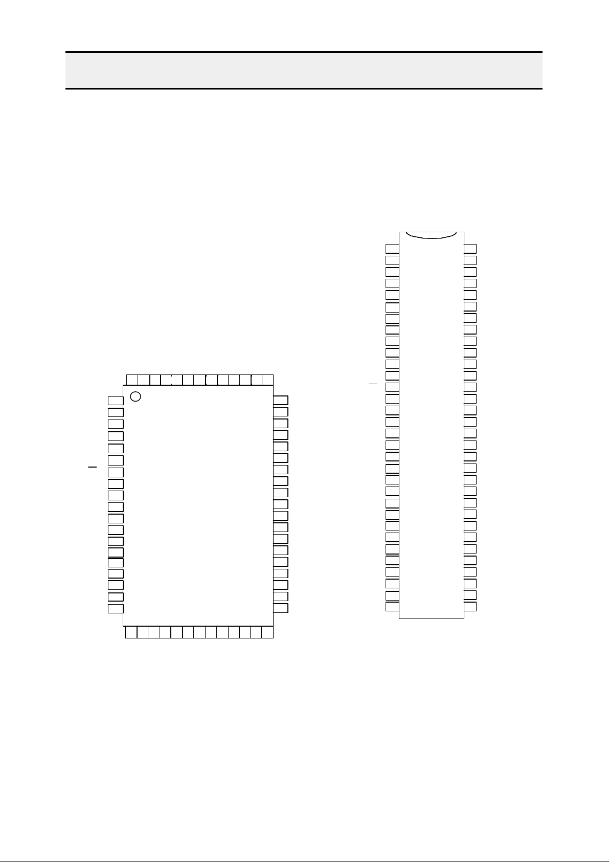
PIN CONFIGURATIONS
DD
P22 51 PD1
P23 50 PD0
P00 / INT0 TI0 49 PC3
P01 / INT1 TI1 48 PC2
P02 / INT2 TI2 47 PC1
P03 / INT3 46 PC0
P10 / SCK 45 AV
P11 / SI 44 AV
P12 / SO 43 PB3 / AD7
P13 / BUZ 42 PB2 / AD6
P30 41 PB1 / AD5
P31 40 PB0 / AD4
P32 39 PA3 / AD3
P33 38 PA2 / AD2
RESETB 37 PA1 / AD1
XI 36 PA0 / AD0
XO 35 P93
P40 34 P92
P41 33 P91
1
2
3
4
5
6
7
8
9
10
11
12
13
14
15
16
17
18
19
DMC42C4008
DD
SS
P80 1 64 V
P81 2 63 P63
P82 3 62 P62
P83 4 61 P61
P20 / CLO 5 60 P60
P21 6 59 PD3
P22 7 58 PD2
P23 8 57 PD1
P00 / INT0 / TI0 9 56 PD0
P01 / INT1 / TI1 10 55 PC3
P02 /INT2 / TI2 11 54 PC2
P03 / INT3 12 53 PC1
P10 / SCK 13 52 PC0
P11 / SI 14 51 AV
P12 / SO 15 50 AV
P13 / BUZ 16 49 PB3 / AD7
P30 17 48 PB2 / AD6
P31 18 47 PB1 / AD5
P32 19 46 PB0 / AD4
P33 20 45 PA3 / AD3
RESETB 21 44 PA2 / AD2
XI 22 43 PA1 / AD1
XO 23 42 PA0 / AD0
P40 24 41 P93
P41 25 40 P92
P42 26 39 P91
P43 27 38 P90
P50 28 37 P73
P51 29 36 P72
P52 30 35 P71
P53 31 34 P70
VSS 32 33 TEST
D
M
C
4
2
C
4
0
0
DD
DD
SS
SS
V
Page 2

2
4Bit Single Chip Microcontroller
FEATURE
Memory mapped I/O
8-bit A/D converter
- 8-bit successive approximate type
Program memory : 8192 x 10bits
- 8 channels
- Sample and hold
Data memory : 512 x 4bits
- Conversion time : 17.1 us at 4.19MHz
Instructions
Key scan
- Various bit manipulation
- 4, 6, 8 Pins Selectable : Port 4, 5
- 8-bit data operation
- Falling edge operation
- 7-bit relative branch
- 1 byte absolute call
56 I/O Ports
- CMOS Ports : 40
Instruction cycle times
- N-channel open drain Ports : 16
- Main ( XI = 4.19MHz )
- Direct LED drive
. 15.3 us ( XI/64 = 65.5KHz )
- Internal pull-up resistor (Mask option)
. 1.91 us ( XI/8 = 524.0KHz )
. 0.95 us ( XI/4 = 1.05MHz )
Power saving mode
- STOP : Main clock, CPU clock stop
4 Register Bank
- STBY : Only CPU clock stop
Main clock operation
General register : 8 x 4-bit respectively
Package : 64 QFP, 64 SDIP
Accumulator
- Bit Accumulator (CY), 4 bit Accumulator (A),
8 bit Accumulator (XA)
Multiple vectored interrupt source
APPLICATION
- Internal interrupt : 7
VTR, Audio, Telephone, Printer, Refrigerator
Watch timer
Fan Heater, Washing Machine
- fast mode : 3.91 msec
- normal mode : 0.5 sec
- buzzer output : 1, 2, 4 KHz
Basic interval timer
- 8 kinds of period
- Used stabilization wait timer to wake up Stop mode
Three 8-bit timer / event counters
8-bit serial communication interface
- External / Internal clock selection
- Mode : Transmit ·Receive
Receive only
Clock continuous
- External interrupt : 4
Page 3
3
4Bit Single Chip Microcontroller
DMC42C4008
SO / P12
INT3/P03
PB0~PB3
Fx / 2
RESETB
TEST
AV
V
DD
P20 / CLO
V
SS
XI
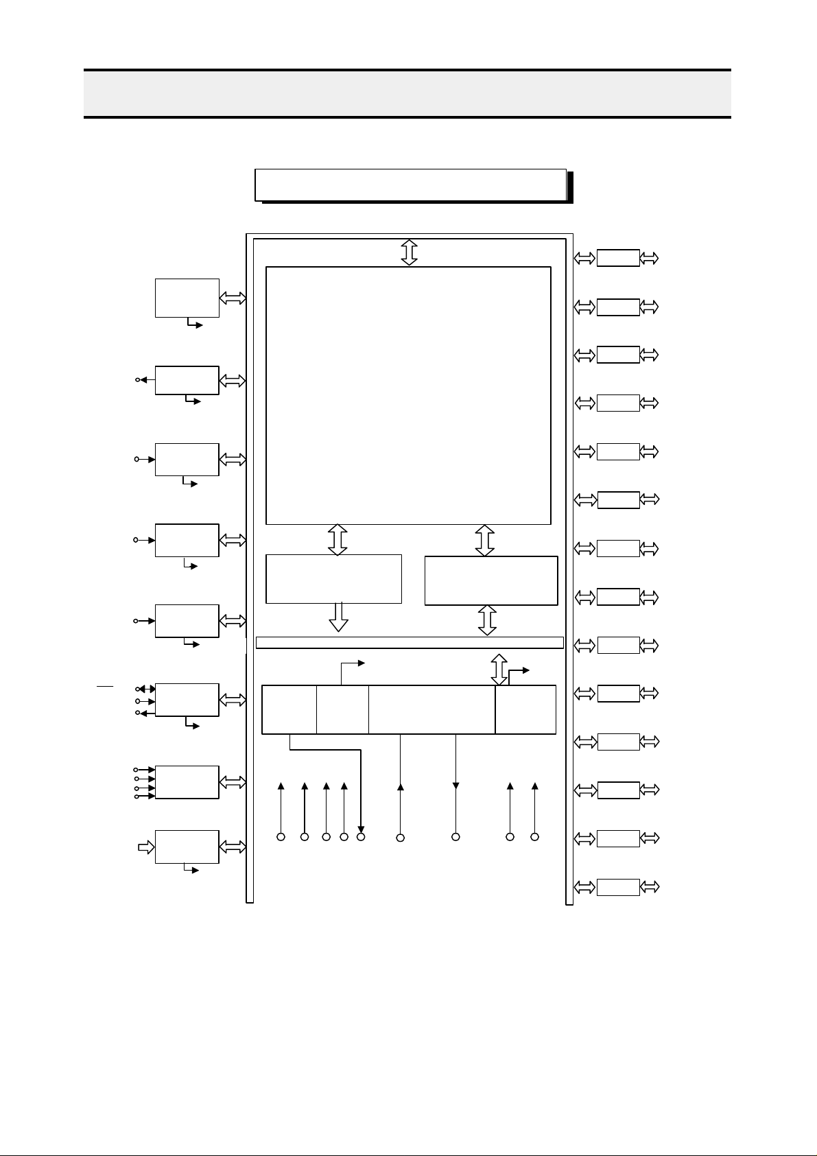
BLOCK DIAGRAM
BUZ/P13
TI0 / P00
TI1 / P01
TI2 / P02
SCK/P10
SI / P11
BASIC
INTERVAL
TIMER
WATCH
TIMER
TIMER/EVENT
COUNTER 0
TIMER/EVENT
COUNTER 1
TIMER/EVENT
COUNTER 2
SERIAL
INTERFACE
IRQBT
IRQWT
IRQTC 0
IRQTC 1
IRQTC 2
IRQS0
DMC42 CORE
PROGRAM MEMORY
(8192 X 10BITS)
CLOCK
OUTPUT
CONTRO
CLOCK
DIVIDER
DATA MEMORY
n
CLOCK
GENERATOR
(512 X 4BITS)
STOP/
IDLE
CONTROL
CPU
CLOCK
PORT0
PORT1
PORT2
PORT3
PORT4
PORT5
PORT6
PORT7
PORT8
PORT9
PORT
P00 ¡- P03
P10 ¡- P13
P20 ¡- P23
P30 ¡- P33
P40 ¡- P43
P50 ¡- P53
P60 ¡- P63
P70 ¡- P73
P80 ¡- P83
P90 ¡- P93
PA0 ¡- PA3
INT0/P00
INT1/P01
INT2/P02
PA0~PA3
,
INTERRUPT
CONTROL
8-BIT ADC
IRQAD
DDAVSS
PORT
PORT
PB0 ¡- PB3
PC0 ¡- PC3
XO
PORT
PD0 ¡- PD3
Page 4
4
4Bit Single Chip Microcontroller
DMC42C4008
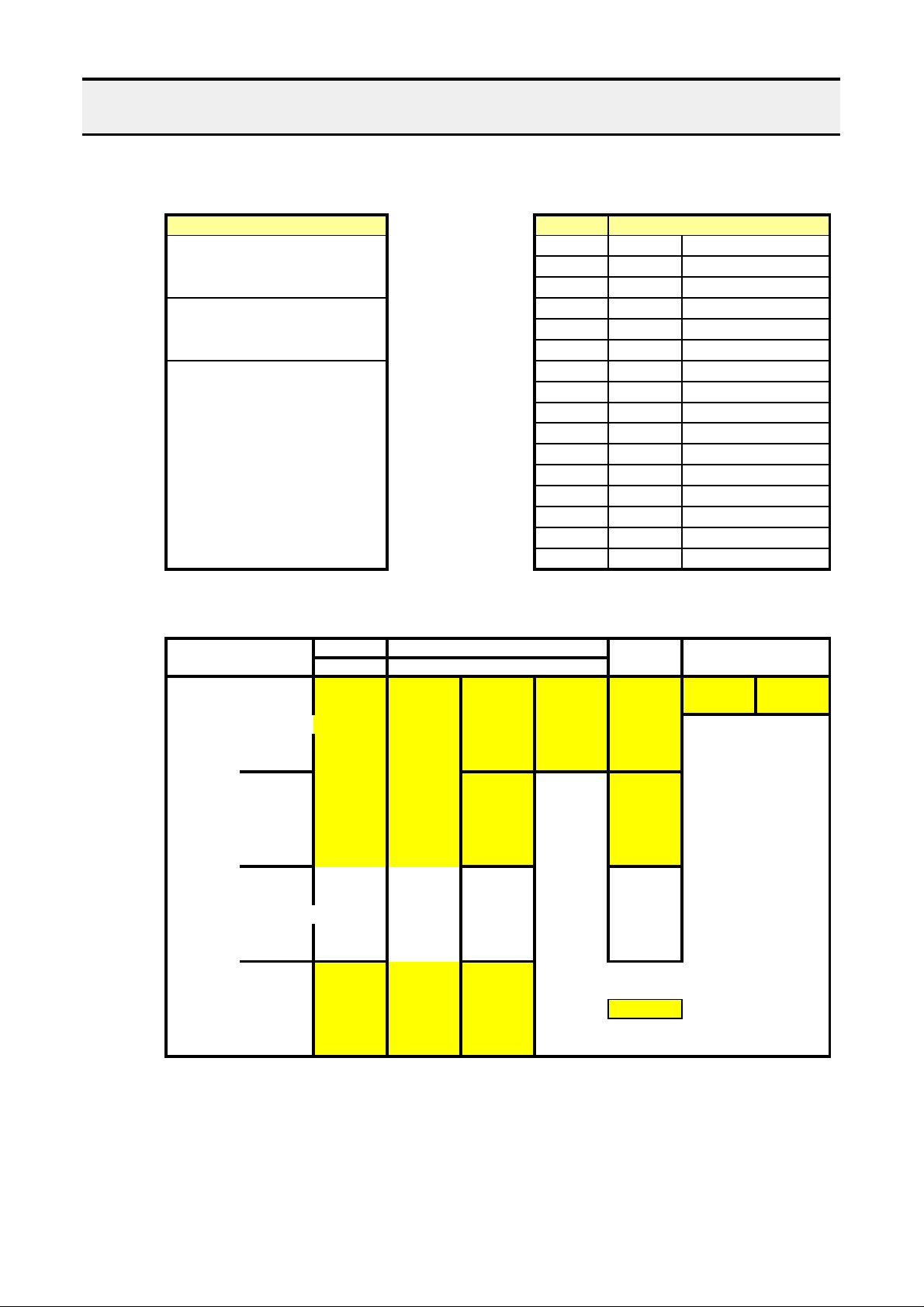
PROGRAM MEMORY (ROM)
VECTOR ADDRESS
CONTENTS Prioty INTERRUPT SUORCE
DATA MEMORY (RAM)
RB=0
RB=1
RB=2
RB=4
MP=0
SPS=0
(256 Byte)
MB=0
MB=0
MP=1
SPS=1
BANK 0
(1K)
MP=2
SPS=2
I/O
(256 Byte)
MEMORY
MP=3
0000H
VECTOR
ADDRESS AREA
001FH 0004H
0020H
ZERO-PAGE
CALL AREA
005FH 000AH
0060H 000CH
8K Byte
1FFFH 001EH
0000H
0002H
0006H
0008H
000EH
0010H
0012H
0014H
0016H
0018H
001AH
001CH
DIRECT INDIRECT STACK GENERAL
m @HL @DE @DL REGISTER
$00
PAGE0
(256 Byte)
0 RESET
1 IRQBT
2 IRQ0
3 IRQ1
4 IRQTC0
5 IRQTC1
6 IRQ2
7 IRQTC2
8 IRQ3
9 IRQS0
10 IRQAD
12 IRQWT
13 IRQKS
15 -
Reset Signal
Basic Interval Timer
External interrupt 0
External interrupt 1
Timer Event Counter 0
Timer Event Counter 1
External interrupt 2
Timer Event Counter 2
External interrupt 3
Serial I/O 0
8 bit ADC
Watch Timer
Key Scan
reserved
$FF
$00
PAGE1
$FF
$00
PAGE2
(256 Byte)
$FF
$00
PAGE3
$FF
; Usable
Page 5
5
4Bit Single Chip Microcontroller
DMC42C4008
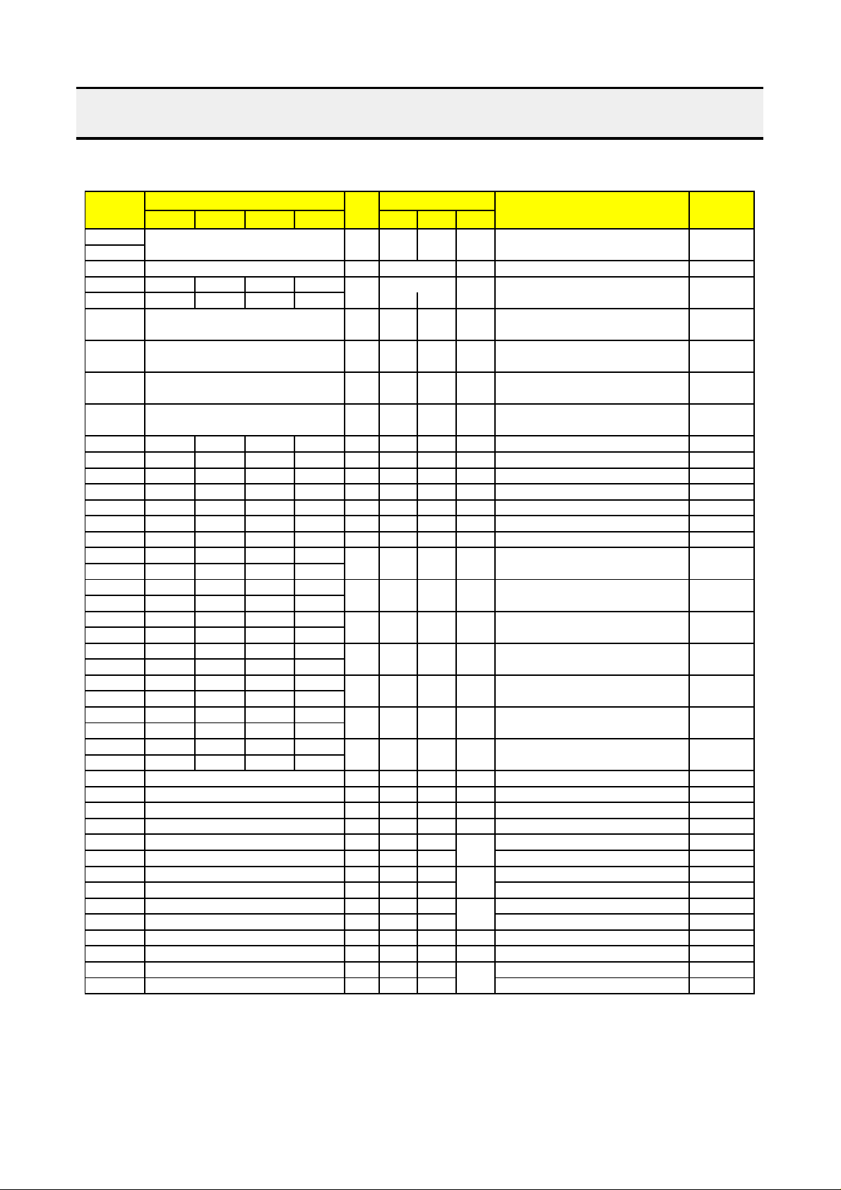
I/O ADDRESS MAP
ADDRESS Hardware Module Name R/W Addressing Unit REMARKS INITIAL
3ACH.3
b3 b2 b1 b0 1 bit 4 bit 8bit VALUE
318H Stack pointer low (SPL) R/W O Stack pointer low E
319H Stack pointer high (SPH) R/W O stack pointer high F
31AH SP3 SP2 SP1 SP0 R/W O Stack Page Select Low (SPSL) 0
31BH - - SP5 SP4 R/W O Stack Page Select High (SPSh) 0
31CH AC IS1 IS0 R/W O O O Psw low (PSWL) 0
31DH CY Z OV T Psw high (PSWH) 0
320H T/E counter mode register 0 W 320H.3 O Clock source select. counter 00
321H (TMOD0) start (ch0)
322H T/E counter register 0 R O readable count value (ch0) 00
323H (TMCNT0)
324H T/E reference register 0 W O count reference register (ch0) FF
325H (TMREF0)
326H T/E counter mode register 1 W 326H.3 O clock source select. counter start 00
327H (TMOD1) (ch1)
328H T/E counter register 1 R O readable count value (ch1) 00
329H (TMCNT1)
32AH T/E reference register 1 W O count reference register (ch1) FF
32BH (TMREF1)
32CH T/E counter mode register 2 W 32CH.3 O clock source select. counter 00
32DH (TMOD2) start (ch2)
32EH T/E counter register 2 R O readable count value (ch2) 00
32FH (TMCNT2)
330H T/E reference register 2 W O count reference register (ch2) FF
331H (TMREF2)
332H Basic Timer mode register(BMOD) R/W 332H.3 O clock select, Bit start 0
334H Basic interval timer count R O readable count register 00
335H register(BITCNT)
336H Watch timer mode register R/W 336H.3 O clock/buzzer select. bit3 00
337H (WMOD) readable
386H Adc8 mode register (ADCM8) R/W 386H.3 O analog input pin select. start & 00
387H low 4bit readable
388H Adc8 output latch (ADCOL8) R O 8bit conversion data 00
389H
3A0H Power control register O system clock select, idle, stop 00
(PCON) R/W mode
3A2H Operating mode register (SCMOD) R/W O main/sub system clock select 0
3A4H Clock output mode register W O cpu clock output select, clock 00
(CLOMD) out EN/DIS
3A8H Serial interface mode register0 W 3A8H.3 O receive/transmit mode. clock 00
3A9H (SIOM0) select
3AAH Serial interface buffer0 R/W serial shift register 0 XX
3ABH (SBUFF0)
3ACH Serial interface mode register1 W
3ADH (SIOM1) select
O receive/transmit mode, clock 00
Page 6
6
4Bit Single Chip Microcontroller
DMC42C4008
ADDRESS Hardware Module Name R/W Addressing Unit REMARKS INITIAL
b3 b2 b1 b0 1 bit 4 bit 8bit VALUE
3AEH Serial interface buffer1 R/W O serial shift register 1 00
3AFH (SBUFF1)
3B2H Power on flag (PONF) P/W 3B2H.0 O power on reset flag 0
3C2H IME R/W 3C2H.3 O Interrupt priorty select, IME flag. 00
3C3H IPSR3 IPSR2 IPSR1 IPSR0
3C4H External interrupt mode register0 W O external interrupt 0 edge 00
(IMOD0) detection
3C5H External interrupt mode register1 W O external interrupt 1 edge 00
(IMOD1) detection
3C6H External interrupt mode register2 W O external interrupt 2 edge 00
(IMOD2) detection
3C7H External interrupt mode register3 W O external interrupt 3 edge 00
(IMOD3) detection
3D8H IE2 IRQ2 IEBT IRQBT R/W O O Interrupt EN/IRQ flag 0
3D9H IEAD8 IRQAD8 IEWT IRQWT R/W O O Interrupt EN/IRQ flag 0
3DAH IES0 IRQS0 R/W O O Interrupt EN/IRQ flag 0
3DBH IETC1 IRQTC1 IETC0 IRQTC0 R/W O O Interrupt EN/IRQ flag 0
3DCH IE1 IRQ1 IE0 IRQ0 R/W O O Interrupt EN/IRQ flag 0
3DDH IETC2 IRQTC2 IES1 IRQS1 R/W O O Interrupt EN/IRQ flag 0
3DEH IE3 IRQ3 R/W O O Interrupt EN/IRQ flag 0
3E0H PW03 PW02 PW01 PW00 W O port 0, 1 mode register (PMGA) 00
3E1H PW13 PW12 PW11 PW10
3E2H PW23 PW22 PW21 PW20 W O port 2, 3 mode register (PMGB) 00
3E3H PW33 PW32 PW31 PW30
3E4H PW43 PW42 PW41 PW40 W O port 4, 5 mode register (PMGC) 00
3E5H PW53 PW52 PW51 PW50
3E6H PW63 PW62 PW61 PW60 W O port 6, 7 mode register (PMGD) 00
3E7H PW73 PW72 PW71 PW70
3E8H PW83 PW82 PW81 PW80 W O port 8, 9 mode register (PMGE) 00
3E9H PW93 PW92 PW91 PW90
3EAH PWA3 PWA2 PWA1 PWA0 W O port a, b mode register (PMGF) 00
3EBH PWB3 PWB2 PWB1 PWB0
3ECH PWC3 PWC2 PWC1 PWC0 W O port c, d mode register (PMGG) 00
3EDH PWD3 PWD2 PWD1 PWD0
3F0H PORT0 (R0) R/W O O R0 Port Data Register 0
3F1H PORT1 (R1) R/W O O R1 Port Data Register 0
3F2H PORT2 (R2) R/W O O R2 Port Data Register 0
3F3H PORT3 (R3) R/W O O R3 Port Data Register 0
3F4H PORT4 (R4) R/W O O O R4 Port Data Register 0
3F5H PORT5 (R5) R/W O O R5 Port Data Register 0
3F6H PORT6 (R6) R/W O O R6 Port Data Register 0
3F7H PORT7 (R7) R/W O O R7 Port Data Register 0
3F8H PORT8 (R8) R/W O O R8 Port Data Register 0
3F9H PORT9 (R9) R/W O O R9 Port Data Register 0
3FAH PORTA (RA) R/W O O RA Port Data Register 0
3FBH PORTB (RB) R/W O O RB Port Data Register 0
3FCH PORTC (RC) R/W O O O RC Port Data Register 0
3FDH PORTD (RD) R/W O O RD Port Data Register 0
Page 7

7
4Bit Single Chip Microcontroller
DMC42C4008
PIN DESCRIPTION
PIN
SHARED
I/O
FUNCTION
RESET
PORT
SYMBOL
PIN TYPE
P00 INT0/TI0
NOTE ) P4, P5, PC, PD : 8-bit operation possible
P01 INT1/TI1 I/O 4-BIT I/O PORT BPS
P02 INT2/TI2 PORT 0
P03 INT3
P10 SCK
P11 SI I/O 4-BIT I/O PORT BPS
P12 SO PORT 1
P13 BUZ
P20 CLO I/O 4-BIT I/O PORT BP
P21~ P23 - PORT 2
P3 - I/O 4-BIT I/O PORT. PORT3 BP
P4 - 4-BIT I/O PORT. PORT4 BD
P5 - 4-BIT I/O PORT. PORT5
P6 - 4-BIT I/O PORT. PORT6 BP-PDND
P7 - 4-BIT I/O PORT. PORT7 INPUT
P8 - 4-BIT I/O PORT. PORT8
P9 - 4-BIT I/O PORT. PORT9 BP
PA AD0~AD3 4-BIT I/O PORT. PORTA
PB AD4~AD7 4-BIT I/O PORT. PORTB
PC - 4-BIT I/O PORT. PORTC BD
PD - 4-BIT I/O PORT. PORTD
INT0/TI0 P00 I External interrupt input port
INT1/TI1 P01 rising/falling edge detection BP
INT2/TI2 P02 Event pulse input port for the
INT3 P03 timer/event counters
SCK P10 I/O Serial clock in/out port
SI P11 I Serial data input port BPS
SO P12 O Serial data output port
BUZ P13 O Buzzer output port
CLO P20 O Clock output port
Key scan P4-P5 I 4, 6, 8, bits Key scan input selectable BP
AD0~AD3 PA I Analog input for the 8-bit A/D converter
AD4~AD7 PB
XI, XO are the input and output, resp-
XI - ectively, of an inverting amplifier. The pins OSC1
XO can be configured for use as an on-chip
oscillator.
RESETB - I Reset input pin IP1
TEST - I Connect to VSS BP1
AVDD, AVSS - Power & ground for the A/D converter
VDD, VSS - Power & ground
Page 8

8
4Bit Single Chip Microcontroller
DMC42C4008
I/O CIRCUITS
NOTE) PUR : Pull-Up Resistor
M.O : Mask Option
VDDV
SS
VSSVDDV
DD
V
SS
V
D
DATA
V
SS
BP BPS
V
DD
OUTPU
DATA
INTERNAL
PUR
PUR
OUTPUT
DATA
BP-PDNDBD
Output
TR
Disable
OUTPUT
DATA
PUR
INTERNAL
Schmitt Trigger
PUR
OUTPU
INTERNA
Output
TR
Disable
INTERNA
Page 9

9
4Bit Single Chip Microcontroller
DMC42C4008
XI
XO
V
SS
V
SS
PAD
PAD
V
DD
PAD
V
DD
IP1 BP1
OSC1
P73/TEST(OTP
Page 10

10
4Bit Single Chip Microcontroller
DMC42C4008
ABSOLUTE MAXIMUM RATINGS
(TA = 0¡É to 70¡É, VDD = 5V ±10%, fX = 4.19MHz)
PARAMETER SYMBOL CONDITION RATING UNIT
Supply Voltage - -0.3 to +7.0 V
Input Voltage All I/O ports -0.3 to VDD+0.3 V
Output Voltage - -0.3 to VDD+0.3 V
Output Current High One I/O port active -15 mA
Output Current Low One I/O port active Peak Value +30
Operating Temperature - -40 to +85
Storage Temperature Tstg - -55 to +125
VDD
VI
VO
IOH
IOL
TA
All I/O ports active -30
- RMS Value +15
Total value for ports Peak Value +100 mA
P1, P2, P3, P8 RMS Value +60
Total value for ports Peak Value +100
P0, P4, P5, P6 RMS Value +60
¡É
¡É
* RMS values are calculated as peak value x Duty
* Exceeding beyond those listed values under "Absolute Maximum Ratings" may cause permanent damage
to the device.
Page 11

11
4Bit Single Chip Microcontroller
DMC42C4008
DC ELECTRICAL CHARACTERISTICS
SYMBOL
Main Clock (XI)
Main Clock (XI)
(IOL = 4mA)
(IOL
400uA)
(IOL
10mA)
(VSS = 0, VDD = 5V ±10%, TA = 25¡É, fX = 4.19MHz)
PARAMETER
High Level Port 0 ~ Port D 0.7VDD - VDD V
Input Voltage RESETB, XI 0.8VDD - VDD
Low Level Port 0 ~ Port D (Excepted TEST/R73) - - 0.3VDD V
Input Voltage RESETB, XI, TEST/R73 - - 0.2VDD
High Level All Ports Except Open 0.85VDD - -
Output Voltage Drain Ports 0.95VDD - - V
Low Level All Ports - - 0.5 V
Output Voltage - - 0.3
- - 60 mV
High Level All Pin Except XI, RESETB - - 3
Input Leakage (VIN = VDD) - 1.2 100 uA
Current
Low Level All Pin Except RESETB, P73/TEST - - -3
VIH
VIL
VOH
(Port 4,5,C,D) 0.99VDD - -
VOL
IIH
TEST LIMIT UNIT
CONDITION MIN. TYP. MAX.
(IOH = - 4mA)
(IOH = - 1mA)
(IOH = - 100uA)
=
=
Input Leakage (VIN = 0V) - -1.2 -200 uA
Current
Supply Current Dynamic - - 10
= 4.19MHz Idle - - 5
Dynamic - - 2
= 2MHz Idle - - 1
IIL
IDD1
IDD2
Mode VDD = 5V ±10%
Mode mA
Mode VDD = 3V ±10%
Mode
Page 12

12
4Bit Single Chip Microcontroller
DMC42C4008
DC ELECTRICAL CHARACTERISTICS
SYMBOL
Main Clock (XI)
(VSS = 0, VDD = 5V ±10%, TA = 25¡É, fX = 4.19MHz)
PARAMETER
Supply Current
Internal Pull-up All Ports - - 40
Resistor (M.O) VI or VO = 0V, VDD = 5V
Pull-up VI = 0V, VDD = 5V ±10% 20 - 60 Kohm
Resistor RESETB
Pull-down VI = 0V, VDD = 5V ±10% 10 - 30
Resistor TEST
NOTES ) :
(1) Main system clock oscillation stops.
IDD3
(1)
RPU
RL1
RL2
= 4.19MHz Mode VDD = 3V ±10% - 0.5 3
TEST LIMIT UNIT
CONDITION MIN. TYP. MAX.
Stop VDD = 5V ±10% - 1 5 uA
Page 13

13
4Bit Single Chip Microcontroller
DMC42C4008
AC ELECTRICAL CHARACTERISTICS
(TA = -40 to +85¡É, VDD = 2.7 to 6.0V)
t
CY
f
TI
t
TIH
t
TILtKCY
tKHt
KL
t
KSI
t
SIK
t
KSO
t
RSL
t
KCY
/2~50
t
KCY
/2~15
t
INTHtINTL
PARAMETER SYMBOL TEST CONDITION MIN. TYP. MAX. UNIT
Cycle Time 0.95 - 64 uS
TI Input Frequency 0 - 1 MHz
TI Input High, Low 0.48 - - uS
Level Width 1.8 - - uS
SCK Cycle Time Input 800 - - nS
SCK High, Low Level Width Input 400 - - nS
SI Set up Time to SCK High 100 - - nS
SI Hold Time to SCK High 400 - - nS
SCK to S0 Output Input - - 300 nS
Delay Time Output - - 250 nS
VDD = 4.5 to 6.0V
VDD = 2.7 to 3.3V
VDD = 4.5 to 6.0V
VDD = 2.7 to 3.3V
VDD = 4.5 to 6.0V
VDD = 2.7 to 3.3V
VDD = 4.5 to
VDD = 2.7 to
VDD = 4.5 to
VDD = 2.7 to
VDD = 4.5 to
3.8 - 64 uS
0 - 275 KHz
Output 950 - - nS
Input 3200 - - nS
Output 3800 - - nS
Output - - nS
Input 1600 - - nS
Output - - nS
VDD = 2.7 to
INT 0 ~ 4 Input Level
High, Low 5 - - uS
RESETB Low Level 5 - - uS
Input - - 1000 nS
Output - - 1000 nS
5 - - uS
Page 14

14
4Bit Single Chip Microcontroller
DMC42C4008
AC Timing Measurement Points (Except XI and XTI)
Measurement
0.8VD0.2VD0.8V
D
0.2V
D
Input Data
Output Data
VDD-
0.4V
VDD-
0.4V
0.8V
D
0.2V
D
0.8V
D
0.2V
D
0.8V
D
0.2V
D
0.2V
D
Clock Timing
XI
XTI
Timer Event Counter
TI0
Serial Transfer Timing
SCK
1/XI
tXL
tXH
1/XTI
tXTL
1/fTI
tTIL tTIH
tKC
tKL tKH
tSIK tKSI
tXT
SI
SO
Interrupt Input Timing
INT0~3
KS0~7
RESETB Input Timing
RESET
tINT tINT
tRS
Page 15

15
4Bit Single Chip Microcontroller
DMC42C4008
RAM DATA RETENTION CHARACTERISTICS ( in STOP Mode )
(TA = -40 to +85¡É)
Signal
PARAMETER SYMBOL TEST CONDITION MIN. TYP. MAX. UNIT
Data Retention
Supply Voltage
Data Retention
Supply Current
Release Signal Set
Time
Oscillation
Stabilization
NOTE 1) Depends on the setting of the basic interval timer mode register.
(refer to the table below)
BMOD2 BMOD1 BMOD0 Oscillation Stabilization
0 0 0
0 1 1
1 0 0
1 0 1
VDDDR
IDDDR
tSREL
tWAIT
2.0 - 6.0 V
VDDDR = 2.0V
When released by RESETB When released by interrupt
( fX = 4.19MHz )
220/fX (Approximately 250ms)
217/fX (Approximately 31.3ms)
215/fX (Approximately 7.82ms)
213/fX (Approximately 1.95ms)
- 0.1 10 uA
0 - - uS
- NOTE 1) - mS
217/fx
- mS
Page 16

16
4Bit Single Chip Microcontroller
DMC42C4008
RAM DATA RETENTION TIMING
When STOP mode is released by RESETB input
When STOP mode is released by interrupt signal
t
WAI
Stabilization Wait Time
t
WAI
Stabilization Wait Time
Internal Reset Operation
VDD
STOP instruction execution
RESET
STOP Mode
RAM Data retention
VDDDR
STOP Mode
Operation
tSREL
Operation
VDD
STOP instruction execution
Interrupt Signal
(Rising Edge)
RAM Data retention
VDDDR
Page 17

17
4Bit Single Chip Microcontroller
DMC42P4008
DESCRIPTION
PIN CONFIGURATION
DD
35
35
EPD4
P42
P43
P50
P51
P53
V
V
/OEX
P70
P71
P72
P73/TEST
P90
P52
DMC42P4008
The DMC42P4008 is a system evaluation LSI
having a built in One-Time Programming circuit.
A programming and verification for the internal
EPROM is achieved by using a general EPROM
programmer with an adapter socket.
The function of this device is exactly same as
the DMC42C4008 with programming of the internal
EPROM. The DMC42P4008 is the OTP version
of the DMC42C4008 with replacement of MASK
ROM to EPROM as an internal ROM.
P22
P23
P00/INT0/TI0
P01/INT1/TI1
P02/INT2/TI2
P03/INT3
P10/SCK
P11/SI
P12/SO
P13/BUZ
P30
P31
P32
P33
RESETB
XI
XO
EPA0/P40
EPA1/P41
64 63 62 61 59 58 57 56 55 54 53 52
1
2
EPA12
3
EPA13
4
CEX
5
6
EPA8
7
EPA9
8
EPA10
9
EPA11
10
EPD0
11
EPD1
12
13
EPD2
EPD3
14
15
16
17
18
19
60
DMC42P4008
P80
1
P81
2
P82
3
P83
4
EPD4
P20/CL0
P00/INT0/TI0
P01/INT1/TI1
P02/INT2/TI2
P03/INT3
P10/SCK
PD1
51
PD0
50
PC3
49
PC2
48
PC1
47
46
PC0
AV
DD
45
AV
SS
44
PB3/AD7
43
42
PB2/AD6
41
PB1/AD5
PB0/AD4
40
39
PA3/AD3
PA2/AD2
38
PA1/AD1
37
PA0/AD0
36
35
P93
35
P92
34
P91
33
P13/BUZ
P21
P22
P23
P11/SI
P12/SO
P30
P31
P32
P33
RESETB
35
P40
P41
P42
P43
P50
P51
35
P52
P53
V
5
6
7
8
9
EPA12
EPA13
10
CEX
11
12
EPA8
13
14
EPA9
EPA10
15
16
EPA11
35
EPD0
3517
EPD1
18
EPD2
19
20
EPD3
21
XI
22
XO
23
EPA0
24
25
EPA1
26
EPA2
27
EPA3
28
EPA4
EPA5
29
35
EPA6
3530
31
EPA7
SS
32
D
M
C
4
2
P
4
0
0
64
63
62
61
60
59
58
57
56
55
54
53
52
51
50
49
3548
47
46
45
44
43
42
41
40
39
38
37
36
3535
34
33
V
DD
P63
P62
P61
P60
PD3
PD2
PD1
PD0
PC3
PC2
PC1
PC0
AV
DD
AV
SS
PB3/AD7
35PB2/AD6
PB1/AD5
PB0/AD4
PA3/AD3
PA2/AD2
PA1/AD1
PA0/AD0
P93
P92
P91
P90
P73/TEST
P72
P71
35
P70
VPP/OEX
26 27 28 29 30 31 3220 21 22 23 2524
SS
PP
Page 18

18
4Bit Single Chip Microcontroller
DMC42P4008
DEVICE OPERATION
The operational modes of the DMC42P4008 are listed in Table 1.
PIN NAME
V
IL
VDDVILVIHVOLVOHVPPVDDIOL = 2.1mA
VILVILVILVILVPPVILVPPVIHDIND
D
VILV
V
PP
= 12.5±0.5V
IOH = -400uA
A single 5V power supply is required in the read mode.
All inputs are TTL levels except for VPP / OEX.
PINS
MODE
READ 5.0V
PROGRAM 6.0V
VERIFY 6.0V
PROGRAM INHIBIT 6.0V High Z
CEX VPP / OEX
TABLE 1. Operating Modes
EPROM MODE USER MODE
TEST
RESETB
TABLE 2. The modes of DMC42P4008
DC PROGRAMMING CHARACTERISTICS
MODE
VDD
OUTPU
IH
OUT
OUT
LIMIT UNIT
SYMBO
Input Low Voltage -0.1 0.8 V
Input High Voltage 2.0 V
Output Low Voltage during Verify - 0.45 V
Output High Voltage during Verify 2.4 - V
Quick-pulse Programming 12.5 13.0 V
Quick-pulse Programming 6.0 6.5 V
TEST CONDITIONPARAMETER
MIN. MAX.
Page 19

19
4Bit Single Chip Microcontroller
DMC42C/P4008
PACKAGE DIMENSION
[ UNIT : Millimeter ]
17.00 x 0.2
19.05
64 SDIP
64
1 32
57.80 x 0.2
1.778
0.45 x 0.1
1.00 x 0.1
33
3.30 x 0.3
5.08Max
0.51Min
0.25
0°~ 15°
+0.1
-0.05
Page 20

20
4Bit Single Chip Microcontroller
DMC42C/P4008
PACKAGE DIMENSION
[ UNIT : Millimeter ]
0.35±0.05
0.8±0.15
64 QFP
14.0±0.1
1.0TYP
20.0±0.1
23.9±0.25
3.00MAX
17.9±0.25
0.15±0.05
1.8±0.2
 Loading...