

Page 1
© 2000 Fairchild Semiconductor Corporation DS006381 www.fairchildsemi.com
August 1986
Revised March 2000
DM74LS90 Decade and Binary Counters
DM74LS90
Decade and Binary Counters
General Description
Each of these monolithic counters contains four masterslave flip-flops and additio nal ga ting to pr ovid e a di vid e-b ytwo counter and a three-stage binary counter for which the
count cycle length is divide-by-five for the DM74LS90.
All of these counters have a gated zero reset and the
DM74LS90 also has gated set-to-nine inputs for use in
BCD nine’s complement applications.
To use their maximum count length (decade or four bit
binary), the B input is connected to the Q
A
output. The
input count pulses are applied to input A and the outputs
are as described in the appropriate truth table. A symmetrical divide-by-ten count can be obtained from the
DM74LS90 counters by conne cting the Q
D
output to the A
input and applying the input count to the B input which
gives a divide-by-ten square wave at output Q
A
.
Features
■ Typical power dissipation 45 mW
■ Count frequency 42 MHz
Ordering Code:
Devices also availab le in Tape and Reel. Specify by appending th e s uffix let t er “X” to the ordering code.
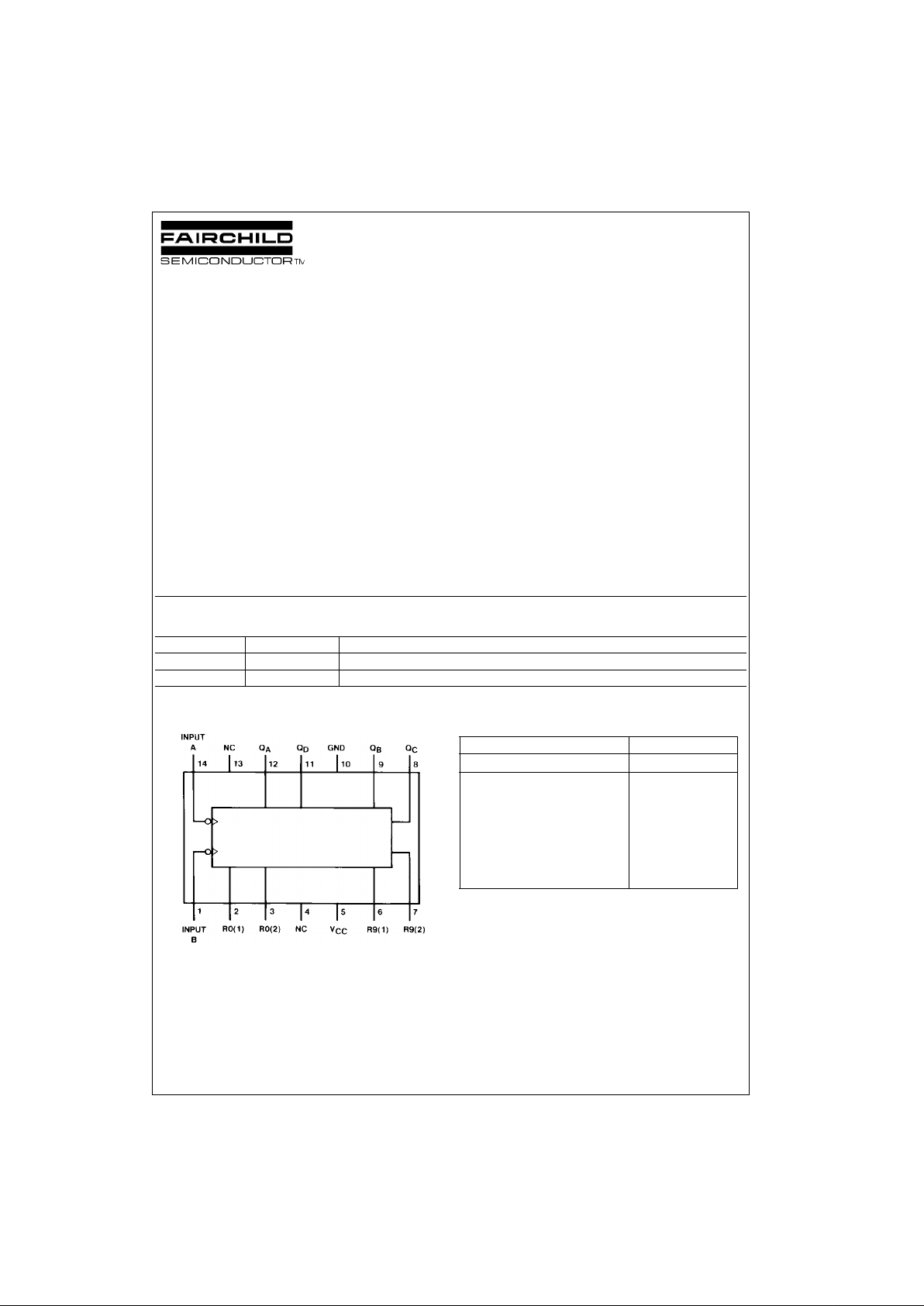
Connection Diagram Reset/Count Truth Table
Order Number Package Number Package Description
DM74LS90M M14A 14-Lead Small Outline Integrated Circuit (SOIC), JEDEC MS-120, 0.150 Narrow
DM74LS90N N14A 14-Lead Plastic Dual-In-Line Package (PDIP), JEDEC MS-001, 0.300 Wide
Reset Inputs Output
R0(1) R0(2) R9(1) R9(2) Q
DQCQBQA
H H L X LLLL
H H X L LLLL
XXHHHLLH
X L X L COUNT
L X L X COUNT
L X X L COUNT
X L L X COUNT
Page 2
www.fairchildsemi.com 2
DM74LS90
Function Tables
BCD Count Sequence (Note 1)
Bi-Quinary (5-2) (Note 2)
H = HIGH Level
L = LOW Level
X = Don’t Care
Note 1: Output Q
A
is connected to input B for BCD count.
Note 2: Output Q
D
is connected to input A for bi-quinary count.
Note 3: Output Q
A
is connected to input B.
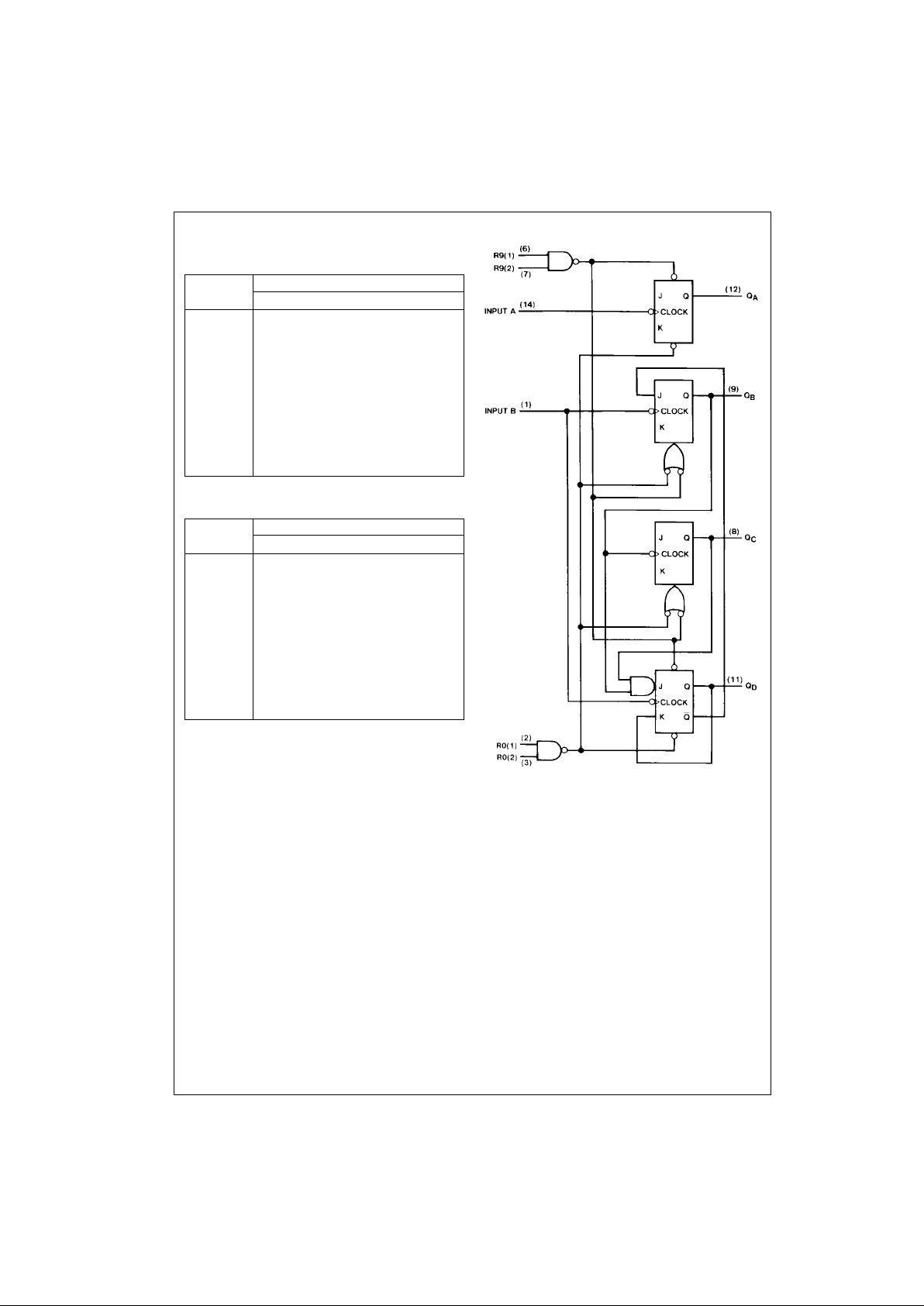
Logic Diagram
The J and K inputs sho wn without connec tion are for refere nce only and
are functionally at a high level.
Count Output
Q
D
Q
C
Q
B
Q
A
0 LLLL
1LLLH
2LLHL
3LLHH
4LHLL
5LHLH
6LHHL
7 LHHH
8 HLLL
9HLLH
Count Output
Q
A
Q
D
Q
C
Q
B
0 LLLL
1LLLH
2LLHL
3LLHH
4LHLL
5 HLLL
6HLLH
7HLHL
8HLHH
9HHLL
Page 3

3 www.fairchildsemi.com
DM74LS90
Absolute Maximum Ratings(Note 4)
Note 4: The “Absolute Maximum Ratings ” are those val ues beyond w hich
the safety of the device cannot be guaranteed. The device should not be
operated at thes e limits. The paramet ric values defined in the “Electrical
Characteristics” ta ble are not guaranteed at the absolute maxim um ratings.
The “Recommend ed O peratin g Cond itions” t able w ill defin e the condition s
for actual device operation.
Recommended Operating Conditions
Note 5: CL = 15 pF, RL = 2 kΩ, TA = 25°C and VCC = 5V.
Note 6: C
L
= 50 pF, RL = 2 kΩ, TA = 25°C and VCC = 5V.
Electrical Characteristics
over recommended operating free air temperature range (unless otherwise noted)
Note 7: All typicals are at VCC = 5V, TA = 25°C.
Supply Voltage 7V
Input Voltage (Reset) 7V
Input Voltage (A or B) 5.5V
Operating Free Air Temperature Range 0°C to +70°C
Storage Temperature Range −65°C to +150°C
Symbol Parameter Min Nom Max Units
V
CC
Supply Voltage 4.75 5 5.25 V
V
IH
HIGH Level Input Voltage 2 V
V
IL
LOW Level Input Voltage 0.8 V
I
OH
HIGH Level Output Current −0.4 mA
I
OL
LOW Level Output Current 8 mA
f
CLK
Clock Freq uency (Note 5) A to Q
A
032MHz
B to Q
B
016
f
CLK
Clock Freq uency (Note 6) A to Q
A
020MHz
B to Q
B
010
t
W
Pulse Width (Note 5) A 15
B30 ns
Reset 15
t
W
Pulse Width (Note 6) A 25
B50 ns
Reset 25
t
REL
Reset Release Time (Note 5) 25 ns
t
REL
Reset Release Time (Note 6) 35 ns
T
A
Free Air Operating Temperature 0 70 °C
Symbol Parameter Conditions Min
Typ
Max Units
(Note 7)
V
I
Input Clamp Voltage VCC = Min, II = −18 mA −1.5 V
V
OH
HIGH Level VCC = Min, IOH = Max
2.7 3.4 V
Output Voltage VIL = Max, VIH = Min
V
OL
LOW Level VCC = Min, IOL = Max
(Note 8)
VOutput Voltage VIL = Max, VIH = Min 0.35 0.5
IOL = 4 mA, VCC = Min 0.25 0.4
I
I
Input Current @ Max VCC = Max, VI = 7V Reset 0.1
mAInput Voltage VCC = Max A 0.2
VI = 5.5V B 0.4
I
IH
HIGH Level VCC = Max, VI = 2.7V Reset 20
µAInput Current A 40
B80
I
IL
LOW Level VCC = Max, VI = 0.4V Reset −0.4
mAInput Current A −2.4
B −3.2
I
OS
Short Circuit Output Current VCC = Max (Note 9) −20 −100 mA
I
CC
Supply Current VCC = Max (Note 7) 9 15 mA
Page 4

www.fairchildsemi.com 4
DM74LS90
Electrical Characteristics (Continued)
Note 8: QA outputs are tested at IOL = Max plus the limit value of IIL for the B input. This permits driving the B input wh ile maintaining full fan-o ut ca pability.
Note 9: Not more than one output should be shorted at a time, and the duration should not exceed one second.
Note 10: I
CC
is measured with all outputs open, both RO inputs grounded follow ing momentary conn ec t ion to 4.5V and all other in puts grounded.
Switching Characteristics at V
CC
= 5V and TA = 25°C
From (Input)
RL = 2 kΩ
Symbol Parameter
To (Output)
CL = 15 pF CL = 50 pF Units
Min Max Min Max
f
MAX
Maximum Clock A to Q
A
32 20
MHz
Frequency B to Q
B
16 10
t
PLH
Propagation Delay Time
A to Q
A
16 20 ns
LOW-to-HIGH Level Output
t
PHL
Propagation Delay Time
A to Q
A
18 24 ns
HIGH-to-LOW Level Output
t
PLH
Propagation Delay Time
A to Q
D
48 52 ns
LOW-to-HIGH Level Output
t
PHL
Propagation Delay Time
A to Q
D
50 60 ns
HIGH-to-LOW Level Output
t
PLH
Propagation Delay Time
B to Q
B
16 23 ns
LOW-to-HIGH Level Output
t
PHL
Propagation Delay Time
B to Q
B
21 30 ns
HIGH-to-LOW Level Output
t
PLH
Propagation Delay Time
B to Q
C
32 37 ns
LOW-to-HIGH Level Output
t
PHL
Propagation Delay Time
B to Q
C
35 44 ns
HIGH-to-LOW Level Output
t
PLH
Propagation Delay Time
B to Q
D
32 36 ns
LOW-to-HIGH Level Output
t
PHL
Propagation Delay Time
B to Q
D
35 44 ns
HIGH-to-LOW Level Output
t
PLH
Propagation Delay Time
SET-9 to QA, Q
D
30 35 ns
LOW-to-HIGH Level Output
t
PHL
Propagation Delay Time
SET-9 to QB, Q
C
40 48 ns
HIGH-to-LOW Level Output
t
PHL
Propagation Delay Time
SET-0 to Any Q 40 52 ns
HIGH-to-LOW Level Output
Page 5

5 www.fairchildsemi.com
DM74LS90
Physical Dimensions inches (millimeters) unless otherwise noted
14-Lead Small Outline Integrated Circuit (SOIC), JEDEC MS-120, 0.150 Narrow
Package Number M14A
Page 6

www.fairchildsemi.com 6
DM74LS90 Decade and Binary Counters
Physical Dimensions inches (millimeters) unless otherwise noted (Continued)
14-Lead Plastic Dual-In-Line Package (PDIP), JEDEC MS-001, 0.300 Wide
Package Number N14A
Fairchild does not assume any responsibility for use of any circuitry described, no circuit pate nt licenses are implied and
Fairchild reserves the right at any time without notice to change said circuitry and specifications.
LIFE SUPPORT POLICY
FAIRCHILD’S PRODUCTS ARE NOT AUTHORIZED FOR USE AS CRITICAL COMPONENTS IN LIFE SUPPORT
DEVICES OR SYSTEMS WITHOUT THE EXPRESS WRITTEN APPROVAL OF THE PRESIDENT OF FAIRCHILD
SEMICONDUCTOR CORPORATION. As used herein:
1. Life support devices or systems are devices or syste ms
which, (a) are intended for surgical implant into the
body, or (b) support or sustain life, and (c) whose failure
to perform when properly used in accordance with
instructions for use provided in the labeling, can be reasonably expected to result in a significant inju ry to the
user.
2. A critical component in any compon ent of a lif e supp ort
device or system whose failu re to perform can be reasonably expected to ca use the fa i lure of the life su pp ort
device or system, or to affect its safety or effectiveness.
www.fairchildsemi.com
 Loading...