

Page 1
DM74LS47
BCD to 7-Segment Decoder/Driver with
Open-Collector Outputs
DM74LS47 BCD to 7-Segment Decoder/Driver with Open-Collector Outputs
October 1988
Revised March 2000
General Description
The DM74LS47 accepts four lines of BCD (8421) input
data, generates their com plements interna lly and decodes
the data with seven AND/OR gates havin g open-collector
outputs to drive indica tor segm ents dir ectly. Each segment
output is guaranteed to sink 24 mA in the ON (LOW) state
and withstand 15V in the OF F (HIGH) state with a maximum leakage current of 250 µA. Auxilia ry inputs provided
blanking, lamp test and cascadable zero-suppression functions.
Features
■ Open-collector outputs
■ Drive indicator segments directly
■ Cascadable zero-suppression capability
■ Lamp test input
Ordering Code:
Order Number Package Number Package Description
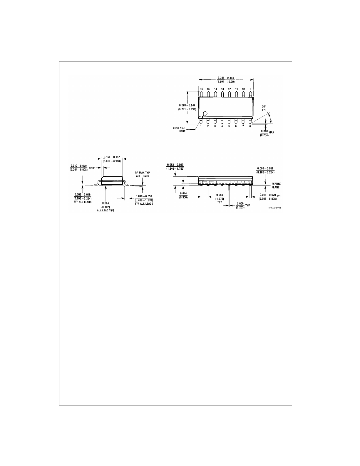
DM74LS47M M16A 16-Lead Small Outline Integrated Circuit (SOIC), JEDEC MS-012, 0.150 Narrow
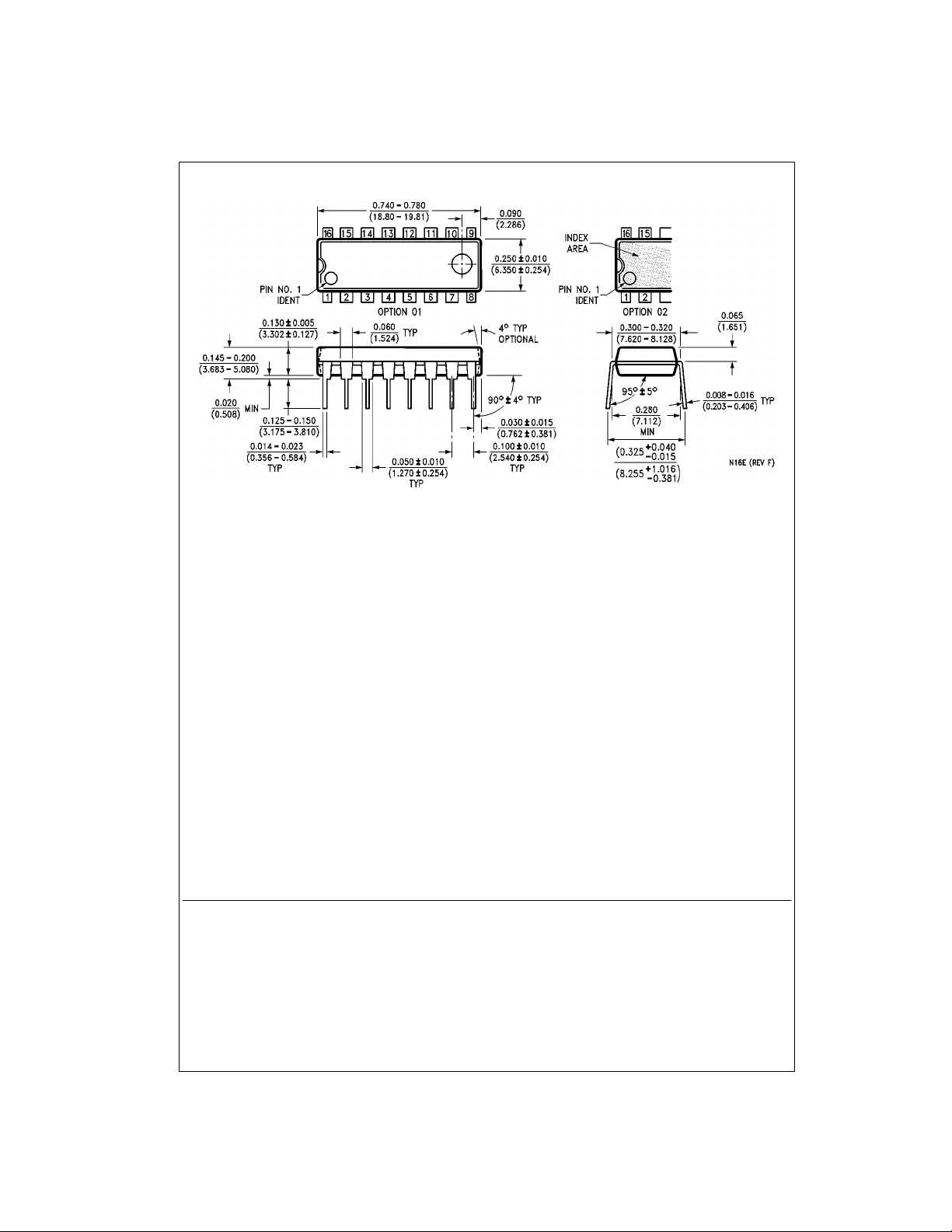
DM74LS47N N16E 16-Lead Plastic Dual-In-Line Package (PDIP), JEDEC MS-001, 0.300 Wide
Devices also availab le in Tape and Reel. Specify by appending th e s uffix let t er “X” to the ordering cod e.
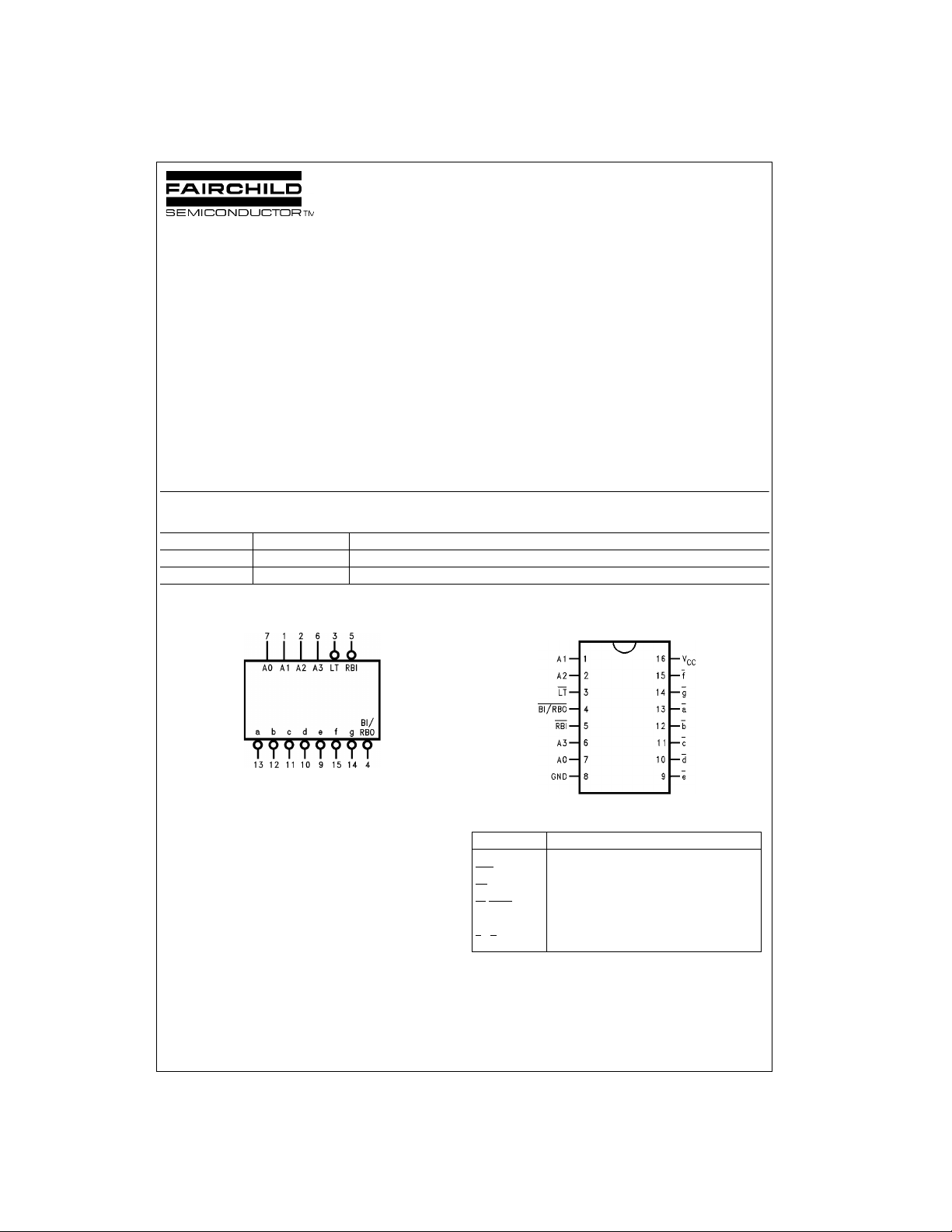
Logic Symbol
VCC = Pin 16
GND = Pin 8
Connection Diagram
Pin Descriptions
Pin Names Description
A0–A3 BCD Inputs
RBI
LT
/RBO Blanking Input (Active LOW) or
BI
–g Segment Outputs (Active LOW) (Note 1)
a
Note 1: OC—Open Collector
Ripple Blanking Input (Active LOW)
Lamp Test Input (Active LOW)
Ripple Blanking Output (Active LOW)
© 2000 Fairchild Semiconductor Corporation DS009817 www.fairchildsemi.com
Page 2
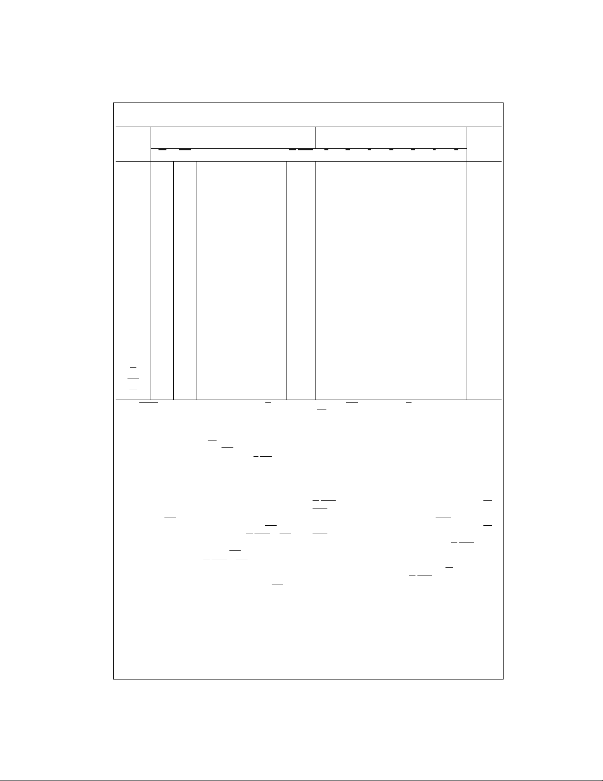
Truth Table
Decimal
or Note
Function
DM74LS47
LT
RBI A3 A2 A1 A0 BI/RBO a b c d e f g
0 HHLLLL H LLLLLLH(Note 2)
1 H X L L L H H H L L H H H H (Note 2)
2HXLLHLHLLHLLHL
3 HXLLHHHLLLLHHL
4HXLHLLHHLLHHLL
5 HXLHLHHLHLLHLL
6 HXLHHL H HHLLLLL
7 HXLHHHHLLLHHHH
8 HXHL LL H LLLLLLL
9 HXHL LH H LLLHHLL
10 H X H L H L H H H H L L H L
11 HXH LHH H HHLLHHL
12 H X H H L L H H L H H H L L
13 HXHHLHHLHHLHLL
14 HXHHHL H HHHLLLL
15 H XH HH H H HHHHHHH
BI
RBI
LT
Note 2: BI/RBO is wire-AN D logic serving as blanking input (BI) and/or ripple-b lanking output (RBO). The blanking out (BI) must be open or held at a HIGH
level when output fun ctions 0 through 15 ar e desired, and ripple-bl anking input (RBI
desired. X = input may be HIGH or LOW.
Note 3: When a LOW level is applied to the blanking input (forced condition) all segment outputs go to a HIGH level regardless of the state of any other input
condition.
Note 4: When ripple-b lanking input (RB I
HIGH level and the ripple-blanking output (RBO
Note 5: When the blanking input/ripple-blanking output (BI
outputs go to a LOW level.
XXXXXX L HHHHHHH(Note 3)
H L L L L L L HHHHHHH(Note 4)
LXXXXX H LLLLLLL(Note 5)
Inputs Outputs
) must be open or at a HIGH lev el if blanking or a decima l 0 is not
) and inputs A0, A1, A2 a nd A3 are LOW le vel, w ith t he l amp tes t i nput at HIGH lev el, all s egm ent out put s go to a
) goes to a LOW level (re sp onse condition).
/RBO) is OPEN or hel d at a HIG H lev el, and a LOW level is applied to lamp test input , all seg m ent
Functional Description
The DM74LS47 decodes the input data in the pattern indicated in the Truth Table and the segment identification
illustration. If the input data is decimal zero, a LOW signal
applied to the RBI
digit display. For example, by grounding the RBI
highest order deco der an d co nne cting i ts BI
the next lowest order decoder, etc., leading zeros will be
suppressed. Similarly, by grounding RBI
decoder and connecting its BI
est order decoder, etc., trailing zeros will be suppressed.
Leading and trailing zeros can be suppressed simultaneously by using external gates, i.e.: by driving RBI
www.fairchildsemi.com 2
blanks the display and causes a multi-
of the
/RBO to RBI of
of the lowest order
/RBO to RBI of the next high-
of a
intermediate decode r from an OR gate whose inputs are
BI
/RBO of the next highest and lowest ord er decoders. BI/
RBO also serves as an unconditio nal blanking input. The
internal NAND gate tha t generates the RBO
signal has a
resistive pull-up, as oppose d to a totem pole, and thu s BI/
RBO can be forced LOW by exte rnal means, usin g wiredcollector logic. A LOW signal thus app lied to BI
/RBO turns
off all segment outputs. This b lanking f eature can be used
to control display inten sity by vary ing the d uty cycle o f the
blanking signal. A LOW signal applied to LT
segment outputs, provided that BI
/RBO is not forced LOW.
turns on all
Page 3
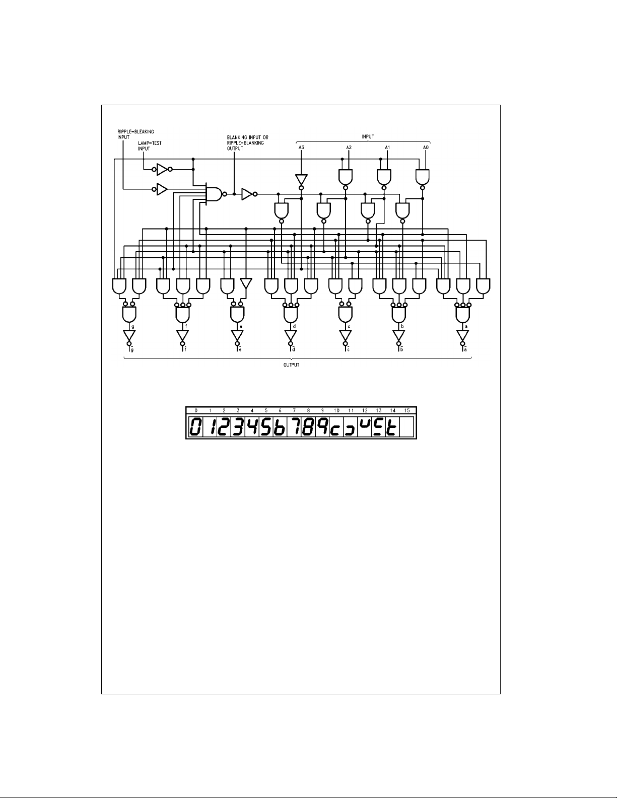
Logic Diagram
DM74LS47
Numerical Designations—Resultant Displays
3 www.fairchildsemi.com
Page 4
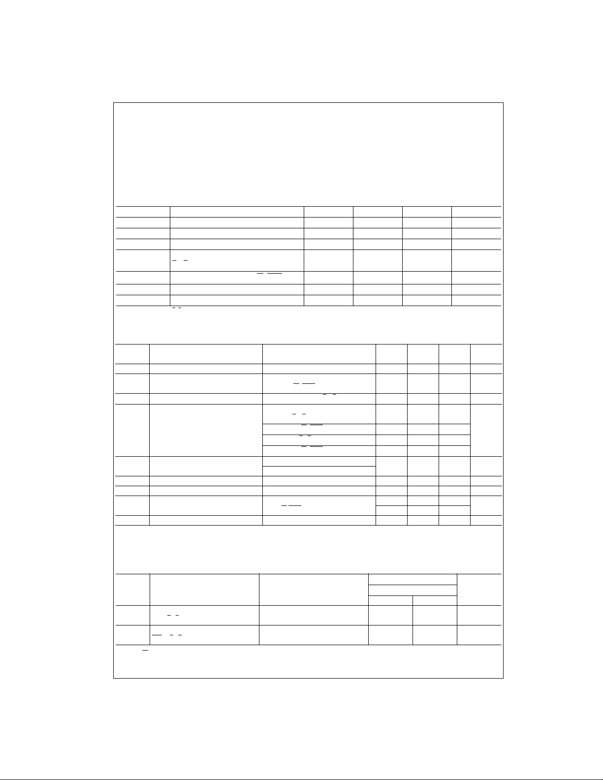
Absolute Maximum Ratings(Note 6)
Supply Voltage 7V
Input Voltage 7V
Operating Free Air Temperature Range 0°C to +70°C
DM74LS47
Storage Temperature Range −65°C to +150°C
Note 6: The “Absolute Maximum Ratin gs” are those v alues beyon d which
the safety of the dev ice cannot be guaranteed. T he device sh ould not be
operated at these limits. The parametric values defined in the Electrical
Characteristics tables are not guaranteed at the absolute maximum ratings.
The “Recommend ed O peratin g Cond itions” t able w ill defin e the c ondit ions
for actual device operation.
Recommended Operating Conditions
Symbol Parameter Min Nom Max Units
V
CC
V
IH
V
IL
HIGH Level Output Current
I
OH
I
OH
I
OL
T
A
Note 7: OFF-State at a–g.
Supply Voltage 4.75 5 5. 25 V
HIGH Level Input Voltage 2 V
LOW Level In put Voltage 0.8 V
− g @ 15V = VOH (Note 7)
a
−250 µA
HIGH Level Output Current BI /RBO −50 µA
LOW Level Ou tput Current 24 mA
Free Air Operating Temperature 0 70 °C
Electrical Characteristics
Over recommended operating free air temperature range (unless otherwise noted)
Symbol Parameter Conditions Min
V
I
V
OH
I
OFF
V
OL
I
I
I
IH
I
IL
I
OS
I
CC
Note 8: All typicals are at VCC = 5V, TA = 25°C.
Note 9: Not more than one output should be shorted at a time, and the duration should not exceed one second.
Input Clamp Voltage VCC = Min, II = −18 mA −1.5 V
HIGH Level VCC = Min, IOH = Max,
Output Voltage VIL = Max, BI /RBO
Output HIGH Current Segment Outputs VCC = 5.5V, VO = 15V a − g 250 µA
LOW Level VCC = Min, IOL = Max,
Output Voltage VIH = Min, a − g
IOL = 3.2 mA, BI /RBO 0.5 V
IOL = 12 mA, a –g 0.25 0.4
IOL = 1.6 mA, BI /RBO 0.4
Input Current @ Max VCC = Max, VI = 7V
Input Voltage VCC = Max, VI = 10V
HIGH Level Input Current VCC = Max, VI = 2.7V 20 µA
LOW Level Input Current VCC = Max, VI = 0.4V −0.4 mA
Short Circuit VCC = Max (Note 9),
Output Current IOS at BI/RBO −0.3 −2.0
Supply Current VCC = Max 13 mA
2.7 3.4 V
Typ
(Note 8)
0.35 0.5
Max Units
100 µA
mA
Switching Characteristics
at VCC = +5.0V, TA = +25°C
Symbol Parameter Conditions CL = 15 pF Units
t
PLH
t
PHL
t
PLH
t
PHL
Note 10: LT = HIGH, A0–A3 = LOW
Propagation Delay 100
An to a –g 100
Propagation Delay 100
RBI to a –g (Note 10) 100
www.fairchildsemi.com 4
RL = 665Ω
Min Max
ns
ns
Page 5
Physical Dimensions inches (millimeters) unless otherwise noted
DM74LS47
16-Lead Small Outline Integrated Circuit (SOIC), JEDEC MS-012, 0.150 Narrow
Package Number M16A
5 www.fairchildsemi.com
Page 6
Physical Dimensions inches (millimeters) unless otherwise noted (Continued)
16-Lead Plastic Dual-In-Line Package (PDIP), JEDEC MS-001, 0.300 Wide
Package Number N16E
DM74LS47 BCD to 7-Segment Decoder/Driver with Open-Collector Outputs
Fairchild does not assume any responsibility for us e of any circuitry described, no circuit patent licenses are implied and
Fairchild reserves the right at any time without notice to change said circuitry and specifications.
LIFE SUPPORT POLICY
FAIRCHILD’S PRODUCTS ARE NOT AUTHORIZED FOR USE AS CRITICAL COMPONENTS IN LIFE SUPPORT
DEVICES OR SYSTEMS WITHOUT THE EXPRESS WRITTEN APPROVAL OF THE PRESIDENT OF FAIRCHILD
SEMICONDUCTOR CORPORATION. As used herein:
1. Life support devices o r syste ms are devices or syste ms
which, (a) are intended for surgical implant into the
body, or (b) support or sustain life, and (c) whose failure
to perform when properly used in accordance with
instructions for use provided in the labeling, can be reasonably expected to result in a significan t injury to the
user.
2. A critical compon ent in any compon ent of a lif e supp ort
device or system whose failu re to perform can be reasonably expected to ca use the fa i lure of the li fe su pp ort
device or system, or to affect its safety or effectiveness.
www.fairchildsemi.com
www.fairchildsemi.com 6
 Loading...