

Datasheet DM74LS393N, DM74LS393MX, DM74LS393M, DM74LS393CW Datasheet (Fairchild Semiconductor)
Page 1
© 2000 Fairchild Semiconductor Corporation DS006434 www.fairchildsemi.com
August 1986
Revised March 2000
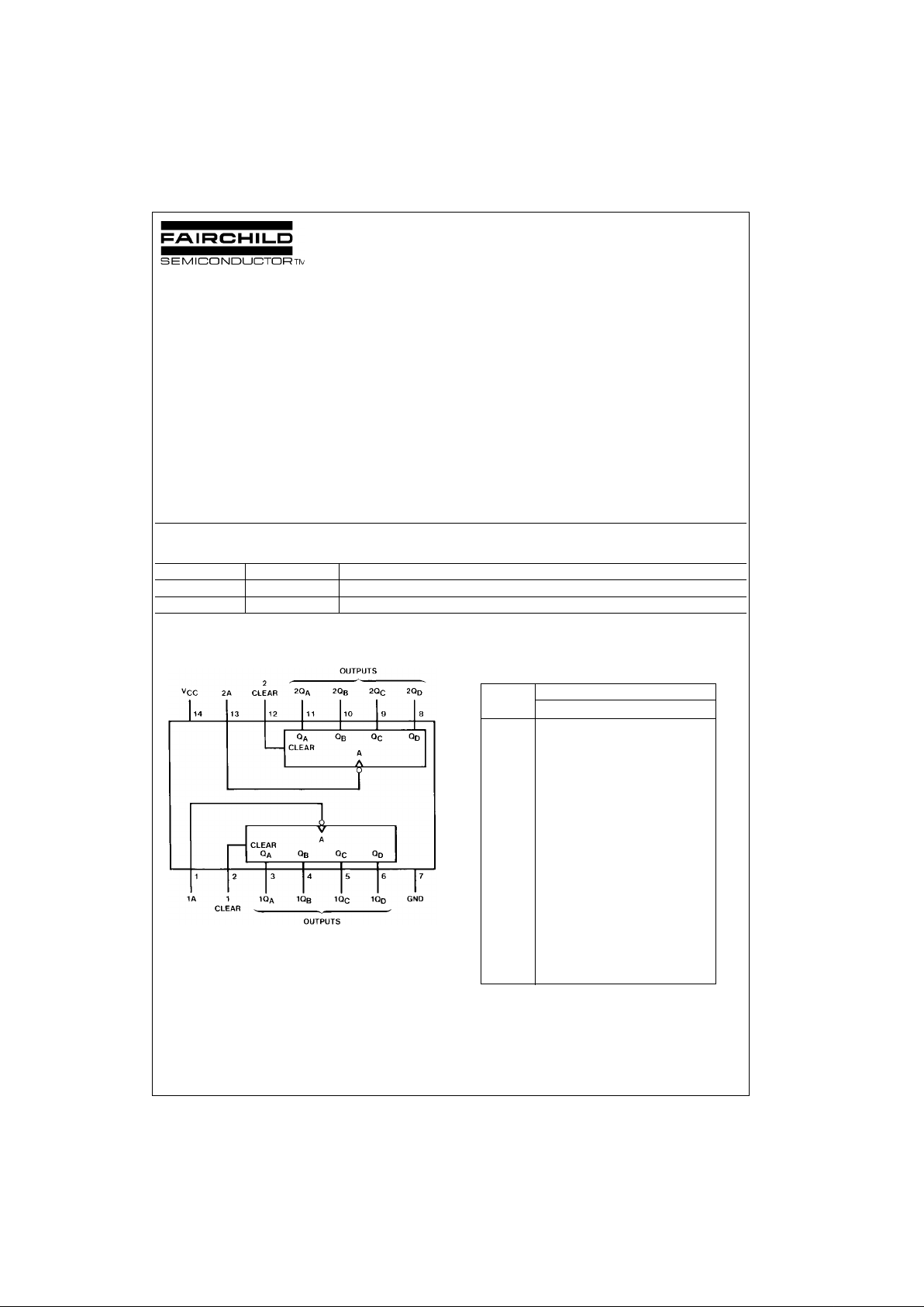
DM74LS393 Dual 4-Bit Binary Counter
DM74LS393
Dual 4-Bit Binary Counter
General Description
Each of these monolithic circuits contains eight masterslave flip-flops and additional gating to implement two individual four-bit counters in a single package. The
DM74LS393 comprises two independent four-bit binary
counters each having a clear and a clock input. N-bit binary
counters can be implemented with each package providing
the capability of divide-by-256. The DM74LS393 has parallel output s fro m ea c h c ount e r st ag e so th a t an y subm ul t ip l e
of the input count frequency is available for system -timing
signals.
Features
■ Dual version of the popular DM74LS93
■ DM74LS393 dual 4-bit binary counter with individual
clocks
■ Direct clear for each 4-bit counter
■ Dual 4-bit versions can significantly improve system
densities by reducing counter package count by 50%
■ Typical maximum count frequency 35 MHz
■ Buffered outputs reduce possibility of collector commu-
tation
Ordering Code:
Devices also availab le in Tape and Reel. Specify by appending th e s uffix let t er “X” to the ordering code.
Connection Diagram Function Table
Counter Sequence (Each Counter)
H = HIGH Logic Level
L = LOW Logic Level
Order Number Package Number Package Description
DM74LS393M M14A 14-Lead Small Outline Integrated Circuit (SOIC), JEDEC MS-120, 0.150 Narrow
DM74LS373N N14A 14-Lead Plastic Dual-In-Line Package (PDIP), JEDEC MS-001, 0.300 Wide
Count
Outputs
Q
D
Q
C
Q
B
Q
A
0 LLLL
1 LLLH
2LLHL
3LLHH
4LHLL
5LHLH
6LHHL
7 LHHH
8 HLLL
9HLLH
10HLHL
11 H L H H
12 H H L L
13 H H L H
14 HHHL
15 HHHH
Page 2
www.fairchildsemi.com 2
DM74LS393
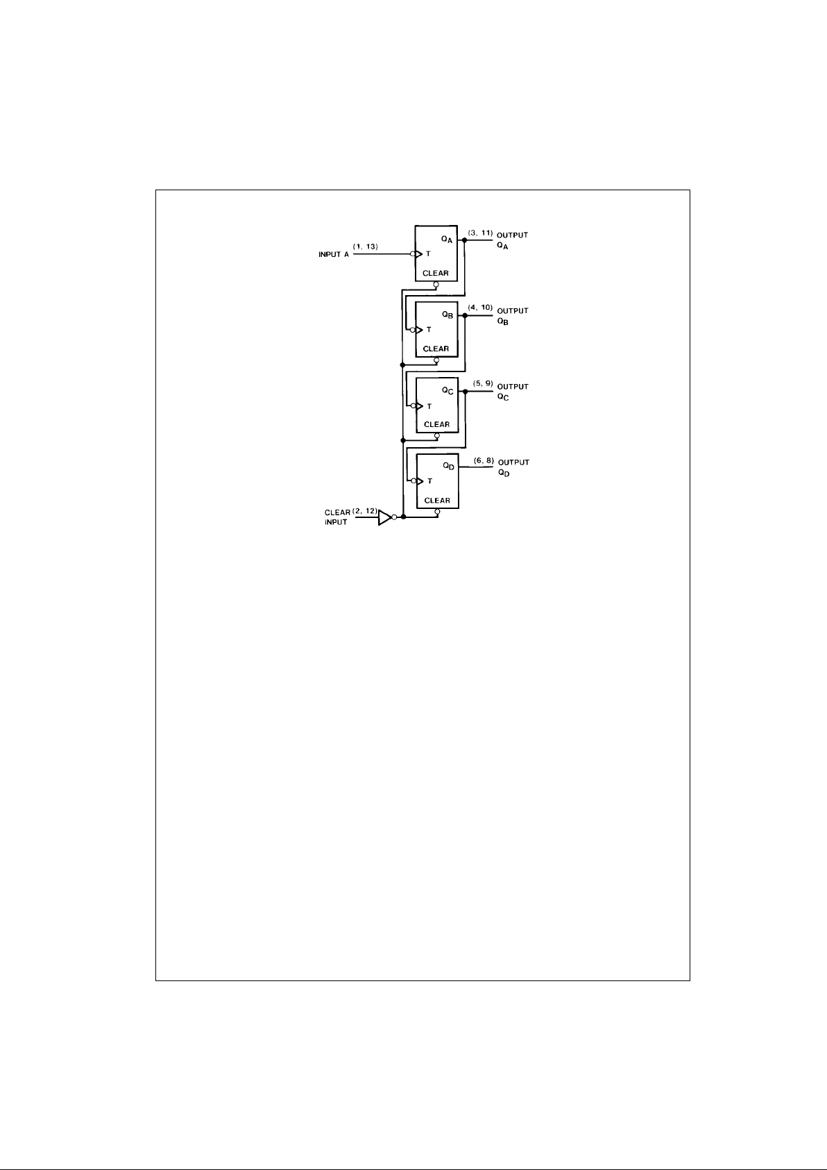
Logic Diagram
Page 3

3 www.fairchildsemi.com
DM74LS393
Absolute Maximum Ratings(Note 1)
Note 1: The “Absolute Maximum Ratings ” are those val ues beyond w hich
the safety of the device cannot be guaranteed. The device should not be
operated at these limits. The parametric values defined in the Electrical
Characteristics tables are not guaranteed at the absolute maximum ratings.
The “Recommend ed O peratin g Cond itions” t able w ill defin e the condition s
for actual device operation.
Recommended Operating Conditions
Note 2: CL = 15 pF, RL = 2 kΩ, TA = 25°C and VCC = 5V.
Note 3: C
L
= 50 pF, RL = 2 kΩ, TA = 25°C and VCC = 5V.
Note 4: The symbol (↓) indicates that the fa lling edge of the clear pulse is used for reference.
Note 5: T
A
= 25°C, and VCC = 5V.
Electrical Characteristics
over recommended operating free air temperature range (unless otherwise noted)
Note 6: All typicals are at VCC = 5V, TA = 25°C.
Note 7: Not more than one output should be shorted at a time, and the duration should not exceed one second.
Note 8: I
CC
is measured with all out puts open, both CLEA R inputs grounded follow ing momentary conne c t ion to 4.5V, and all other inputs grounded.
Supply Voltage 7V
Input Voltage
Clear 7V
A5.5V
Operating Free Air Temperature Range 0°C to +70°C
Storage Temperature Range −65°C to +150°C
Symbol Parameter Min Nom Max Units
V
CC
Supply Voltage 4.75 5 5.25 V
V
IH
HIGH Level Input Voltage 2 V
V
IL
LOW Level Input Voltage 0.8 V
I
OH
HIGH Level Output Current −0.4 mA
I
OL
LOW Level Output Current 8 mA
f
CLK
Clock Frequency (Note 2) 0 25 MHz
f
CLK
Clock Frequency (Note 3) 0 20 MHz
t
W
Pulse Width (Note 5) A 20
ns
Clear HIGH 20
t
REL
Clear Release Time (Note 4)(Note 5) 25↓ ns
T
A
Free Air Operating Temperature 0 70 °C
Symbol Parameter Conditions Min
Typ
Max Units
(Note 6)
V
I
Input Clamp Voltage VCC = Min, II = −18 mA −1.5 V
V
OH
HIGH Level VCC = Min, IOH = Max
2.7 3.4 V
Output Voltage VIL = Max, VIH = Min
V
OL
LOW Level VCC = Min, IOL = Max
0.35 0.5
Output Voltage VIL = Max, VIH = Min V
IOL = 4 mA, VCC = Min 0.25 0.4
I
I
Input Current @ Max VCC = Max, VI = 7V Clear 0.1
mA
Input Voltage VCC = Max, VI = 5.5V A 0.2
I
IH
HIGH Level VCC = Max, VI = 2.7V Clear 20
µA
Input Current A 40
IIL LOW Level VCC = Max, VI = 0.4V Clear −0.4
mA
Input Current A −1.6
I
OS
Short Circuit Output Current VCC = Max (Note 7) −20 −100 mA
I
CC
Supply Current VCC = Max (Note 8) 15 26 mA
Page 4

www.fairchildsemi.com 4
DM74LS393
Switching Characteristics
at VCC = 5V and TA = 25°C
RL = 2 kΩ
Symbol Parameter From (Input)
CL = 15 pF CL = 50 pF
Units
To (Output) Min Max Min Max
f
MAX
Maximum Clock Frequency A to Q
A
25 20 MHz
t
PLH
Propagation Delay Time
A to Q
A
20 24 ns
LOW-to-HIGH Level Output
t
PHL
Propagation Delay Time
A to Q
A
20 30 ns
HIGH-to-LOW Level Output
t
PLH
Propagation Delay Time
A to Q
D
60 87 ns
LOW-to-HIGH Level Output
t
PHL
Propagation Delay Time
A to Q
D
60 87 ns
HIGH-to-LOW Level Output
t
PHL
Propagation Delay Time
Clear to Any Q 39 45 ns
HIGH-to-LOW Level Output
Page 5

5 www.fairchildsemi.com
DM74LS393
Physical Dimensions inches (millimeters) unless otherwise noted
14-Lead Small Outline Integrated Circuit (SOIC), JEDEC MS-120, 0.150 Narrow
Package Number M14A
Page 6

www.fairchildsemi.com 6
DM74LS393 Dual 4-Bit Binary Counter
Physical Dimensions inches (millimeters) unless otherwise noted (Continued)
14-Lead Plastic Dual-In-Line Package (PDIP), JEDEC MS-001, 0.300 Wide
Package Number N14A
Fairchild does not assume any responsibility for use of any circuitry described, no circuit pate nt licenses are implied and
Fairchild reserves the right at any time without notice to change said circuitry and specifications.
LIFE SUPPORT POLICY
FAIRCHILD’S PRODUCTS ARE NOT AUTHORIZED FOR USE AS CRITICAL COMPONENTS IN LIFE SUPPORT
DEVICES OR SYSTEMS WITHOUT THE EXPRESS WRITTEN APPROVAL OF THE PRESIDENT OF FAIRCHILD
SEMICONDUCTOR CORPORATION. As used herein:
1. Life support devices or systems a re devices or syste ms
which, (a) are intended for surgical implant into the
body, or (b) support or sustain life, and (c) whose failure
to perform when properly used in accordance with
instructions for use provided in the labeling, can be reasonably expected to result in a significant inju ry to the
user.
2. A critical component in any com ponen t of a life su pport
device or system whose failu re to perform can be reasonably expected to ca use the fa i lure of the life su pp ort
device or system, or to affect its safety or effectiveness.
www.fairchildsemi.com
 Loading...